

Page 1

3-Wire
Serial CMOS
E2PROMs
1K (128 x 8 or 64 x 16)
2K (256 x 8 or 128 x 16)
4K (512 x 8 or 256 x 16)
0172J
查询AT93C56供应商
Features
Low Voltage and Standard Voltage Operation
•
5.0 (VCC = 4.5V to 5.5V)
2.7 (VCC = 2.7V to 5.5V)
2.5 (VCC = 2.5V to 5.5V)
1.8 (VCC = 1.8V to 5.5V)
User Selectable Internal Organization
•
1K: 128 x 8 or 64 x 16
2K: 256 x 8 or 128 x 16
4K: 512 x 8 or 256 x 16
3-Wire Serial Interface
•
2 MHz Clock Rate (5V) Compatibility
•
Self-Timed Write Cycle (1 0 ms max )
•
High Reliabili ty
•
Endurance: 1 Mill io n Cycles
Data Retention: 100 Years
Automotive Grade and Extended Temperatu re Dev ices Available
•
8-Pin PDIP, JEDEC SOIC, and EIAJ SOIC Packag es
•
Description
The AT93C46/56/57/66 provides 1024/2048/4096 bits of serial electrically erasable
programmable read only memory (EEPROM) organized as 64/128/256 words of 16
bits each, when the ORG Pin is connected to V
each when it is tied to ground. The device is optimized for use in many industrial and
commercial applications where low power and low voltage operation are essential.
The AT93C46/56/57/66 is available in space saving 8-pin PDIP and 8-pin JEDEC and
EIAJ SOIC packages.
and 128/256/512 words of 8 bits
CC
(continued)
AT93C46/56/57/66
Pin Configurations
Pin Name Function
CS Chip Select
SK Serial Data Clock
DI Serial Data Input
DO Serial Data Output
GND Ground
V
CC
ORG Internal Organizati o n
DC Don’t Connect
Power Supply
8-Pin SOIC
8-Pin PDIP
AT93C46/56/57/66
8-Pin SOIC
Rotated (R)
(1K JEDEC Only)
2-63
Page 2

Description (Continued)
The AT93C46/56/57/66 is enabled through the Chip Select pin (CS), and accessed via a 3-wire serial interface
consisting of Data Input (DI), Data Output (DO), and Shift
Clock (SK). Upon receiving a READ instruction at DI, the
address is decoded and the data is clocked out serially on
the data output pin DO. The WRITE cycle is completely
self-timed and no separate ERASE cycle is required be-
Absolute Maximum Rat ings*
Operating Temperature...................-55°C to +125°C
Storage Temperature...................... -65°C to +150°C
Voltage on Any Pin
with Respect to Ground ..................... -1.0V to +7.0V
Maximum Operating Voltage ........................... 6.25V
DC Output Current.........................................5.0 mA
Block Diagram
(1)
fore WRITE. The WRITE cycle is only enabled when the
part is in the ERASE/WRITE ENABLE state. When CS is
brought “high” following the initiation of a WRITE cycle, the
DO pin outputs the READY/BUSY status of the part.
The AT93C46/56/57/66 is available in 4.5V to 5.5V, 2.7V
to 5.5V, 2.5V to 5.5V, and 1.8V to 5.5V versions.
*NOTICE: Stresses beyond those listed unde r “Absolu te Maxi-
mum Ratings” may cause permanent da ma ge to th e de vice .
This is a stress rating only and functional operation of the
device at these or any other conditions beyond those indicated in the operational sections of this specification is not
implied. Exposure to absolute maxi mu m rating conditio ns
for extended periods may affect device reliability.
Note: 1. When the ORG pin is connected to V
tion is selected. If the ORG pin is left un co nn ecte d, then an internal pullu p devi ce (of ap pro xi mate ly 1 MΩ) wil l select the x
16 organization. This feature is not available on 1.8V devices.
2-64 AT93C46/56/57/66
, the x 16 organization is selected. When it is connected to ground, the x 8 organiza-
CC
Page 3

AT93C46/56/57/66
Pin Capacitance
(1)
Applicable over recommended operating range from TA = 25°C, f = 1.0 MHz, VCC = +5.0V (unless otherwise noted).
Test Conditions Max Units Conditions
C
OUT
C
IN
Note: 1. This parameter is characterized and is not 100% tested.
Output Capacitance (DO) 5 pF V
Input Capacitance (CS, SK, DI) 5 pF VIN = 0V
OUT
= 0V
DC Characteristics
Applicable over recommended operating range from: TAI = -40°C to +85°C, VCC = +1.8V to +5.5V,
= 0°C to +70°C, VCC = +1.8V to +5.5V (unless otherwise noted).
T
AC
Symbol Parameter Test Condition Min Typ Max Unit
V
Supply Voltage 1.8 5.5 V
CC1
V
CC2
V
CC3
V
CC4
I
CC
I
SB1
I
SB2
I
SB3
I
SB4
I
IL
I
OL
V
IL1
V
IH1
V
IL2
V
IH2
V
OL1
V
OH1
V
OL2
V
OH2
Note: 1. VIL min and VIH max are reference only and are not tested.
Supply Voltage 2.5 5.5 V
Supply Voltage 2.7 5.5 V
Supply Voltage 4.5 5.5 V
Supply Current VCC = 5.0V
READ at
1.0 MHz
WRITE at
1.0 MHz
0.5 2.0 mA
0.5 2.0 mA
Standby Current VCC = 1.8V CS = 0V 0 0.1 µA
Standby Current VCC = 2.5V CS = 0V 6.0 10.0 µA
Standby Current VCC = 2.7V CS = 0V 6.0 10.0 µA
Standby Current VCC = 5.0V CS = 0V 17 30 µA
Input Leakage VIN = 0V to VCC 0.1 1.0 µA
Output Leakage VIN = 0V to VCC 0.1 1.0 µA
(1)
Input Low Voltage
(1)
Input High Voltage
(1)
Input Low Voltage
(1)
Input High Voltage
Output Low Voltage
Output High Voltage
Output Low Voltage
Output High Voltage
4.5V ≤ V
1.8V ≤ V
4.5V ≤ V
1.8V ≤ V
≤ 5.5V
CC
≤ 2.7V
CC
≤ 5.5V
CC
≤ 2.7V
CC
I
= 2.1 mA 0.4 V
OL
I
= -0.4 mA 2.4 V
OH
I
= 0.15 mA 0.2 V
OL
I
= -100 µAVCC - 0.2 V
OH
V
-0.1
2.0
CC
0.0
x 0 .7
V
V
CC
V
0.8
CC
x 0.3
CC
+ 1
+ 1
V
V
2-65
Page 4

AC Characteristics
Applicable over recommended operating range from TA = -40°C to + 85°C, VCC = As Specified,
CL = 1 TTL Gate and 100 pF (unless otherwise noted).
Symbol Parameter Test Condition Min Typ Max Units
2
1
0.5
0.25
250
250
500
1000
250
250
500
1000
250
250
500
1000
100
100
200
400
f
SK
t
SKH
t
SKL
t
CS
t
CSS
t
DIS
t
CSH
t
DIH
t
PD1
t
PD0
t
SV
t
DF
t
WP
4.5V ≤ V
SK Clock
Frequency
2.7V ≤ V
2.5V ≤ V
1.8V ≤ V
4.5V ≤ V
SK High Time
2.7V ≤ V
2.5V ≤ V
1.8V ≤ V
4.5V ≤ V
SK Low Time
2.7V ≤ V
2.5V ≤ V
1.8V ≤ V
4.5V ≤ V
Minimum CS Low
Time
2.7V ≤ V
2.5V ≤ V
1.8V ≤ V
CS Setup Time Relative to SK
DI Setup Time Relative to SK
≤ 5.5V
CC
≤ 5.5V
CC
≤ 5.5V
CC
≤ 5.5V
CC
≤ 5.5V
CC
≤ 5.5V
CC
≤ 5.5V
CC
≤ 5.5V
CC
≤ 5.5V
CC
≤ 5.5V
CC
≤ 5.5V
CC
≤ 5.5V
CC
≤ 5.5V
CC
≤ 5.5V
CC
≤ 5.5V
CC
≤ 5.5V
CC
4.5V ≤ V
2.7V ≤ V
2.5V ≤ V
1.8V ≤ V
4.5V ≤ V
2.7V ≤ V
2.5V ≤ V
1.8V ≤ V
≤ 5.5V
CC
≤ 5.5V
CC
≤ 5.5V
CC
≤ 5.5V
CC
≤ 5.5V
CC
≤ 5.5V
CC
≤ 5.5V
CC
≤ 5.5V
CC
0
0
0
0
250
250
500
1000
250
250
500
1000
250
250
500
1000
50
50
100
200
100
100
200
400
CS Hold Time Relative to SK 0 ns
DI Hold Time Relative to SK
Output Delay to ‘1’ AC Test
Output Delay to ‘0’ AC Test
CS to Status Valid AC Test
4.5V ≤ V
2.7V ≤ V
2.5V ≤ V
1.8V ≤ V
4.5V ≤ V
2.7V ≤ V
2.5V ≤ V
1.8V ≤ V
4.5V ≤ V
2.7V ≤ V
2.5V ≤ V
1.8V ≤ V
4.5V ≤ V
2.7V ≤ V
2.5V ≤ V
1.8V ≤ V
≤ 5.5V
CC
≤ 5.5V
CC
≤ 5.5V
CC
≤ 5.5V
CC
≤ 5.5V
CC
≤ 5.5V
CC
≤ 5.5V
CC
≤ 5.5V
CC
≤ 5.5V
CC
≤ 5.5V
CC
≤ 5.5V
CC
≤ 5.5V
CC
≤ 5.5V
CC
≤ 5.5V
CC
≤ 5.5V
CC
≤ 5.5V
CC
100
100
200
400
4.5V ≤ VCC ≤ 5.5V
CS to DO in High
Impedance
Write Cycle Time
AC Test
CS = V
IL
2.7V ≤ V
2.5V ≤ V
1.8V ≤ V
4.5V ≤ V
≤ 5.5V
CC
≤ 5.5V
CC
≤ 5.5V
CC
0.1 10 ms
≤ 5.5V 1 ms
CC
MHz
ns
ns
ns
ns
ns
ns
ns
ns
ns
ns
2-66 AT93C46/56/57/66
Page 5

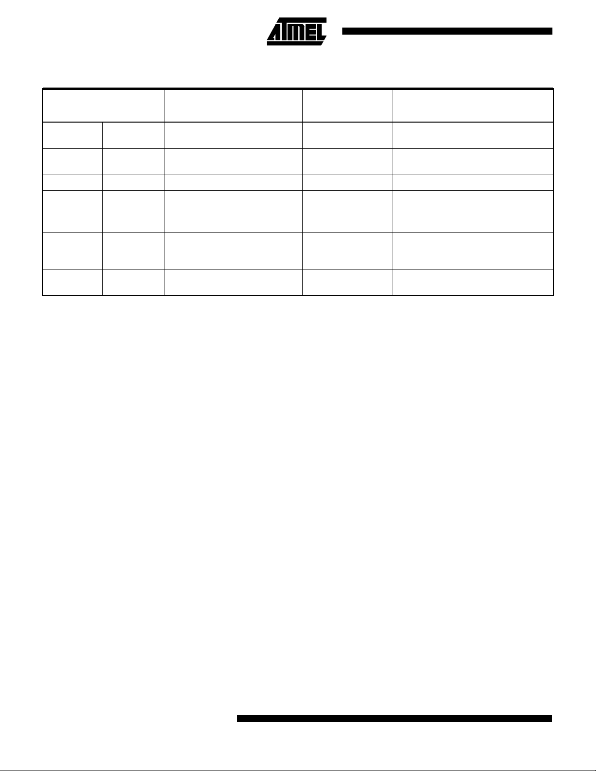
Instruction Set for the AT93C46
Address Data
Instruction SBOpCode
READ 1 10 A
EWEN 1 00 11XXXXX 11XXXX
ERASE 1 11 A
WRITE 1 01 A
ERAL 1 00 10XXXXX 10XXXX
WRAL 1 00 01XXXXX 01XXXX D
EWDS 1 00 00XXXXX 00XXXX
x 8 x 16 x 8 x 16
- A
6
0
- A
6
0
- A
6
0
A5 - A
A5 - A
A5 - A
0
0
0
D7 - D
- D
7
AT93C46/56/57/66
Comments
Reads data stored in memory, at
specified address.
Write enable must precede all
programming modes.
Erase memory location A
D
0
- D0Writes memory location A
15
Erases all memory locations. Valid
only at V
D
0
15
Writes all memory locations. Valid
- D
0
only at V
= 4.5V to 5.5V.
CC
= 4.5V to 5.5V.
CC
Disables all programming
instructions.
n - A0
n - A0
.
.
Instruction Set for the AT93C57
Address Data
Instruction SBOpCode
READ 1 10 A
EWEN 1 00 11XXXXXX 11XXXXX
ERASE 1 11 A
WRITE 1 01 A
ERAL 1 00 10XXXXXX 10XXXXX
WRAL 1 00 01XXXXXX 01XXXXX D
EWDS 1 00 00XXXXXX 00XXXXX
x 8 x 16 x 8 x 16
- A
7
0
- A
7
0
- A
7
0
A6 - A
A6 - A
A6 - A
0
0
0
D7 - D0D
- D0D
7
Comments
Reads data stored in memory, at
specified address.
Write enable must precede all
programming modes.
Erase memory location A
- D0Writes memory location A
15
Erases all memory locations. Valid
= 4.5V to 5.5V.
CC
= 4.5V to 5.5V.
CC
15
only at V
Writes all memory locations. Valid
- D
0
only at V
Disables all programming
instructions.
n - A0
n - A0
.
.
2-67
Page 6
Instruction Set for the AT9 3C5 6 and AT93C66
Address Data
Instruction SBOpCode
READ 1 10 A
EWEN 1 00 11XXXXXXX 11XXXXXX
ERASE 1 11 A
WRITE 1 01 A
ERAL 1 00 10XXXXXXX 10XXXXXX
WRAL 1 00 01XXXXXXX 01XXXXXX D
EWDS 1 00 00XXXXXXX 00XXXXXX
x 8 x 16 x 8 x 16
8
8
8
- A
- A
- A
0
0
0
A7 - A
A
7 - A0
A7 - A
0
0
D7 - D0D
- D0D
7
Comments
Reads data stored in memory, at
specified address.
Write enable must precede all
programming modes.
Erases memory location A
- D0Writes memory location A
15
Erases all memory locations. Valid
only at V
= 4.5V to 5.5V.
CC
Writes all memory locations. Valid
15
- D
0
= 5.0V ± 10% and
CC
when V
Disable Register cleared.
Disables all programming
instructions.
n - A0
n - A0
.
.
2-68 AT93C46/56/57/66
Page 7

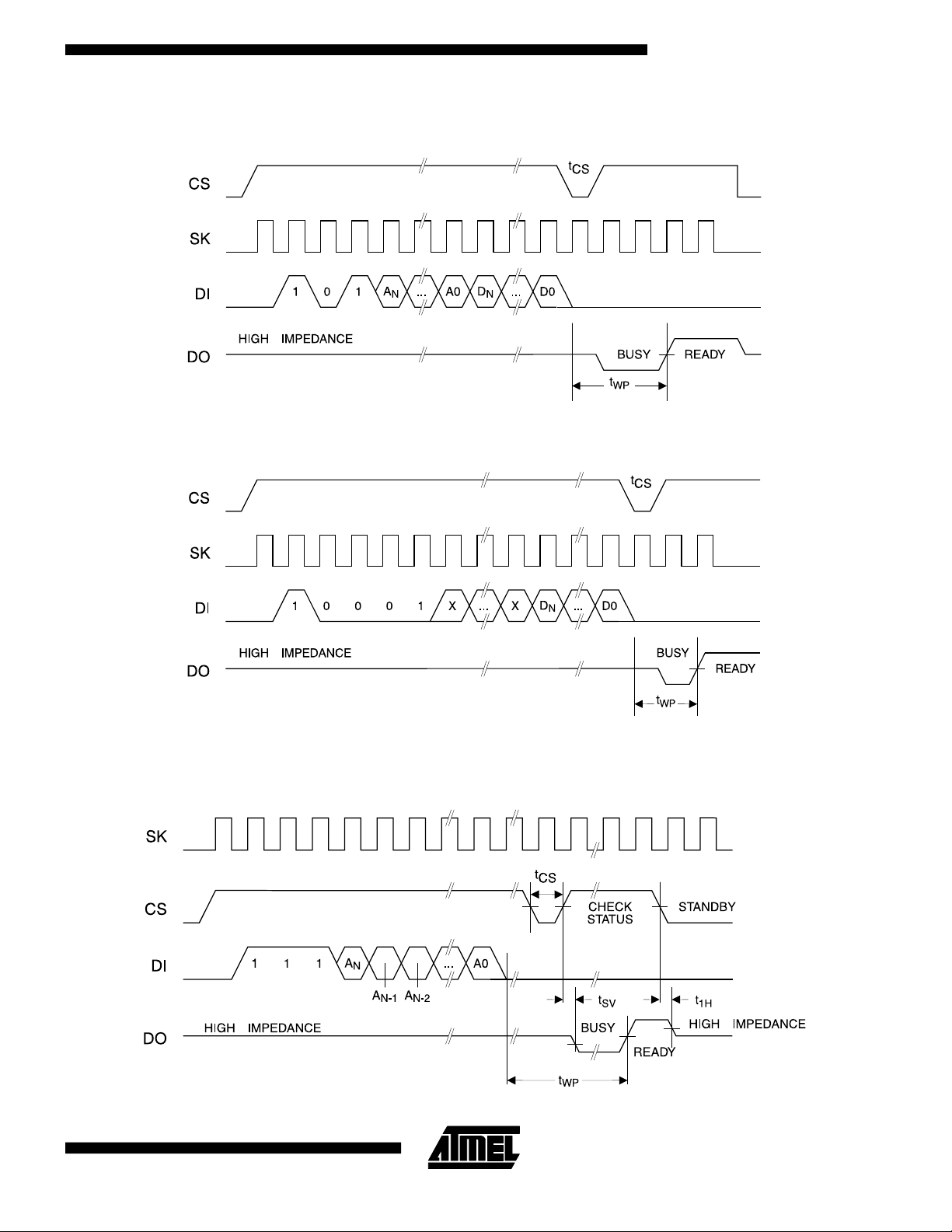
Functional Description
The AT93C46/56/57/66 is accessed via a simple and versatile 3-wire serial communication interface. Device operation is controlled by seven instructions issued by the
host processor. A valid instruction starts with a rising edge
of CS and consists of a Start Bit (logic ‘1’) followed by the
appropriate Op Code and the desired memory Address
location.
READ (READ): The Read (READ) instruction contains
the Address code for the memory location to be read. After
the instruction and address are decoded, data from the
selected memory location is available at the serial output
pin DO. Output data changes are synchronized with the
rising edges of serial clock SK. It should be noted that a
dummy bit (logic ‘0’) precedes the 8 or 16 bit data output
string.
ERASE/WRITE (EWEN): To assure data integrity, the
part automatically goes into the Erase/Write Disable
(EWDS) state when power is first applied. An Erase/Write
Enable (EWEN) instruction must be executed first before
any programming instructions can be carried out. Please
note that once in the Erase/Write Enable state, programming remains enabled until an Erase/Write Disable
(EWDS) instruction is executed or V
from the part.
ERASE (ERASE): The Erase (ERASE) instruction programs all bits in the specified memory location to the logical ‘1’ state. The self-timed erase cycle starts once the
ERASE instruction and address are decoded. The DO pin
outputs the READY/BUSY status of the part if CS is
brought high after being kept low for a minimum of 250 ns
). A logic ‘1’ at pin DO indicates that the selected mem-
(t
CS
ory location has been erased, and the part is ready for
another instruction.
power is removed
CC
AT93C46/56/57/66
WRITE (WRITE): The Write (WRITE) instruction con-
tains the 8 or 16 bits of data to be written into the specified
memory location. The self-timed programming cycle starts
after the last bit of data is received at serial data input pin
DI. The DO pin outputs the READY/BUSY status of the
part if CS is brought high after being kept low for a minimum of 250 ns (t
gramming is still in progress. A logic ‘1’ indicates that the
memory location at the specified address has been written
with the data pattern contained in the instruction and the
part is ready for further instructions. A READY/BUSY
status cannot be obtained if the CS is brought high after
the end of the self-timed programming cycle, t
ERASE ALL (ERAL): The Erase All (ERAL) instruction
programs every bit in the memory array to the logic ‘1’
state and is primarily used for testing purposes. The DO
pin outputs the READY/BUSY status of the part if CS is
brought high after being kept low for a minimum of 250 ns
). The ERAL instruction is valid only at VCC = 5.0V ±
(t
CS
10%.
WRITE ALL (WRAL): The Write All (WRAL) instruction
programs all memory locations with the data patterns
specif ied in the instr uction. The DO pin outp uts the
READY/BUSY status of the part if CS is brought high after
being kept low for a minimum of 250 ns (t
instruction is valid only at V
ERASE/WRITE DISABLE (EWDS): To protect against
accidental data disturb, the Erase/Write Disable (EWDS)
instruction disables all programming modes and should be
executed after all programming operations. The operation
of the READ instruction is independent of both the EWEN
and EWDS instructions and can be executed at any time.
). A logic ‘0’ at DO indicates that pro-
CS
.
WP
). The WRAL
CS
= 5.0V ± 10%.
CC
Timing Diagrams
Synchronous Data Timing
Note: 1. This is the minimum SK period.
(continued)
2-69
Page 8

Organization Key f or Timing Diagrams
AT93C46 (1K) AT93C56 (2K) AT93C57 (2K) AT93C66 (4K)
I/O
A
N
D
N
Note: 1. A8 is a DON’T CARE value, but the extra clock is required .
x 8 x 16 x 8 x 16 x 8 x 16 x 8 x 16
A
6
D
7
A
5
D
15
A8
D
(1)
7
A
D
Timing Diagrams (Continued)
READ Timing
15
7
A
7
D
7
A
6
D
15
A
8
D
7
A
7
D
15
EWEN Timing
EWDS Timing
(continued)
2-70 AT93C46/56/57/66
Page 9
Timing Diagrams (Continued)
WRITE Timing
AT93C46/56/57/66
WRAL Timing
Note: 1. Valid only at V
ERASE Timing
(1)
= 4.5V to 5.5V.
CC
(continued)
2-71
Page 10

Timing Diagrams (Continued)
TERAL Timing
(1)
Note: 1. Valid only at V
= 4.5V to 5.5V.
CC
2-72 AT93C46/56/57/66
Page 11

Ordering Informati o n
AT93C46/56/57/66
tWP (max)
(ms)
10 2000 30.0 2000 AT93C46-10PC 8P3 Commercial
10 800 10.0 1000 AT93C46-10PC-2.7 8P3 Commercial
10 600 10.0 500 AT93C46-10PC-2.5 8P3 Commercial
10 80 0.1 250 AT93C46-10PC-1.8 8P3 Commercial
10 2000 30.0 2000 AT93C46-10PI 8P3 Industrial
10 800 10.0 1000 AT93C46-10PI-2.7 8P3 Industrial
10 600 10.0 500 AT93C46-10PI-2.5 8P3 Industrial
10 80 0.1 250 AT93C46-10PI-1.8 8P3 Industrial
ICC (max)
(µA)
ISB (max)
(µA)
f
MAX
(kHz)
Ordering Code Package Operation Range
AT93C46-10SC 8S1 (0°C to 70°C)
AT93C46R-10SC 8S1
AT93C46W-10SC 8S2
AT93C46-10SC-2.7 8S1 (0°C to 70°C)
AT93C46R-10SC-2.7 8S1
AT93C46W-10SC-2.7 8S2
AT93C46-10SC-2.5 8S1 (0°C to 70°C)
AT93C46R-10SC-2.5 8S1
AT93C46W-10SC-2.5 8S2
AT93C46-10SC-1.8 8S1 (0°C to 70°C)
AT93C46R-10SC-1.8 8S1
AT93C46W-10SC-1.8 8S2
AT93C46-10SI 8S1 (-40°C to 85°C)
AT93C46R-10SI 8S1
AT93C46W-10SI 8S2
AT93C46-10SI-2.7 8S1 (-40°C to 85°C)
AT93C46R-10SI-2.7 8S1
AT93C46W-10SI-2.7 8S2
AT93C46-10SI-2.5 8S1 (-40°C to 85°C)
AT93C46R-10SI-2.5 8S1
AT93C46W-10SI-2.5 8S2
AT93C46-10SI-1.8 8S1 (-40°C to 85°C)
AT93C46R-10SI-1.8 8S1
AT93C46W-10SI-1.8 8S2
2-73
Page 12

Ordering Informati o n
Package Type
8P3 8 Lead, 0.30 0" Wide, Plas tic Dua l In line Packag e (PDIP)
8S1 8 Lead, 0.15 0" Wide, Plas tic Gul l Wing Small Out li ne (JEDEC SOIC)
8S2 8 Lead, 0.20 0" Wide, Plas tic Gul l Wing Small Out li ne (EIAJ SOIC)
Options
Blank Standard Device (4.5V to 5.5V)
-2.7 Low Voltage (2.7V to 5.5V)
-2.5 Low Voltage (2.5V to 5.5V)
-1.8 Low Voltage (1.8V to 5.5V)
R Rotated Pinout
2-74 AT93C46/56/57/66
Page 13

Ordering Informati o n
AT93C46/56/57/66
tWP (max)
(ms)
10 2000 30.0 2000 AT93C56-10PC 8P3 Commercial
10 800 10.0 1000 AT93C56-10PC-2.7 8P3 Commercial
10 600 10.0 500 AT93C56-10PC-2.5 8P3 Commercial
10 80 0.1 250 AT93C56-10PC-1.8 8P3 Commercial
10 2000 30.0 2000 AT93C56-10PI 8P3 Industrial
10 800 10.0 1000 AT93C56-10PI-2.7 8P3 Industrial
10 600 10.0 500 AT93C56-10PI-2.5 8P3 Industrial
10 80 0.1 250 AT93C56-10PI-1.8 8P3 Industrial
ICC (max)
(µA)
ISB (max)
(µA)
f
MAX
(kHz)
Ordering Code Package Operation Range
AT93C56-10SC 8S1 (0°C to 70°C)
AT93C56W-10SC 8S2
AT93C56-10SC-2.7 8S1 (0°C to 70°C)
AT93C56W-10SC-2.7 8S2
AT93C56-10SC-2.5 8S1 (0°C to 70°C)
AT93C56W-10SC-2.5 8S2
AT93C56-10SC-1.8 8S1 (0°C to 70°C)
AT93C56W-10SC-1.8 8S2
AT93C56-10SI 8S1 (-40°C to 85°C)
AT93C56W-10SI 8S2
AT93C56-10SI-2.7 8S1 (-40°C to 85°C)
AT93C56W-10SI-2.7 8S2
AT93C56-10SI-2.5 8S1 (-40°C to 85°C)
AT93C56W-10SI-2.5 8S2
AT93C56-10SI-1.8 8S1 (-40°C to 85°C)
AT93C56W-10SI-1.8 8S2
Package Type
8P3 8 Lead, 0.30 0" Wide, Plas tic Dua l In line Packag e (PDIP)
8S1 8 Lead, 0.15 0" Wide, Plas tic Gul l Wing Small Out li ne (JEDEC SOIC)
8S2 8 Lead, 0.20 0" Wide, Plas tic Gul l Wing Small Out li ne (EIAJ SOIC)
Options
Blank Standard Device (4.5V to 5.5V)
-2.7 Low Voltage (2.7V to 5.5V)
-2.5 Low Voltage (2.5V to 5.5V)
-1.8 Low Voltage (1.8V to 5.5V)
2-75
Page 14

Ordering Informati o n
tWP (max)
(ms)
ICC (max)
(µA)
ISB (max)
(µA)
f
MAX
(kHz)
Ordering Code Package Operation Range
10 2000 30.0 2000 AT93C57-10PC 8P3 Commercial
AT93C57-10SC 8S1 (0°C to 70°C)
AT93C57W-10SC 8S2
10 800 10.0 1000 AT93C57-10PC-2.7 8P3 Commercial
AT93C57-10SC-2.7 8S1 (0°C to 70°C)
AT93C57W-10SC-2.7 8S2
10 600 10.0 500 AT93C57-10PC-2.5 8P3 Commercial
AT93C57-10SC-2.5 8S1 (0°C to 70°C)
AT93C57W-10SC-2.5 8S2
10 80 0.1 250 AT93C57-10PC-1.8 8P3 Commercial
AT93C57-10SC-1.8 8S1 (0°C to 70°C)
AT93C57W-10SC-1.8 8S2
10 2000 30.0 2000 AT93C57-10PI 8P3 Industrial
AT93C57-10SI 8S1 (-40°C to 85°C)
AT93C57W-10SI 8S2
10 800 10.0 1000 AT93C57-10PI-2.7 8P3 Industrial
AT93C57-10SI-2.7 8S1 (-40°C to 85°C)
AT93C57W-10SI-2.7 8S2
10 600 10.0 500 AT93C57-10PI-2.5 8P3 Industrial
AT93C57-10SI-2.5 8S1 (-40°C to 85°C)
AT93C57W-10SI-2.5 8S2
10 80 0.1 250 AT93C57-10PI-1.8 8P3 Industrial
AT93C57-10SI-1.8 8S1 (-40°C to 85°C)
AT93C57W-10SI-1.8 8S2
Package Type
8P3 8 Lead, 0.30 0" Wide, Plas tic Dua l In line Packag e (PDIP)
8S1 8 Lead, 0.15 0" Wide, Plas tic Gul l Wing Small Out li ne (JEDEC SOIC)
8S2 8 Lead, 0.20 0" Wide, Plas tic Gul l Wing Small Out li ne (EIAJ SOIC)
Options
Blank Standard Device (4.5V to 5.5V)
-2.7 Low Voltage (2.7V to 5.5V)
-2.5 Low Voltage (2.5V to 5.5V)
-1.8 Low Voltage (1.8V to 5.5V)
2-76 AT93C46/56/57/66
Page 15

Ordering Informati o n
AT93C46/56/57/66
tWP (max)
(ms)
10 2000 30.0 2000 AT93C66-10PC 8P3 Commercial
10 800 10.0 1000 AT93C66-10PC-2.7 8P3 Commercial
10 600 10.0 500 AT93C66-10PC-2.5 8P3 Commercial
10 80 0.1 250 AT93C66-10PC-1.8 8P3 Commercial
10 2000 30.0 2000 AT93C66-10PI 8P3 Industrial
10 800 10.0 1000 AT93C66-10PI-2.7 8P3 Industrial
10 600 10.0 500 AT93C66-10PI-2.5 8P3 Industrial
10 80 0.1 250 AT93C66-10PI-1.8 8P3 Industrial
ICC (max)
(µA)
ISB (max)
(µA)
f
MAX
(kHz)
Ordering Code Package Operation Range
AT93C66-10SC 8S1 (0°C to 70°C)
AT93C66W-10SC 8S2
AT93C66-10SC-2.7 8S1 (0°C to 70°C)
AT93C66W-10SC-2.7 8S2
AT93C66-10SC-2.5 8S1 (0°C to 70°C)
AT93C66W-10SC-2.5 8S2
AT93C66-10SC-1.8 8S1 (0°C to 70°C)
AT93C66W-10SC-1.8 8S2
AT93C66-10SI 8S1 (-40°C to 85°C)
AT93C66W-10SI 8S2
AT93C66-10SI-2.7 8S1 (-40°C to 85°C)
AT93C66W-10SI-2.7 8S2
AT93C66-10SI-2.5 8S1 (-40°C to 85°C)
AT93C66W-10SI-2.5 8S2
AT93C66-10SI-1.8 8S1 (-40°C to 85°C)
AT93C66W-10SI-1.8 8S2
Package Type
8P3 8 Lead, 0.30 0" Wide, Plas tic Dua l In line Packag e (PDIP)
8S1 8 Lead, 0.15 0" Wide, Plas tic Gul l Wing Small Out li ne (JEDEC SOIC)
8S2 8 Lead, 0.20 0" Wide, Plas tic Gul l Wing Small Out li ne (EIAJ SOIC)
Options
Blank Standard Device (4.5V to 5.5V)
-2.7 Low Voltage (2.7V to 5.5V)
-2.5 Low Voltage (2.5V to 5.5V)
-1.8 Low Voltage (1.8V to 5.5V)
2-77
 Loading...