

Features
1
2
3
4
8
7
6
5
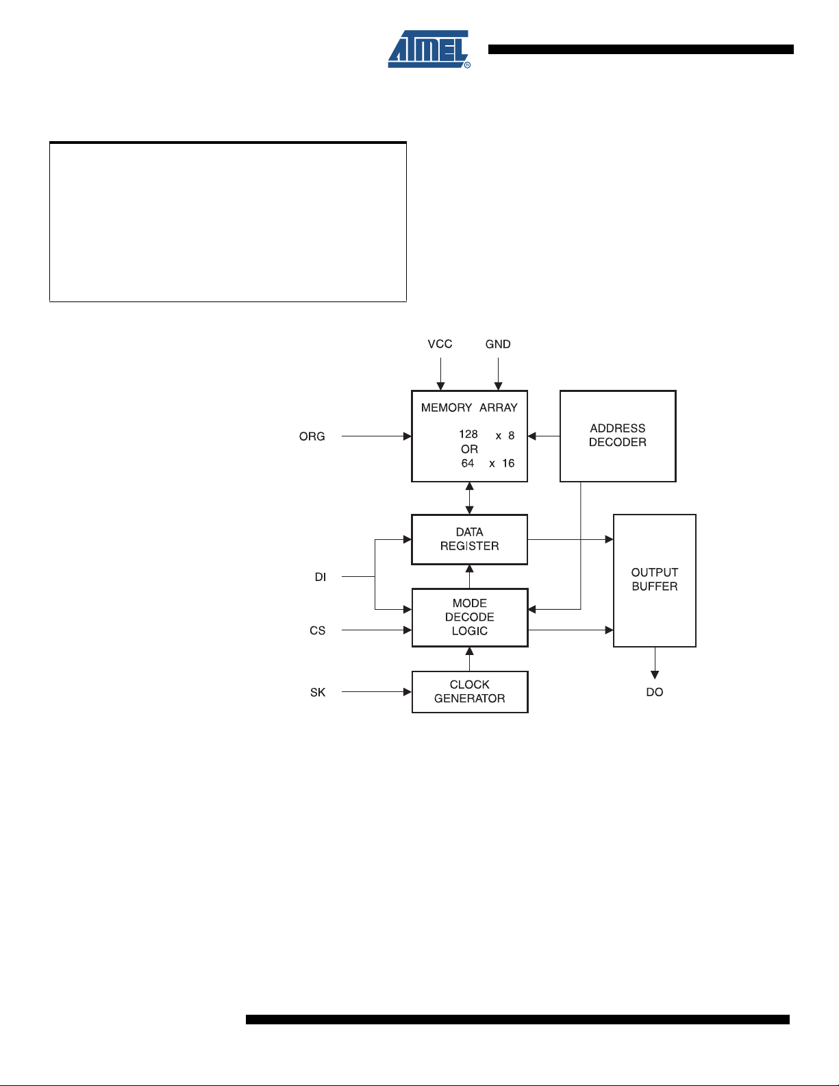
CS
SK
DI
DO
VCC
NC
ORG
GND
VCC
NC
ORG
GND
CS
SK
D1
D0
1
2
3
4
8
7
6
5
1
2
3
4
8
7
6
5
CS
SK
DI
DO
VCC
NC
ORG
GND
1
2
3
4
8
7
6
5
VCC
NC
ORG
GND
CS
SK
DI
DO
1
2
3
4
8
7
6
5
CS
SK
DI
DO
VCC
NC
ORG
GND
8-lead SOIC
8-lead dBGA2
8-lead PDIP
8-lead Ultra Thin mini-MAP (MLP 2x3)
8-lead TSSOP
Bottom View
Bottom View
• Low-voltage and Standard-voltage Operation
– 1.8 (V
= 1.8V to 5.5V)
CC
• User-selectable Internal Organization
– 1K: 128 x 8 or 64 x 16
• Three-wire Serial Interface
• 2 MHz Clock Rate (5V)
• Self-timed Write Cycle (5 ms max)
• High Reliability
– Endurance: 1 Million Write Cycles
– Data Retention: 100 Years
• 8-lead JEDEC PDIP, 8-lead JEDEC SOIC, 8-lead Ultra Thin mini-MAP (MLP 2x3), 8-lead
TSSOP and 8-ball dBGA2 Packages
• Die Sales: Wafer Form, Tape and Reel, and Bumped Wafers
Description
The AT93C46D provides 1024 bits of serial electrically erasable programmable readonly memory (EEPROM), organized as 64 words of 16 bits each (when the ORG pin is
connected to VCC), and 128 words of 8 bits each (when the ORG pin is tied to
ground). The device is optimized for use in many industrial and commercial applications where low-power and low-voltage operations are essential. The AT93C46D is
available in space-saving 8-lead PDIP, 8-lead JEDEC SOIC, 8-lead Ultra Thin miniMAP (MLP 2x3), 8-lead TSSOP, and 8-lead dBGA2 packages.
Three-wire
Serial
EEPROM
1K (128 x 8 or 64 x 16)
AT93C46D
The AT93C46D is enabled through the Chip Select pin (CS) and accessed via a
three-wire serial interface consisting of Data Input (DI), Data Output (DO), and Shift
Clock (SK). Upon receiving a Read instruction at DI, the address is decoded and the
data is clocked out serially on the DO pin. The Write cycle is completely self-timed,
and no separate Erase cycle is required before Write. The Write cycle is only enabled
when the part is in the Erase/Write Enable state. When CS is brought high following
the initiation of a Write cycle, the DO pin outputs the Ready/Busy status of the part.
The AT93C46D is available in 1.8 (1.8V to 5.5V) version.
Table 0-1. Pin Configurations
Pin Name Function
CS Chip Select
SK Serial Data Clock
DI Serial Data Input
DO Serial Data Output
GND Ground
VCC Power Supply
ORG Internal Organization
NC No Connect
5193F–SEEPR–1/08
1. Absolute Maximum Ratings*
Operating Temperature ......................................−55°C to +125°C
Storage Temperature .........................................−65°C to +150°C
Voltage on Any Pin
with Respect to Ground ........................................ −1.0V to +7.0V
Maximum Operating Voltage .......................................... 6.25V
DC Output Current........................................................ 5.0 mA
Figure 1-1. Block Diagram
*NOTICE: Stresses beyond those listed under “Absolute
Maximum Ratings” may cause permanent damage to the device. This is a stress rating only, and
functional operation of the device at these or any
other conditions beyond those indicated in the
operational sections of this specification is not
implied. Exposure to absolute maximum rating
conditions for extended periods may affect
device reliability
Notes: 1. When the ORG pin is connected to VCC, the “x 16” organization is selected. When it is con-
nected to ground, the “x 8” organization is selected. If the ORG pin is left unconnected and the
application does not load the input beyond the capability of the internal 1 Meg ohm pullup, then
the “x 16” organization is selected.
2. For the AT93C46D, if the “x 16” organization is the mode of choice and pin 6 (ORG) is left
unconnected, Atmel
AT93C46E datasheet.
2
AT93C46D
®
recommends using AT93C46E device. For more details, see the
5193F–SEEPR–1/08
AT93C46D
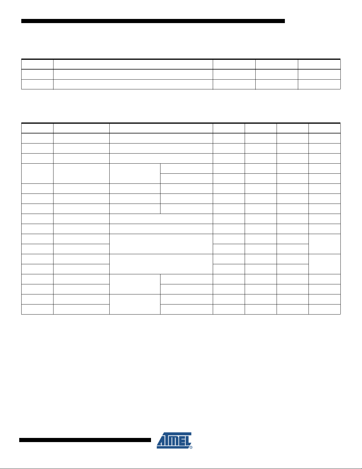
Table 1-1. Pin Capacitance
(1)
Applicable over recommended operating range from TA = 25°C, f = 1.0 MHz, VCC = +1.8V (unless otherwise noted)
Symbol Test Conditions Max Units Conditions
C
OUT
C
IN
Output Capacitance (DO) 5 pF V
OUT
= 0V
Input Capacitance (CS, SK, DI) 5 pF VIN = 0V
Note: 1. This parameter is characterized and is not 100% tested.
Table 1-2. DC Characteristics
Applicable over recommended operating range from: T
Symbol Parameter Test Condition Min Typ Max Unit
V
CC1
V
CC2
V
CC3
I
CC
I
SB1
I
SB2
I
SB3
I
IL
I
OL
(1)
V
IL1
(1)
V
IH1
(1)
V
IL2
(1)
V
IH2
V
OL1
V
OH1
V
OL2
V
OH2
Note: 1. VIL min and VIH max are reference only and are not tested.
Supply Voltage 1.8 5.5 V
Supply Voltage 2.7 5.5 V
Supply Voltage 4.5 5.5 V
Supply Current VCC = 5.0V
Standby Current VCC = 1.8V CS = 0V 0.4 1.0 µA
Standby Current VCC = 2.7V CS = 0V 6.0 10.0 µA
Standby Current VCC = 5.0V CS = 0V 10.0 15.0 µA
Input Leakage VIN = 0V to VCC 0.1 1.0 µA
Output Leakage VIN = 0V to VCC 0.1 1.0 µA
Input Low Voltage
2.7V ≤ V
Input High Voltage 2.0 VCC + 1
Input Low Voltage
1.8V ≤ V
Input High Voltage VCC x 0.7 VCC + 1
Output Low Voltage
2.7V ≤ VCC ≤ 5.5V
Output High Voltage IOH = −0.4 mA 2.4 V
Output Low Voltage
Output High Voltage IOH = −100 µA VCC – 0.2 V
1.8V ≤ V
≤ 2.7V
CC
= −40°C to +85°C, VCC = +1.8V to +5.5V (unless otherwise noted)
AI
READ at 1.0 MHz 0.5 2.0 mA
WRITE at 1.0 MHz 0.5 2.0 mA
−0.6 0.8
≤ 5.5V
CC
≤ 2.7V
−0.6 V
CC
IOL = 2.1 mA 0.4 V
I
= 0.15 mA 0.2 V
OL
CC
x 0.3
V
V
5193F–SEEPR–1/08
3

Table 1-3. AC Characteristics
Applicable over recommended operating range from T
= −40°C to + 85°C, VCC = +2.7V to +5.5V,
AI
CL = 1 TTL Gate and 100 pF (unless otherwise noted)
Symbol Parameter Test Condition Min Typ Max Units
f
SK
t
SKH
t
SKL
t
CS
t
CSS
t
DIS
t
CSH
t
DIH
t
PD1
t
PD0
t
SV
t
DF
t
WP
Endurance
(1)
SK Clock
Frequency
4.5V ≤ V
2.7V ≤ V
1.8V ≤ V
4.5V ≤ V
SK High Time
2.7V ≤ V
1.8V ≤ V
4.5V ≤ V
SK Low Time
2.7V ≤ V
1.8V ≤ V
Minimum CS
Low Time
4.5V ≤ V
2.7V ≤ V
1.8V ≤ V
CS Setup Time Relative to SK
DI Setup Time Relative to SK
CS Hold Time Relative to SK 0 ns
DI Hold Time Relative to SK
Output Delay to “1” AC Test
Output Delay to “0” AC Test
CS to Status Valid AC Test
CS to DO in High
Impedance
AC Test
CS = V
Write Cycle Time
5.0V, 25°C 1M Write Cycles
CC
CC
CC
CC
CC
CC
CC
CC
CC
CC
CC
CC
IL
≤ 5.5V
≤ 5.5V
≤ 5.5V
≤ 5.5V
≤ 5.5V
≤ 5.5V
≤ 5.5V
≤ 5.5V
≤ 5.5V
≤ 5.5V
≤ 5.5V
≤ 5.5V
Note: 1. This parameter is ensured by characterization.
4.5V ≤ V
2.7V ≤ V
1.8V ≤ V
4.5V ≤ V
2.7V ≤ V
1.8V ≤ V
4.5V ≤ V
2.7V ≤ V
1.8V ≤ V
4.5V ≤ V
2.7V ≤ V
1.8V ≤ V
4.5V ≤ V
2.7V ≤ V
1.8V ≤ V
4.5V ≤ V
2.7V ≤ V
1.8V ≤ V
≤ 5.5V
CC
≤ 5.5V
CC
≤ 5.5V
CC
≤ 5.5V
CC
≤ 5.5V
CC
≤ 5.5V
CC
≤ 5.5V
CC
≤ 5.5V
CC
≤ 5.5V
CC
≤ 5.5V
CC
≤ 5.5V
CC
≤ 5.5V
CC
≤ 5.5V
CC
≤ 5.5V
CC
≤ 5.5V
CC
≤ 5.5V
CC
≤ 5.5V
CC
≤ 5.5V
CC
4.5V ≤ VCC ≤ 5.5V
2.7V ≤ V
1.8V ≤ V
1.8V ≤ V
≤ 5.5V
CC
≤ 5.5V
CC
≤ 5.5V 0.1 3 5 ms
CC
0
0
0
250
250
1000
250
250
1000
250
250
1000
50
50
200
100
100
400
100
100
400
2
1
0.25
250
250
1000
250
250
1000
250
250
1000
100
150
400
MHz
ns
ns
ns
ns
ns
ns
ns
ns
ns
ns
4
AT93C46D
5193F–SEEPR–1/08
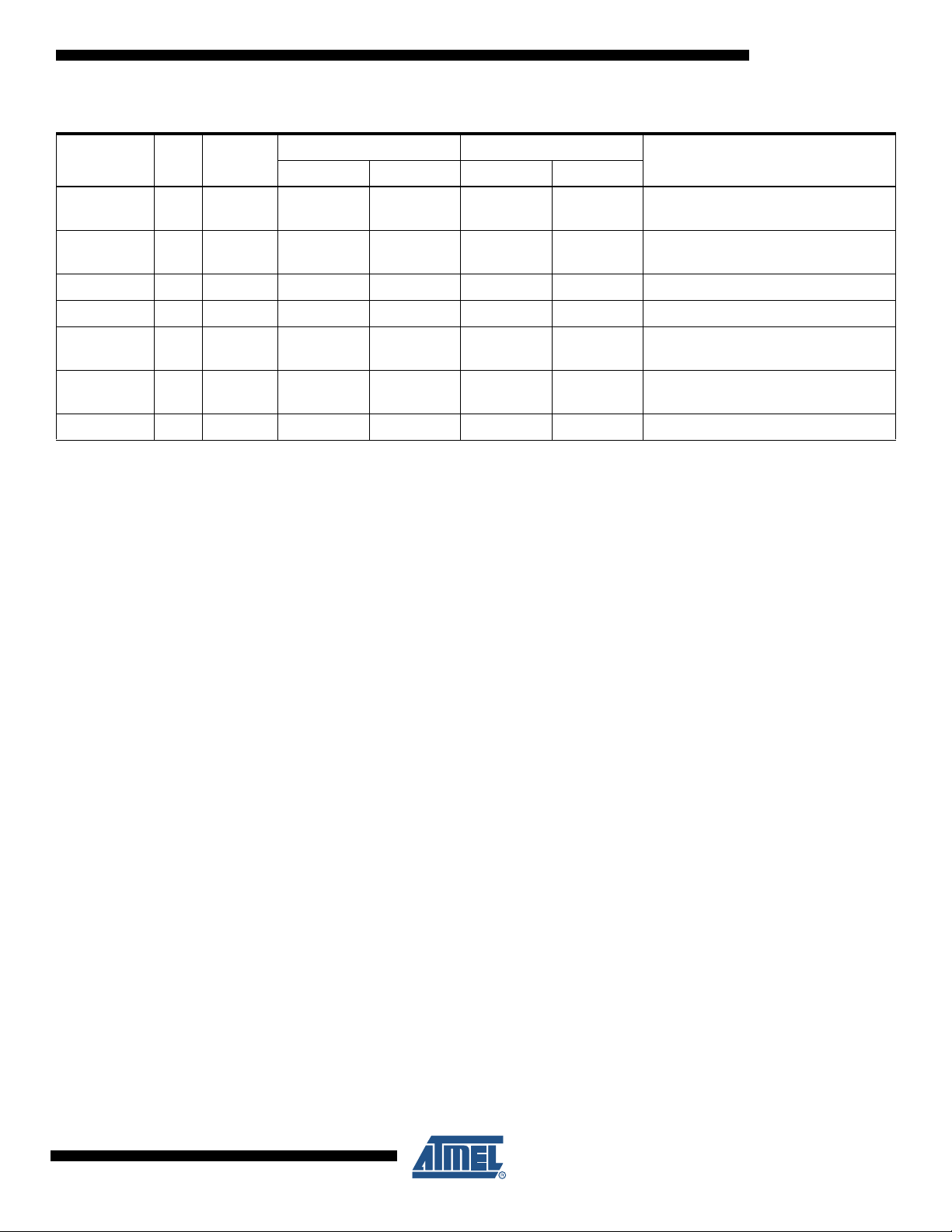
Table 1-4. Instruction Set for the AT93C46D
AT93C46D
Op
Instruction SB
Code
READ 1 10 A6 – A
EWEN 1 00 11XXXXX 11XXXX
ERASE 1 11 A6 – A
WRITE 1 01 A6 – A
ERAL 1 00 10XXXXX 10XXXX
WRAL 1 00 01XXXXX 01XXXX D7 – D
Address Data
0
0
0
A5 – A
A5 – A
A5 – A
0
0
0
D7 – D
0
0
Commentsx 8 x 16 x 8 x 16
Reads data stored in memory, at
specified address
Write enable must precede all
programming modes
Erases memory location An – A
D
15
– D
Writes memory location An – A
0
0
0
Erases all memory locations. Valid
only at V
D
– D
15
Writes all memory locations. Valid
0
only at VCC = 4.5V to 5.5V
= 4.5V to 5.5V
CC
EWDS 1 00 00XXXXX 00XXXX Disables all programming instructions
Note: The Xs in the address field represent DON’T CARE values and must be clocked.
2. Functional Description
The AT93C46D is accessed via a simple and versatile three-wire serial communication interface. Device operation is controlled by seven instructions issued by the host processor. A valid
instruction starts with a rising edge of CS and consists of a start bit (logic “1”) followed by the
appropriate op code and the desired memory address location.
READ (READ): The Read (READ) instruction contains the address code for the memory location to be read. After the instruction and address are decoded, data from the selected memory
location is available at the serial output pin DO. Output data changes are synchronized with the
rising edges of serial clock SK. It should be noted that a dummy bit (logic “0”) precedes the 8- or
16-bit data output string.
ERASE/WRITE ENABLE (EWEN): To assure data integrity, the part automatically goes into the
Erase/Write Disable (EWDS) state when power is first applied. An Erase/Write Enable (EWEN)
instruction must be executed first before any programming instructions can be carried out.
Please note that once in the EWEN state, programming remains enabled until an EWDS instruction is executed or V
power is removed from the part.
CC
ERASE (ERASE): The Erase (ERASE) instruction programs all bits in the specified memory
location to the logical “1” state. The self-timed erase cycle starts once the Erase instruction and
address are decoded. The DO pin outputs the Ready/Busy status of the part if CS is brought
high after being kept low for a minimum of 250 ns (t
). A logic “1” at pin DO indicates that the
CS
selected memory location has been erased and the part is ready for another instruction.
WRITE (WRITE): The Write (WRITE) instruction contains the 8 or 16 bits of data to be written
into the specified memory location. The self-timed programming cycle t
starts after the last bit
WP
of data is received at serial data input pin DI. The DO pin outputs the Read/Busy status of the
part if CS is brought high after being kept low for a minimum of 250 ns (t
). A logic “0” at DO
CS
indicates that programming is still in progress. A logic “1” indicates that the memory location at
the specified address has been written with the data pattern contained in the instruction and the
5193F–SEEPR–1/08
5

part is ready for further instructions. A Ready/Busy status cannot be obtained if the CS is
brought high after the end of the self-timed programming cycle tWP.
ERASE ALL (ERAL): The Erase All (ERAL) instruction programs every bit in the memory array
to the logic “1” state and is primarily used for testing purposes. The DO pin outputs the
Ready/Busy status of the part if CS is brought high after being kept low for a minimum of 250 ns
(t
). The ERAL instruction is valid only at VCC = 5.0V ± 10%.
CS
WRITE ALL (WRAL): The Write All (WRAL) instruction programs all memory locations with the
data patterns specified in the instruction. The DO pin outputs the Ready/Busy status of the part if
CS is brought high after being kept low for a minimum of 250 ns (t
valid only at V
= 5.0V ± 10%.
CC
). The WRAL instruction is
CS
ERASE/WRITE DISABLE (EWDS): To protect against accidental data disturb, the Erase/Write
Disable (EWDS) instruction disables all programming modes and should be executed after all
programming operations. The operation of the Read instruction is independent of both the
EWEN and EWDS instructions and can be executed at any time.
6
AT93C46D
5193F–SEEPR–1/08
3. Timing Diagrams
μs
High Impedance
t
CS
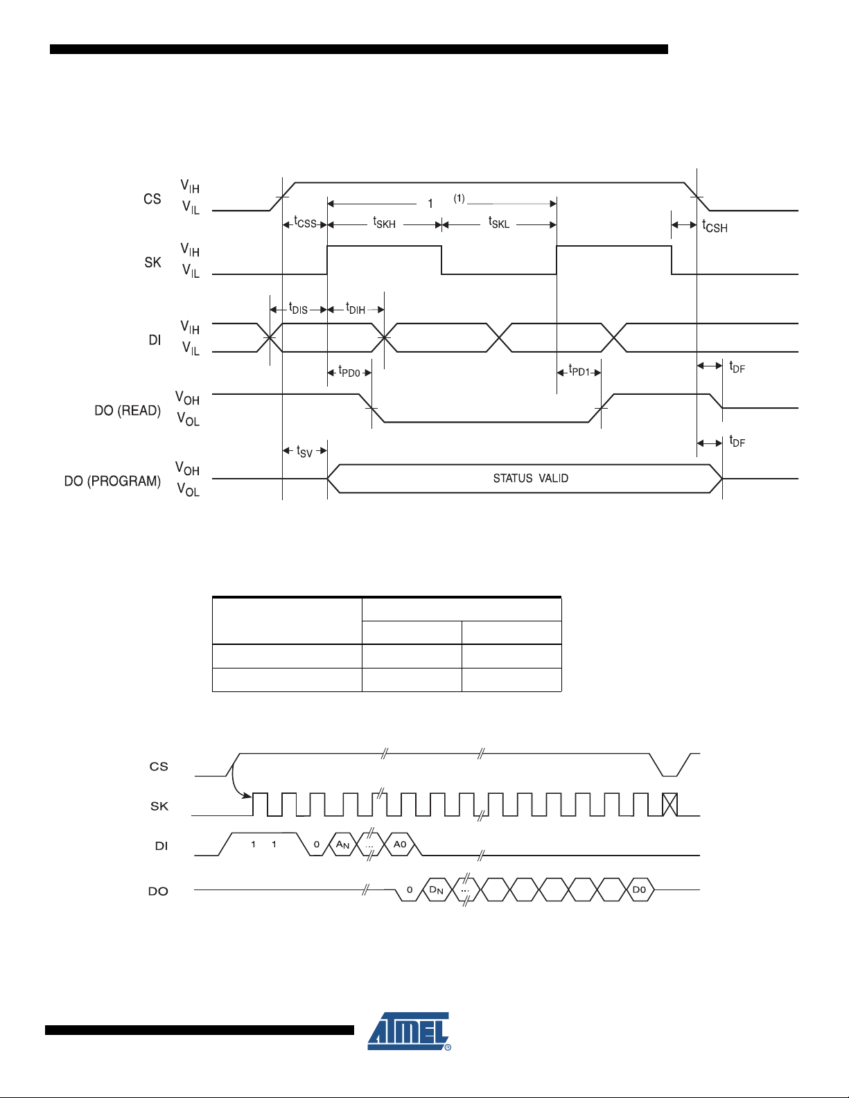
Figure 3-1. Synchronous Data Timing
AT93C46D
Note: 1. This is the minimum SK period.
Table 3-1. Organization Key for Timing Diagrams
I/O
A
D
Figure 3-2. READ Timing
AT93C46D (1K)
x 8 x 16
N
N
A
6
D
7
A
5
D
15
5193F–SEEPR–1/08
7
 Loading...