

ATMEL AT93C46C-10SI-2.7, AT93C46C-10SI-2.5, AT93C46C-10SI, AT93C46C-10SC-2.7, AT93C46C-10SC-2.5 Datasheet
...
Features
•
Low-Voltage and Standard-Voltage Operation
– 5.0 (VCC = 4.5V to 5.5V)
– 2.7 (VCC = 2.7V to 5.5V)
– 2.5 (VCC = 2.5V to 5.5V)
•
3-Wire Serial Interface
•
Schmitt Trigger, Filtered Inputs for Noise Suppression
•
2 MHz Clock Rate (5V) Compatibility
•
Self-Timed Write Cycle (10 ms max)
•
High Reliability
– Endurance: 1 Million Write Cycles
– Data Retention: 100 Years
– ESD Protection: > 4000V
•
Automotive Grade and Extended Temperature Devices Available
•
8-Pin PDIP and JEDEC SOIC Packages
Description
The AT93C46C provides 1024 bits of serial electrically-erasable programmable read
only memory (EEPROM) organized as 64 words of 16 bits each. The devi ce is optimized for use in many industrial and commercial appl ications where lo w-power and
low-voltage operation are essential. The AT93C46C is available in space saving 8-pin
PDIP and 8-pin JEDEC packages.
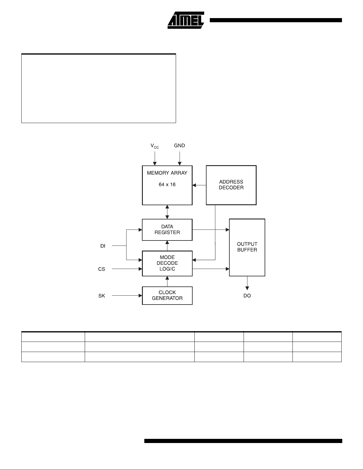
The AT93C46C is enabled through the Chip Select pin (CS) , and accessed vi a a 3wire serial interface consisting of Data Input (DI), Data Output (DO), and Shift Clock
(SK). Upon receiving a READ instruction at DI, the address is decoded and the data is
clocked out serially on the data output pin DO. The WRITE cycl e is completely selftimed and no separate ERASE cycle is required before WRITE. The WRITE cycle is
only enabled when the part is in the ERASE/WRITE ENABLE state. When CS is
brought “high” followin g the initiation of a WRITE cy cle, the DO pin outputs the
READY/BUSY status of the part.
The AT93C46C is available in 4.5V to 5.5V, 2.7V to 5.5V, and 2.5V to 5.5V versions.
3-Wire
Serial EEPROM
1K (64 x 16)
AT93C46C
Pin Configurations
Pin Name Function
CS Chip Select
SK Serial Data Clock
DI Serial Data Input
DO Serial Data Output
GND Ground
VCC Power Supply
NC No Connect
DC Don’t Connect
CS
SK
DI
DO
CS
SK
DI
DO
8-Pin PDIP
1
2
3
4
8-Pin SOIC
1
2
3
4
8
VCC
7
DC
6
NC
5
GND
VCC
8
DC
7
NC
6
GND
5
3-Wire, 1K
Serial E
2
PROM
Rev. 1122A–07/98
1
Absolute Maximum Ratings*
Operating Temperature.................................. -55°C to +125°C
Storage Temperature..................................... -65°C to +150°C
Voltage on Any Pin
with Respect to Ground.....................................-1.0V to +7.0V
Maximum Operating Voltage........................................... 6.25V
DC Output Current........................................................5.0 mA
Block Diagram
*NOTICE: Stresses beyond those listed under “Absolute
Maximum Ratings” may cause permanent damage to the de vic e. T his is a stres s r ating o nly an d
functional opera tion of the device at these or any
other conditions beyond those indicated in the
operational sections of this specification is not
implied. Exposure to absolute maximum rating
conditions for extended periods may affect
device reli abi li ty.
Pin Capacitance
(1)
Applicable over recommended operating range from TA = 25°C, f = 1.0 MHz, VCC = +5.0V (unless otherwise noted).
Test Conditions Max Units Conditions
C
OUT
C
IN
Note: 1. This parameter is characterized and is not 100% tested.
2
Output Capacitance (DO) 5 pF V
Input Capacitance (CS, SK, DI) 5 pF VIN = 0V
OUT
= 0V
AT93C46C
AT93C46C
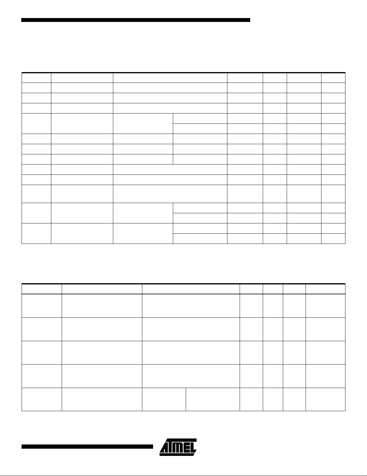
DC Characteristics
Applicable over recommended operating range from: TAI = -40°C to +85°C, VCC = +2.5V to +5.5V,
= 0°C to +70°C, VCC = +2.5V to +5.5V (unless otherwise noted).
T
AC
Symbol Parameter Test Condition Min Typ Max Units
V
V
V
I
I
I
I
I
I
V
V
V
V
V
V
CC1
CC2
CC3
CC
SB1
SB2
SB3
IL
OL
IL1
IH1
OL1
OH1
OL2
OH2
(1)
(1)
Supply Voltage 2.5 5.5 V
Supply Voltage 2.7 5.5 V
Supply Voltage 4.5 5.5 V
Supply Current
V
= 5.0V
CC
READ at 1.0 MHz 0.5 2.0 mA
WRITE at 1.0 MHz 0.5 2.0 mA
Standby Current VCC = 2.5V CS = 0V 14.0 20.0 µA
Standby Current VCC = 2.7V CS = 0V 14.0 20.0 µA
Standby Current VCC = 5.0V CS = 0V 35.0 50.0 µA
Input Leakage VIN = 0V to VCC 0.1 1.0 µA
Output Leakage VIN = 0V to VCC 0.1 1.0 µA
Input Low Voltage
Input High Voltage
Output Low Voltage
Output High Voltage
Output Low Voltage
Output High Voltage
2.5V ≤ VCC ≤ 5.5V
4.5V ≤ V
2.5V ≤ V
≤ 5.5V
CC
≤ 2.7V
CC
I
= 2.1 mA 0.4 V
OL
I
= -0.4 mA 2.4 V
OH
= 0.15 mA 0.2 V
I
OL
IOH = -100 µAV
Note: 1. VIL min and VIH max are reference only and are not tested.
-0.6
V
x 0.7
CC
- 0.2 V
CC
x 0.3
V
CC
V
+ 1
CC
V
AC Characteristics
Applicable over recommended operating range from TA = -40°C to + 85°C, VCC = +2.5V to + 5.5V,
CL = 1 TTL Gate and 100 pF (unless otherwise noted).
Symbol Parameter Test Condition Min Typ Max Units
f
t
t
t
t
SK
SKH
SKL
CS
CSS
SK Clock Frequency 4.5V ≤ VCC ≤ 5.5V
2.7V ≤ V
2.5V ≤ V
≤ 5.5V
CC
≤ 5.5V
CC
SK High Time 4.5V ≤ VCC ≤ 5.5V
2.7V ≤ V
2.5V ≤ V
≤ 5.5V
CC
≤ 5.5V
CC
SK Low Time 4.5V ≤ VCC ≤ 5.5V
2.7V ≤ V
2.5V ≤ V
≤ 5.5V
CC
≤ 5.5V
CC
Minimum CS Low Time 4.5V ≤ VCC ≤ 5.5V
2.7V ≤ V
2.5V ≤ V
≤ 5.5V
CC
≤ 5.5V
CC
CS Setup Time Relative to SK 4.5V ≤ VCC ≤ 5.5V
2.7V ≤ V
2.5V ≤ V
≤ 5.5V
CC
≤ 5.5V
CC
0
0
0
250
250
500
250
250
500
250
250
500
50
50
100
2
1
0.5
MHz
ns
ns
ns
ns
3
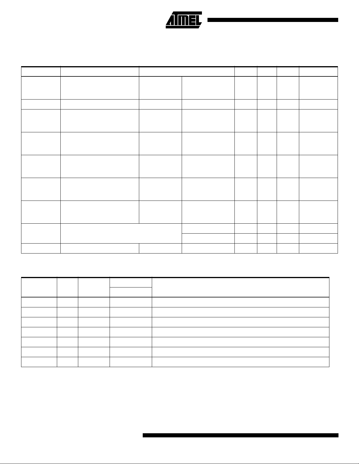
AC Characteristics (Continued)
Applicable over recommended operating range from TA = -40°C to + 85°C, VCC = +2.5V to + 5.5V,
CL = 1 TTL Gate and 100 pF (unless otherwise noted).
Symbol Parameter Test Condition Min Typ Max Units
t
DIS
t
CSH
t
DIH
t
PD1
t
PD0
t
SV
t
DF
t
WP
Endurance
Note: 1. This parameter is characterized and is not 100% tested.
DI Setup Time Relative to SK 4.5V ≤ VCC ≤ 5.5V
2.7V ≤ V
2.5V ≤ V
≤ 5.5V
CC
≤ 5.5V
CC
100
100
200
CS Hold Time Relative to SK 0 ns
DI Hold Time Relative to SK 4.5V ≤ VCC ≤ 5.5V
2.7V ≤ V
2.5V ≤ V
≤ 5.5V
CC
≤ 5.5V
CC
Output Delay to ‘1’ AC Test 4.5V ≤ VCC ≤ 5.5V
2.7V ≤ V
2.5V ≤ V
≤ 5.5V
CC
≤ 5.5V
CC
Output Delay to ‘0’ AC Test 4.5V ≤ VCC ≤ 5.5V
2.7V ≤ V
2.5V ≤ V
≤ 5.5V
CC
≤ 5.5V
CC
CS to Status Valid AC Test 4.5V ≤ VCC ≤ 5.5V
≤ 5.5V
CC
≤ 5.5V
CC
≤ 5.5V
CC
≤ 5.5V
CC
CS to DO in High Impedance AC Test
CS = V
2.7V ≤ V
2.5V ≤ V
4.5V ≤ VCC ≤ 5.5V
IL
2.7V ≤ V
2.5V ≤ V
100
100
200
250
250
500
250
250
500
250
250
500
100
100
200
Write Cycle Time 0.1 10 ms
4.5V ≤ V
(1)
5.0V, 25°C, Page Mode 1 M Write Cycle
≤ 5.5V 1 ms
CC
ns
ns
ns
ns
ns
ns
Instruction Set for the AT93C46C
Address
Instruction SB Op Code
READ 1 10 A
5
- A
0
EWEN 1 00 11XXXX Write enable must precede all programming modes.
ERASE 1 11 A
WRITE 1 01 A
5
5
- A
- A
0
0
ERAL 1 00 10XXXX Erases all memory locations. Valid only at V
WRAL 1 00 01XXXX Writes all memory locations. Valid only at VCC = 4.5V to 5.5V.
EWDS 1 00 00XXXX Disables all programming instructions.
4
AT93C46C
Commentsx 16
Reads data stored in memory, at specified address.
Erase memory location An - A0.
Writes memory location An - A0.
= 4.5V to 5.5V.
CC
 Loading...