

ATMEL AT93C46B-10SI-2.7, AT93C46B-10SI-2.5, AT93C46B-10SI, AT93C46B-10SC-2.7, AT93C46B-10SC-2.5 Datasheet
...
Features
• x16 Organization Utilizing “No Connects” for Pins 6 and 7
• Low Voltage and Standard Voltage Operation
– 5.0 (VCC = 4.5V to 5.5V)
– 2.7 (VCC = 2.7V to 5.5V)
– 2.5 (VCC = 2.5V to 5.5V)
• 3-Wire Serial Interface
• 2 MHz Clock Rate (5V) Compatibility
• Self-Timed Write Cycle (10 ms max)
• High Reliability
– Endurance: 1 Million Cycles
– Data Retention: 100 Years
• Automotive Grade and Extended Temperature Devices Available
• 8-Pin PDIP and JEDEC SOIC Packages
Description
The AT93C46B provides 1024 bits of serial electrically erasable programmable read
only memory (EEPROM) organized as 64 words of 16 bits each. The device is optimized for use in many industrial and commercial applications where low power and
low voltage operatio n ar e essential. The AT93C46B is avai la ble in sp ac e sa vi ng 8- pi n
PDIP and 8-pin JEDEC packages.
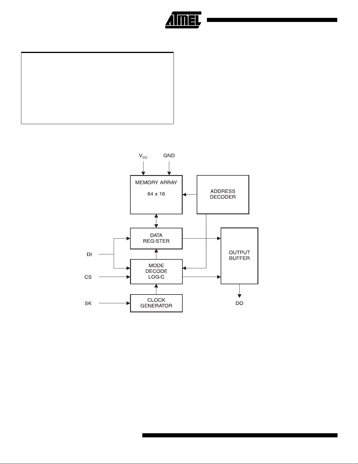
The AT93C46B is enabled through the Chip S elect pin (CS) , and accessed vi a a 3wire serial interface consisting of Data Input (DI), Data Output (DO), and Shift Clock
(SK). Upon receiving a READ instruction at DI, the address is decoded and the data is
clocked out serially on the data output pin DO. The WRITE cycle is compl etely selftimed and no separate ERASE cycle is required before WRITE. The WRITE cycle is
only enabled when the part is in the ERASE/WRITE ENABLE state. When CS is
brought “high” fol lowing the in itiation of a WRITE cycle, the DO pin o utputs the
READY/BUSY status of the part.
The AT93C46B is available in 4.5V to 5.5V, 2.7V to 5.5V, and 2.5V to 5.5V versions.
AT93C46B
3-Wire
Serial
2
E
PROMs
1K (64 x 16)
AT93C46B
Pin Configuration
Pin Name Function
CS Chip Select
SK Serial Data Clock
DI Serial Data Input
DO Serial Data Output
GND Ground
V
CC
NC No Connect
Power Supply
CS
SK
DI
DO
CS
SK
DI
SO
8-Pin PDIP
1
2
3
4
8-Pin SOIC
1
2
3
4
8
VCC
7
NC
6
NC
5
GND
8
VCC
7
NC
6
NC
5
GND
0917A-A–11/97
1
Absolute Maximum Ratings*
Operating Temperature.........................-55°C to +125°C
Storage Temperature............................-65°C to +150°C
Voltage on Any Pin
with Respect to Ground........................... -1.0V to +7.0V
Maximum Operating Voltage.................................6.25V
DC Output Current ..............................................5.0 mA
Block Diagram
*NOTICE: Stresses beyond those listed under “Absolute
Maximum Ratings” may cause permanent damage to the dev ice . This is a s tress rating only an d
functional oper ation of the de vice at these or any
other conditions beyond those indicated in the
operational sections of this specification is not
implied. Exposure to absolute maximum rating
conditions f or e xtended periods ma y af fect de vice
reliability .
2
AT93C46B
AT93C46B
Pin Capacitance
(1)
Applicable over recommended operating range from TA = 25°C, f = 1.0 MHz, VCC = +5.0V (unless otherwise noted).
Test Conditions Max Units Conditions
C
C
Output Capacitance (DO ) 5 pF V
OUT
Input Capacitance (CS, SK, DI) 5 pF VIN = 0V
IN
OUT
= 0V
Note: 1. This parameter is characterized and is not 100% tested.
DC Characteristics
Applicable over recommended operating range from: TAI = -40°C to +85°C, VCC = +2.5V to +5.5V,
= 0°C to +70°C, VCC = +2.5V to +5.5V (unless otherwise noted).
T
AC
Symbol Parameter T est Condition Min T yp Max Units
V
V
V
I
CC2
CC3
CC4
CC
Supply Voltage 2.5 5.5 V
Supply Voltage 2.7 5.5 V
Supply Voltage 4.5 5.5 V
READ at 1.0 MHz 0.5 2.0 mA
Supply Current VCC = 5.0V
WRITE at 1.0 MHz 0.5 2.0 mA
I
SB1
I
SB2
I
SB3
I
IL
I
OL
V
V
V
V
V
V
V
V
IL1
IH1
IL2
IH2
OL1
OH1
OL2
OH2
Standby Current VCC = 2.5V CS = 0V 14.0 20.0
Standby Current VCC = 2.7V CS = 0V 14.0 20.0
Standby Current VCC = 5.0V CS = 0V 35.0 50.0
Input Leakage VIN = 0V to VCC 0.1 1.0
Output Leakage VIN = 0V to VCC 0.1 1.0
(1)
Input Low Voltage
(1)
Input High Voltage
(1)
Input Low Voltage
(1)
Input High Voltage
Output Low Voltage
Output High Voltage
Output Low Voltage
Output High Voltage
4.5V ≤ V
1.8V ≤ V
4.5V ≤ V
1.8V ≤ V
≤ 5.5V
CC
≤ 2.7V
CC
≤ 5.5V
CC
≤ 2.7V
CC
Note: 1. VIL and VIH max are reference only and are not tested.
-0.1
2.0
0.0
x 0.7
V
CC
I
= 2.1 mA 0.4 V
OL
I
= -0.4 mA 2.4 V
OH
I
= 0.15 mA 0.2 V
OL
I
= -100 µAV
OH
- 0.2 V
CC
0.8
+ 1
V
CC
V
x 0.3
CC
+ 1
V
CC
µ
A
µ
A
µ
A
µ
A
µ
A
V
V
3

AC Characteristics
Applicable over recommended operating range from TA = -40°C to + 85°C, VCC = +2.5V to + 5.5V,
= 1 TTL Gate and 100 pF (unless otherwise noted).
C
L
Symbol Parameter Test Condition Min Typ Max Units
IL
≤ 5.5V
CC
≤ 5.5V
CC
≤ 5.5V
CC
≤ 5.5V
CC
≤ 5.5V
CC
≤ 5.5V
CC
≤ 5.5V
CC
≤ 5.5V
CC
≤ 5.5V
CC
≤ 5.5V
CC
≤ 5.5V
CC
≤ 5.5V
CC
4.5V ≤ V
2.7V ≤ V
2.5V ≤ V
4.5V ≤ V
2.7V ≤ V
2.5V ≤ V
4.5V ≤ V
2.7V ≤ V
2.5V ≤ V
4.5V ≤ V
2.7V ≤ V
2.5V ≤ V
4.5V ≤ V
2.7V ≤ V
2.5V ≤ V
4.5V ≤ V
2.7V ≤ V
2.5V ≤ V
≤ 5.5V
CC
≤ 5.5V
CC
≤ 5.5V
CC
≤ 5.5V
CC
≤ 5.5V
CC
≤ 5.5V
CC
≤ 5.5V
CC
≤ 5.5V
CC
≤ 5.5V
CC
≤ 5.5V
CC
≤ 5.5V
CC
≤ 5.5V
CC
≤ 5.5V
CC
≤ 5.5V
CC
≤ 5.5V
CC
≤ 5.5V
CC
≤ 5.5V
CC
≤ 5.5V
CC
4.5V ≤ VCC ≤ 5.5V
2.7V ≤ V
2.5V ≤ V
≤ 5.5V
CC
≤ 5.5V
CC
0
0
0
250
250
500
250
250
500
250
250
500
50
50
100
100
100
200
100
100
200
2
1
0.5
250
250
500
250
250
500
250
250
500
100
100
200
0.1 10 ms
4.5V ≤ V
= 5.0V, Page Mode 1M Cycles
CC
≤ 5.5V 1 ms
CC
MHz
4.5V ≤ V
f
SK
SK Clock Frequency
2.7V ≤ V
2.5V ≤ V
4.5V ≤ V
t
SKH
SK High Time
2.7V ≤ V
2.5V ≤ V
4.5V ≤ V
t
SKL
SK Low Time
2.7V ≤ V
2.5V ≤ V
4.5V ≤ V
t
CS
Minimum CS Low Time
2.7V ≤ V
2.5V ≤ V
t
CSS
t
DIS
t
CSH
t
DIH
t
PD1
t
PD0
t
SV
t
DF
t
WP
CS Setup Time Relative to SK
DI Setup Time Relative to SK
CS Hold Time Relative to SK 0 ns
DI Hold Time Relative to SK
Output Delay to ‘1’ AC Test
Output Delay to ‘0’ AC Test
CS to Status Valid AC Test
CS to DO in High Impedance
AC Test
CS = V
Write Cycle Time
Endurance 25°C, V
ns
ns
ns
ns
ns
ns
ns
ns
ns
ns
4
AT93C46B

Instruction Set for the AT93C46B
Instruction SB Op Code
AT93C46B
Address
(x16) Comments
READ 1 10 A
EWEN 1 00 11XXXX Write enable must precede all programming modes.
ERASE 1 11 A
WRITE 1 01 A
ERAL 1 00 10XXXX Erases all memory locations. Valid only at VCC = 4.5V to 5.5V.
WRAL 1 00 01XXXX Writes all memory locations. Valid only at V
EWDS 1 00 00XXXX Disables all programming instructions.
5
5
5
- A
- A
- A
0
0
0
Reads data stored in memory, at specified address.
Erase memory location An - A0.
Writes memory location An - A0.
= 4.5V to 5.5V.
CC
5

Functional Description
The AT93C46B is accessed via a simple and versatile
three-wire serial communication interface. Device operation is controll ed by s even in structions issu ed by the host
processor. A valid instruction starts with a rising edge of CS
and consists of a Sta rt Bit (logi c ‘1’) foll owed by the appropriate Op Code and the desired memory Address location.
READ (READ):
the Address code fo r th e m emo ry loc at ion to b e r ea d. Aft er
the instruction and address are decoded, data from the
selected memory location is available at the serial output
pin DO. Output data changes are synchronized with the rising edges of serial clock SK. It should be noted that a
dummy bit (logic ‘0’) precedes the 16 bit data output string.
ERASE/WRITE (EWEN):
part automatically goes into the Erase/Write Disable
(EWDS) state when power is first applied. An Erase/Write
Enable (EWEN) instruction must be executed first before
any programming instructions can be carried out. Please
note that once in the Erase/Write Enable state, programming remains enabled un til an Erase/Write Disable
(EWDS) instruc tion is executed o r V
from the part.
ERASE (ERASE):
grams all bits in the specified memory location to the logical
‘1’ state. The self-timed erase cycle starts once the ERASE
instruction and address are decoded. The DO pin outputs
the READY / BUSY status of t he part if CS is brough t high
after being kept low for a minimum of 250 ns (t
‘1’ at pin DO indicates that the selected memory location
has been erased, and the part is ready for another instruction.
Synchronous Data Timing
The Read (READ) instruction contains
To assure data integrity, the
power is removed
CC
The Erase (ERASE) instruction pro-
). A logic
CS
WRITE (WRITE):
The Write (WRITE) instruc tio n con tai ns
the 16 bits of data to be written into the specified memory
location. The self-timed programming cycle starts after the
last bit of data is received at serial data input pin DI. The
DO pin outputs the READY/BUSY status of the part if CS is
brought high after being kept low for a minimum of 250 ns
). A logic ‘0’ at DO in dicate s that prog ramm ing is still in
(t
CS
progress. A logic ‘1’ indicates that the memory l ocation at
the specified address has been written with the data pattern contained in the instruction and the part is ready for
further instructions.
ERASE ALL (ERAL):
The Erase All (ERAL) instruction
programs every bit in the memory array to the logic ‘1’ state
and is primarily u sed for test ing pur pose s. The DO pin ou tputs the READ Y/BUSY statu s of t he part i f CS i s brou ght
high after being kept low for a minimum of 250 ns (t
ERAL instruction is valid only at V
WRITE ALL (WRAL):
The Write All (WRAL) instruction
= 5.0V ± 10%.
CC
CS
). The
programs all memory locations with the data patterns specified in the instruction. The DO pin outputs the
READY/BUSY stat us of th e p art if C S is br ough t hi gh a fter
being kept low for a minimum of 25 0 ns (t
instruction is valid only at V
= 5.0V ± 10%.
CC
ERASE/WRITE DI SABLE (EWDS) :
). The WRAL
CS
To protect against
accidental data disturb, the Erase/Write Disable (EWDS)
instruction disables all programming modes and should be
executed after all programming operations. The operation
of the READ instruction is independent of both the EWEN
and EWDS instructions and can be executed at any time.
Note: 1. This is the minimum SK period.
6
AT93C46B

Organization Key for Timing Diagrams
I/O
A
N
D
N
READ Timing
AT93C46B
(x16)
A
5
D
15
AT93C46B
EWEN Timing
EWDS Timing
Note: 1. Requires a minimum of nine clock cycles.
(1)
7

WRITE Timing
WRAL Timing
Notes: 1. Valid only at VCC = 4.5V to 5.5V.
ERASE Timing
(1)(2)
2. Requires a minimum of nine clock cycles.
8
AT93C46B

AT93C46B
TERAL Timing
Note: 1. Valid only at VCC = 4.5V to 5.5V.
(1)
9
Ordering Information
tWP (max)
(ms)
10 2000 50.0 2000
10 800 20.0 1000
10 600 20.0 500
10 2000 50.0 2000
10 800 20.0 1000
10 600 20.0 500
ICC (max)
(µA)
ISB (max)
(µA)
f
MAX
(kHz) Ordering Code Package Operation Range
AT93C46B-10PC
AT93C46B-10SC
AT93C46B-10PC-2.7
AT93C46B-10SC-2.7
AT93C46B-10PC-2.5
AT93C46B-10SC-2.5
AT93C46B-10PI
AT93C46B-10SI
AT93C46B-10PI-2.7
AT93C46B-10SI-2.7
AT93C46B-10PI-2.5
AT93C46B-10SI-2.5
8P3
8S1
8P3
8S1
8P3
8S1
8P3
8S1
8P3
8S1
8P3
8S1
Commercial
(0°C to 70°C)
Commercial
(0°C to 70°C)
Commercial
(0°C to 70°C)
Industrial
(-40°C to 85°C)
Industrial
(-40°C to 85°C)
Industrial
(-40°C to 85°C)
Package Type
8P3 8 Lead, 0.300" Wide, Plastic Dual Inline Package (PDIP)
8S1 8 Lead, 0.150" Wide, Plastic Gull Wing Small Outline (JEDEC SOIC)
Options
Blank Standard Device (4.5V to 5.5V)
-2.7 Low Voltage (2.7V to 5.5V)
-2.5 Low Voltage (2.5V to 5.5V)
10
AT93C46B
 Loading...