


BDTIC www.bdtic.com/ATMEL
Features
• Incorporates the ARM926EJ-S
– DSP instruction Extensions, ARM Jazelle
– 8 Kbyte Data Cache, 16 Kbyte Instruction Cache, Write Buffer
– 200 MIPS at 180 MHz
– Memory Management Unit
– EmbeddedICE
• Additional Embedded Memories
– One 32 Kbyte Internal ROM, Single-cycle Access at Maximum Matrix Speed
– One 32 Kbyte (for AT91SAM9XE256 and AT91SAM9XE512) or 16 Kbyte (for
AT91SAM9XE128) Internal SRAM, Single-cycle Access at Maximum Matrix Speed
– 128, 256 or 512 Kbytes of Internal High-speed Flash for AT91SAM9XE128,
AT91SAM9XE256 or AT91SAM9XE512 Respectively. Organized in 256, 512 or 1024
Pages of 512 Bytes Respectively.
• 128-bit Wide Access
• Fast Read Time: 60 ns
• Page Programming Time: 4 ms, Including Page Auto-erase,
Full Erase Time: 10 ms
• 10,000 Write Cycles, 10 Years Data Retention, Page Lock Capabilities, Flash
Security Bit
• Enhanced Embedded Flash Controller (EEFC)
– Interface of the Flash Block with the 32-bit Internal Bus
– Increases Performance in ARM and Thumb Mode with 128-bit Wide Memory
Interface
• External Bus Interface (EBI)
– Supports SDRAM, Static Memory, ECC-enabled NAND Flash and CompactFlash
• USB 2.0 Full Speed (12 Mbits per second) Device Port
– On-chip Transceiver, 2,688-byte Configurable Integrated DPRAM
• USB 2.0 Full Speed (12 Mbits per second) Host Single Port in the 208-pin PQFP Device
and Double Port in 217-ball LFBGA Device
– Single or Dual On-chip Transceivers
– Integrated FIFOs and Dedicated DMA Channels
• Ethernet MAC 10/100 Base-T
– Media Independent Interface or Reduced Media Independent Interface
– 28-byte FIFOs and Dedicated DMA Channels for Receive and Transmit
• Image Sensor Interface
– ITU-R BT. 601/656 External Interface, Programmable Frame Capture Rate
– 12-bit Data Interface for Support of High Sensibility Sensors
– SAV and EAV Synchronization, Preview Path with Scaler, YCbCr Format
• Bus Matrix
– Six 32-bit-layer Matrix
– Remap Command
• Fully-featured System Controller, including
– Reset Controller, Shutdown Controller
– Four 32-bit Battery Backup Registers for a Total of 16 Bytes
– Clock Generator and Power Management Controller
– Advanced Interrupt Controller and Debug Unit
– Periodic Interval Timer, Watchdog Timer and Real-time Timer
™
, Debug Communication Channel Support
™
ARM® Thumb® Processor
®
Technology for Java® Acceleration
™
AT91 ARM
Thumb
Microcontrollers
AT91SAM9XE128
AT91SAM9XE256
AT91SAM9XE512
Preliminary
6254A–ATARM–01-Feb-08

• Reset Controller (RSTC)
– Based on a Power-on Reset Cell, Reset Source Identification and Reset Output Control
• Clock Generator (CKGR)
– Selectable 32,768 Hz Low-power Oscillator or Internal Low Power RC Oscillator on Battery Backup Power Supply,
Providing a Permanent Slow Clock
– 3 to 20 MHz On-chip Oscillator, One Up to 240 MHz PLL and One Up to 100 MHz PLL
• Power Management Controller (PMC)
– Very Slow Clock Operating Mode, Software Programmable Power Optimization Capabilities
– Two Programmable External Clock Signals
• Advanced Interrupt Controller (AIC)
– Individually Maskable, Eight-level Priority, Vectored Interrupt Sources
– Three External Interrupt Sources and One Fast Interrupt Source, Spurious Interrupt Protected
• Debug Unit (DBGU)
– 2-wire UART and support for Debug Communication Channel, Programmable ICE Access Prevention
• Periodic Interval Timer (PIT)
– 20-bit Interval Timer Plus 12-bit Interval Counter
• Watchdog Timer (WDT)
– Key-protected, Programmable Only Once, Windowed 16-bit Counter Running at Slow Clock
• Real-Time Timer (RTT)
– 32-bit Free-running Backup Counter Running at Slow Clock with 16-bit Prescaler
• One 4-channel 10-bit Analog to Digital Converter
• Three 32-bit Parallel Input/Output Controllers (PIOA, PIOB, PIOC,)
– 96 Programmable I/O Lines Multiplexed with up to Two Peripheral I/Os
– Input Change Interrupt Capability on Each I/O Line
– Individually Programmable Open-drain, Pull-up Resistor and Synchronous Output
• Peripheral DMA Controller Channels (PDC)
• Two-slot Multimedia Card Interface (MCI)
™
– SDCard/SDIO and MultiMediaCard
– Automatic Protocol Control and Fast Automatic Data Transfers with PDC
Compliant
• One Synchronous Serial Controllers (SSC)
– Independent Clock and Frame Sync Signals for Each Receiver and Transmitter
– I²S Analog Interface Support, Time Division Multiplex Support
– High-speed Continuous Data Stream Capabilities with 32-bit Data Transfer
• Four Universal Synchronous/Asynchronous Receiver Transmitters (USART)
®
– Individual Baud Rate Generator, IrDA
– Support for ISO7816 T0/T1 Smart Card, Hardware Handshaking, RS485 Support
– Full Modem Signal Control on USART0
Infrared Modulation/Demodulation
• One 2-wire UART
• Two Master/Slave Serial Peripheral Interface (SPI)
– 8- to 16-bit Programmable Data Length, Four External Peripheral Chip Selects
– Synchronous Communications
• Two Three-channel 16-bit Timer/Counters (TC)
– Three External Clock Inputs, Two Multi-purpose I/O Pins per Channel
– Double PWM Generation, Capture/Waveform Mode, Up/Down Capability
– High-Drive Capability on Outputs TIOA0, TIOA1, TIOA2
• Two Two-wire Interfaces (TWI)
– Master, Multi-master and Slave Mode Operation
– General Call Supported in Slave Mode
– Connection to PDC Channel to Optimize Data Transfers in Master Mode Only
2
AT91SAM9XE128/256/512 Preliminary
6254A–ATARM–01-Feb-08

AT91SAM9XE128/256/512 Preliminary
®
• IEEE
• Required Power Supplies:
• Available in a 208-pin PQFP Green and a 217-ball LFBGA Green Package
1. AT91SAM9XE128/256/512 Description
The AT91SAM9XE128/256/512 is based on the integration of an ARM926EJ-S processor with
fast ROM and RAM, 128, 256 or 512 Kbytes of Flash and a wide range of peripherals.
The embedded Flash memory can be programmed in-system via the JTAG-ICE interface or via
a parallel interface on a production programmer prior to mounting. Built-in lock bits and a security bit protect the firmware from accidental overwrite and preserves its confidentiality.
The AT91SAM9XE128/256/512 embeds an Ethernet MAC, one USB Device Port, and a USB
Host Controller. It also integrates several standard peripherals, like USART, SPI, TWI, Timer
Counters, Synchronous Serial Controller, ADC and a MultiMedia Card Interface.
The AT91SAM9XE128/256/512 system controller includes a reset controller capable of managing the power-on sequence of the microcontroller and the complete system. Correct device
operation can be monitored by a built-in brownout detector and a watchdog running off an integrated RC oscillator.
1149.1 JTAG Boundary Scan on All Digital Pins
– 1.65V to 1.95V for VDDBU, VDDCORE and VDDPLL
– 1.65V to 3.6V for VDDIOP1 (Peripheral I/Os)
– 3.0V to 3.6V for VDDIOP0 and VDDANA (Analog-to-digital Converter)
– Programmable 1.65V to 1.95V or 3.0V to 3.6V for VDDIOM (Memory I/Os)
The AT91SAM9XE128/256/512 is architectured on a 6-layer matrix, allowing a maximum internal bandwidth of six 32-bit buses. It also features an External Bus Interface capable of
interfacing with a wide range of memory devices.
The pinout and ball-out are fully compatible with the AT91SAM9260 with the exception that the
pin BMS is replaced by the pin ERASE.
6254A–ATARM–01-Feb-08
3
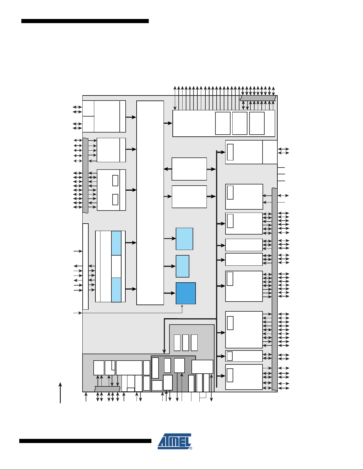
2. AT91SAM9XE128/256/512 Block Diagram
The block diagram shows all the features for the 217-LFBGA package. Some functions are not
accessible in the 208-PQFP package and the unavailable pins are highlighted in “Multiplexing
on PIO Controller A” on page 39, “Multiplexing on PIO Controller B” on page 40, “Multiplexing on
PIO Controller C” on page 41. The USB Host Port B is also not available. Table 2-1 on page 4
defines all the multiplexed and not multiplexed pins not available in the 208-PQFP package.
Table 2-1. Unavailable Signals in 208-pin PQFP Device
PIO Peripheral A Peripheral B
- HDPB -
- HDMB -
PA30 SCK2 RXD4
PA 31 S C K 0 T X D4
PB12 TWD1 ISI_D10
PB13 TWCK1 ISI_D11
PC2 AD2 PCK1
PC3 AD3 SPI1_NPCS3
PC12 IRQ0 NCS7
4
AT91SAM9XE128/256/512 Preliminary
6254A–ATARM–01-Feb-08
AT91SAM9XE128/256/512 Preliminary
Figure 2-1. AT91SAM9XE128/256/512 Block Diagram
HDMB
HDPB
HDMA
HDPA
ISI_HSYNC
ISI_DO-ISI_D7
ISI_PCK
ISI_MCK
ISI_VSYNC
Transc.
Transc.
USB
OHCI
Image
Sensor
Interface
DMA
DMA
D0-D15
A0/NBS0
A2-A15, A18-A20
A1/NBS2/NWR2
EBI
A16/BA0
A17/BA1
NCS0
NCS1/SDCS
NAND Flash
CompactFlash
NRD
NWR0/NWE
NWR1/NBS1
NWR3/NBS3
SDCK, SDCKE
RAS, CAS
SDWE, SDA10
NANDOE, NANDWE
A21/NANDALE
A22/NANDCLE
Static
SDRAM
Controller
DPRAM
D16-D31
NWAIT
Memory
Controller
USB
Device
A23-A24
NCS5/CFCS1
A25/CFRNW
NCS4/CFCS0
ECC
Controller
NCS2, NCS6, NCS7
NCS3/NANDCS
CFCE1-CFCE2
Transceiver
DDP
DDM
F100
MDIO
MDC
ETX0-ETX3
ERX0-ERX3
ERXER-ERXDV
ECRS-ECOL
ETXEN-ETXER
ETXCK-ERXCK
JTAGSEL
RTCK
TCK
TMS
TDO
TDI
NTRST
ERASE
SLAVEMASTER
JTAG Selection and Boundary Scan
System
Controller
10/100 Ethernet
In-Circuit Emulator
AIC
FIFO
MAC
FIFO
DCache
8 Kbytes
MMU
ARM926EJ-S Processor
ICache
16 Kbytes
PDC
DBGU
Peripheral
24-channel
DMA
Bridge
Peripheral
6-layer Matrix
Kbytes
16 or 32
Fast SRAM
ROM
RTT
OSC
Flash
PIOA
SHDC
32 Kbytes
or 512
128, 256
PIOB
Bus Interface
ID
PLLB
Filter
OSC
PITWDT
4GPREG
RC
PMC
PLLA
DMA
Kbytes
PIOC
POR
RSTC
POR
BOD
APB
PDC
PDC
PDC
PDC
PDC
PDC
4-channel
10-bit ADC
SSC
TC3
TC4
TC0
TC1
SPI0
SPI1
USART0
USART1
USART2
TWI0
TWI1
MCI
TC5
TC2
USART3
GNDANA
VDDANA
ADVREF
ADTRIG
AD0-AD3
RK
RF
RD
TD
TF
TK
TIOB3-TIOB5
TIOA3-TIOA5
TCLK3-TCLK5
TIOB0-TIOB2
TIOA0-TIOA2
MISO
TCLK0-TCLK2
MOSI
SPCK
NPCS0
NPCS1
NPCS2
NPCS3
SPI0_, SPI1_
DTR0
RI0
DCD0
DSR0
USART4
TWCK
TWD
MCCK
MCCDA
MCCDB
TXD0-TXD5
RXD0-RXD5
SCK0-SCK3
RTS0-RTS3
CTS0-CTS3
MCDA0-MCDA3
6254A–ATARM–01-Feb-08
TST
FIQ
IRQ0-IRQ2
DTXD
DRXD
PLLRCA
PCK0-PCK1
XIN
XOUT
XIN32
XOUT32
OSCSEL
SHDN
WKUP
VDDBU
NRST
MCDB0-MCDB3
VDDCORE
5

3. Signals Description
Table 3-1 gives details on the signal name classified by peripheral.
Table 3-1. Signal Description List
Active
Signal Name Function Type
Power Supplies
VDDIOM EBI I/O Lines Power Supply Power 1.65V to 1.95V or 3.0V to 3.6V
VDDIOP0 Peripherals I/O Lines Power Supply Power 3.0V to 3.6V
VDDIOP1 Peripherals I/O Lines Power Supply Power 1.65V to 3.6V
VDDBU Backup I/O Lines Power Supply Power 1.65V to 1.95V
VDDANA Analog Power Supply Power 3.0V to 3.6V
VDDPLL PLL Power Supply Power 1.65V to 1.95V
VDDCORE
GND Ground Ground
GNDPLL PLL Ground Ground
GNDANA Analog Ground Ground
GNDBU Backup Ground Ground
XIN Main Oscillator Input Input
XOUT Main Oscillator Output Output
XIN32 Slow Clock Oscillator Input Input
XOUT32 Slow Clock Oscillator Output Output
OSCSEL Slow Clock Oscillator Selection Input
PLLRCA PLL A Filter Input
PCK0 - PCK1 Programmable Clock Output Output
SHDN Shutdown Control Output
WKUP Wake-Up Input Input
NTRST Test Reset Signal Input Low Pull-up resistor
TCK Test Clock Input No pull-up resistor
TDI Test Data In Input No pull-up resistor
TDO Test Data Out Output
TMS Test Mode Select Input No pull-up resistor
JTAGSEL JTAG Selection Input
RTCK Return Test Clock Output
Core Chip and Embedded Memories
Power Supply
Clocks, Oscillators and PLLs
Shutdown, Wakeup Logic
ICE and JTAG
Power 1.65V to 1.95V
Level Comments
Accepts between 0V and
VDDBU.
Driven at 0V only. Do not tie
over VDDBU.
Accepts between 0V and
VDDBU.
Pull-down resistor. Accepts
between 0V and VDDBU.
6
AT91SAM9XE128/256/512 Preliminary
6254A–ATARM–01-Feb-08

AT91SAM9XE128/256/512 Preliminary
Table 3-1. Signal Description List (Continued)
Active
Signal Name Function Type
Flash Memory
ERASE
NRST Microcontroller Reset I/O Low Pull-up resistor
TST Test Mode Select Input
DRXD Debug Receive Data Input
DTXD Debug Transmit Data Output
IRQ0 - IRQ2 External Interrupt Inputs Input
FIQ Fast Interrupt Input Input
PA0 - PA31 Parallel IO Controller A I/O Pulled-up input at reset
PB0 - PB30 Parallel IO Controller B I/O Pulled-up input at reset
PC0 - PC31 Parallel IO Controller C I/O Pulled-up input at reset
D0 - D31 Data Bus I/O Pulled-up input at reset
A0 - A25 Address Bus Output 0 at reset
NWAIT External Wait Signal Input Low
NCS0 - NCS7 Chip Select Lines Output Low
NWR0 - NWR3 Write Signal Output Low
NRD Read Signal Output Low
NUB Upper Byte Select Output Low
NLB Lower Byte Select Output Low
NWE Write Enable Output Low
NBS0 - NBS3 Byte Mask Signal Output Low
CFCE1 - CFCE2 CompactFlash Chip Enable Output Low
CFOE CompactFlash Output Enable Output Low
CFWE CompactFlash Write Enable Output Low
CFIOR CompactFlash IO Read Output Low
CFIOW CompactFlash IO Write Output Low
CFRNW CompactFlash Read Not Write Output
CFCS0 - CFCS1 CompactFlash Chip Select Lines Output Low
Flash and NVM Configuration Bits
Erase Command
Reset/Test
Debug Unit - DBGU
Advanced Interrupt Controller - AIC
PIO Controller - PIOA - PIOB - PIOC
External Bus Interface - EBI
Static Memory Controller - SMC
CompactFlash Support
Input High Pull-down resistor
Level Comments
Pull-down resistor. Accepts
between 0V and VDDBU.
6254A–ATARM–01-Feb-08
7

Table 3-1. Signal Description List (Continued)
Active
Signal Name Function Type
NAND Flash Support
NANDCS NAND Flash Chip Select Output Low
NANDOE NAND Flash Output Enable Output Low
NANDWE NAND Flash Write Enable Output Low
SDRAM Controller
SDCK SDRAM Clock Output
SDCKE SDRAM Clock Enable Output High
SDCS SDRAM Controller Chip Select Output Low
BA0 - BA1 Bank Select Output
SDWE SDRAM Write Enable Output Low
RAS - CAS Row and Column Signal Output Low
SDA10 SDRAM Address 10 Line Output
Multimedia Card Interface MCI
MCCK Multimedia Card Clock Output
MCCDA Multimedia Card Slot A Command I/O
MCDA0 - MCDA3 Multimedia Card Slot A Data I/O
MCCDB Multimedia Card Slot B Command I/O
MCDB0 - MCDB3 Multimedia Card Slot B Data I/O
Universal Synchronous Asynchronous Receiver Transmitter USARTx
SCKx USARTx Serial Clock I/O
TXDx USARTx Transmit Data I/O
RXDx USARTx Receive Data Input
RTSx USARTx Request To Send Output
CTSx USARTx Clear To Send Input
DTR0 USART0 Data Terminal Ready Output
DSR0 USART0 Data Set Ready Input
DCD0 USART0 Data Carrier Detect Input
RI0 USART0 Ring Indicator Input
Synchronous Serial Controller - SSC
TD SSC Transmit Data Output
RD SSC Receive Data Input
TK SSC Transmit Clock I/O
RK SSC Receive Clock I/O
TF SSC Transmit Frame Sync I/O
RF SSC Receive Frame Sync I/O
Level Comments
8
AT91SAM9XE128/256/512 Preliminary
6254A–ATARM–01-Feb-08

AT91SAM9XE128/256/512 Preliminary
Table 3-1. Signal Description List (Continued)
Active
Signal Name Function Type
Timer/Counter - TCx
TCLKx TC Channel x External Clock Input Input
TIOAx TC Channel x I/O Line A I/O
TIOBx TC Channel x I/O Line B I/O
Serial Peripheral Interface - SPIx_
SPIx_MISO Master In Slave Out I/O
SPIx_MOSI Master Out Slave In I/O
SPIx_SPCK SPI Serial Clock I/O
SPIx_NPCS0 SPI Peripheral Chip Select 0 I/O Low
SPIx_NPCS1-SPIx_NPCS3 SPI Peripheral Chip Select Output Low
Two-Wire Interface
TWDx Two-wire Serial Data I/O
TWCKx Two-wire Serial Clock I/O
USB Host Port
HDPA USB Host Port A Data + Analog
HDMA USB Host Port A Data - Analog
HDPB USB Host Port B Data + Analog
HDMB USB Host Port B Data + Analog
USB Device Port
DDM USB Device Port Data - Analog
DDP USB Device Port Data + Analog
Ethernet 10/100
ETXCK Transmit Clock or Reference Clock Input MII only, REFCK in RMII
ERXCK Receive Clock Input MII only
ETXEN Transmit Enable Output
ETX0-ETX3 Transmit Data Output ETX0-ETX1 only in RMII
ETXER Transmit Coding Error Output MII only
ERXDV Receive Data Valid Input RXDV in MII, CRSDV in RMII
ERX0-ERX3 Receive Data Input ERX0-ERX1 only in RMII
ERXER Receive Error Input
ECRS Carrier Sense and Data Valid Input MII only
ECOL Collision Detect Input MII only
EMDC Management Data Clock Output
EMDIO Management Data Input/Output I/O
EF100 Force 100Mbit/sec. Output High
Level Comments
6254A–ATARM–01-Feb-08
9
Table 3-1. Signal Description List (Continued)
Active
Signal Name Function Type
Image Sensor Interface
ISI_D0-ISI_D11 Image Sensor Data Input
ISI_MCK Image sensor Reference clock output
ISI_HSYNC Image Sensor Horizontal Synchro input
ISI_VSYNC Image Sensor Vertical Synchro input
ISI_PCK Image Sensor Data clock input
Analog to Digital Converter
AD0-AD3 Analog Inputs Analog
ADVREF Analog Positive Reference Analog
ADTRG ADC Trigger Input
Fast Flash Programming Interface
PGMEN[2:0] Programming Enabling Input
PGMNCMD Programming Command Input Low
PGMRDY Programming Ready Output High
PGMNOE Programming Read Input Low
PGMNVALID Data Direction Output Low
PGMM[3:0] Programming Mode Input
PGMD[15:0] Programming Data I/O
Level Comments
Digital pulled-up inputs at
reset
10
AT91SAM9XE128/256/512 Preliminary
6254A–ATARM–01-Feb-08

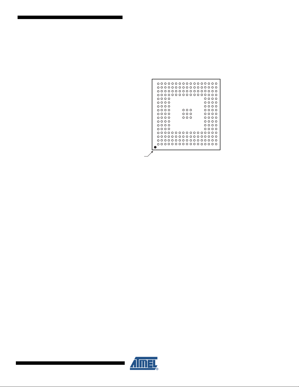
4. Package and Pinout
The AT91SAM9XE128/256/512 is available in a 208-pin PQFP Green package (0.5mm pitch) or
in a 217-ball LFBGA Green package (0.8 mm ball pitch).
4.1 208-pin PQFP Package Outline
Figure 4-1 shows the orientation of the 208-pin PQFP package.
A detailed mechanical description is given in the section “AT91SAM9XE Mechanical Characteristics” of the product datasheet.
Figure 4-1. 208-pin PQFP Package Outline (Top View)
AT91SAM9XE128/256/512 Preliminary
105156
157
208
104
53
152
6254A–ATARM–01-Feb-08
11
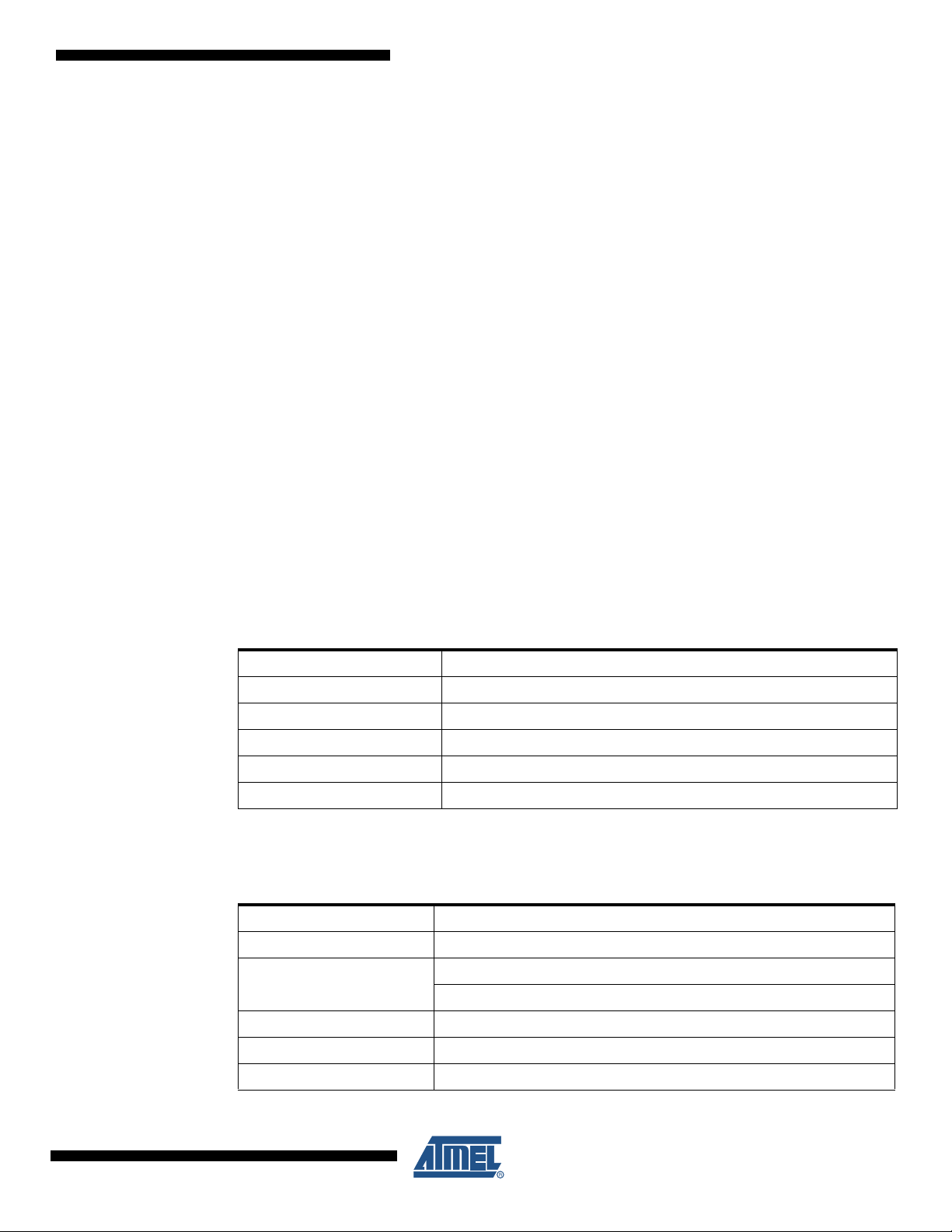
4.2 208-pin PQFP Package Pinout
Table 4-1. Pinout for 208-pin PQFP Package
Pin Signal Name Pin Signal Name Pin Signal Name Pin Signal Name
1 PA24 53 GND 105 RAS 157 ADVREF
2 PA25 54 DDM 106 D0 158 PC0
3 PA26 55 DDP 107 D1 159 PC1
4 PA27 56 PC13 108 D2 160 VDDANA
5 VDDIOP0 57 PC11 109 D3 161 PB10
6 GND 58 PC10 110 D4 162 PB11
7 PA28 59 PC14 111 D5 163 PB20
8 PA29 60 PC9 112 D6 164 PB21
9 PB0 61 PC8 113 GND 165 PB22
10 PB1 62 PC4 114 VDDIOM 166 PB23
11 PB2 63 PC6 115 SDCK 167 PB24
12 PB3 64 PC7 116 SDWE 168 PB25
13 VDDIOP0 65 VDDIOM 117 SDCKE 169 VDDIOP1
14 GND 66 GND 118 D7 170 GND
15 PB4 67 PC5 119 D8 171 PB26
16 PB5 68 NCS0 120 D9 172 PB27
17 PB6 69 CFOE/NRD 121 D10 173 GND
18 PB7 70 CFWE/NWE/NWR0 122 D11 174 VDDCORE
19 PB8 71 NANDOE 123 D12 175 PB28
20 PB9 72 NANDWE 124 D13 176 PB29
21 PB14 73 A22 125 D14 177 PB30
22 PB15 74 A21 126 D15 178 PB31
23 PB16 75 A20 127 PC15 179 PA0
24 VDDIOP0 76 A19 128 PC16 180 PA1
25 GND 77 VDDCORE 129 PC17 181 PA2
26 PB17 78 GND 130 PC18 182 PA3
27 PB18 79 A18 131 PC19 183 PA4
28 PB19 80 BA1/A17 132 VDDIOM 184 PA5
29 TDO 81 BA0/A16 133 GND 185 PA6
30 TDI 82 A15 134 PC20 186 PA7
31 TMS 83 A14 135 PC21 187 VDDIOP0
32 VDDIOP0 84 A13 136 PC22 188 GND
33 GND 85 A12 137 PC23 189 PA8
34 TCK 86 A11 138 PC24 190 PA9
35 NTRST 87 A10 139 PC25 191 PA10
36 NRST 88 A9 140 PC26 192 PA11
37 RTCK 89 A8 141 PC27 193 PA12
38 VDDCORE 90 VDDIOM 142 PC28 194 PA13
39 GND 91 GND 143 PC29 195 PA14
40 ERASE 92 A7 144 PC30 196 PA15
41 OSCSEL 93 A6 145 PC31 197 PA16
42 TST 94 A5 146 GND 198 PA17
43 JTAGSEL 95 A4 147 VDDCORE 199 VDDIOP0
44 GNDBU 96 A3 148 VDDPLL 200 GND
45 XOUT32 97 A2 149 XIN 201 PA18
46 XIN32 98 NWR2/NBS2/A1 150 XOUT 202 PA19
47 VDDBU 99 NBS0/A0 151 GNDPLL 203 VDDCORE
48 WKUP 100 SDA10 152 NC 204 GND
49 SHDN 101 CFIOW/NBS3/NWR3 153 GNDPLL 205 PA20
50 HDMA 102 CFIOR/NBS1/NWR1 154 PLLRCA 206 PA21
51 HDPA 103 SDCS/NCS1 155 VDDPLL 207 PA22
52 VDDIOP0 104 CAS 156 GNDANA 208 PA23
12
AT91SAM9XE128/256/512 Preliminary
6254A–ATARM–01-Feb-08
4.3 217-ball LFBGA Package Outline
Figure 4-2 shows the orientation of the 217-ball LFBGA package.
A detailed mechanical description is given in the section “AT91SAM9XE Mechanical Characteristics” of the product datasheet.
Figure 4-2. 217-ball LFBGA Package Outline (Top View)
AT91SAM9XE128/256/512 Preliminary
17
16
15
14
13
12
11
10
9
8
7
6
5
4
3
2
1
Ball A1
ABCDEFGHJ K LMNPRTU
6254A–ATARM–01-Feb-08
13
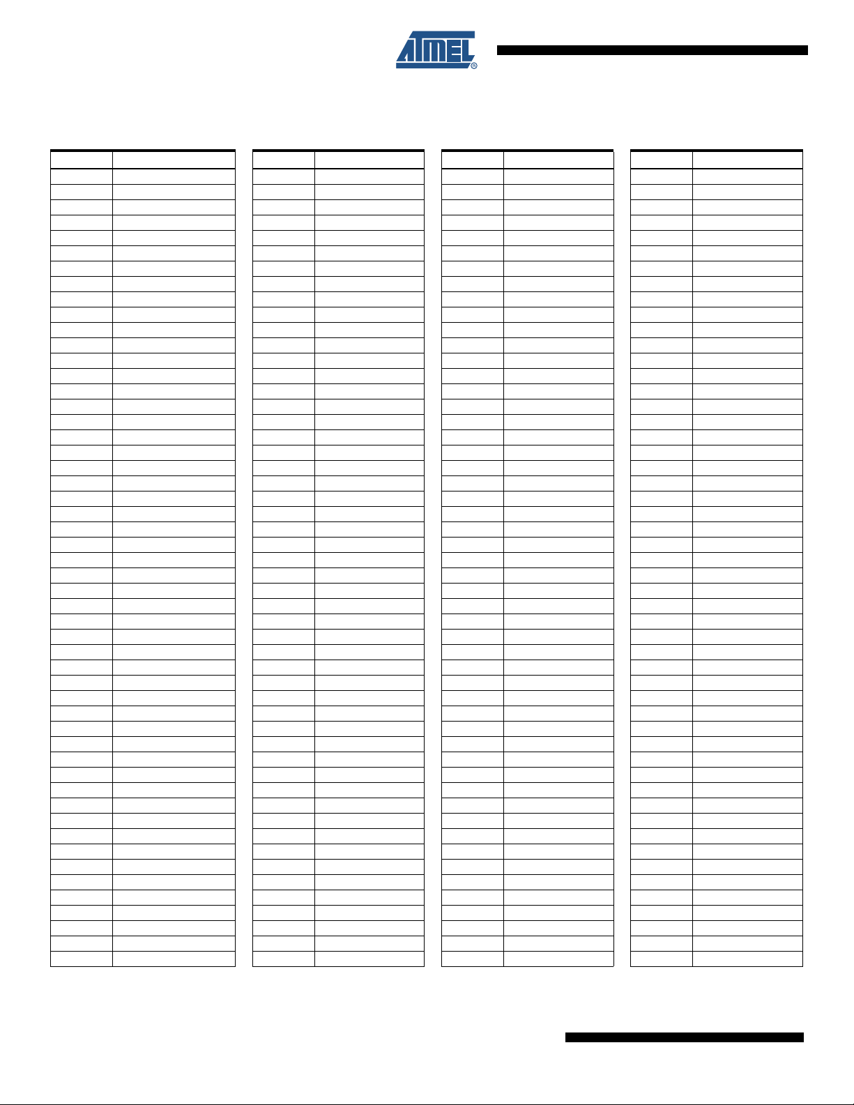
4.4 217-ball LFBGA Package Pinout
Table 4-2. Pinout for 217-ball LFBGA Package
Pin Signal Name Pin Signal Name Pin Signal Name Pin Signal Name
A1 CFIOW/NBS3/NWR3 D5 A5 J14 TDO P17 PB5
A2 NBS0/A0 D6 GND J15 PB19 R1 NC
A3 NWR2/NBS2/A1 D7 A10 J16 TDI R2 GNDANA
A4 A6 D8 GND J17 PB16 R3 PC29
A5 A8 D9 VDDCORE K1 PC24 R4 VDDANA
A6 A11 D10 GND K2 PC20 R5 PB12
A7 A13 D11 VDDIOM K3 D15 R6 PB23
A8 BA0/A16 D12 GND K4 PC21 R7 GND
A9 A18 D13 DDM K8 GND R8 PB26
A10 A21 D14 HDPB K9 GND R9 PB28
A11 A22 D15 NC K10 GND R10 PA0
A12 CFWE/NWE/NWR0 D16 VDDBU K14 PB4 R11 PA4
A13 CFOE/NRD D17 XIN32 K15 PB17 R12 PA5
A14 NCS0 E1 D10 K16 GND R13 PA10
A15 PC5 E2 D5 K17 PB15 R14 PA21
A16 PC6 E3 D3 L1 GND R15 PA23
A17 PC4 E4 D4 L2 PC26 R16 PA24
B1 SDCK E14 HDPA L3 PC25 R17 PA29
B2 CFIOR/NBS1/NWR1 E15 HDMA L4 VDDIOP0 T1 PLLRCA
B3 SDCS/NCS1 E16 GNDBU L14 PA28 T2 GNDPLL
B4 SDA10 E17 XOUT32 L15 PB9 T3 PC0
B5 A3 F1 D13 L16 PB8 T4 PC1
B6 A7 F2 SDWE L17 PB14 T5 PB10
B7 A12 F3 D6 M1 VDDCORE T6 PB22
B8 A15 F4 GND M2 PC31 T7 GND
B9 A20 F14 OSCSEL M3 GND T8 PB29
B10 NANDWE F15 ERASE M4 PC22 T9 PA2
B11 PC7 F16 JTAGSEL M14 PB1 T10 PA6
B12 PC10 F17 TST M15 PB2 T11 PA8
B13 PC13 G1 PC15 M16 PB3 T12 PA11
B14 PC11 G2 D7 M17 PB7 T13 VDDCORE
B15 PC14 G3 SDCKE N1 XIN T14 PA20
B16 PC8 G4 VDDIOM N2 VDDPLL T15 GND
B17 WKUP G14 GND N3 PC23 T16 PA22
C1 D8 G15 NRST N4 PC27 T17 PA27
C2 D1 G16 RTCK N14 PA31 U1 GNDPLL
C3 CAS G17 TMS N15 PA30 U2 ADVREF
C4 A2 H1 PC18 N16 PB0 U3 PC2
C5 A4 H2 D14 N17 PB6 U4 PC3
C6 A9 H3 D12 P1 XOUT U5 PB20
C7 A14 H4 D11 P2 VDDPLL U6 PB21
C8 BA1/A17 H8 GND P3 PC30 U7 PB25
C9 A19 H9 GND P4 PC28 U8 PB27
C10 NANDOE H10 GND P5 PB11 U9 PA12
C11 PC9 H14 VDDCORE P6 PB13 U10 PA13
C12 PC12 H15 TCK P7 PB24 U11 PA14
C13 DDP H16 NTRST P8 VDDIOP1 U12 PA15
C14 HDMB H17 PB18 P9 PB30 U13 PA19
C15 NC J1 PC19 P10 PB31 U14 PA17
C16 VDDIOP0 J2 PC17 P11 PA1 U15 PA16
C17 SHDN J3 VDDIOM P12 PA3 U16 PA18
D1 D9 J4 PC16 P13 PA7 U17 VDDIOP0
14
AT91SAM9XE128/256/512 Preliminary
6254A–ATARM–01-Feb-08

AT91SAM9XE128/256/512 Preliminary
Table 4-2. Pinout for 217-ball LFBGA Package (Continued)
Pin Signal Name Pin Signal Name Pin Signal Name Pin Signal Name
D2 D2 J8 GND P14 PA9
D3 RAS J9 GND P15 PA26
D4 D0 J10 GND P16 PA25
5. Power Considerations
5.1 Power Supplies
The AT91SAM9XE128/256/512 has several types of power supply pins:
• VDDCORE pins: Power the core, including the processor, the embedded memories and the
peripherals; voltage ranges from 1.65V and 1.95V, 1.8V nominal.
• VDDIOM pins: Power the External Bus Interface I/O lines; voltage ranges between 1.65V and
1.95V (1.8V typical) or between 3.0V and 3.6V (3.3V nominal). The expected voltage range is
selectable by software.
• VDDIOP0 pins: Power the Peripheral I/O lines and the USB transceivers; voltage ranges from
3.0V and 3.6V, 3V or 3.3V nominal.
• VDDIOP1 pin: Powers the Peripherals I/O lines involving the Image Sensor Interface; voltage
ranges from 1.65V and 3.6V, 1.8V, 2.5V, 3V or 3.3V nominal.
• VDDBU pin: Powers the Slow Clock oscillator and a part of the System Controller; voltage
ranges from 1.65V to 1.95V, 1.8V nominal.
• VDDPLL pins: Power the PLL cells and the main oscillator; voltage ranges from 1.65V and
1.95V, 1.8V nominal.
• VDDANA pin: Powers the Analog to Digital Converter; voltage ranges from 3.0V and 3.6V,
3.3V nominal.
The power supplies VDDIOM, VDDIOP0 and VDDIOP1 are identified in the pinout table and
their associated I/O lines in the multiplexing tables. These supplies enable the user to power the
device differently for interfacing with memories and for interfacing with peripherals.
Ground pins GND are common to VDDCORE, VDDIOM, VDDIOP0 and VDDIOP1 pins power
supplies. Separated ground pins are provided for VDDBU, VDDPLL and VDDANA. These
ground pins are respectively GNDBU, GNDPLL and GNDANA.
5.2 Power Consumption
The AT91SAM9XE128/256/512 consumes about 500 µA of static current on VDDCORE at
25°C. This static current rises up to 5 mA if the temperature increases to 85°C.
On VDDBU, the current does not exceed 20 µA in worst case conditions.
For dynamic power consumption, the AT91SAM9XE128/256/512 consumes a maximum of 130
mA on VDDCORE at maximum conditions (1.8V, 25°C, processor running full-performance
algorithm out of high speed memories).
5.3 Programmable I/O Lines Power Supplies
The power supplies pins VDDIOM accept two voltage ranges. This allows the device to reach its
maximum speed either out of 1.8V or 3.3V external memories.
6254A–ATARM–01-Feb-08
15

The maximum speed is 100 MHz on the pin SDCK (SDRAM Clock) loaded with 30 pF for power
supply at 1.8V and 50 pF for power supply at 3.3V. The other signals (control, address and data
signals) do not exceed 50 MHz.
The voltage ranges are determined by programming registers in the Chip Configuration registers
located in the Matrix User Interface.
At reset, the selected voltage defaults to 3.3V nominal, and power supply pins can accept either
1.8V or 3.3V. The user must program the EBI voltage range before getting the device out of its
Slow Clock Mode.
6. I/O Line Considerations
6.1 JTAG Port Pins
TMS, TDI and TCK are Schmitt trigger inputs and have no pull-up resistors.
TDO and RTCK are outputs, driven at up to VDDIOP0, and have no pull-up resistors.
The JTAGSEL pin is used to select the JTAG boundary scan when asserted at a high level (tied
to VDDBU). It integrates a permanent pull-down resistor of about 15 kΩ to GNDBU, so that it
can be left unconnected for normal operations.
The NTRST signal is described in Section 6.3.
All the JTAG signals are supplied with VDDIOP0.
6.2 Test Pin
6.3 Reset Pins
6.4 ERASE Pin
The TST pin is used for manufacturing test purposes when asserted high. It integrates a permanent pull-down resistor of about 15 kΩ to GNDBU, so that it can be left unconnected for normal
operations. Driving this line at a high level leads to unpredictable results.
This pin is supplied with VDDBU.
NRST is a bi-directional with an open-drain output integrating a non-programmable pull-up resistor. It can be driven with voltage at up to VDDIOP0.
NTRST is an input which allows reset of the JTAG Test Access port. It has no action on the
processor.
As the product integrates power-on reset cells, which manages the processor and the JTAG
reset, the NRST and NTRST pins can be left unconnected.
The NRST and NTRST pins both integrate a permanent pull-up resistor to VDDIOP0. Its value
can be found in the table “DC Characteristics” in the section “AT91SAM9XE Electrical Characteristics” in the product datasheet.
The NRST signal is inserted in the Boundary Scan.
The pin ERASE is used to re-initialize the Flash content and the NVM bits. It integrates a permanent pull-down resistor of about 15 kΩ, so that it can be left unconnected for normal operations.
16
AT91SAM9XE128/256/512 Preliminary
6254A–ATARM–01-Feb-08

This pin is debounced on the RC oscillator or 32,768 Hz to improve the glitch tolerance. Minimum debouncing time is 200 ms.
6.5 PIO Controllers
All the I/O lines are Schmitt trigger inputs and all the lines managed by the PIO Controllers integrate a programmable pull-up resistor. Refer to “DC Characteristics” in the section
“AT91SAM9XE128/256/512 Electrical Characteristics”. Programming of this pull-up resistor is
performed independently for each I/O line through the PIO Controllers.
After reset, all the I/O lines default as inputs with pull-up resistors enabled, except those which
are multiplexed with the External Bus Interface signals that require to be enabled as Peripheral
at reset. This is explicitly indicated in the column “Reset State” of the PIO Controller multiplexing
tables.
6.6 I/O Line Drive Levels
The PIO lines PA0 to PA31 and PB0 to PB31 and PC0 to PC3 are high-drive current capable.
Each of these I/O lines can drive up to 16 mA permanently with a total of 350 mA on all I/O lines.
Refer to the “DC Characteristics” section of the product datasheet.
AT91SAM9XE128/256/512 Preliminary
6.7 Shutdown Logic Pins
The SHDN pin is an output only, which is driven by the Shutdown Controller.
The pin WKUP is an input-only. It can accept voltages only between 0V and VDDBU.
6.8 Slow Clock Selection
The AT91SAM9XE128/256/512 slow clock can be generated either by an external 32,768 Hz
crystal or the on-chip RC oscillator.
The startup counter delay for the slow clock oscillator depends on the OSCSEL signal. The
32,768 Hz startup delay is 1200 ms whereas it is 200 µs for the internal RC oscillator. The pin
OSCSEL must be tied either to GNDBU or VDDBU for correct operation of the device.
Refer to the Slow Clock Selection table in the Electrical Characteristics section of the product
datasheet for the states of the OSCSEL signal.
6254A–ATARM–01-Feb-08
17

7. Processor and Architecture
7.1 ARM926EJ-S Processor
• RISC Processor Based on ARM v5TEJ Architecture with Jazelle technology for Java
acceleration
• Two Instruction Sets
– ARM High-performance 32-bit Instruction Set
– Thumb High Code Density 16-bit Instruction Set
• DSP Instruction Extensions
• 5-Stage Pipeline Architecture:
– Instruction Fetch (F)
– Instruction
– Execute (E)
– Data Memory (M)
– Register Write (W)
• 8 KB Data Cache, 16 KB Instruction Cache
– Virtually-addressed 4-way Associative Cache
– Eight words per line
– Write-through and Write-back Operation
– Pseudo-random or Round-robin Replacement
• Write Buffer
– Main Write Buffer with 16-word Data Buffer and 4-address Buffer
– DCache Write-back Buffer with 8-word Entries and a Single Address Entry
– Software Control Drain
• Standard ARM v4 and v5 Memory Management Unit (MMU)
– Access Permission for Sections
– Access Permission for large pages and small pages can be specified separately for
each quarter of the page
– 16 embedded domains
• Bus Interface Unit (BIU)
– Arbitrates and Schedules AHB Requests
– Separate Masters for both instruction and data access providing complete Matrix
system flexibility
– Separate Address and Data Buses for both the 32-bit instruction interface and the
32-bit data interface
– On Address and Data Buses, data can be 8-bit (Bytes), 16-bit (Half-words) or 32-bit
(Words)
Decode (D)
7.2 Bus Matrix
18
AT91SAM9XE128/256/512 Preliminary
• 6-layer Matrix, handling requests from 6 masters
• Programmable Arbitration strategy
– Fixed-priority Arbitration
6254A–ATARM–01-Feb-08
7.2.1 Matrix Masters
AT91SAM9XE128/256/512 Preliminary
– Round-Robin Arbitration, either with no default master, last accessed default master
or fixed default master
• Burst Management
– Breaking with Slot Cycle Limit Support
– Undefined Burst Length Support
• One Address Decoder provided per Master
– Three different slaves may be assigned to each decoded memory area: one for
internal ROM boot, one for internal flash boot, one after remap
• Boot Mode Select
– Non-volatile Boot Memory can be internal ROM or internal Flash
– Selection is made by General purpose NVM bit sampled at reset
• Remap Command
– Allows Remapping of an Internal SRAM in Place of the Boot Non-Volatile Memory
(ROM or Flash)
– Allows Handling of Dynamic Exception Vectors
The Bus Matrix of the AT91SAM9XE128/256/512 manages six Masters, thus each master can
perform an access concurrently with others, depending on whether the slave it accesses is
available.
7.2.2 Matrix Slaves
Each Master has its own decoder, which can be defined specifically for each master. In order to
simplify the addressing, all the masters have the same decodings.
Table 7-1. List of Bus Matrix Masters
Master 0 ARM926™ Instruction
Master 1 ARM926 Data
Master 2 Peripheral DMA Controller
Master 3 USB Host Controller
Master 4 Image Sensor Controller
Master 5 Ethernet MAC
Each Slave has its own arbiter, thus allowing a different arbitration per Slave to be programmed.
Table 7-2. List of Bus Matrix Slaves
Slave 0 Internal Flash
Slave 1 Internal SRAM
Internal ROM
Slave 2
USB Host User Interface
Slave 3 External Bus Interface
Slave 4 Reserved
Slave 5 Internal Peripherals
6254A–ATARM–01-Feb-08
19
7.2.3 Masters to Slaves Access
All the Masters can normally access all the Slaves. However, some paths do not make sense,
such as allowing access from the Ethernet MAC to the internal peripherals.
Thus, these paths are forbidden or simply not wired, and shown as “–” in the following table.
Table 7-3. AT91SAM9XE128/256/512 Masters to Slaves Access
Master 0 and 1 2 3 4 5
ARM926 Instruction
Slave
0 Internal Flash X – – X
1 Internal SRAM X X X X X
Internal ROM X X – – –
2
UHP User Interface X – – – –
3 External Bus Interface X X X X X
4 Reserved – ––––
Internal Peripherals X X – – –
and Data
Periphera DMA
Controller
ISI Controller Ethernet MAC USB Host
Controller
7.3 Peripheral DMA Controller
• Acting as one Matrix Master
• Allows data transfers from/to peripheral to/from any memory space without any intervention
of the processor.
• Next Pointer Support, forbids strong real-time constraints on buffer management.
• Twenty-four channels
– Two for each USART
– Two for the Debug Unit
– Two for each Serial Synchronous Controller
– Two for each Serial Peripheral Interface
– Two for the Two Wire Interface
– One for Multimedia Card Interface
– One for Analog To Digital Converter
The Peripheral DMA Controller handles transfer requests from the channel according to the following priorities (Low to High priorities):
20
– TWI0 Transmit Channel
– TWI1 Transmit Channel
– DBGU Transmit Channel
– USART4 Transmit Channel
– USART3 Transmit Channel
– USART2 Transmit Channel
– USART1 Transmit Channel
– USART0 Transmit Channel
AT91SAM9XE128/256/512 Preliminary
6254A–ATARM–01-Feb-08

AT91SAM9XE128/256/512 Preliminary
– SPI1 Transmit Channel
– SPI0 Transmit Channel
– SSC Transmit Channel
– TWI0 Receive Channel
– TWI1 Receive Channel
– DBGU Receive Channel
– USART4 Receive Channel
– USART3 Receive Channel
– USART2 Receive Channel
– USART1 Receive Channel
– USART0 Receive Channel
– ADC Receive Channel
– SPI1 Receive Channel
– SPI0 Receive Channel
– SSC Receive Channel
– MCI Transmit/Receive Channel
7.4 Debug and Test Features
• ARM926 Real-time In-circuit Emulator
– Two real-time Watchpoint Units
– Two Independent Registers: Debug Control Register and Debug Status Register
– Test Access Port Accessible through JTAG Protocol
– Debug Communications Channel
• Debug Unit
–Two-pin UART
– Debug Communication Channel Interrupt Handling
– Chip ID Register
• IEEE1149.1 JTAG Boundary-scan on All Digital Pins
6254A–ATARM–01-Feb-08
21
8. Memories
Figure 8-1. AT91SAM9XE128/256/512 Memory Mapping
0x0000 0000
0x0FFF FFFF
0x1000 0000
0x1FFF FFFF
0x2000 0000
0x2FFF FFFF
0x3000 0000
0x3FFF FFFF
0x4000 0000
0x4FFF FFFF
0x5000 0000
0x5FFF FFFF
0x6000 0000
0x6FFF FFFF
0x7000 0000
0x7FFF FFFF
0x8000 0000
0x8FFF FFFF
0x9000 0000
0xEFFF FFFF
0xF000 0000
0xFFFF FFFF
Address Memory Space
Internal Memories
EBI
Chip Select 0
EBI
Chip Select 1/
SDRAMC
EBI
Chip Select 2
EBI
Chip Select 3/
NANDFlash
EBI
Chip Select 4/
Compact Flash
Slot 0
EBI
Chip Select 5/
Compact Flash
Slot 1
EBI
Chip Select 6
EBI
Chip Select 7
Undefined
(Abort)
Internal Peripherals
256M Bytes
256M Bytes
256M Bytes
256M Bytes
256M Bytes
256M Bytes
256M Bytes
256M Bytes
256M Bytes
1,518M Bytes
256M Bytes
0x0000 0000
0x0FFF FFFF
0xF000 0000
0xFFFA 0000
0xFFFA 4000
0xFFFA 8000
0xFFFA C000
0xFFFB 0000
0xFFFB 4000
0xFFFB 8000
0xFFFB C000
0xFFFC 0000
0xFFFC 4000
0xFFFC 8000
0xFFFC C000
0xFFFD 0000
0xFFFD 4000
0xFFFD 8000
0xFFFD C000
0xFFFE 0000
0xFFFE 4000
0xFFFF C000
0xFFFF FFFF
Internal Memory Mapping
0x10 0000
0x10 8000
0x20 0000
0x28 0000
0x30 0000
0x30 8000
0x50 0000
0x50 4000
Peripheral Mapping
Reserved
TCO, TC1, TC2
TC3, TC4, TC5
Reserved
Boot Memory (1)
ROM
Reserved
Flash
Reserved
SRAM
Reserved
UHP
Reserved
UDP
MCI
TWI0
USART0
USART1
USART2
SSC
ISI
EMAC
SPI0
SPI1
USART3
USART4
TWI1
ADC
SYSC
32K Bytes
128, 256 or 512K Bytes
32K Bytes
16K Bytes
16K Bytes
16K Bytes
16K Bytes
16K Bytes
16K Bytes
16K Bytes
16K Bytes
16K Bytes
16K Bytes
16K Bytes
16K Bytes
16K Bytes
16K Bytes
16K Bytes
16K Bytes
16K Bytes
16K Bytes
16K Bytes
(1) Can be ROM or Flash
Notes :
depending on GPNVM[3]
System Controller Mapping
0xFFFF C000
0xFFFF E800
0xFFFF EA00
0xFFFF EC00
0xFFFF EE00
0xFFFF EF10
0xFFFF F000
0xFFFF F200
0xFFFF F400
0xFFFF F600
0xFFFF F800
0xFFFF FA00
0xFFFF FC00
0xFFFF FD00
0xFFFF FD10
0xFFFF FD20
0xFFFF FD30
0xFFFF FD40
0xFFFF FD50
0xFFFF FD60
0xFFFF FFFF
Reserved
ECC 512 Bytes
512 BytesSDRAMC
512 BytesSMC
MATRIX
CCFG
AIC
DBGU
PIOA
PIOB
PIOC
EEFC
PMC
RSTC
SHDC
RTTC
PITC
WDTC
GPBR
Reserved
512 Bytes
512 Bytes
512 Bytes
512 Bytes
512 bytes
512 bytes
512 bytes
256 Bytes
16 Bytes
16 Bytes
16 Bytes
16 Bytes
16 Bytes
16 Bytes
22
AT91SAM9XE128/256/512 Preliminary
6254A–ATARM–01-Feb-08

AT91SAM9XE128/256/512 Preliminary
A first level of address decoding is performed by the Bus Matrix, i.e., the implementation of the
Advanced High performance Bus (AHB) for its Master and Slave interfaces with additional
features.
Decoding breaks up the 4 Gbytes of address space into 16 banks of 256 Mbytes. The banks 1 to
7 are directed to the EBI that associates these banks to the external chip selects EBI_NCS0 to
EBI_NCS7. Bank 0 is reserved for the addressing of the internal memories, and a second level
of decoding provides 1 Mbyte of internal memory area. The bank 15 is reserved for the peripherals and provides access to the Advanced Peripheral Bus (APB).
Other areas are unused and performing an access within them provides an abort to the master
requesting such an access.
Each Master has its own bus and its own decoder, thus allowing a different memory mapping
per Master. However, in order to simplify the mappings, all the masters have a similar address
decoding.
Regarding Master 0 and Master 1 (ARM926 Instruction and Data), three different Slaves are
assigned to the memory space decoded at address 0x0: one for internal boot, one for external
boot, one after remap, refer to Table 8-3, “Internal Memory Mapping,” on page 27 for details.
A complete memory map is presented in Figure 8-1 on page 22.
8.1 Embedded Memories
8.1.1 AT91SAM9XE128
• 32 KB ROM
– Single Cycle Access at full matrix speed
• 16 KB Fast SRAM
– Single Cycle Access at full matrix speed
• 128 KB Embedded Flash
8.1.2 AT91SAM9XE256
• 32 KB ROM
– Single Cycle Access at full matrix speed
• 32 KB Fast SRAM
– Single Cycle Access at full matrix speed
• 256 KB Embedded Flash
8.1.3 AT91SAM9XE512
• 32 KB ROM
– Single Cycle Access at full matrix speed
• 32 KB Fast SRAM
– Single Cycle Access at full matrix speed
• 512 KB Embedded Flash
8.1.4 ROM Topology
6254A–ATARM–01-Feb-08
The embedded ROM contains the Fast Flash Programming and the SAM-BA boot programs.
Each of these two programs is stored at 16 KB Boundary and the program executed at address
23
zero depends on the combination of the TST pin and PA0 to PA2 pins. Figure 8-2 shows the contents of the ROM and the program available at address zero.
Figure 8-2. ROM Boot Memory Map
0x0000 0000
SAM-BA
Program
FFPI
Program
0x0000 7FFF
ROM
8.1.4.1 Fast Flash Programming Interface
The Fast Flash Programming Interface programs the device through a serial JTAG interface or a
multiplexed fully-handshaked parallel port. It allows gang-programming with market-standard
industrial programmers.
The FFPI supports read, page program, page erase, full erase, lock, unlock and protect
commands.
The Fast Flash Programming Interface is enabled and the Fast Programming Mode is entered
when the TST pin and the PA0 and PA1 pins are all tied high and PA2 is tied low.
0x0000 0000
0x0000 3FFF
SAM-BA
Program
TST=0
0x0000 0000
FFPI
Program
0x0000 3FFF
TST=1
PA0=1
PA1=1
PA2=0
8.1.4.2 SAM-BA
Table 8-1. Signal Description
Signal Name PIO Type Active Level Comments
PGMEN0 PA0 Input High Must be connected to VDDIO
PGMEN1 PA1 Input High Must be connected to VDDIO
PGMEN2 PA2 Input Low Must be connected to GND
PGMNCMD PA4 Input Low Pulled-up input at reset
PGMRDY PA5 Output High Pulled-up input at reset
PGMNOE PA6 Input Low Pulled-up input at reset
PGMNVALID PA7 Output Low Pulled-up input at reset
PGMM[3:0] PA8..PA10 Input Pulled-up input at reset
PGMD[15:0] PA12..PA27 Input/Output Pulled-up input at reset
®
Boot Assistant
The SAM-BA Boot Assistant is a default Boot Program that provides an easy way to program in
situ the on-chip Flash memory.
The SAM-BA Boot Assistant supports serial communication through the DBGU or through the
USB Device Port.
24
AT91SAM9XE128/256/512 Preliminary
6254A–ATARM–01-Feb-08

AT91SAM9XE128/256/512 Preliminary
• Communication through the DBGU supports a wide range of crystals from 3 to 20 MHz via
software auto-detection.
• Communication through the USB Device Port is depends on crystal selected:
– limited to an 18,432 Hz crystal if the internal RC oscillator is selected
– supports a wide range of crystals from 3 to 20 MHz if the 32,768 Hz crystal is
selected
The SAM-BA Boot provides an interface with SAM-BA Graphic User Interface (GUI).
8.1.5 Embedded Flash
The Flash of the AT91SAM9XE128/256/512 is organized in 256/512/1024 pages of 512 bytes
directly connected to the 32-bit internal bus. Each page contains 128 words.
The Flash contains a 512-byte write buffer allowing the programming of a page. This buffer is
write-only as 128 32-bit words, and accessible all along the 1 MB address space, so that each
word can be written at its final address.
The Flash benefits from the integration of a power reset cell and from a brownout detector to
prevent code corruption during power supply changes, even in the worst conditions.
8.1.5.1 Enhanced Embedded Flash Controller
The Enhanced Embedded Flash Controller (EEFC) is continuously clocked.
8.1.5.2 Lock Regions
The Enhanced Embedded Flash Controller (EEFC) is a slave for the bus matrix and is configurable through its User Interface on the APB bus. It ensures the interface of the Flash block with
the 32-bit internal bus. Its 128-bit wide memory interface increases performance, four 32-bit data
are read during each access, this multiply the throughput by 4 in case of consecutive data.
It also manages the programming, erasing, locking and unlocking sequences of the Flash using
a full set of commands. One of the commands returns the embedded Flash descriptor definition
that informs the system about the Flash organization, thus making the software generic programming of the access parameters of the Flash (number of wait states, timings, etc.)
The memory plane of 128, 256 or 512 Kbytes is organized in 8, 16 or 32 locked regions of 32
pages each. Each lock region can be locked independently, so that the software protects the
first memory plane against erroneous programming:
If a locked-regions erase or program command occurs, the command is aborted and the EEFC
could trigger an interrupt.
The Lock bits are software programmable through the EEFC User Interface. The command “Set
Lock Bit” enables the protection. The command “Clear Lock Bit” unlocks the lock region.
Asserting the ERASE pin clears the lock bits, thus unlocking the entire Flash.
6254A–ATARM–01-Feb-08
25
Figure 8-3. Flash First Memory Plane Mapping
0x0020 0000
Locked Regions Area
128, 256 or 512 Kbytes
256, 512 or
1024 Pages
Page 0Locked Region 0
Page 31
512 bytes
0x0021 FFFF
or 0x0023 FFFF
or 0x0027 FFFF
8.1.5.3 GPNVM Bits
8.1.5.4 Security Bit
Locked Region 7, 15 or 31
32 bits wide
16 KBytes
The AT91SAM9XE128/256/512 features four GPNVM bits that can be cleared or set respectively through the commands “Clear GPNVM Bit” and “Set GPNVM Bit” of the EEFC User
Interface.
Table 8-2. General-purpose Non volatile Memory Bits
GPNVMBit[#] Function
0 Security Bit
1 Brownout Detector Enable
2 Brownout Detector Reset Enable
3 Boot Mode Select (BMS)
The AT91SAM9XE128/256/512 features a security bit, based on a specific GPNVM bit, GPNVMBit[0]. When the security is enabled, access to the Flash, either through the ICE interface or
through the Fast Flash Programming Interface, is forbidden. This ensures the confidentiality of
the code programmed in the Flash.
26
Disabling the security bit can only be achieved by asserting the ERASE pin at 1, and after a full
Flash erase is performed. When the security bit is deactivated, all accesses to the Flash are
permitted.
As the ERASE pin integrates a permanent pull-down, it can be left unconnected during normal
operation.
AT91SAM9XE128/256/512 Preliminary
6254A–ATARM–01-Feb-08
AT91SAM9XE128/256/512 Preliminary
8.1.5.5 Non-volatile Brownout Detector Control
Two GPNVM bits are used for controlling the brownout detector (BOD), so that even after a
power loss, the brownout detector operations remain in their state.
• GPNVMBit[1] is used as a brownout detector enable bit. Setting GPNVMBit[1] enables the
BOD, clearing it disables the BOD. Asserting ERASE clears GPNVMBit[1] and thus disables
the brownout detector by default.
• GPNVMBit[2] is used as a brownout reset enable signal for the reset controller. Setting
GPNVMBit[2] enables the brownout reset when a brownout is detected, clearing
GPNVMBit[2] disables the brownout reset. Asserting ERASE disables the brownout reset by
default.
8.1.6 Boot Strategies
Table 8-3 summarizes the Internal Memory Mapping for each Master, depending on the Remap
status and the GPNVMBit[3] state at reset.
Table 8-3. Internal Memory Mapping
Address
0x0000 0000 ROM Flash SRAM
REMAP = 0 REMAP = 1
GPNVMBit[3] clear GPNVMBit[3] set
The system always boots at address 0x0. To ensure a maximum number of possibilities for boot,
the memory layout can be configured with two parameters.
REMAP allows the user to lay out the first internal SRAM bank to 0x0 to ease development. This
is done by software once the system has booted. Refer to the section “AT91SAM9XE Bus
Matrix” in the product datasheet for more details.
When REMAP = 0, a non volatile bit stored in Flash memory (GPNVMBit[3]) allows the user to
lay out to 0x0, at his convenience, the ROM or the Flash. Refer to the section “Enhanced
Embedded Flash Controller (EEFC)” in the product datasheet for more details.
Note: Memory blocks not affected by these parameters can always be seen at their specified base
addresses. See the complete memory map presented in Figure 8-1 on page 22.
The AT91SAM9XE Matrix manages a boot memory that depends on the value of GPNVMBit[3]
at reset. The internal memory area mapped between address 0x0 and 0x0FFF FFFF is reserved
for this purpose.
If GPNVMBit[3] is set, the boot memory is the internal Flash memory
If GPNVMBit[3] is clear (Flash reset State), the boot memory is the embedded ROM. After a
Flash erase, the boot memory is the internal ROM.
8.1.6.1 GPNVMBit[3] = 0, Boot on Embedded ROM
The system boots using the Boot Program.
• Boot on slow clock (On-chip RC or 32,768 Hz)
• Auto baudrate detection
• SAM-BA Boot in case no valid program is detected in external NVM, supporting
– Serial communication on a DBGU
– USB Device Port
6254A–ATARM–01-Feb-08
27

8.1.6.2 GPNVMBit[3] = 1, Boot on Internal Flash
• Boot on slow clock (On-chip RC or 32,768 Hz)
The customer-programmed software must perform a complete configuration.
To speed up the boot sequence when booting at 32 kHz, the user must take the following steps:
1. Program the PMC (main oscillator enable or bypass mode)
2. Program and start the PLL
3. Switch the main clock to the new value.
8.2 External Memories
The external memories are accessed through the External Bus Interface. Each Chip Select line
has a 256 MB memory area assigned.
Refer to the memory map in Figure 8-1 on page 22.
8.2.1 External Bus Interface
• Integrates three External Memory Controllers:
– Static Memory Controller
– SDRAM Controller
– ECC Controller
• Additional logic for NANDFlash
• Full 32-bit External Data Bus
• Up to 26-bit Address Bus (up to 64 MB linear)
• Up to 8 chip selects, Configurable Assignment:
– Static Memory Controller on NCS0
– SDRAM Controller or Static Memory Controller on NCS1
– Static Memory Controller on NCS2
– Static Memory Controller on NCS3, Optional NAND Flash support
– Static Memory Controller on NCS4 - NCS5, Optional CompactFlash support
– Static Memory Controller on NCS6-NCS7
8.2.2 Static Memory Controller
• 8-, 16- or 32-bit Data Bus
• Multiple Access Modes supported
– Byte Write or Byte Select Lines
– Asynchronous read in Page Mode supported (4- up to 32-byte page size)
• Multiple device adaptability
– Compliant with LCD Module
– Control signals programmable setup, pulse and hold time for each Memory Bank
• Multiple Wait State Management
– Programmable Wait State Generation
– External Wait Request
– Programmable Data Float Time
• Slow Clock mode supported
28
AT91SAM9XE128/256/512 Preliminary
6254A–ATARM–01-Feb-08

8.2.3 SDRAM Controller
• Supported devices:
• Numerous configurations supported
• Programming facilities
• Energy-saving capabilities
• Error detection
• SDRAM Power-up Initialization by software
• CAS Latency of 1, 2 and 3 supported
• Auto Precharge Command not used
AT91SAM9XE128/256/512 Preliminary
– Standard and Low Power SDRAM (Mobile SDRAM)
– 2K, 4K, 8K Row Address Memory Parts
– SDRAM with two or four Internal Banks
– SDRAM with 16- or 32-bit Data Path
– Word, half-word, byte access
– Automatic page break when Memory Boundary has been reached
– Multibank Ping-pong Access
– Timing parameters specified by software
– Automatic refresh operation, refresh rate is programmable
– Self-refresh, power down and deep power down modes supported
– Refresh Error Interrupt
8.2.4 Error Corrected Code Controller
• Hardware error corrected code generation
– Detection and correction by software
• Supports NAND Flash and SmartMedia devices with 8- or 16-bit data path
• Supports NAND Flash and SmartMedia with page sizes of 528,1056, 2112 and 4224 bytes
specified by software
• Supports 1 bit correction for a page of 512, 1024, 2112 and 4096 bytes with 8- or 16-bit data
path
• Supports 1 bit correction per 512 bytes of data for a page size of 512, 2048 and 4096 bytes
with 8-bit data path
• Supports 1 bit correction per 256 bytes of data for a page size of 512, 2048 and 4096 bytes
with 8-bit data path
6254A–ATARM–01-Feb-08
29

9. System Controller
The System Controller is a set of peripherals that allows handling of key elements of the system,
such as power, resets, clocks, time, interrupts, watchdog, etc.
The System Controller User Interface also embeds the registers that configure the Matrix and a
set of registers for the chip configuration. The chip configuration registers configure the EBI chip
select assignment and voltage range for external memories.
The System Controller’s peripherals are all mapped within the highest 16 KB of address space,
between addresses 0xFFFF E800 and 0xFFFF FFFF.
However, all the registers of System Controller are mapped on the top of the address space. All
the registers of the System Controller can be addressed from a single pointer by using the standard ARM instruction set, as the Load/Store instruction have an indexing mode of ±4 KB.
Figure 9-1 on page 31 shows the System Controller block diagram.
Figure 8-1 on page 22 shows the mapping of the User Interfaces of the System Controller
peripherals.
30
AT91SAM9XE128/256/512 Preliminary
6254A–ATARM–01-Feb-08

AT91SAM9XE128/256/512 Preliminary
9.1 System Controller Block Diagram
Figure 9-1. AT91SAM9XE128/256/512 System Controller Block Diagram
VDDCORE
VDDCORE
NRST
VDDBU
SHDN
WKUP
OSCSEL
XIN32
XOUT32
irq0-irq2
periph_irq[2..24]
efc2_irq
pit_irq
rtt_irq
wdt_irq
dbgu_irq
pmc_irq
rstc_irq
MCK
periph_nreset
dbgu_rxd
MCK
debug
periph_nreset
SLCK
debug
proc_nreset
cal
gpnvm[1]
BOD
POR
VDDBU
POR
SLCK
SLCK
backup_nreset
SLCK
RC
backup_nreset
OSC
SLOW
CLOCK
OSC
fiq
idle
flash_wrdis
rtt0_alarm
gpnvm[2]
por_ntrst
jtag_nreset
flash_poe
System Controller
Advanced
Interrupt
Controller
Debug
Unit
Periodic
Interval
Timer
Watchdog
Timer
bod_rst_en
Reset
Controller
Real-Time
Timer
Shutdown
Controller
wdt_fault
WDRPROC
4 General-Purpose
Backup Registers
VDDCORE Powered
por_ntrst
int
dbgu_irq
dbgu_txd
pit_irq
wdt_irq
rstc_irq
periph_nreset
proc_nreset
backup_nreset
VDDBU Powered
rtt_irq
rtt_alarm
nirq
nfiq
ntrst
proc_nreset
PCK
debug
jtag_nreset
MCK
periph_nreset
gpnvm[3]
security_bit(gpnvm0)
flash_poe
flash_wrdis
cal
gpnvm[1..3]
UHPCK
periph_clk[20]
periph_nreset
periph_irq[20]
ARM926EJ-S
Boundary Scan
TAP Controller
Bus Matrix
Embedded
Flash
USB Host
Por t
PA0-PA31
PB0-PB31
PC0-PC31
6254A–ATARM–01-Feb-08
XIN
XOUT
PLLRCA
MAIN
OSC
PLLA
PLLB
periph_nreset
periph_nreset
periph_clk[2..4]
dbgu_rxd
int
SLCK
MAINCK
PLLACK
PLLBCK
Power
Management
Controller
PIO
Controllers
periph_clk[2..27]
pck[0-1]
PCK
UDPCK
UHPCK
MCK
pmc_irq
idle
periph_irq[2..4]
irq0-irq2
fiq
dbgu_txd
UDPCK
periph_clk[10]
periph_nreset
periph_irq[10]
periph_clk[6..24]
periph_nreset
periph_irq[6..24]
in
out
enable
USB
Device
Por t
Embedded
Peripherals
31

9.2 Reset Controller
• Based on two Power-on reset cells
– One on VDDBU and one on VDDCORE
• Status of the last reset
– Either general reset (VDDBU rising), wake-up reset (VDDCORE rising), software
reset, user reset or watchdog reset
• Controls the internal resets and the NRST pin output
– Allows shaping a reset signal for the external devices
9.3 Brownout Detector and Power-on Reset
The AT91SAM9XE128/256/512 embeds one brownout detection circuit and power-on reset
cells. The power-on reset are supplied with and monitor VDDCORE and VDDBU.
Signals (flash_poe and flash_wrdis) are provided to the Flash to prevent any code corruption
during power-up or power-down sequences or if brownouts occur on the VDDCORE power
supply.
The power-on reset cell has a limited-accuracy threshold at around 1.5V. Its output remains low
during power-up until VDDCORE goes over this voltage level. This signal goes to the reset controller and allows a full re-initialization of the device.
The brownout detector monitors the VDDCORE level during operation by comparing it to a fixed
trigger level. It secures system operations in the most difficult environments and prevents code
corruption in case of brownout on the VDDCORE.
When the brownout detector is enabled and VDDCORE decreases to a value below the trigger
level (Vbot-), the brownout output is immediately activated. For more details on Vbot, see the
table “Brownout Detector Characteristics” in the section “AT91SAM9XE128/256/512 Electrical
Characteristics” in the full datasheet.
When VDDCORE increases above the trigger level (Vbot+, defined as Vbot + Vhyst), the reset
is released. The brownout detector only detects a drop if the voltage on VDDCORE stays below
the threshold voltage for longer than about 1µs.
The VDDCORE threshold voltage has a hysteresis of about 50 mV typical, to ensure spike free
brownout detection. The typical value of the brownout detector threshold is 1.55V with an accuracy of ± 2% and is factory calibrated.
The brownout detector is low-power, as it consumes less than 12 µA static current. However, it
can be deactivated to save its static current. In this case, it consumes less than 1 µA. The deactivation is configured through the GPNVMBit[1] of the Flash.
Additional information can be found in the “Electrical Characteristics” section of the product
datasheet.
9.4 Shutdown Controller
• Shutdown and Wake-Up logic
– Software programmable assertion of the SHDN pin
– Deassertion Programmable on a WKUP pin level change or on alarm
32
AT91SAM9XE128/256/512 Preliminary
6254A–ATARM–01-Feb-08

9.5 Clock Generator
Figure 9-2. Clock Generator Block Diagram
AT91SAM9XE128/256/512 Preliminary
• Embeds a low power 32,768 Hz slow clock oscillator and a low-power RC oscillator
selectable with OSCSEL signal
– Provides the permanent slow clock SLCK to the system
• Embeds the main oscillator
– Oscillator bypass feature
– Supports 3 to 20 MHz crystals
• Embeds 2 PLLs
– PLL A outputs 80 to 240 MHz clock
– PLL B outputs 70 MHz to 130 MHz clock
– Both integrate an input divider to increase output accuracy
– PLLB embeds its own filter
9.6 Power Management Controller
•Provides:
– the Processor Clock PCK
– the Master Clock MCK, in particular to the Matrix and the memory interfaces
– the USB Device Clock UDPCK
– independent peripheral clocks, typically at the frequency of MCK
– 2 programmable clock outputs: PCK0, PCK1
• Five flexible operating modes:
– Normal Mode, processor and peripherals running at a programmable frequency
OSC_SEL
XIN32
XOUT32
XIN
XOUT
PLLRCA
Clock Generator
On Chip
RC OSC
Slow Clock
Oscillator
Main
Oscillator
PLL and
Divider A
PLL and
Divider B
ControlStatus
Power
Management
Controller
Slow Clock
SLCK
Main Clock
MAINCK
PLLA Clock
PLLACK
PLLB Clock
PLLBCK
6254A–ATARM–01-Feb-08
33

– Idle Mode, processor stopped waiting for an interrupt
– Slow Clock Mode, processor and peripherals running at low frequency
– Standby Mode, mix of Idle and Backup Mode, peripheral running at low frequency,
processor stopped waiting for an interrupt
– Backup Mode, Main Power Supplies off, VDDBU powered by a battery
Figure 9-3. AT91SAM9XE128/256/512 Power Management Controller Block Diagram
Processor
SLCK
MAINCK
PLLACK
PLLBCK
Master Clock Controller
Prescaler
/1,/2,/4,...,/64
Clock
Controller
Idle Mode
Divider
/1,/2,/4
Peripherals
Clock Controller
ON/OFF
Programmable Clock Controller
PCK
int
MCK
periph_clk[..]
9.7 Periodic Interval Timer
• Includes a 20-bit Periodic Counter, with less than 1 µs accuracy
• Includes a 12-bit Interval Overlay Counter
• Real Time OS or Linux
9.8 Watchdog Timer
• 16-bit key-protected only-once-Programmable Counter
• Windowed, prevents the processor to be in a dead-lock on the watchdog access
9.9 Real-time Timer
• Real-time Timer with 32-bit free-running back-up counter
• Integrates a 16-bit programmable prescaler running on slow clock
• Alarm Register capable to generate a wake-up of the system through the Shutdown
Controller
SLCK
MAINCK
PLLACK
PLLBCK
PLLBCK
®
/WindowsCE® compliant tick generator
Prescaler
/1,/2,/4,...,/64
USB Clock Controller
Divider
/1,/2,/4
ON/OFF
ON/OFF
pck[..]
UDPCK
UHPCK
9.10 General-purpose Back-up Registers
• Four 32-bit backup general-purpose registers
34
AT91SAM9XE128/256/512 Preliminary
6254A–ATARM–01-Feb-08

9.11 Advanced Interrupt Controller
• Controls the interrupt lines (nIRQ and nFIQ) of the ARM Processor
• Thirty-two individually maskable and vectored interrupt sources
– Source 0 is reserved for the Fast Interrupt Input (FIQ)
– Source 1 is reserved for system peripherals (PIT, RTT, PMC, DBGU, etc.)
– Programmable Edge-triggered or Level-sensitive Internal Sources
– Programmable Positive/Negative Edge-triggered or High/Low Level-sensitive
• Three External Sources plus the Fast Interrupt signal
• 8-level Priority Controller
– Drives the Normal Interrupt of the processor
– Handles priority of the interrupt sources 1 to 31
– Higher priority interrupts can be served during service of lower priority interrupt
• Vectoring
– Optimizes Interrupt Service Routine Branch and Execution
– One 32-bit Vector Register per interrupt source
– Interrupt Vector Register reads the corresponding current Interrupt Vector
•Protect Mode
– Easy debugging by preventing automatic operations when protect modeIs are
enabled
•Fast Forcing
– Permits redirecting any normal interrupt source on the Fast Interrupt of the
processor
AT91SAM9XE128/256/512 Preliminary
9.12 Debug Unit
• Composed of two functions
–Two-pin UART
– Debug Communication Channel (DCC) support
•Two-pin UART
– Implemented features are 100% compatible with the standard Atmel USART
– Independent receiver and transmitter with a common programmable Baud Rate
Generator
– Even, Odd, Mark or Space Parity Generation
– Parity, Framing and Overrun Error Detection
– Automatic Echo, Local Loopback and Remote Loopback Channel Modes
– Support for two PDC channels with connection to receiver and transmitter
• Debug Communication Channel Support
– Offers visibility of and interrupt trigger from COMMRX and COMMTX signals from
the ARM Processor’s ICE Interface
6254A–ATARM–01-Feb-08
35

9.13 Chip Identification
•Chip ID:
• JTAG ID: 05B1_C03F
• ARM926 TAP ID: 0x0792603F
– 0x3299A3A0 for the SAM9XE512
– 0x329A93A0 for the SAM9XE256
– 0x329973A0 for the SAM9XE128
36
AT91SAM9XE128/256/512 Preliminary
6254A–ATARM–01-Feb-08

AT91SAM9XE128/256/512 Preliminary
10. Peripherals
10.1 User Interface
The Peripherals are mapped in the upper 256 Mbytes of the address space between the
addresses 0xFFFA 0000 and 0xFFFC FFFF. Each User Peripheral is allocated 16 Kbytes of
address space. A complete memory map is presented in Figure 8-1 on page 22.
10.2 Peripheral Identifier
The AT91SAM9XE128/256/512 embeds a wide range of peripherals. Table 10-1 defines the
Peripheral Identifiers of the AT91SAM9XE128/256/512. A peripheral identifier is required for the
control of the peripheral interrupt with the Advanced Interrupt Controller and for the control of the
peripheral clock with the Power Management Controller.
Table 10-1. AT91SAM9XE128/256/512 Peripheral Identifiers
Peripheral ID Peripheral Mnemonic Peripheral Name External Interrupt
0 AIC Advanced Interrupt Controller FIQ
1 SYSC System Controller Interrupt
2 PIOA Parallel I/O Controller A
3 PIOB Parallel I/O Controller B
4 PIOC Parallel I/O Controller C
5 ADC Analog-to-digital Converter
6 US0 USART 0
7 US1 USART 1
8 US2 USART 2
9 MCI Multimedia Card Interface
10 UDP USB Device Port
11 TWI0 Two Wire Interface 0
12 SPI0 Serial Peripheral Interface 0
13 SPI1 Serial Peripheral Interface1
14 SSC Synchronous Serial Controller
15 - Reserved
16 - Reserved
17 TC0 Timer/Counter 0
18 TC1 Timer/Counter 1
19 TC2 Timer/Counter 2
20 UHP USB Host Port
21 EMAC Ethernet MAC
22 ISI Image Sensor Interface
23 US3 USART 3
24 US4 USART 4
25 TWI1 Two Wire Interface 1
26 TC3 Timer/Counter 3
27 TC4 Timer/Counter 4
28 TC5 Timer/Counter 5
29 AIC Advanced Interrupt Controller IRQ0
30 AIC Advanced Interrupt Controller IRQ1
31 AIC Advanced Interrupt Controller IRQ2
Note: Setting AIC, SYSC, UHP, ADC and IRQ0-2 bits in the clock set/clear registers of the PMC has no effect. The ADC clock is auto-
matically started for the first conversion. In Sleep Mode the ADC clock is automatically stopped after each conversion.
6254A–ATARM–01-Feb-08
37

10.2.1 Peripheral Interrupts and Clock Control
10.2.1.1 System Interrupt
The System Interrupt in Source 1 is the wired-OR of the interrupt signals coming from:
• the SDRAM Controller
• the Debug Unit
• the Periodic Interval Timer
• the Real-time Timer
• the Watchdog Timer
• the Reset Controller
• the Power Management Controller
• Enhanced Embedded Flash Controller
The clock of these peripherals cannot be deactivated and Peripheral ID 1 can only be used
within the Advanced Interrupt Controller.
10.2.1.2 External Interrupts
All external interrupt signals, i.e., the Fast Interrupt signal FIQ or the Interrupt signals IRQ0 to
IRQ2, use a dedicated Peripheral ID. However, there is no clock control associated with these
peripheral IDs.
10.3 Peripheral Signals Multiplexing on I/O Lines
The AT91SAM9XE128/256/512 features 3 PIO controllers, PIOA, PIOB, PIOC, which multiplex
the I/O lines of the peripheral set.
Each PIO Controller controls up to 32 lines. Each line can be assigned to one of two peripheral
functions, A or B. The multiplexing tables in the following paragraphs define how the I/O lines of
the peripherals A and B are multiplexed on the PIO Controllers. The two columns “Function” and
“Comments” have been inserted in this table for the user’s own comments; they may be used to
track how pins are defined in an application.
Note that some peripheral function which are output only, might be duplicated within the both
tables.
The column “Reset State” indicates whether the PIO Line resets in I/O mode or in peripheral
mode. If I/O is mentioned, the PIO Line resets in input with the pull-up enabled, so that the
device is maintained in a static state as soon as the reset is released. As a result, the bit corresponding to the PIO Line in the register PIO_PSR (Peripheral Status Register) resets low.
If a signal name is mentioned in the “Reset State” column, the PIO Line is assigned to this function and the corresponding bit in PIO_PSR resets high. This is the case of pins controlling
memories, in particular the address lines, which require the pin to be driven as soon as the reset
is released. Note that the pull-up resistor is also enabled in this case.
38
AT91SAM9XE128/256/512 Preliminary
6254A–ATARM–01-Feb-08

10.3.1 PIO Controller A Multiplexing
Table 10-2. Multiplexing on PIO Controller A
PIO Controller A Application Usage
AT91SAM9XE128/256/512 Preliminary
Reset
I/O Line Peripheral A Peripheral B Comments
PA0 SPI0_MISO MCDB0 I/O VDDIOP0
PA1 SPI0_MOSI MCCDB I/O VDDIOP0
PA2 SPI0_SPCK I/O VDDIOP0
PA3 SPI0_NPCS0 MCDB3 I/O VDDIOP0
PA4 RTS2 MCDB2 I/O VDDIOP0
PA5 CTS2 MCDB1 I/O VDDIOP0
PA6 MCDA0 I/O VDDIOP0
PA7 MCCDA I/O VDDIOP0
PA8 MCCK I/O VDDIOP0
PA9 MCDA1 I/O VDDIOP0
PA10 MCDA2 ETX2 I/O VDDIOP0
PA11 MCDA3 ETX3 I/O VDDIOP0
PA12 ETX0 I/O VDDIOP0
PA13 ETX1 I/O VDDIOP0
PA14 ERX0 I/O VDDIOP0
PA15 ERX1 I/O VDDIOP0
PA16 ETXEN I/O VDDIOP0
PA17 ERXDV I/O VDDIOP0
State
Power
Supply Function Comments
PA18 ERXER I/O VDDIOP0
PA19 ETXCK I/O VDDIOP0
PA20 EMDC I/O VDDIOP0
PA21 EMDIO I/O VDDIOP0
PA22 ADTRG ETXER I/O VDDIOP0
PA23 TWD0 ETX2 I/O VDDIOP0
PA24 TWCK0 ETX3 I/O VDDIOP0
PA25 TCLK0 ERX2 I/O VDDIOP0
PA26 TIOA0 ERX3 I/O VDDIOP0
PA27 TIOA1 ERXCK I/O VDDIOP0
PA28 TIOA2 ECRS I/O VDDIOP0
PA29 SCK1 ECOL I/O VDDIOP0
(1)
PA 30
(1)
PA 31
Note: 1. Not available in the 208-lead PQFP package.
6254A–ATARM–01-Feb-08
SCK2 RXD4 I/O VDDIOP0
SCK0 TXD4 I/O VDDIOP0
39

10.3.2 PIO Controller B Multiplexing
Table 10-3. Multiplexing on PIO Controller B
PIO Controller B Application Usage
I/O Line Peripheral A Peripheral B Comments Reset State Power Supply Function Comments
PB0 SPI1_MISO TIOA3 I/O VDDIOP0
PB1 SPI1_MOSI TIOB3 I/O VDDIOP0
PB2 SPI1_SPCK TIOA4 I/O VDDIOP0
PB3 SPI1_NPCS0 TIOA5 I/O VDDIOP0
PB4 TXD0 I/O VDDIOP0
PB5 RXD0 I/O VDDIOP0
PB6 TXD1 TCLK1 I/O VDDIOP0
PB7 RXD1 TCLK2 I/O VDDIOP0
PB8 TXD2 I/O VDDIOP0
PB9 RXD2 I/O VDDIOP0
PB10 TXD3 ISI_D8 I/O VDDIOP1
PB11 RXD3 ISI_D9 I/O VDDIOP1
(1)
PB12
(1)
PB13
PB14 DRXD I/O VDDIOP0
PB15 DTXD I/O VDDIOP0
TWD1 ISI_D10 I/O VDDIOP1
TWCK1 ISI_D11 I/O VDDIOP1
PB16 TK0 TCLK3 I/O VDDIOP0
PB17 TF0 TCLK4 I/O VDDIOP0
PB18 TD0 TIOB4 I/O VDDIOP0
PB19 RD0 TIOB5 I/O VDDIOP0
PB20 RK0 ISI_D0 I/O VDDIOP1
PB21 RF0 ISI_D1 I/O VDDIOP1
PB22 DSR0 ISI_D2 I/O VDDIOP1
PB23 DCD0 ISI_D3 I/O VDDIOP1
PB24 DTR0 ISI_D4 I/O VDDIOP1
PB25 RI0 ISI_D5 I/O VDDIOP1
PB26 RTS0 ISI_D6 I/O VDDIOP1
PB27 CTS0 ISI_D7 I/O VDDIOP1
PB28 RTS1 ISI_PCK I/O VDDIOP1
PB29 CTS1 ISI_VSYNC I/O VDDIOP1
PB30 PCK0 ISI_HSYNC I/O VDDIOP1
PB31 PCK1 ISI_MCK I/O VDDIOP1
Note: 1. Not available in the 208-lead PQFP package.
40
AT91SAM9XE128/256/512 Preliminary
6254A–ATARM–01-Feb-08

AT91SAM9XE128/256/512 Preliminary
10.3.3 PIO Controller C Multiplexing
Table 10-4. Multiplexing on PIO Controller C
PIO Controller C Application Usage
I/O Line Peripheral A Peripheral B Comments Reset State Power Supply Function Comments
PC0 SCK3 AD0 I/O VDDIOP0
PC1 PCK0 AD1 I/O VDDIOP0
(1)
PC2
(1)
PC3
PC4 A23 SPI1_NPCS2 A23 VDDIOM
PC5 A24 SPI1_NPCS1 A24 VDDIOM
PC6 TIOB2 CFCE1 I/O VDDIOM
PC7 TIOB1 CFCE2 I/O VDDIOM
PC8 NCS4/CFCS0 RTS3 I/O VDDIOM
PC9 NCS5/CFCS1 TIOB0 I/O VDDIOM
PC10 A25/CFRNW CTS3 A25 VDDIOM
PC11 NCS2 SPI0_NPCS1 I/O VDDIOM
PC12
(1)
IRQ0 NCS7 I/O VDDIOM
PCK1 AD2 I/O VDDIOP0
SPI1_NPCS3 AD3 I/O VDDIOP0
PC13 FIQ NCS6 I/O VDDIOM
PC14 NCS3/NANDCS IRQ2 I/O VDDIOM
PC15 NWAIT IRQ1 I/O VDDIOM
PC16 D16 SPI0_NPCS2 I/O VDDIOM
PC17 D17 SPI0_NPCS3 I/O VDDIOM
PC18 D18 SPI1_NPCS1 I/O VDDIOM
PC19 D19 SPI1_NPCS2 I/O VDDIOM
PC20 D20 SPI1_NPCS3 I/O VDDIOM
PC21 D21 EF100 I/O VDDIOM
PC22 D22 TCLK5 I/O VDDIOM
PC23 D23 I/O VDDIOM
PC24 D24 I/O VDDIOM
PC25 D25 I/O VDDIOM
PC26 D26 I/O VDDIOM
PC27 D27 I/O VDDIOM
PC28 D28 I/O VDDIOM
PC29 D29 I/O VDDIOM
PC30 D30 I/O VDDIOM
PC31 D31 I/O VDDIOM
Note: 1. Not available in the 208-lead PQFP package.
6254A–ATARM–01-Feb-08
41

10.4 Embedded Peripherals
10.4.1 Serial Peripheral Interface
• Supports communication with serial external devices
– Four chip selects with external decoder support allow communication with up to 15
peripherals
– Serial memories, such as DataFlash and 3-wire EEPROMs
– Serial peripherals, such as ADCs, DACs, LCD Controllers, CAN Controllers and
Sensors
– External co-processors
• Master or slave serial peripheral bus interface
– 8- to 16-bit programmable data length per chip select
– Programmable phase and polarity per chip select
– Programmable transfer delays between consecutive transfers and between clock
and data per chip select
– Programmable delay between consecutive transfers
– Selectable mode fault detection
• Very fast transfers supported
– Transfers with baud rates up to MCK
– The chip select line may be left active to speed up transfers on the same device
10.4.2 Two-wire Interface
• Master, Multi-master and Slave modes supported
• General call supported in Slave mode
• Connection to PDC Channel
10.4.3 USART
• Programmable Baud Rate Generator
• 5- to 9-bit full-duplex synchronous or asynchronous serial communications
• RS485 with driver control signal
• ISO7816, T = 0 or T = 1 Protocols for interfacing with smart cards
– 1, 1.5 or 2 stop bits in Asynchronous Mode or 1 or 2 stop bits in Synchronous Mode
– Parity generation and error detection
– Framing error detection, overrun error detection
– MSB- or LSB-first
– Optional break generation and detection
– By 8 or by 16 oversampling receiver frequency
– Hardware handshaking RTS-CTS
– Receiver time-out and transmitter timeguard
– Optional Multi-drop Mode with address generation and detection
– Optional Manchester Encoding
– NACK handling, error counter with repetition and iteration limit
42
AT91SAM9XE128/256/512 Preliminary
6254A–ATARM–01-Feb-08

• IrDA modulation and demodulation
– Communication at up to 115.2 Kbps
• Test Modes
– Remote Loopback, Local Loopback, Automatic Echo
10.4.4 Serial Synchronous Controller
• Provides serial synchronous communication links used in audio and telecom applications
(with CODECs in Master or Slave Modes, I
• Contains an independent receiver and transmitter and a common clock divider
• Offers a configurable frame sync and data length
• Receiver and transmitter can be programmed to start automatically or on detection of
different event on the frame sync signal
• Receiver and transmitter include a data signal, a clock signal and a frame synchronization
signal
10.4.5 Timer Counter
• Six 16-bit Timer Counter Channels
• Wide range of functions including:
– Frequency Measurement
– Event Counting
– Interval Measurement
– Pulse Generation
–Delay Timing
– Pulse Width Modulation
– Up/down Capabilities
• Each channel is user-configurable and contains:
– Three external clock inputs
– Five internal clock inputs
– Two multi-purpose input/output signals
• Two global registers that act on all three TC Channels
AT91SAM9XE128/256/512 Preliminary
2
S, TDM Buses, Magnetic Card Reader, etc.)
10.4.6 Multimedia Card Interface
• One double-channel Multimedia Card Interface
• Compatibility with MultiMedia Card Specification Version 2.2
• Compatibility with SD Memory Card Specification Version 1.0
• Compatibility with SDIO Specification Version V1.0.
• Cards clock rate up to Master Clock divided by 2
• Embedded power management to slow down clock rate when not used
• MCI has two slot, each supporting
– One slot for one MultiMediaCard bus (up to 30 cards) or
– One SD Memory Card
• Support for stream, block and multi-block data read and write
6254A–ATARM–01-Feb-08
43

10.4.7 USB Host Port
10.4.8 USB Device Port
• Compliance with Open HCI Rev 1.0 Specification
• Compliance with USB V2.0 Full-speed and Low-speed Specification
• Supports both Low-Speed 1.5 Mbps and Full-speed 12 Mbps devices
• Root hub integrated with two downstream USB ports in the 217-LFBGA package
• Two embedded USB transceivers
• Supports power management
• Operates as a master on the Matrix
• USB V2.0 full-speed compliant, 12 MBits per second
• Embedded USB V2.0 full-speed transceiver
• Embedded 2,688-byte dual-port RAM for endpoints
• Suspend/Resume logic
• Ping-pong mode (two memory banks) for isochronous and bulk endpoints
• Eight general-purpose endpoints
– Endpoint 0 and 3: 64 bytes, no ping-pong mode
– Endpoint 1, 2, 6, 7: 64 bytes, ping-pong mode
– Endpoint 4 and 5: 512 bytes, ping-pong mode
• Embedded pad pull-up
10.4.9 Ethernet 10/100 MAC
• Compatibility with IEEE Standard 802.3
• 10 and 100 MBits per second data throughput capability
• Full- and half-duplex operations
• MII or RMII interface to the physical layer
• Register Interface to address, data, status and control registers
• DMA Interface, operating as a master on the Memory Controller
• Interrupt generation to signal receive and transmit completion
• 28-byte transmit and 28-byte receive FIFOs
• Automatic pad and CRC generation on transmitted frames
• Address checking logic to recognize four 48-bit addresses
• Support promiscuous mode where all valid frames are copied to memory
• Support physical layer management through MDIO interface control of alarm and update
time/calendar data in
10.4.10 Image Sensor Interface
• ITU-R BT. 601/656 8-bit mode external interface support
• Support for ITU-R BT.656-4 SAV and EAV synchronization
• Vertical and horizontal resolutions up to 2048 x 2048
• Preview Path up to 640*480
• Support for packed data formatting for YCbCr 4:2:2 formats
44
AT91SAM9XE128/256/512 Preliminary
6254A–ATARM–01-Feb-08

• Preview scaler to generate smaller size image
10.4.11 Analog-to-digital Converter
• 4-channel ADC
• 10-bit 312K samples/sec. Successive Approximation Register ADC
• -2/+2 LSB Integral Non Linearity, -1/+1 LSB Differential Non Linearity
• Individual enable and disable of each channel
• External voltage reference for better accuracy on low voltage inputs
• Multiple trigger source – Hardware or software trigger – External trigger pin – Timer Counter
0 to 2 outputs TIOA0 to TIOA2 trigger
• Sleep Mode and conversion sequencer – Automatic wakeup on trigger and back to sleep
mode after conversions of all enabled channels
• Four analog inputs shared with digital signals
AT91SAM9XE128/256/512 Preliminary
6254A–ATARM–01-Feb-08
45

46
AT91SAM9XE128/256/512 Preliminary
6254A–ATARM–01-Feb-08

11. ARM926EJ-S Processor
11.1 Overview
The ARM926EJ-S processor is a member of the ARM9™ family of general-purpose microprocessors. The ARM926EJ-S implements ARM architecture version 5TEJ and is targeted at multitasking applications where full memory management, high performance, low die size and low
power are all important features.
The ARM926EJ-S processor supports the 32-bit ARM and 16-bit THUMB instruction sets,
enabling the user to trade off between high performance and high code density. It also supports
8-bit Java instruction set and includes features for efficient execution of Java bytecode, providing a Java performance similar to a JIT (Just-In-Time compilers), for the next generation of Javapowered wireless and embedded devices. It includes an enhanced multiplier design for
improved DSP performance.
The ARM926EJ-S processor supports the ARM debug architecture and includes logic to assist
in both hardware and software debug.
The ARM926EJ-S provides a complete high performance processor subsystem, including:
• an ARM9EJ-S
• a Memory Management Unit (MMU)
• separate instruction and data AMBA AHB bus interfaces
• separate instruction and data TCM interfaces
AT91SAM9XE128/256/512 Preliminary
™
integer core
Table 11-1. Reference Document Table
Owner-Reference Denomination
ARM Ltd. - DD10198B ARM926EJS Technical Reference Manual
ARM Ltd. - DD10222B ARM9EJ-S Technical Reference Manual
6254A–ATARM–01-Feb-08
47

11.2 Block Diagram
Figure 11-1. ARM926EJ-S Internal Functional Block Diagram
External Coprocessors ETM9
CP15 System
Configuration
Coprocessor
DTCM
Interface
Write Data
Read
Data
Data
Address
Data TLB
External
Coprocessor
Interface
ARM9EJ-S
Processor Core
MMU
Instruction
Instruction
Instruction
Address
TLB
Trace Port
Interface
Fetches
ITCM
Interface
48
Data TCM
Instruction
Address
Data Cache
Data
Address
AHB Interface
and
Write Buffer
AMBA AHB
AT91SAM9XE128/256/512 Preliminary
Instruction TCM
Instruction
Cache
6254A–ATARM–01-Feb-08

11.3 ARM9EJ-S Processor
11.3.1 ARM9EJ-S Operating States
The ARM9EJ-S processor can operate in three different states, each with a specific instruction
set:
• ARM state: 32-bit, word-aligned ARM instructions.
• THUMB state: 16-bit, halfword-aligned Thumb instructions.
• Jazelle state: variable length, byte-aligned Jazelle instructions.
In Jazelle state, all instruction Fetches are in words.
11.3.2 Switching State
The operating state of the ARM9EJ-S core can be switched between:
• ARM state and THUMB state using the BX and BLX instructions, and loads to the PC
• ARM state and Jazelle state using the BXJ instruction
All exceptions are entered, handled and exited in ARM state. If an exception occurs in Thumb or
Jazelle states, the processor reverts to ARM state. The transition back to Thumb or Jazelle
states occurs automatically on return from the exception handler.
AT91SAM9XE128/256/512 Preliminary
11.3.3 Instruction Pipelines
The ARM9EJ-S core uses two kinds of pipelines to increase the speed of the flow of instructions
to the processor.
A five-stage (five clock cycles) pipeline is used for ARM and Thumb states. It consists of Fetch,
Decode, Execute, Memory and Writeback stages.
A six-stage (six clock cycles) pipeline is used for Jazelle state It consists of Fetch,
Jazelle/Decode (two clock cycles), Execute, Memory and Writeback stages.
11.3.4 Memory Access
The ARM9EJ-S core supports byte (8-bit), half-word (16-bit) and word (32-bit) access. Words
must be aligned to four-byte boundaries, half-words must be aligned to two-byte boundaries and
bytes can be placed on any byte boundary.
Because of the nature of the pipelines, it is possible for a value to be required for use before it
has been placed in the register bank by the actions of an earlier instruction. The ARM9EJ-S control logic automatically detects these cases and stalls the core or forward data.
11.3.5 Jazelle Technology
The Jazelle technology enables direct and efficient execution of Java byte codes on ARM processors, providing high performance for the next generation of Java-powered wireless and
embedded devices.
The new Java feature of ARM9EJ-S can be described as a hardware emulation of a JVM (Java
Virtual Machine). Java mode will appear as another state: instead of executing ARM or Thumb
instructions, it executes Java byte codes. The Java byte code decoder logic implemented in
ARM9EJ-S decodes 95% of executed byte codes and turns them into ARM instructions without
any overhead, while less frequently used byte codes are broken down into optimized sequences
of ARM instructions. The hardware/software split is invisible to the programmer, invisible to the
application and invisible to the operating system. All existing ARM registers are re-used in
Jazelle state and all registers then have particular functions in this mode.
6254A–ATARM–01-Feb-08
49

Minimum interrupt latency is maintained across both ARM state and Java state. Since byte
codes execution can be restarted, an interrupt automatically triggers the core to switch from
Java state to ARM state for the execution of the interrupt handler. This means that no special
provision has to be made for handling interrupts while executing byte codes, whether in hardware or in software.
11.3.6 ARM9EJ-S Operating Modes
In all states, there are seven operation modes:
• User mode is the usual ARM program execution state. It is used for executing most
application programs
• Fast Interrupt (FIQ) mode is used for handling fast interrupts. It is suitable for high-speed data
transfer or channel process
• Interrupt (IRQ) mode is used for general-purpose interrupt handling
• Supervisor mode is a protected mode for the operating system
• Abort mode is entered after a data or instruction prefetch abort
• System mode is a privileged user mode for the operating system
• Undefined mode is entered when an undefined instruction exception occurs
Mode changes may be made under software control, or may be brought about by external interrupts or exception processing. Most application programs execute in User Mode. The non-user
modes, known as privileged modes, are entered in order to service interrupts or exceptions or to
access protected resources.
11.3.7 ARM9EJ-S Registers
The ARM9EJ-S core has a total of 37 registers.
• 31 general-purpose 32-bit registers
• 6 32-bit status registers
Table 11-2 shows all the registers in all modes.
Table 11-2. ARM9TDMI Modes and Registers Layout
User and
System Mode
Supervisor
Mode Abort Mode
R0 R0 R0 R0 R0 R0
R1 R1 R1 R1 R1 R1
R2 R2 R2 R2 R2 R2
R3 R3 R3 R3 R3 R3
R4 R4 R4 R4 R4 R4
R5 R5 R5 R5 R5 R5
R6 R6 R6 R6 R6 R6
R7 R7 R7 R7 R7 R7
R8 R8 R8 R8 R8
R9 R9 R9 R9 R9
Undefined
Mode
Interrupt
Mode
Fast Interrupt
Mode
R8_FIQ
R9_FIQ
50
R10 R10 R10 R10 R10
R11 R11 R11 R11 R11
AT91SAM9XE128/256/512 Preliminary
R10_FIQ
R11_FIQ
6254A–ATARM–01-Feb-08

AT91SAM9XE128/256/512 Preliminary
Table 11-2. ARM9TDMI Modes and Registers Layout (Continued)
User and
System Mode
R12 R12 R12 R12 R12 R12_FIQ
R13 R13_SVC R13_ABORT R13_UNDEF R13_IRQ R13_FIQ
R14 R14_SVC R14_ABORT R14_UNDEF R14_IRQ R14_FIQ
PC PC PC PC PC PC
CPSR CPSR CPSR CPSR CPSR CPSR
Supervisor
Mode Abort Mode
SPSR_SVC
SPSR_ABORTSPSR_UNDE
Undefined
Mode
F
Interrupt
Mode
SPSR_IRQ SPSR_FIQ
Mode-specific banked registers
Fast Interrupt
Mode
The ARM state register set contains 16 directly-accessible registers, r0 to r15, and an additional
register, the Current Program Status Register (CPSR). Registers r0 to r13 are general-purpose
registers used to hold either data or address values. Register r14 is used as a Link register that
holds a value (return address) of r15 when BL or BLX is executed. Register r15 is used as a program counter (PC), whereas the Current Program Status Register (CPSR) contains condition
code flags and the current mode bits.
In privileged modes (FIQ, Supervisor, Abort, IRQ, Undefined), mode-specific banked registers
(r8 to r14 in FIQ mode or r13 to r14 in the other modes) become available. The corresponding
banked registers r14_fiq, r14_svc, r14_abt, r14_irq, r14_und are similarly used to hold the values (return address for each mode) of r15 (PC) when interrupts and exceptions arise, or when
BL or BLX instructions are executed within interrupt or exception routines. There is another register called Saved Program Status Register (SPSR) that becomes available in privileged modes
instead of CPSR. This register contains condition code flags and the current mode bits saved as
a result of the exception that caused entry to the current (privileged) mode.
In all modes and due to a software agreement, register r13 is used as stack pointer.
The use and the function of all the registers described above should obey ARM Procedure Call
Standard (APCS) which defines:
• constraints on the use of registers
• stack conventions
• argument passing and result return
For more details, refer to ARM Software Development Kit.
The Thumb state register set is a subset of the ARM state set. The programmer has direct
access to:
• Eight general-purpose registers r0-r7
• Stack pointer, SP
• Link register, LR (ARM r14)
•PC
• CPSR
6254A–ATARM–01-Feb-08
51

There are banked registers SPs, LRs and SPSRs for each privileged mode (for more details see
the ARM9EJ-S Technical Reference Manual, revision r1p2 page 2-12).
11.3.7.1 Status Registers
The ARM9EJ-S core contains one CPSR, and five SPSRs for exception handlers to use. The
program status registers:
• hold information about the most recently performed ALU operation
• control the enabling and disabling of interrupts
• set the processor operation mode
Figure 11-2. Status Register Format
31 30 2928 27 24 7 6 5 0
NZCV Q JIFT
Reserved
Jazelle state bit
Reserved
Sticky Overflow
Overflow
Carry/Borrow/Extend
Zero
Negative/Less than
Mode
Mode bits
Thumb state bit
FIQ disable
IRQ disable
Figure 11-2 shows the status register format, where:
• N: Negative, Z: Zero, C: Carry, and V: Overflow are the four ALU flags
• The Sticky Overflow (Q) flag can be set by certain multiply and fractional arithmetic
instructions like QADD, QDADD, QSUB, QDSUB, SMLAxy, and SMLAWy needed to achieve
DSP operations.
The Q flag is sticky in that, when set by an instruction, it remains set until explicitly cleared by
an MSR instruction writing to the CPSR. Instructions cannot execute conditionally on the
status of the Q flag.
• The J bit in the CPSR indicates when the ARM9EJ-S core is in Jazelle state, where:
– J = 0: The processor is in ARM or Thumb state, depending on the T bit
– J = 1: The processor is in Jazelle state.
• Mode: five bits to encode the current processor mode
11.3.7.2 Exceptions
11.3.7.3 Exception Types and Priorities
The ARM9EJ-S supports five types of exceptions. Each type drives the ARM9EJ-S in a privi-
leged mode. The types of exceptions are:
• Fast interrupt (FIQ)
• Normal interrupt (IRQ)
• Data and Prefetched aborts (Abort)
• Undefined instruction (Undefined)
• Software interrupt and Reset (Supervisor)
52
AT91SAM9XE128/256/512 Preliminary
6254A–ATARM–01-Feb-08

AT91SAM9XE128/256/512 Preliminary
When an exception occurs, the banked version of R14 and the SPSR for the exception mode
are used to save the state.
More than one exception can happen at a time, therefore the ARM9EJ-S takes the arisen exceptions according to the following priority order:
• Reset (highest priority)
• Data Abort
•FIQ
•IRQ
•Prefetch Abort
• BKPT, Undefined instruction, and Software Interrupt (SWI) (Lowest priority)
The BKPT, or Undefined instruction, and SWI exceptions are mutually exclusive.
Note that there is one exception in the priority scheme: when FIQs are enabled and a Data Abort
occurs at the same time as an FIQ, the ARM9EJ-S core enters the Data Abort handler, and proceeds immediately to FIQ vector. A normal return from the FIQ causes the Data Abort handler to
resume execution. Data Aborts must have higher priority than FIQs to ensure that the transfer
error does not escape detection.
11.3.7.4 Exception Modes and Handling
Exceptions arise whenever the normal flow of a program must be halted temporarily, for example, to service an interrupt from a peripheral.
When handling an ARM exception, the ARM9EJ-S core performs the following operations:
1. Preserves the address of the next instruction in the appropriate Link Register that corresponds to the new mode that has been entered. When the exception entry is from:
– ARM and Jazelle states, the ARM9EJ-S copies the address of the next instruction
into LR (current PC(r15) + 4 or PC + 8 depending on the exception).
– THUMB state, the ARM9EJ-S writes the value of the PC into LR, offset by a value
(current PC + 2, PC + 4 or PC + 8 depending on the exception) that causes the
program to resume from the correct place on return.
2. Copies the CPSR into the appropriate SPSR.
3. Forces the CPSR mode bits to a value that depends on the exception.
4. Forces the PC to fetch the next instruction from the relevant exception vector.
The register r13 is also banked across exception modes to provide each exception handler with
private stack pointer.
The ARM9EJ-S can also set the interrupt disable flags to prevent otherwise unmanageable
nesting of exceptions.
When an exception has completed, the exception handler must move both the return value in
the banked LR minus an offset to the PC and the SPSR to the CPSR. The offset value varies
according to the type of exception. This action restores both PC and the CPSR.
6254A–ATARM–01-Feb-08
The fast interrupt mode has seven private registers r8 to r14 (banked registers) to reduce or
remove the requirement for register saving which minimizes the overhead of context switching.
The Prefetch Abort is one of the aborts that indicates that the current memory access cannot be
completed. When a Prefetch Abort occurs, the ARM9EJ-S marks the prefetched instruction as
invalid, but does not take the exception until the instruction reaches the Execute stage in the
53

pipeline. If the instruction is not executed, for example because a branch occurs while it is in the
pipeline, the abort does not take place.
The breakpoint (BKPT) instruction is a new feature of ARM9EJ-S that is destined to solve the
problem of the Prefetch Abort. A breakpoint instruction operates as though the instruction
caused a Prefetch Abort.
A breakpoint instruction does not cause the ARM9EJ-S to take the Prefetch Abort exception until
the instruction reaches the Execute stage of the pipeline. If the instruction is not executed, for
example because a branch occurs while it is in the pipeline, the breakpoint does not take place.
11.3.8 ARM Instruction Set Overview
The ARM instruction set is divided into:
• Branch instructions
• Data processing instructions
• Status register transfer instructions
• Load and Store instructions
• Coprocessor instructions
• Exception-generating instructions
ARM instructions can be executed conditionally. Every instruction contains a 4-bit condition
code field (bits[31:28]).
For further details, see the ARM Technical Reference Manual referenced in Table 11-1 on page
47.
Table 11-3 gives the ARM instruction mnemonic list.
Table 11-3. ARM Instruction Mnemonic List
Mnemonic Operation Mnemonic Operation
MOV Move MVN Move Not
ADD Add ADC Add with Carry
SUB Subtract SBC Subtract with Carry
RSB Reverse Subtract RSC Reverse Subtract with Carry
CMP Compare CMN Compare Negated
TST Test TEQ Test Equivalence
AND Logical AND BIC Bit Clear
EOR Logical Exclusive OR ORR Logical (inclusive) OR
MUL Multiply MLA Multiply Accumulate
SMULL Sign Long Multiply UMULL Unsigned Long Multiply
SMLAL Signed Long Multiply Accumulate UMLAL
MSR Move to Status Register MRS Move From Status Register
B Branch BL Branch and Link
BX Branch and Exchange SWI Software Interrupt
LDR Load Word STR Store Word
LDRSH Load Signed Halfword
LDRSB Load Signed Byte
Unsigned Long Multiply
Accumulate
54
AT91SAM9XE128/256/512 Preliminary
6254A–ATARM–01-Feb-08

Table 11-3. ARM Instruction Mnemonic List (Continued)
Mnemonic Operation Mnemonic Operation
LDRH Load Half Word STRH Store Half Word
LDRB Load Byte STRB Store Byte
LDRBT
LDRT Load Register with Translation STRT Store Register with Translation
LDM Load Multiple STM Store Multiple
SWP Swap Word SWPB Swap Byte
MCR Move To Coprocessor MRC Move From Coprocessor
LDC Load To Coprocessor STC Store From Coprocessor
CDP Coprocessor Data Processing
11.3.9 New ARM Instruction Set
.
Table 11-4. New ARM Instruction Mnemonic List
Mnemonic Operation Mnemonic Operation
BXJ Branch and exchange to Java MRRC Move double from coprocessor
BLX
SMLAxy
SMLAL Signed Multiply Accumulate Long CDP2
SMLAWy
SMULxy Signed Multiply 16 * 16 bit PLD
SMULWy Signed Multiply 32 * 16 bit STRD Store Double
QADD Saturated Add STC2
QDADD Saturated Add with Double LDRD Load Double
QSUB Saturated subtract LDC2 Alternative Load to Coprocessor
QDSUB Saturated Subtract with double CLZ Count Leading Zeroes
AT91SAM9XE128/256/512 Preliminary
Load Register Byte with
Translation
(1)
Branch, Link and exchange MCR2
Signed Multiply Accumulate 16 *
16 bit
Signed Multiply Accumulate 32 *
16 bit
STRBT
MCRR Move double to coprocessor
BKPT Breakpoint
Store Register Byte with
Translation
Alternative move of ARM reg to
coprocessor
Alternative Coprocessor Data
Processing
Soft Preload, Memory prepare to
load from address
Alternative Store from
Coprocessor
Notes: 1. A Thumb BLX contains two consecutive Thumb instructions, and takes four cycles.
11.3.10 Thumb Instruction Set Overview
The Thumb instruction set is a re-encoded subset of the ARM instruction set.
The Thumb instruction set is divided into:
• Branch instructions
• Data processing instructions
• Load and Store instructions
• Load and Store multiple instructions
6254A–ATARM–01-Feb-08
55

• Exception-generating instruction
Table 11-4 shows the Thumb instruction set, for further details, see the ARM Technical Refer-
ence Manual referenced in Table 11-1 on page 47.
Table 11-5 gives the Thumb instruction mnemonic list.
Table 11-5. Thumb Instruction Mnemonic List
Mnemonic Operation Mnemonic Operation
MOV Move MVN Move Not
ADD Add ADC Add with Carry
SUB Subtract SBC Subtract with Carry
CMP Compare CMN Compare Negated
TST Test NEG Negate
AND Logical AND BIC Bit Clear
EOR Logical Exclusive OR ORR Logical (inclusive) OR
LSL Logical Shift Left LSR Logical Shift Right
ASR Arithmetic Shift Right ROR Rotate Right
MUL Multiply BLX Branch, Link, and Exchange
B Branch BL Branch and Link
BX Branch and Exchange SWI Software Interrupt
LDR Load Word STR Store Word
LDRH Load Half Word STRH Store Half Word
LDRB Load Byte STRB Store Byte
LDRSH Load Signed Halfword LDRSB Load Signed Byte
LDMIA Load Multiple STMIA Store Multiple
PUSH Push Register to stack POP Pop Register from stack
BCC Conditional Branch BKPT Breakpoint
11.4 CP15 Coprocessor
Coprocessor 15, or System Control Coprocessor CP15, is used to configure and control all the
items in the list below:
• ARM9EJ-S
• Caches (ICache, DCache and write buffer)
•TCM
•MMU
• Other system options
To control these features, CP15 provides 16 additional registers. See Table 11-6.
56
AT91SAM9XE128/256/512 Preliminary
6254A–ATARM–01-Feb-08

AT91SAM9XE128/256/512 Preliminary
Table 11-6. CP15 Registers
Register Name Read/Write
0 ID Code
0 Cache type
0 TCM status
1 Control Read/write
2 Translation Table Base Read/write
3 Domain Access Control Read/write
4 Reserved None
5 Data fault Status
5 Instruction fault status
6 Fault Address Read/write
7 Cache Operations Read/Write
8 TLB operations Unpredictable/Write
9 cache lockdown
9 TCM region Read/write
(1)
(1)
(1)
(1)
(1)
(2)
Read/Unpredictable
Read/Unpredictable
Read/Unpredictable
Read/write
Read/write
Read/write
10 TLB lockdown Read/write
11 Reserved None
12 Reserved None
13 FCSE PID
13 Context ID
(1)
(1)
Read/write
Read/Write
14 Reserved None
15 Test configuration Read/Write
Notes: 1. Register locations 0,5, and 13 each provide access to more than one register. The register
accessed depends on the value of the opcode_2 field.
2. Register location 9 provides access to more than one register. The register accessed depends
on the value of the CRm field.
6254A–ATARM–01-Feb-08
57

11.4.1 CP15 Registers Access
CP15 registers can only be accessed in privileged mode by:
• MCR (Move to Coprocessor from ARM Register) instruction is used to write an ARM register
to CP15.
• MRC (Move to ARM Register from Coprocessor) instruction is used to read the value of
CP15 to an ARM register.
Other instructions like CDP, LDC, STC can cause an undefined instruction exception.
The assembler code for these instructions is:
MCR/MRC{cond} p15, opcode_1, Rd, CRn, CRm, opcode_2.
The MCR, MRC instructions bit pattern is shown below:
31 30 29 28 27 26 25 24
cond 1110
23 22 21 20 19 18 17 16
opcode_1 L CRn
15 14 13 12 11 10 9 8
Rd 1111
76543210
opcode_2 1 CRm
• CRm[3:0]: Specified Coprocessor Action
Determines specific coprocessor action. Its value is dependent on the CP15 register used. For details, refer to CP15 specific register behavior.
• opcode_2[7:5]
Determines specific coprocessor operation code. By default, set to 0.
• Rd[15:12]: ARM Register
Defines the ARM register whose value is transferred to the coprocessor. If R15 is chosen, the result is unpredictable.
• CRn[19:16]: Coprocessor Register
Determines the destination coprocessor register.
• L: Instruction Bit
0 = MCR instruction
1 = MRC instruction
• opcode_1[23:20]: Coprocessor Code
Defines the coprocessor specific code. Value is c15 for CP15.
• cond [31:28]: Condition
For more details, see Chapter 2 in ARM926EJ-S TRM.
58
AT91SAM9XE128/256/512 Preliminary
6254A–ATARM–01-Feb-08

AT91SAM9XE128/256/512 Preliminary
11.5 Memory Management Unit (MMU)
The ARM926EJ-S processor implements an enhanced ARM architecture v5 MMU to provide virtual memory features required by operating systems like Symbian
®
Linux
. These virtual memory features are memory access permission controls and virtual to
physical address translations.
The Virtual Address generated by the CPU core is converted to a Modified Virtual Address
(MVA) by the FCSE (Fast Context Switch Extension) using the value in CP15 register13. The
MMU translates modified virtual addresses to physical addresses by using a single, two-level
page table set stored in physical memory. Each entry in the set contains the access permissions
and the physical address that correspond to the virtual address.
The first level translation tables contain 4096 entries indexed by bits [31:20] of the MVA. These
entries contain a pointer to either a 1 MB section of physical memory along with attribute information (access permissions, domain, etc.) or an entry in the second level translation tables;
coarse table and fine table.
The second level translation tables contain two subtables, coarse table and fine table. An entry
in the coarse table contains a pointer to both large pages and small pages along with access
permissions. An entry in the fine table contains a pointer to large, small and tiny pages.
Table 11-7 shows the different attributes of each page in the physical memory.
®
OS, WindowsCE®, and
Table 11-7. Mapping Details
Mapping Name Mapping Size Access Permission By Subpage Size
Section 1M byte Section -
Large Page 64K bytes 4 separated subpages 16K bytes
Small Page 4K bytes 4 separated subpages 1K byte
Tiny Page 1K byte Tiny Page -
The MMU consists of:
• Access control logic
• Translation Look-aside Buffer (TLB)
• Translation table walk hardware
11.5.1 Access Control Logic
The access control logic controls access information for every entry in the translation table. The
access control logic checks two pieces of access information: domain and access permissions.
The domain is the primary access control mechanism for a memory region; there are 16 of them.
It defines the conditions necessary for an access to proceed. The domain determines whether
the access permissions are used to qualify the access or whether they should be ignored.
The second access control mechanism is access permissions that are defined for sections and
for large, small and tiny pages. Sections and tiny pages have a single set of access permissions
whereas large and small pages can be associated with 4 sets of access permissions, one for
each subpage (quarter of a page).
11.5.2 Translation Look-aside Buffer (TLB)
The Translation Look-aside Buffer (TLB) caches translated entries and thus avoids going
through the translation process every time. When the TLB contains an entry for the MVA (Modi-
6254A–ATARM–01-Feb-08
59

fied Virtual Address), the access control logic determines if the access is permitted and outputs
the appropriate physical address corresponding to the MVA. If access is not permitted, the MMU
signals the CPU core to abort.
If the TLB does not contain an entry for the MVA, the translation table walk hardware is invoked
to retrieve the translation information from the translation table in physical memory.
11.5.3 Translation Table Walk Hardware
The translation table walk hardware is a logic that traverses the translation tables located in
physical memory, gets the physical address and access permissions and updates the TLB.
The number of stages in the hardware table walking is one or two depending whether the
address is marked as a section-mapped access or a page-mapped access.
There are three sizes of page-mapped accesses and one size of section-mapped access. Pagemapped accesses are for large pages, small pages and tiny pages. The translation process
always begins with a level one fetch. A section-mapped access requires only a level one fetch,
but a page-mapped access requires an additional level two fetch. For further details on the
MMU, please refer to chapter 3 in ARM926EJ-S Technical Reference Manual.
11.5.4 MMU Faults
The MMU generates an abort on the following types of faults:
• Alignment faults (for data accesses only)
• Translation faults
• Domain faults
• Permission faults
The access control mechanism of the MMU detects the conditions that produce these faults. If
the fault is a result of memory access, the MMU aborts the access and signals the fault to the
CPU core.The MMU retains status and address information about faults generated by the data
accesses in the data fault status register and fault address register. It also retains the status of
faults generated by instruction fetches in the instruction fault status register.
The fault status register (register 5 in CP15) indicates the cause of a data or prefetch abort, and
the domain number of the aborted access when it happens. The fault address register (register 6
in CP15) holds the MVA associated with the access that caused the Data Abort. For further
details on MMU faults, please refer to chapter 3 in ARM926EJ-S Technical Reference Manual.
11.6 Caches and Write Buffer
The ARM926EJ-S contains a 16-Kbyte Instruction Cache (ICache), a 8-Kbyte Data Cache
(DCache), and a write buffer. Although the ICache and DCache share common features, each
still has some specific mechanisms.
The caches (ICache and DCache) are four-way set associative, addressed, indexed and tagged
using the Modified Virtual Address (MVA), with a cache line length of eight words with two dirty
bits for the DCache. The ICache and DCache provide mechanisms for cache lockdown, cache
pollution control, and line replacement.
A new feature is now supported by ARM926EJ-S caches called allocate on read-miss commonly
known as wrapping. This feature enables the caches to perform critical word first cache refilling.
This means that when a request for a word causes a read-miss, the cache performs an AHB
access. Instead of loading the whole line (eight words), the cache loads the critical word first, so
60
AT91SAM9XE128/256/512 Preliminary
6254A–ATARM–01-Feb-08

AT91SAM9XE128/256/512 Preliminary
the processor can reach it quickly, and then the remaining words, no matter where the word is
located in the line.
The caches and the write buffer are controlled by the CP15 register 1 (Control), CP15 register 7
(cache operations) and CP15 register 9 (cache lockdown).
11.6.1 Instruction Cache (ICache)
The ICache caches fetched instructions to be executed by the processor. The ICache can be
enabled by writing 1 to I bit of the CP15 Register 1 and disabled by writing 0 to this same bit.
When the MMU is enabled, all instruction fetches are subject to translation and permission
checks. If the MMU is disabled, all instructions fetches are cachable, no protection checks are
made and the physical address is flat-mapped to the modified virtual address. With the MVA use
disabled, context switching incurs ICache cleaning and/or invalidating.
When the ICache is disabled, all instruction fetches appear on external memory (AHB) (see
Tables 4-1 and 4-2 in page 4-4 in ARM926EJ-S TRM).
On reset, the ICache entries are invalidated and the ICache is disabled. For best performance,
ICache should be enabled as soon as possible after reset.
11.6.2 Data Cache (DCache) and Write Buffer
ARM926EJ-S includes a DCache and a write buffer to reduce the effect of main memory bandwidth and latency on data access performance. The operations of DCache and write buffer are
closely connected.
11.6.2.1 DCache
The DCache needs the MMU to be enabled. All data accesses are subject to MMU permission
and translation checks. Data accesses that are aborted by the MMU do not cause linefills or data
accesses to appear on the AMBA ASB interface. If the MMU is disabled, all data accesses are
noncachable, nonbufferable, with no protection checks, and appear on the AHB bus. All
addresses are flat-mapped, VA = MVA = PA, which incurs DCache cleaning and/or invalidating
every time a context switch occurs.
The DCache stores the Physical Address Tag (PA Tag) from which every line was loaded and
uses it when writing modified lines back to external memory. This means that the MMU is not
involved in write-back operations.
Each line (8 words) in the DCache has two dirty bits, one for the first four words and the other
one for the second four words. These bits, if set, mark the associated half-lines as dirty. If the
cache line is replaced due to a linefill or a cache clean operation, the dirty bits are used to decide
whether all, half or none is written back to memory.
DCache can be enabled or disabled by writing either 1 or 0 to bit C in register 1 of CP15 (see
Tables 4-3 and 4-4 on page 4-5 in ARM926EJ-S TRM).
The DCache supports write-through and write-back cache operations, selected by memory
region using the C and B bits in the MMU translation tables.
The DCache contains an eight data word entry, single address entry write-back buffer used to
hold write-back data for cache line eviction or cleaning of dirty cache lines.
6254A–ATARM–01-Feb-08
The Write Buffer can hold up to 16 words of data and four separate addresses. DCache and
Write Buffer operations are closely connected as their configuration is set in each section by the
page descriptor in the MMU translation table.
61

11.6.2.2 Write Buffer
The ARM926EJ-S contains a write buffer that has a 16-word data buffer and a four- address
buffer. The write buffer is used for all writes to a bufferable region, write-through region and
write-back region. It also allows to avoid stalling the processor when writes to external memory
are performed. When a store occurs, data is written to the write buffer at core speed (high
speed). The write buffer then completes the store to external memory at bus speed (typically
slower than the core speed). During this time, the ARM9EJ-S processor can preform other
tasks.
DCache and Write Buffer support write-back and write-through memory regions, controlled by C
and B bits in each section and page descriptor within the MMU translation tables.
11.6.2.3 Write-though Operation
When a cache write hit occurs, the DCache line is updated. The updated data is then written to
the write buffer which transfers it to external memory.
When a cache write miss occurs, a line, chosen by round robin or another algorithm, is stored in
the write buffer which transfers it to external memory.
11.6.2.4 Write-back Operation
When a cache write hit occurs, the cache line or half line is marked as dirty, meaning that its
contents are not up-to-date with those in the external memory.
When a cache write miss occurs, a line, chosen by round robin or another algorithm, is stored in
the write buffer which transfers it to external memory.
11.7 Bus Interface Unit
The ARM926EJ-S features a Bus Interface Unit (BIU) that arbitrates and schedules AHB
requests. The BIU implements a multi-layer AHB, based on the AHB-Lite protocol, that enables
parallel access paths between multiple AHB masters and slaves in a system. This is achieved by
using a more complex interconnection matrix and gives the benefit of increased overall bus
bandwidth, and a more flexible system architecture.
The multi-master bus architecture has a number of benefits:
• It allows the development of multi-master systems with an increased bus bandwidth and a
flexible architecture.
• Each AHB layer becomes simple because it only has one master, so no arbitration or masterto-slave muxing is required. AHB layers, implementing AHB-Lite protocol, do not have to
support request and grant, nor do they have to support retry and split transactions.
• The arbitration becomes effective when more than one master wants to access the same
slave simultaneously.
11.7.1 Supported Transfers
The ARM926EJ-S processor performs all AHB accesses as single word, bursts of four words, or
bursts of eight words. Any ARM9EJ-S core request that is not 1, 4, 8 words in size is split into
packets of these sizes. Note that the Atmel bus is AHB-Lite protocol compliant, hence it does not
support split and retry requests.
62
AT91SAM9XE128/256/512 Preliminary
6254A–ATARM–01-Feb-08

Table 11-8 gives an overview of the supported transfers and different kinds of transactions they
are used for.
Table 11-8. Supported Transfers
HBurst[2:0] Description
SINGLE Single transfer
AT91SAM9XE128/256/512 Preliminary
Single transfer of word, half word, or byte:
• data write (NCNB, NCB, WT, or WB that has missed in DCache)
• data read (NCNB or NCB)
• NC instruction fetch (prefetched and non-prefetched)
• page table walk read
INCR4 Four-word incrementing burst
INCR8 Eight-word incrementing burst Full-line cache write-back, eight-word burst NCNB, NCB, WT, or WB write.
WRAP8 Eight-word wrapping burst Cache linefill
Half-line cache write-back, Instruction prefetch, if enabled. Four-word burst NCNB,
NCB, WT, or WB write.
11.7.2 Thumb Instruction Fetches
All instructions fetches, regardless of the state of ARM9EJ-S core, are made as 32-bit accesses
on the AHB. If the ARM9EJ-S is in Thumb state, then two instructions can be fetched at a time.
11.7.3 Address Alignment
The ARM926EJ-S BIU performs address alignment checking and aligns AHB addresses to the
necessary boundary. 16-bit accesses are aligned to halfword boundaries, and 32-bit accesses
are aligned to word boundaries.
6254A–ATARM–01-Feb-08
63

64
AT91SAM9XE128/256/512 Preliminary
6254A–ATARM–01-Feb-08

AT91SAM9XE128/256/512 Preliminary
12. AT91SAM9XE Debug and Test
12.1 Overview
The AT91SAM9XE features a number of complementary debug and test capabilities. A common
JTAG/ICE (In-Circuit Emulator) port is used for standard debugging functions, such as downloading code and single-stepping through programs. The Debug Unit provides a two-pin UART
that can be used to upload an application into internal SRAM. It manages the interrupt handling
of the internal COMMTX and COMMRX signals that trace the activity of the Debug Communication Channel.
A set of dedicated debug and test input/output pins gives direct access to these capabilities from
a PC-based test environment.
6254A–ATARM–01-Feb-08
65

12.2 Block Diagram
Figure 12-1. Debug and Test Block Diagram
TMS
TCK
TDI
NTRST
Boundary
Port
ARM9EJ-S
ARM926EJ-S
ICE-RT
ICE/JTAG
TA P
Reset
and
Test
JTAGSEL
TDO
RTCK
POR
TST
66
PDC
TAP: Test Access Port
DBGU
AT91SAM9XE128/256/512 Preliminary
DTXD
PIO
DRXD
6254A–ATARM–01-Feb-08

12.3 Application Examples
12.3.1 Debug Environment
Figure 12-2 on page 67 shows a complete debug environment example. The ICE/JTAG inter-
face is used for standard debugging functions, such as downloading code and single-stepping
through the program. A software debugger running on a personal computer provides the user
interface for configuring a Trace Port interface utilizing the ICE/JTAG interface.
Figure 12-2. Application Debug and Trace Environment Example
AT91SAM9XE128/256/512 Preliminary
Host Debugger
ICE/JTAG
Interface
ICE/JTAG
Connector
AT91SAM9XE
AT91SAM9XE-based Application Board
RS232
Connector
Terminal
6254A–ATARM–01-Feb-08
67

12.3.2 Test Environment
Figure 12-3 on page 68 shows a test environment example. Test vectors are sent and inter-
preted by the tester. In this example, the “board in test” is designed using a number of JTAGcompliant devices. These devices can be connected to form a single scan chain.
Figure 12-3. Application Test Environment Example
12.4 Debug and Test Pin Description
Table 12-1. Debug and Test Pin List
Pin Name Function Type Active Level
NRST Microcontroller Reset Input/Output Low
TST Test Mode Select Input High
Test Adaptor
JTAG
Interface
ICE/JTAG
Connector
AT91SAM9XE
AT91SAM9XE-based Application Board In Test
Chip 2Chip n
Chip 1
Reset/Test
Tester
68
ICE and JTAG
NTRST Test Reset Signal Input Low
TCK Test Clock Input
TDI Test Data In Input
TDO Test Data Out Output
TMS Test Mode Select Input
RTCK Returned Test Clock Output
JTAGSEL JTAG Selection Input
Debug Unit
DRXD Debug Receive Data Input
DTXD Debug Transmit Data Output
AT91SAM9XE128/256/512 Preliminary
6254A–ATARM–01-Feb-08

12.5 Functional Description
12.5.1 Test Pin
One dedicated pin, TST, is used to define the device operating mode. The user must make sure
that this pin is tied at low level to ensure normal operating conditions. Other values associated
with this pin are reserved for manufacturing test.
12.5.2 Embedded In-circuit Emulator
The ARM9EJ-S Embedded In-Circuit Emulator-RT is supported via the ICE/JTAG port. It is connected to a host computer via an ICE interface. Debug support is implemented using an
ARM9EJ-S core embedded within the ARM926EJ-S. The internal state of the ARM926EJ-S is
examined through an ICE/JTAG port which allows instructions to be serially inserted into the
pipeline of the core without using the external data bus. Therefore, when in debug state, a storemultiple (STM) can be inserted into the instruction pipeline. This exports the contents of the
ARM9EJ-S registers. This data can be serially shifted out without affecting the rest of the
system.
There are two scan chains inside the ARM9EJ-S processor which support testing, debugging,
and programming of the Embedded ICE-RT. The scan chains are controlled by the ICE/JTAG
port.
AT91SAM9XE128/256/512 Preliminary
Embedded ICE mode is selected when JTAGSEL is low. It is not possible to switch directly
between ICE and JTAG operations. A chip reset must be performed after JTAGSEL is changed.
For further details on the Embedded In-Circuit-Emulator-RT, see the ARM document:
ARM9EJ-S Technical Reference Manual (
12.5.3 Debug Unit
The Debug Unit provides a two-pin (DXRD and TXRD) USART that can be used for several
debug and trace purposes and offers an ideal means for in-situ programming solutions and
debug monitor communication. Moreover, the association with two peripheral data controller
channels permits packet handling of these tasks with processor time reduced to a minimum.
The Debug Unit also manages the interrupt handling of the COMMTX and COMMRX signals
that come from the ICE and that trace the activity of the Debug Communication Channel.The
Debug Unit allows blockage of access to the system through the ICE interface.
A specific register, the Debug Unit Chip ID Register, gives information about the product version
and its internal configuration.
The AT91SAM9XE Debug Unit Chip ID value is 0x0198 03A0 on 32-bit width.
For further details on the Debug Unit, see the Debug Unit section.
12.5.4 IEEE 1149.1 JTAG Boundary Scan
IEEE 1149.1 JTAG Boundary Scan allows pin-level access independent of the device packaging
technology.
DDI 0222A).
6254A–ATARM–01-Feb-08
IEEE 1149.1 JTAG Boundary Scan is enabled when JTAGSEL is high. The SAMPLE, EXTEST
and BYPASS functions are implemented. In ICE debug mode, the ARM processor responds
with a non-JTAG chip ID that identifies the processor to the ICE system. This is not IEEE 1149.1
JTAG-compliant.
69

It is not possible to switch directly between JTAG and ICE operations. A chip reset must be performed after JTAGSEL is changed.
A Boundary-scan Descriptor Language (BSDL) file is provided to set up test.
12.5.4.1 JTAG Boundary-scan Register
The Boundary-scan Register (BSR) contains 484 bits that correspond to active pins and associated control signals.
Each AT91SAM9XE input/output pin corresponds to a 3-bit register in the BSR. The OUTPUT
bit contains data that can be forced on the pad. The INPUT bit facilitates the observability of data
applied to the pad. The CONTROL bit selects the direction of the pad.
Table 12-2.AT91SAM9XE JTAG Boundary Scan Register
Bit Number Pin Name Pin Type Associated BSR Cells
307
306 INPUT/OUTPUT
A0 IN/OUT
CONTROL
305
A1 IN/OUT
304 INPUT/OUTPUT
303
A10 IN/OUT
302 INPUT/OUTPUT
301
A11 IN/OUT
300 INPUT/OUTPUT
299
A12 IN/OUT
298 INPUT/OUTPUT
297
A13 IN/OUT
296 INPUT/OUTPUT
295
A14 IN/OUT
294 INPUT/OUTPUT
293
A15 IN/OUT
292 INPUT/OUTPUT
291
A16 IN/OUT
290 INPUT/OUTPUT
289
A17 IN/OUT
288 INPUT/OUTPUT
CONTROL
CONTROL
CONTROL
CONTROL
CONTROL
CONTROL
CONTROL
CONTROL
CONTROL
70
287
A18 IN/OUT
286 INPUT/OUTPUT
285
A19 IN/OUT
284 INPUT/OUTPUT
283
A2 IN/OUT
282 INPUT/OUTPUT
AT91SAM9XE128/256/512 Preliminary
CONTROL
CONTROL
CONTROL
6254A–ATARM–01-Feb-08

AT91SAM9XE128/256/512 Preliminary
Table 12-2.AT91SAM9XE JTAG Boundary Scan Register
281
A20 IN/OUT
280 INPUT/OUTPUT
279
A21 IN/OUT
278 INPUT/OUTPUT
277
A22 IN/OUT
276 INPUT/OUTPUT
275
A3 IN/OUT
274 INPUT/OUTPUT
273
A4 IN/OUT
272 INPUT/OUTPUT
271
A5 IN/OUT
270 INPUT/OUTPUT
269
A6 IN/OUT
268 INPUT/OUTPUT
267
A7 IN/OUT
266 INPUT/OUTPUT
265
A8 IN/OUT
264 INPUT/OUTPUT
263
A9 IN/OUT
262 INPUT/OUTPUT
CONTROL
CONTROL
CONTROL
CONTROL
CONTROL
CONTROL
CONTROL
CONTROL
CONTROL
CONTROL
261 BMS INPUT INPUT
260
CAS IN/OUT
259 INPUT/OUTPUT
258
D0 IN/OUT
257 INPUT/OUTPUT
256
D1 IN/OUT
255 INPUT/OUTPUT
254
D10 IN/OUT
253 INPUT/OUTPUT
252
D11 IN/OUT
251 INPUT/OUTPUT
250
D12 IN/OUT
249 INPUT/OUTPUT
248
D13 IN/OUT
247 INPUT/OUTPUT
246
D14 IN/OUT
245 INPUT/OUTPUT
CONTROL
CONTROL
CONTROL
CONTROL
CONTROL
CONTROL
CONTROL
CONTROL
6254A–ATARM–01-Feb-08
71

Table 12-2.AT91SAM9XE JTAG Boundary Scan Register
244
D15 IN/OUT
243 INPUT/OUTPUT
242
D2 IN/OUT
241 INPUT/OUTPUT
240
D3 IN/OUT
239 INPUT/OUTPUT
238
D4 IN/OUT
237 INPUT/OUTPUT
236
D5 IN/OUT
235 INPUT/OUTPUT
234
D6 IN/OUT
233 INPUT/OUTPUT
232
D7 IN/OUT
231 INPUT/OUTPUT
230
D8 IN/OUT
229 INPUT/OUTPUT
228
D9 IN/OUT
227 INPUT/OUTPUT
226
NANDOE IN/OUT
225 INPUT/OUTPUT
CONTROL
CONTROL
CONTROL
CONTROL
CONTROL
CONTROL
CONTROL
CONTROL
CONTROL
CONTROL
224
NANDWE IN/OUT
223 INPUT/OUTPUT
222
NCS0 IN/OUT
221 INPUT/OUTPUT
220
NCS1 IN/OUT
219 INPUT/OUTPUT
218
NRD IN/OUT
217 INPUT/OUTPUT
216
NRST IN/OUT
215 INPUT/OUTPUT
214
NWR0 IN/OUT
213 INPUT/OUTPUT
212
NWR1 IN/OUT
211 INPUT/OUTPUT
210
NWR3 IN/OUT
209 INPUT/OUTPUT
208 OSCSEL INPUT INPUT
CONTROL
CONTROL
CONTROL
CONTROL
CONTROL
CONTROL
CONTROL
CONTROL
72
AT91SAM9XE128/256/512 Preliminary
6254A–ATARM–01-Feb-08

AT91SAM9XE128/256/512 Preliminary
Table 12-2.AT91SAM9XE JTAG Boundary Scan Register
207
PA0 IN/OUT
206 INPUT/OUTPUT
205
PA1 IN/OUT
204 INPUT/OUTPUT
203
PA10 IN/OUT
202 INPUT/OUTPUT
201
PA11 IN/OUT
200 INPUT/OUTPUT
199
PA12 IN/OUT
198 INPUT/OUTPUT
197
PA13 IN/OUT
196 INPUT/OUTPUT
195
PA14 IN/OUT
194 INPUT/OUTPUT
193
PA15 IN/OUT
192 INPUT/OUTPUT
191
PA16 IN/OUT
190 INPUT/OUTPUT
189
PA17 IN/OUT
188 INPUT/OUTPUT
CONTROL
CONTROL
CONTROL
CONTROL
CONTROL
CONTROL
CONTROL
CONTROL
CONTROL
CONTROL
187
PA18 IN/OUT
186 INPUT/OUTPUT
185
PA19 IN/OUT
184 INPUT/OUTPUT
183
PA2 IN/OUT
182 INPUT/OUTPUT
181
PA20 IN/OUT
180 INPUT/OUTPUT
179
PA21 IN/OUT
178 INPUT/OUTPUT
177
PA22 IN/OUT
176 INPUT/OUTPUT
175
PA23 IN/OUT
174 INPUT/OUTPUT
173
PA24 IN/OUT
172 INPUT/OUTPUT
CONTROL
CONTROL
CONTROL
CONTROL
CONTROL
CONTROL
CONTROL
CONTROL
6254A–ATARM–01-Feb-08
73

Table 12-2.AT91SAM9XE JTAG Boundary Scan Register
171
PA25 IN/OUT
170 INPUT/OUTPUT
169
PA26 IN/OUT
168 INPUT/OUTPUT
167
PA27 IN/OUT
166 INPUT/OUTPUT
165
PA28 IN/OUT
164 INPUT/OUTPUT
163
PA29 IN/OUT
162 INPUT/OUTPUT
161
PA3 IN/OUT
160 INPUT/OUTPUT
159 internal
158 internal
157 internal
156 internal
155
PA4 IN/OUT
154 INPUT/OUTPUT
153
PA5 IN/OUT
152 INPUT/OUTPUT
CONTROL
CONTROL
CONTROL
CONTROL
CONTROL
CONTROL
CONTROL
CONTROL
151
PA6 IN/OUT
150 INPUT/OUTPUT
149
PA7 IN/OUT
148 INPUT/OUTPUT
147
PA8 IN/OUT
146 INPUT/OUTPUT
145
PA9 IN/OUT
144 INPUT/OUTPUT
143
PB0 IN/OUT
142 INPUT/OUTPUT
141
PB1 IN/OUT
140 INPUT/OUTPUT
139
PB10 IN/OUT
138 INPUT/OUTPUT
137
PB11 IN/OUT
136 INPUT/OUTPUT
135 internal
CONTROL
CONTROL
CONTROL
CONTROL
CONTROL
CONTROL
CONTROL
CONTROL
74
AT91SAM9XE128/256/512 Preliminary
6254A–ATARM–01-Feb-08

AT91SAM9XE128/256/512 Preliminary
Table 12-2.AT91SAM9XE JTAG Boundary Scan Register
134 internal
133 internal
132 internal
131
PB14 IN/OUT
130 INPUT/OUTPUT
129
PB15 IN/OUT
128 INPUT/OUTPUT
127
PB16 IN/OUT
126 INPUT/OUTPUT
125
PB17 IN/OUT
124 INPUT/OUTPUT
123
PB18 IN/OUT
122 INPUT/OUTPUT
121
PB19 IN/OUT
120 INPUT/OUTPUT
119
PB2 IN/OUT
118 INPUT/OUTPUT
117
PB20 IN/OUT
116 INPUT/OUTPUT
115
PB21 IN/OUT
114 INPUT/OUTPUT
113
PB22 IN/OUT
112 INPUT/OUTPUT
CONTROL
CONTROL
CONTROL
CONTROL
CONTROL
CONTROL
CONTROL
CONTROL
CONTROL
CONTROL
6254A–ATARM–01-Feb-08
111
PB23 IN/OUT
110 INPUT/OUTPUT
109
PB24 IN/OUT
108 INPUT/OUTPUT
107
PB25 IN/OUT
106 INPUT/OUTPUT
105
PB26 IN/OUT
104 INPUT/OUTPUT
103
PB27 IN/OUT
102 INPUT/OUTPUT
101
PB28 IN/OUT
100 INPUT/OUTPUT
99
PB29 IN/OUT
98 INPUT/OUTPUT
CONTROL
CONTROL
CONTROL
CONTROL
CONTROL
CONTROL
CONTROL
75

Table 12-2.AT91SAM9XE JTAG Boundary Scan Register
97
PB3 IN/OUT
96 INPUT/OUTPUT
95
PB30 IN/OUT
94 INPUT/OUTPUT
93
PB31 IN/OUT
92 INPUT/OUTPUT
91
PB4 IN/OUT
90 INPUT/OUTPUT
89
PB5 IN/OUT
88 INPUT/OUTPUT
87
PB6 IN/OUT
86 INPUT/OUTPUT
85
PB7 IN/OUT
84 INPUT/OUTPUT
83
PB8 IN/OUT
82 INPUT/OUTPUT
81
PB9 IN/OUT
80 INPUT/OUTPUT
79
PC0 IN/OUT
78 INPUT/OUTPUT
CONTROL
CONTROL
CONTROL
CONTROL
CONTROL
CONTROL
CONTROL
CONTROL
CONTROL
CONTROL
77
PC1 IN/OUT
76 INPUT/OUTPUT
75
PC10 IN/OUT
74 INPUT/OUTPUT
73
PC11 IN/OUT
72 INPUT/OUTPUT
71 internal
70 internal
69
PC13 IN/OUT
68 INPUT/OUTPUT
67
PC14 IN/OUT
66 INPUT/OUTPUT
65
PC15 IN/OUT
64 INPUT/OUTPUT
63
PC16 IN/OUT
62 INPUT/OUTPUT
CONTROL
CONTROL
CONTROL
CONTROL
CONTROL
CONTROL
CONTROL
76
AT91SAM9XE128/256/512 Preliminary
6254A–ATARM–01-Feb-08

AT91SAM9XE128/256/512 Preliminary
Table 12-2.AT91SAM9XE JTAG Boundary Scan Register
61
PC17 IN/OUT
60 INPUT/OUTPUT
59
PC18 IN/OUT
58 INPUT/OUTPUT
57
PC19 IN/OUT
56 INPUT/OUTPUT
55 internal
54 internal
53
PC20 IN/OUT
52 INPUT/OUTPUT
51
PC21 IN/OUT
50 INPUT/OUTPUT
49
PC22 IN/OUT
48 INPUT/OUTPUT
47
PC23 IN/OUT
46 INPUT/OUTPUT
45
PC24 IN/OUT
44 INPUT/OUTPUT
43
PC25 IN/OUT
42 INPUT/OUTPUT
CONTROL
CONTROL
CONTROL
CONTROL
CONTROL
CONTROL
CONTROL
CONTROL
CONTROL
41
PC26 IN/OUT
40 INPUT/OUTPUT
39
PC27 IN/OUT
38 INPUT/OUTPUT
37
PC28 IN/OUT
36 INPUT/OUTPUT
35
PC29 IN/OUT
34 INPUT/OUTPUT
33 internal
32 internal
31
PC30 IN/OUT
30 INPUT/OUTPUT
29
PC31 IN/OUT
28 INPUT/OUTPUT
27
PC4 IN/OUT
26 INPUT/OUTPUT
CONTROL
CONTROL
CONTROL
CONTROL
CONTROL
CONTROL
CONTROL
6254A–ATARM–01-Feb-08
77

Table 12-2.AT91SAM9XE JTAG Boundary Scan Register
25
PC5 IN/OUT
24 INPUT/OUTPUT
23
PC6 IN/OUT
22 INPUT/OUTPUT
21
PC7 IN/OUT
20 INPUT/OUTPUT
19
PC8 IN/OUT
18 INPUT/OUTPUT
17
PC9 IN/OUT
16 INPUT/OUTPUT
15
RAS IN/OUT
14 INPUT/OUTPUT
13
RTCK OUT
12 OUTPUT
11
SDA10 IN/OUT
10 INPUT/OUTPUT
09
SDCK IN/OUT
08 INPUT/OUTPUT
07
SDCKE IN/OUT
06 INPUT/OUTPUT
CONTROL
CONTROL
CONTROL
CONTROL
CONTROL
CONTROL
CONTROL
CONTROL
CONTROL
CONTROL
05
SDWE IN/OUT
04 INPUT/OUTPUT
03
SHDN OUT
02 OUTPUT
01 TST INPUT INPUT
00 WKUP INPUT INPUT
CONTROL
CONTROL
78
AT91SAM9XE128/256/512 Preliminary
6254A–ATARM–01-Feb-08

AT91SAM9XE128/256/512 Preliminary
12.5.5 JID Code Register
Access: Read-only
31 30 29 28 27 26 25 24
VERSION PART NUMBER
23 22 21 20 19 18 17 16
PART NUMBER
15 14 13 12 11 10 9 8
PART NUMBER MANUFACTURER IDENTITY
76543210
MANUFACTURER IDENTITY 1
• VERSION[31:28]: Product Version Number
Set to 0x0.
• PART NUMBER[27:12]: Product Part Number
Product part Number is 0x5B13
• MANUFACTURER IDENTITY[11:1]
Set to 0x01F.
Bit[0] Required by IEEE Std. 1149.1.
Set to 0x1.
JTAG ID Code value is 0x05B1_303F.
6254A–ATARM–01-Feb-08
79

80
AT91SAM9XE128/256/512 Preliminary
6254A–ATARM–01-Feb-08

AT91SAM9XE128/256/512 Preliminary
13. AT91SAM9XE512 Boot Program
13.1 Overview
The Boot Program integrates different programs permitting download and/or upload into the different memories of the product.
First, it initializes the Debug Unit serial port (DBGU) and the USB Device Port.
SAM-BA Boot is then executed. It waits for transactions either on the USB device, or on the
DBGU serial port.
13.2 Flow Diagram
The Boot Program implements the algorithm in Figure 13-1.
Figure 13-1. Boot Program Algorithm Flow Diagram
Start
Internal RC Oscillator
No
Large
Crystal Table
Yes
USB Enumeration
Successful ?
Yes Yes
Run SAM-BA Boot
Main Oscillator Bypass
No
Reduced
Crystal Table
No
No
Character(s) received
Run SAM-BA Boot
Yes
Input Frequency
on DBGU ?
Table
SAM-BA Boot
6254A–ATARM–01-Feb-08
81

13.3 Device Initialization
Initialization follows the steps described below:
1. FIQ Initialization
2. Stack setup for ARM supervisor mode
3. External Clock Detection
4. Switch Master Clock on Main Oscillator
5. C variable initialization
6. Main oscillator frequency detection if no external clock detected
7. PLL setup: PLLB is initialized to generate a 48 MHz clock necessary to use the USB
Table 13-1. Reduced Crystal Table (MHz) OSCSEL = 0
Boot on DBGU Yes Yes Yes Yes
Boot on USB Yes Yes Yes No
Note: Any other crystal can be used but it prevents using the USB.
Device. A register located in the Power Management Controller (PMC) determines the
frequency of the main oscillator and thus the correct factor for the PLLB.
a. If Internal RC Oscillator is used (OSCSEL = 0) and Main Oscillator is active, Table
13-1 defines the crystals supported by the Boot Program when using the internal
RC oscillator.
3.0 6.0 18.432 Other
b. If Internal RC Oscillator is used (OSCSEL = 0) and Main Oscillator is bypassed,
Table 13-2 defines the frequencies supported by the Boot Program when bypass-
ing main oscillator.
Table 13-2. Input Frequencies Supported by Software Auto-detection (MHz) OSCSEL = 0
1.0 2.0 6.0 12.0 25.0 50.0 Other
Boot on DBGU Yes Yes Yes Yes Yes Yes Yes
Boot on USB Yes Yes Yes Yes Yes Yes No
Note: Any other input frequency can be used but it prevents using the USB.
c. If an external 32768 Hz Oscillator is used (OSCSEL = 1) (OSCSEL = 1 and bypass
mode), Table 13-3 defines the crystals supported by the Boot Program.
Table 13-3. Large Crystal Table (MHz) OSCSEL = 1
3.0 3.2768 3.6864 3.84 4.0
4.433619 4.9152 5.0 5.24288 6.0
6.144 6.4 6.5536 7.159090 7.3728
7.864320 8.0 9.8304 10.0 11.05920
12.0 12.288 13.56 14.31818 14.7456
16.0 16.367667 17.734470 18.432 20.0
82
Note: Booting on USB or on DBGU is possible with any of these crystals.
AT91SAM9XE128/256/512 Preliminary
6254A–ATARM–01-Feb-08

8. Initialization of the DBGU serial port (115200 bauds, 8, N, 1) only if OSCSEL = 1
9. Enable the user reset
10. Jump to SAM-BA Boot sequence
11. Disable the Watchdog
12. Initialization of the USB Device Port
Figure 13-2. Clocks and DBGU Configurations
AT91SAM9XE128/256/512 Preliminary
Start
No
Scan Large Crystal Table
(Table 15.3 &15.4)
MCK = PLLB/2
UDPCK = PLLB/2
"ROMBoot>" displayed on DBGU
End
Internal RC Oscillator?
(OSCSEL = 0)
No (USB)
MCK = Mosc
UDPCK = PLLB/2
DBGU not configured
Yes
Scan Reduced Table
(Table 15.1 &15.2)
MCK = Mosc
UDPCK = PLLB/2
DBGU not configured
No
Autobaudrate ?
Yes (DBGU)
MCK = PLLB
UDPCK = xxxx
DBGU configured
13.4 SAM-BA Boot
6254A–ATARM–01-Feb-08
EndEnd
The SAM-BA boot principle is to:
– Wait for USB Device enumeration.
– In parallel, wait for character(s) received on the DBGU if MCK is configured to 48
MHz (OSCSEL = 1).
– If not, the Autobaudrate sequence is executed in parallel (see Figure 13-3).
83

Figure 13-3. AutoBaudrate Flow Diagram
Device
Setup
Character '0x80'
received ?
Ye s
Character '0x80'
received ?
Ye s
Character '#'
received ?
Ye s
Send Character '>'
Run SAM-BA Boot
No
No
No
1st measurement
2nd measurement
Test Communication
UART operational
– Once the communication interface is identified, the application runs in an infinite
loop waiting for different commands as in Table 13-4.
Table 13-4. Commands Available through the SAM-BA Boot
Command Action Argument(s) Example
O write a byte Address, Value# O200001,CA#
o read a byte Address,# o200001,#
H write a half word Address, Value# H200002,CAFE#
h read a half word Address,# h200002,#
W write a word Address, Value# W200000,CAFEDECA#
w read a word Address,# w200000,#
S send a file Address,# S200000,#
R receive a file Address, NbOfBytes# R200000,1234#
G go Address# G200200#
V display version No argument V#
• Write commands: Write a byte (O), a halfword (H) or a word (W) to the target.
– Address: Address in hexadecimal.
– Value: Byte, halfword or word to write in hexadecimal.
– Output: ‘>’.
84
AT91SAM9XE128/256/512 Preliminary
6254A–ATARM–01-Feb-08

AT91SAM9XE128/256/512 Preliminary
• Read commands: Read a byte (o), a halfword (h) or a word (w) from the target.
– Address: Address in hexadecimal
– Output: The byte, halfword or word read in hexadecimal following by ‘>’
• Send a file (S): Send a file to a specified address
– Address: Address in hexadecimal
– Output: ‘>’.
Note: There is a time-out on this command which is reached when the prompt ‘>’ appears before the
end of the command execution.
• Receive a file (R): Receive data into a file from a specified address
– Address: Address in hexadecimal
–
NbOfBytes: Number of bytes in hexadecimal to receive
– Output: ‘>’
•Go (G): Jump to a specified address and execute the code
– Address: Address to jump in hexadecimal
– Output: ‘>’
• Get Version (V): Return the SAM-BA boot version
– Output: ‘>’
13.4.1 DBGU Serial Port
Communication is performed through the DBGU serial port initialized to 115200 Baud, 8, n, 1.
The Send and Receive File commands use the Xmodem protocol to communicate. Any terminal
performing this protocol can be used to send the application file to the target. The size of the
binary file to send depends on the SRAM size embedded in the product. In all cases, the size of
the binary file must be lower than the SRAM size because the Xmodem protocol requires some
SRAM memory to work.
13.4.2 Xmodem Protocol
The Xmodem protocol supported is the 128-byte length block. This protocol uses a two-character CRC-16 to guarantee detection of a maximum bit error.
Xmodem protocol with CRC is accurate provided both sender and receiver report successful
transmission. Each block of the transfer looks like:
<SOH><blk #><255-blk #><--128 data bytes--><checksum> in which:
Figure 13-4 shows a transmission using this protocol.
– <SOH> = 01 hex
– <blk #> = binary number, starts at 01, increments by 1, and wraps 0FFH to 00H (not
to 01)
– <255-blk #> = 1’s complement of the blk#.
– <checksum> = 2 bytes CRC16
6254A–ATARM–01-Feb-08
85

Figure 13-4. Xmodem Transfer Example
13.4.3 USB Device Port
A 48 MHz USB clock is necessary to use the USB Device port. It has been programmed earlier
in the device initialization procedure with PLLB configuration.
Host Device
C
SOH 01 FE Data[128] CRC CRC
ACK
SOH 02 FD Data[128] CRC CRC
ACK
SOH 03 FC Data[100] CRC CRC
ACK
EOT
ACK
The device uses the USB communication device class (CDC) drivers to take advantage of the
installed PC RS-232 software to talk over the USB. The CDC class is implemented in all
releases of Windows
www.usb.org, describes a way to implement devices such as ISDN modems and virtual COM
ports.
The Vendor ID is Atmel’s vendor ID 0x03EB. The product ID is 0x6124. These references are
used by the host operating system to mount the correct driver. On Windows systems, the INF
files contain the correspondence between vendor ID and product ID.
Atmel provides an INF example to see the device as a new serial port and also provides another
custom driver used by the SAM-BA application: atm6124.sys.
13.4.3.1 Enumeration Process
The USB protocol is a master/slave protocol. This is the host that starts the enumeration sending requests to the device through the control endpoint. The device handles standard requests
as defined in the USB Specification.
Table 13-5. Handled Standard Requests
Request Definition
GET_DESCRIPTOR Returns the current device configuration value.
SET_ADDRESS Sets the device address for all future device access.
SET_CONFIGURATION Sets the device configuration.
®
, from Windows 98SE to Windows XP. The CDC document, available at
86
GET_CONFIGURATION Returns the current device configuration value.
AT91SAM9XE128/256/512 Preliminary
6254A–ATARM–01-Feb-08

AT91SAM9XE128/256/512 Preliminary
Table 13-5. Handled Standard Requests (Continued)
Request Definition
GET_STATUS Returns status for the specified recipient.
SET_FEATURE Used to set or enable a specific feature.
CLEAR_FEATURE Used to clear or disable a specific feature.
The device also handles some class requests defined in the CDC class.
Table 13-6. Handled Class Requests
Request Definition
SET_LINE_CODING
GET_LINE_CODING
Configures DTE rate, stop bits, parity and number of
character bits.
Requests current DTE rate, stop bits, parity and number
of character bits.
SET_CONTROL_LINE_STATE
Unhandled requests are STALLed.
13.4.3.2 Communication Endpoints
There are two communication endpoints and endpoint 0 is used for the enumeration process.
Endpoint 1 is a 64-byte Bulk OUT endpoint and endpoint 2 is a 64-byte Bulk IN endpoint. SAMBA Boot commands are sent by the host through the endpoint 1. If required, the message is split
by the host into several data payloads by the host driver.
If the command requires a response, the host can send IN transactions to pick up the response.
13.5 Hardware and Software Constraints
• USB requirements:
– Crystal or Input Frequencies supported by Software Auto-detection. See Table 13-1,
Table 13-2 and Table 13-3 on page 82 for more informations.
Table 13-7 contains a list of pins that are driven during the boot program execution. These pins
are driven during the boot sequence.
Table 13-7. Pins Driven during Boot Program Execution
RS-232 signal used to tell the DCE device the DTE
device is now present.
6254A–ATARM–01-Feb-08
Peripheral Pin PIO Line
DBGU DRXD PIOB14
DBGU DTXD PIOB15
87

88
AT91SAM9XE128/256/512 Preliminary
6254A–ATARM–01-Feb-08

AT91SAM9XE128/256/512 Preliminary
14. Fast Flash Programming Interface (FFPI)
14.1 Overview
The Fast Flash Programming Interface provides two solutions - parallel or serial - for high-volume programming using a standard gang programmer. The parallel interface is fully
handshaked and the device is considered to be a standard EEPROM. Additionally, the parallel
protocol offers an optimized access to all the embedded Flash functionalities. The serial interface uses the standard IEEE 1149.1 JTAG protocol. It offers an optimized access to all the
embedded Flash functionalities.
Although the Fast Flash Programming Mode is a dedicated mode for high volume programming,
this mode not designed for in-situ programming.
14.2 Parallel Fast Flash Programming
14.2.1 Device Configuration
In Fast Flash Programming Mode, the device is in a specific test mode. Only a certain set of pins
is significant. Other pins must be left unconnected.
Figure 14-1. Parallel Programming Interface
VDDIO
VDDIO
VDDIO
GND
NCMD
RDY
NOE
NVALID
MODE[3:0]
DATA[15:0]
0 - 50MHz
TST
PGMEN0
PGMEN1
PGMEN2
PGMNCMD
PGMRDY
PGMNOE
PGMNVALID
PGMM[3:0]
PGMD[15:0]
XIN
Table 14-1. Signal Description List
Signal Name Function Type
Power
VDDFLASH Flash Power Supply Power
VDDIO I/O Lines Power Supply Power
VDDCORE Core Power Supply Power
VDDPLL PLL Power Supply Power
GND Ground Ground
VDDCORE
VDDIO
VDDPLL
VDDFLASH
GND
Active
Level Comments
6254A–ATARM–01-Feb-08
89

Table 14-1. Signal Description List (Continued)
Active
Signal Name Function Type
Clocks
Main Clock Input.
XIN
TST Test Mode Select Input High Must be connected to VDDIO
PGMEN0 Test Mode Select Input High Must be connected to VDDIO
PGMEN1 Test Mode Select Input High Must be connected to VDDIO
PGMEN2 Test Mode Select Input Low Must be connected to GND
PGMNCMD Valid command available Input Low Pulled-up input at reset
PGMRDY
PGMNOE Output Enable (active high) Input Low Pulled-up input at reset
PGMNVALID
PGMM[3:0] Specifies DATA type (See Table 14-2) Input Pulled-up input at reset
PGMD[15:0] Bi-directional data bus Input/Output Pulled-up input at reset
This input can be tied to GND. In this
case, the device is clocked by the internal
RC oscillator.
Test
PIO
0: Device is busy
1: Device is ready for a new command
0: DATA[15:0] is in input mode
1: DATA[15:0] is in output mode
Input 32KHz to 50MHz
Output High Pulled-up input at reset
Output Low Pulled-up input at reset
Level Comments
14.2.2 Signal Names
Depending on the MODE settings, DATA is latched in different internal registers.
Table 14-2. Mode Coding
MODE[3:0] Symbol Data
0000 CMDE Command Register
0001 ADDR0 Address Register LSBs
0010 ADDR1
0011 ADDR2
0100 ADDR3 Address Register MSBs
0101 DATA Data Register
Default IDLE No register
When MODE is equal to CMDE, then a new command (strobed on DATA[15:0] signals) is stored
in the command register.
90
AT91SAM9XE128/256/512 Preliminary
6254A–ATARM–01-Feb-08

AT91SAM9XE128/256/512 Preliminary
Table 14-3. Command Bit Coding
DATA[15:0] Symbol Command Executed
0x0011 READ Read Flash
0x0012 WP Write Page Flash
0x0022 WPL Write Page and Lock Flash
0x0032 EWP Erase Page and Write Page
0x0042 EWPL Erase Page and Write Page then Lock
0x0013 EA Erase All
0x0014 SLB Set Lock Bit
0x0024 CLB Clear Lock Bit
0x0015 GLB Get Lock Bit
0x0034 SGPB Set General Purpose NVM bit
0x0044 CGPB Clear General Purpose NVM bit
0x0025 GGPB Get General Purpose NVM bit
0x0054 SSE Set Security Bit
0x0035 GSE Get Security Bit
0x001F WRAM Write Memory
0x001E GVE Get Version
14.2.3 Entering Programming Mode
The following algorithm puts the device in Parallel Programming Mode:
• Apply GND, VDDIO, VDDCORE, VDDFLASH and VDDPLL.
• Apply XIN clock within T
•Wait for T
POR_RESET
• Start a read or write handshaking.
Note: After reset, the device is clocked by the internal RC oscillator. Before clearing RDY signal, if an
external clock ( > 32 kHz) is connected to XIN, then the device switches on the external clock.
Else, XIN input is not considered. A higher frequency on XIN speeds up the programmer
handshake.
14.2.4 Programmer Handshaking
An handshake is defined for read and write operations. When the device is ready to start a new
operation (RDY signal set), the programmer starts the handshake by clearing the NCMD signal.
The handshaking is achieved once NCMD signal is high and RDY is high.
14.2.4.1 Write Handshaking
For details on the write handshaking sequence, refer to Figure 14-2 and Table 14-4.
POR_RESET
if an external clock is available.
6254A–ATARM–01-Feb-08
91

Figure 14-2. Parallel Programming Timing, Write Sequence
NCMD
RDY
NOE
NVALID
DATA[15:0]
MODE[3:0]
2
3
1
4
5
Table 14-4. Write Handshake
Step Programmer Action Device Action Data I/O
1 Sets MODE and DATA signals Waits for NCMD low Input
2 Clears NCMD signal Latches MODE and DATA Input
3 Waits for RDY low Clears RDY signal Input
4 Releases MODE and DATA signals Executes command and polls NCMD high Input
5 Sets NCMD signal Executes command and polls NCMD high Input
6 Waits for RDY high Sets RDY Input
14.2.4.2 Read Handshaking
For details on the read handshaking sequence, refer to Figure 14-3 and Table 14-5.
Figure 14-3. Parallel Programming Timing, Read Sequence
NCMD
RDY
NOE
NVALID
DATA[15:0]
MODE[3:0]
2
3
5
7
4
Adress IN Z
1
ADDR
6
9
8
Data OUT
12
13
11
10
XIN
92
AT91SAM9XE128/256/512 Preliminary
6254A–ATARM–01-Feb-08

AT91SAM9XE128/256/512 Preliminary
Table 14-5. Read Handshake
Step Programmer Action Device Action DATA I/O
1 Sets MODE and DATA signals Waits for NCMD low Input
2 Clears NCMD signal Latch MODE and DATA Input
3 Waits for RDY low Clears RDY signal Input
4 Sets DATA signal in tristate Waits for NOE Low Input
5 Clears NOE signal Tr i s ta t e
6 Waits for NVALID low
7 Clears NVALID signal Output
8 Reads value on DATA Bus Waits for NOE high Output
9 Sets NOE signal Output
10 Waits for NVALID high Sets DATA bus in input mode X
11 Sets DATA in output mode Sets NVALID signal Input
12 Sets NCMD signal Waits for NCMD high Input
13 Waits for RDY high Sets RDY signal Input
Sets DATA bus in output mode and outputs
the flash contents.
Output
14.2.5 Device Operations
Several commands on the Flash memory are available. These commands are summarized in
Table 14-3 on page 91. Each command is driven by the programmer through the parallel inter-
face running several read/write handshaking sequences.
When a new command is executed, the previous one is automatically achieved. Thus, chaining
a read command after a write automatically flushes the load buffer in the Flash.
14.2.5.1 Flash Read Command
This command is used to read the contents of the Flash memory. The read command can start
at any valid address in the memory plane and is optimized for consecutive reads. Read handshaking can be chained; an internal address buffer is automatically increased.
Table 14-6. Read Command
Step Handshake Sequence MODE[3:0] DATA[15:0]
1 Write handshaking CMDE READ
2 Write handshaking ADDR0 Memory Address LSB
3 Write handshaking ADDR1 Memory Address
4 Read handshaking DATA *Memory Address++
5 Read handshaking DATA *Memory Address++
... ... ... ...
n Write handshaking ADDR0 Memory Address LSB
6254A–ATARM–01-Feb-08
n+1 Write handshaking ADDR1 Memory Address
n+2 Read handshaking DATA *Memory Address++
n+3 Read handshaking DATA *Memory Address++
... ... ... ...
93

14.2.5.2 Flash Write Command
This command is used to write the Flash contents.
The Flash memory plane is organized into several pages. Data to be written are stored in a load
buffer that corresponds to a Flash memory page. The load buffer is automatically flushed to the
Flash:
• before access to any page other than the current one
• when a new command is validated (MODE = CMDE)
The Write Page command (WP) is optimized for consecutive writes. Write handshaking can be
chained; an internal address buffer is automatically increased.
Table 14-7. Write Command
Step Handshake Sequence MODE[3:0] DATA[15:0]
1 Write handshaking CMDE WP or WPL or EWP or EWPL
2 Write handshaking ADDR0 Memory Address LSB
3 Write handshaking ADDR1 Memory Address
4 Write handshaking DATA *Memory Address++
5 Write handshaking DATA *Memory Address++
... ... ... ...
n Write handshaking ADDR0 Memory Address LSB
n+1 Write handshaking ADDR1 Memory Address
n+2 Write handshaking DATA *Memory Address++
n+3 Write handshaking DATA *Memory Address++
... ... ... ...
The Flash command Write Page and Lock (WPL) is equivalent to the Flash Write Command.
However, the lock bit is automatically set at the end of the Flash write operation. As a lock region
is composed of several pages, the programmer writes to the first pages of the lock region using
Flash write commands and writes to the last page of the lock region using a Flash write and lock
command.
The Flash command Erase Page and Write (EWP) is equivalent to the Flash Write Command.
However, before programming the load buffer, the page is erased.
The Flash command Erase Page and Write the Lock (EWPL) combines EWP and WPL
commands.
14.2.5.3 Flash Full Erase Command
This command is used to erase the Flash memory planes.
All lock regions must be unlocked before the Full Erase command by using the CLB command.
Otherwise, the erase command is aborted and no page is erased.
Table 14-8. Full Erase Command
Step Handshake Sequence MODE[3:0] DATA[15:0]
94
1 Write handshaking CMDE EA
2 Write handshaking DATA 0
AT91SAM9XE128/256/512 Preliminary
6254A–ATARM–01-Feb-08

14.2.5.4 Flash Lock Commands
Lock bits can be set using WPL or EWPL commands. They can also be set by using the Set
Lock command (SLB). With this command, several lock bits can be activated. A Bit Mask is pro-
vided as argument to the command. When bit 0 of the bit mask is set, then the first lock bit is
activated.
In the same way, the Clear Lock command (CLB) is used to clear lock bits. All the lock bits are
also cleared by the EA command.
Table 14-9. Set and Clear Lock Bit Command
Step Handshake Sequence MODE[3:0] DATA[15:0]
1 Write handshaking CMDE SLB or CLB
2 Write handshaking DATA Bit Mask
Lock bits can be read using Get Lock Bit command (GLB). The n
n of the bit mask is set..
Table 14-10. Get Lock Bit Command
Step Handshake Sequence MODE[3:0] DATA[15:0]
1 Write handshaking CMDE GLB
2 Read handshaking DATA
AT91SAM9XE128/256/512 Preliminary
th
lock bit is active when the bit
Lock Bit Mask Status
0 = Lock bit is cleared
1 = Lock bit is set
14.2.5.5 Flash General-purpose NVM Commands
General-purpose NVM bits (GP NVM bits) can be set using the Set GPNVM command (SGPB).
This command also activates GP NVM bits. A bit mask is provided as argument to the command. When bit 0 of the bit mask is set, then the first GP NVM bit is activated.
In the same way, the Clear GPNVM command (CGPB) is used to clear general-purpose NVM
bits. All the general-purpose NVM bits are also cleared by the EA command. The general-purpose NVM bit is deactivated when the corresponding bit in the pattern value is set to 1.
Table 14-11. Set/Clear GP NVM Command
Step Handshake Sequence MODE[3:0] DATA[15:0]
1 Write handshaking CMDE SGPB or CGPB
2 Write handshaking DATA GP NVM bit pattern value
General-purpose NVM bits can be read using the Get GPNVM Bit command (GGPB). The n
GP NVM bit is active when bit n of the bit mask is set..
Table 14-12. Get GP NVM Bit Command
Step Handshake Sequence MODE[3:0] DATA[15:0]
1 Write handshaking CMDE GGPB
2 Read handshaking DATA
th
GP NVM Bit Mask Status
0 = GP NVM bit is cleared
1 = GP NVM bit is set
6254A–ATARM–01-Feb-08
95

14.2.5.6 Flash Security Bit Command
A security bit can be set using the Set Security Bit command (SSE). Once the security bit is
active, the Fast Flash programming is disabled. No other command can be run. An event on the
Erase pin can erase the security bit once the contents of the Flash have been erased.
Table 14-13. Set Security Bit Command
Step Handshake Sequence MODE[3:0] DATA[15:0]
1 Write handshaking CMDE SSE
2 Write handshaking DATA 0
Once the security bit is set, it is not possible to access FFPI. The only way to erase the security
bit is to erase the Flash.
In order to erase the Flash, the user must perform the following:
• Power-off the chip
• Power-on the chip with TST = 0
• Assert Erase during a period of more than 220 ms
• Power-off the chip
Then it is possible to return to FFPI mode and check that Flash is erased.
14.2.5.7 Memory Write Command
This command is used to perform a write access to any memory location.
The Memory Write command (WRAM) is optimized for consecutive writes. Write handshaking
can be chained; an internal address buffer is automatically increased.
Table 14-14. Write Command
Step Handshake Sequence MODE[3:0] DATA[15:0]
1 Write handshaking CMDE WRAM
2 Write handshaking ADDR0 Memory Address LSB
3 Write handshaking ADDR1 Memory Address
4 Write handshaking DATA *Memory Address++
5 Write handshaking DATA *Memory Address++
... ... ... ...
n Write handshaking ADDR0 Memory Address LSB
n+1 Write handshaking ADDR1 Memory Address
n+2 Write handshaking DATA *Memory Address++
n+3 Write handshaking DATA *Memory Address++
... ... ... ...
96
AT91SAM9XE128/256/512 Preliminary
6254A–ATARM–01-Feb-08

14.2.5.8 Get Version Command
The Get Version (GVE) command retrieves the version of the FFPI interface.
Table 14-15. Get Version Command
Step Handshake Sequence MODE[3:0] DATA[15:0]
1 Write handshaking CMDE GVE
2 Write handshaking DATA Version
AT91SAM9XE128/256/512 Preliminary
6254A–ATARM–01-Feb-08
97

14.3 Serial Fast Flash Programming
The Serial Fast Flash programming interface is based on IEEE Std. 1149.1 “Standard Test
Access Port and Boundary-Scan Architecture”. Refer to this standard for an explanation of terms
used in this chapter and for a description of the TAP controller states.
In this mode, data read/written from/to the embedded Flash of the device are transmitted
through the JTAG interface of the device.
14.3.1 Device Configuration
In Serial Fast Flash Programming Mode, the device is in a specific test mode. Only a distinct set
of pins is significant. Other pins must be left unconnected.
Figure 14-4. Serial Programming
VDDIO
VDDIO
VDDIO
GND
TDI
TDO
TMS
TCK
0-50MHz
TST
PGMEN0
PGMEN1
PGMEN2
XIN
Table 14-16. Signal Description List
Signal Name Function Type
Power
VDDFLASH Flash Power Supply Power
VDDIO I/O Lines Power Supply Power
VDDCORE
VDDIO
VDDPLL
VDDFLASH
GND
Active
Level Comments
VDDCORE Core Power Supply Power
VDDPLL PLL Power Supply Power
GND Ground Ground
Clocks
Main Clock Input.
This input can be tied to GND. In this
case, the device is clocked by the internal
RC oscillator.
Input 32 kHz to 50 MHz
98
XIN
AT91SAM9XE128/256/512 Preliminary
6254A–ATARM–01-Feb-08

AT91SAM9XE128/256/512 Preliminary
Table 14-16. Signal Description List (Continued)
Active
Signal Name Function Type
Test
TST Test Mode Select Input High Must be connected to VDDIO.
PGMEN0 Test Mode Select Input High Must be connected to VDDIO
PGMEN1 Test Mode Select Input High Must be connected to VDDIO
PGMEN2 Test Mode Select Input Low Must be connected to GND
JTAG
TCK JTAG TCK Input - Pulled-up input at reset
TDI JTAG Test Data In Input - Pulled-up input at reset
TDO JTAG Test Data Out Output -
TMS JTAG Test Mode Select Input - Pulled-up input at reset
14.3.2 Entering Serial Programming Mode
The following algorithm puts the device in Serial Programming Mode:
Level Comments
• Apply GND, VDDIO, VDDCORE, VDDFLASH and VDDPLL.
• Apply XIN clock within T
•Wait for T
POR_RESET
.
POR_RESET
+ 32(T
) if an external clock is available.
SCLK
• Reset the TAP controller clocking 5 TCK pulses with TMS set.
• Shift 0x2 into the IR register (IR is 4 bits long, LSB first) without going through the Run-TestIdle state.
• Shift 0x2 into the DR register (DR is 4 bits long, LSB first) without going through the RunTest-Idle state.
• Shift 0xC into the IR register (IR is 4 bits long, LSB first) without going through the Run-TestIdle state.
Note: After reset, the device is clocked by the internal RC oscillator. Before clearing RDY signal, if an
external clock ( > 32 kHz) is connected to XIN, then the device will switch on the external clock.
Else, XIN input is not considered. An higher frequency on XIN speeds up the programmer
handshake.
Table 14-17. Reset TAP Controller and Go to Select-DR-Scan
TDI TMS TAP Controller State
X1
X1
X1
X1
X 1 Test-Logic Reset
6254A–ATARM–01-Feb-08
X 0 Run-Test/Idle
Xt 1 Select-DR-Scan
99

14.3.3 Read/Write Handshake
The read/write handshake is done by carrying out read/write operations on two registers of the
device that are accessible through the JTAG:
• Debug Comms Control Register: DCCR
• Debug Comms Data Register: DCDR
Access to these registers is done through the TAP 38-bit DR register comprising a 32-bit data
field, a 5-bit address field and a read/write bit. The data to be written is scanned into the 32-bit
data field with the address of the register to the 5-bit address field and 1 to the read/write bit. A
register is read by scanning its address into the address field and 0 into the read/write bit, going
through the UPDATE-DR TAP state, then scanning out the data.
Refer to the ARM9TDMI reference manuel for more information on Comm channel operations.
Figure 14-5. TAP 8-bit DR Register
TDI
r/w
4
Address
5
Address
Decoder
31
0
Debug Comms Control Register
Data
32
Debug Comms Data Register
0
TDO
A read or write takes place when the TAP controller enters UPDATE-DR state. Refer to the IEEE
1149.1 for more details on JTAG operations.
• The address of the Debug Comms Control Register is 0x04.
• The address of the Debug Comms Data Register is 0x05.
The Debug Comms Control Register is read-only and allows synchronized handshaking
between the processor and the debugger.
– Bit 1 (W): Denotes whether the programmer can read a data through the Debug
Comms Data Register. If the device is busy W = 0, then the programmer must poll
until W = 1.
– Bit 0 (R): Denotes whether the programmer can send data from the Debug Comms
Data Register. If R = 1, data previously placed there through the scan chain has not
been collected by the device and so the programmer must wait.
The write handshake is done by polling the Debug Comms Control Register until the R bit is
cleared. Once cleared, data can be written to the Debug Comms Data Register.
The read handshake is done by polling the Debug Comms Control Register until the W bit is set.
Once set, data can be read in the Debug Comms Data Register.
14.3.4 Device Operations
Several commands on the Flash memory are available. These commands are summarized in
Table 14-3 on page 91. Commands are run by the programmer through the serial interface that
is reading and writing the Debug Comms Registers.
100
AT91SAM9XE128/256/512 Preliminary
6254A–ATARM–01-Feb-08
 Loading...