

BDTIC www.bdtic.com/ATMEL
Features
• Incorporates the ARM926EJ-S
– DSP Instruction Extensions
– ARM Jazelle
– 4 Kbyte Data Cache, 4 Kbyte Instruction Cache, Write Buffer
– 210 MIPS at 190 MHz
– Memory Management Unit
– EmbeddedICE
– Mid-level implementation Embedded Trace Macrocell™
• Multi-layer AHB Bus Matrix for Large Bandwidth Transfers
– Six 32-bit-layer Matrix
– Boot Mode Select Option, Remap Command
• One 32-KByte internal ROM, Single-cycle Access at Maximum Speed
• One 64-KByte internal SRAM, Single-cycle Access at Maximum Speed
– 4 Blocks of 16 Kbytes Configurable in TCM or General-purpose SRAM on the AHB
Bus Matrix
– Single-cycle Accessible on AHB Bus at Bus Speed
– Single-cycle Accessible on TCM Interface at Processor Speed
• 2-channel DMA
– Memory to Memory Transfer
– 16 Bytes FIFO
– LInked List
• External Bus Interface (EBI)
– EBI Supports SDRAM, Static Memory, ECC-enabled NAND Flash and
CompactFlash
• LCD Controller (for AT91SAM9RL64 only)
– Supports Passive or Active Displays
– Up to 24 Bits per Pixel in TFT Mode, Up to 16 bits per Pixel in STN Color Mode
– Up to 16M Colors in TFT Mode, Resolution Up to 2048x2048, Virtual Screen
Support
• High Speed (480 Mbit/s) USB 2.0 Device Controller
– On-Chip High Speed Transceiver, UTMI+ Physical Interface
– Integrated FIFOs and Dedicated DMA
– 4 Kbyte Configurable Integrated DPRAM
• Fully-featured System Controller, including
– Reset Controller, Shutdown Controller
– Four 32-bit Battery Backup Registers for a Total of 16 Bytes
– Clock Generator and Power Management Controller
– Advanced Interrupt Controller and Debug Unit
– Periodic Interval Timer, Watchdog Timer and Real-time Timer and Real-time Clock
• Reset Controller (RSTC)
– Based on Two Power-on Reset Cells
– Reset Source Identification and Reset Output Control
• Shutdown Controller (SHDC)
– Programmable Shutdown Pin Control and Wake-up Circuitry
• Clock Generator (CKGR)
– Selectable 32768 Hz Low-power Oscillator or Internal Low-power RC Oscillator on
Battery Backup Power Supply, Providing a Permanent Slow Clock
– 12 MHz On-chip Oscillator for Main System Clock and USB Clock
®
Technology for Java® Acceleration
™
In-circuit Emulation, Debug Communication Channel Support
®
™
ARM® Thumb® Processor
AT91 ARM
Thumb
Microcontrollers
AT91SAM9R64
AT91SAM9RL64
Preliminary
Summary
NOTE: This is a summary document.
The complete document is available on
the Atmel website at www.atmel.com.
6289BS–ATARM–07-Oct-08

– One PLL up to 240 MHz
– One PLL 480 MHz Optimized for USB HS
• Power Management Controller (PMC)
– Very Slow Clock Operating Mode, Software Programmable Power Optimization Capabilities
– Two Programmable External Clock Signals
• Advanced Interrupt Controller (AIC)
– Individually Maskable, Eight-level Priority, Vectored Interrupt Sources
– One External Interrupt Sources and One Fast Interrupt Source, Spurious Interrupt Protected
• Debug Unit (DBGU)
– 2-wire UART and Support for Debug Communication Channel, Programmable ICE Access Prevention
– Mode for General Purpose 2-wire UART Serial Communication
• Periodic Interval Timer (PIT)
– 20-bit Interval Timer plus 12-bit Interval Counter
• Watchdog Timer (WDT)
– Key-protected, Programmable Only Once, Windowed 16-bit Counter Running at Slow Clock
• Real-time Timer (RTT)
– 32-bit Free-running Backup Counter Running at Slow Clock with 16-bit Prescaler
• Real-time Clock (RTC)
– Time, Date and Alarm 32-bit Parallel Load
– Low Power Consumption
– Programmable Periodic Interrupt
• One 6-channel 10-Bit Analog-to-Digital Converter
– Touch Screen Interface Compatible with Industry Standard 4-wire Sensitive Touch Panels
• Four 32-bit Parallel Input/Output Controllers (PIOA, PIOB, PIOC and PIOD)
– 118 Programmable I/O Lines Multiplexed with up to Two Peripheral I/Os for 217-ball BGA Package
– Input Change Interrupt Capability on Each I/O Line
– Individually Programmable Open-drain, Pull-up Resistor and Synchronous Output
• 22-channel Peripheral DMA Controller (PDC)
• One MultiMedia Card Interface (MCI)
™
– SDCard/SDIO 1.0 and MultiMediaCard
– Automatic Protocol Control and Fast Automatic Data Transfers with PDC
3.1 Compliant
• Two Synchronous Serial Controllers (SSC)
– Independent Clock and Frame Sync Signals for Each Receiver and Transmitter
– I²S Analog Interface Support, Time Division Multiplex Support
– High-speed Continuous Data Stream Capabilities with 32-bit Data Transfer
• One AC97 Controller (AC97C)
– 6-channel Single AC97 Analog Front End Interface, Slot Assigner
• Four Universal Synchronous/Asynchronous Receiver Transmitters (USART)
®
– Individual Baud Rate Generator, IrDA
– Support for ISO7816 T0/T1 Smart Card, Hardware Handshaking, RS485 Support
Infrared Modulation/Demodulation, Manchester Encoding/Decoding
• One Master/Slave Serial Peripheral Interface (SPI)
– 8- to 16-bit Programmable Data Length, Four External Peripheral Chip Selects
– High-speed Synchronous Communications
• One Three-channel 16-bit Timer/Counter (TC)
– Three External Clock Inputs, Two Multi-purpose I/O Pins per Channel
– Double PWM Generation, Capture/Waveform Mode, Up/Down Capability
• One Four-channel 16-bit PWM Controller (PWMC)
• Two Two-wire Interfaces (TWI)
– Compatible with Standard Two-wire Serial Memories
– One, Two or Three Bytes for Slave Address
2
AT91SAM9R64/RL64 Preliminary
6289BS–ATARM–07-Oct-08

AT91SAM9R64/RL64 Preliminary
– Sequential Read/Write Operations
– Master, Multi-master and Slave Mode Operation
– Bit Rate: Up to 400 Kbits
– General Call Supported in Slave Mode
– Connection to Peripheral DMA Controller (PDC) Channel Capabilities Optimizes Data Transfers in Master Mode Only
(TWI0 only)
• SAM-BA
• IEEE
• Required Power Supplies:
• Available in a 144-ball BGA (AT91SAM9R64) and a 217-ball LFBGA (AT91SAM9RL64) Package
1. Description
®
Boot Assistant
– Default Boot Program
– Interface with SAM-BA Graphic User Interface
®
1149.1 JTAG Boundary Scan on All Digital Pins
– 1.08 to 1.32V for VDDCORE, VDDUTMIC, VDDPLLB and VDDBU
– 3.0V to 3.6V for VDDPLLA, VDDANA, VDDUTMII and VDDIOP
– Programmable 1.65V to 1.95V or 3.0V to 3.6V for VDDIOM
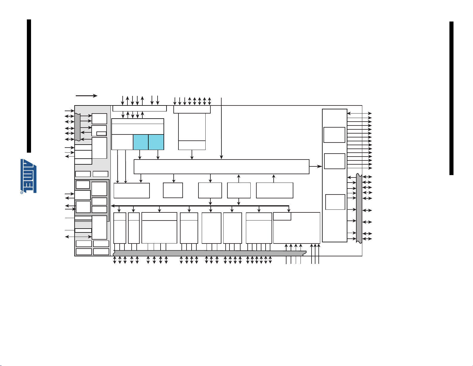
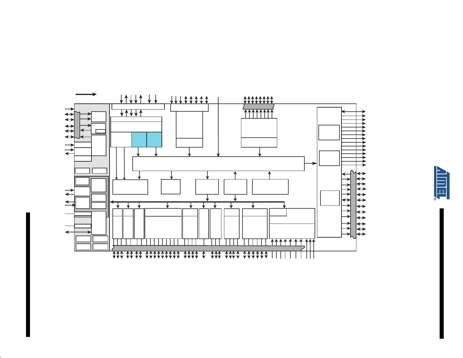
The AT91SAM9R64/RL64 device is based on the integration of an ARM926EJ-S processor with
a large fast SRAM and a wide range of peripherals.
The AT91SAM9R64/RL64 embeds one USB Device High Speed Controller, one LCD Controller
(for AT91SAM9RL64 only), one AC97 controller, a 2-channel DMA Controller, four USARTs, two
SSCs, one SPI, two TWIs, three Timer Counter channels, a 4-channel PWM generator, one Multimedia Card interface and a 6-channel Analog-to-digital converter that also provides touch
screen management.
The AT91SAM9R64/RL64 is architectured on a 6-layer bus matrix. It also features an External
Bus Interface capable of interfacing with a wide range of memory and peripheral devices.
Some features are not available for AT91SAM9R64 in the 144-ball BGA package.
Separate block diagrams and PIO multiplexing are provided in this document. Table 1-1 lists the
features and signals of AT91SAM9RL64 that are not available or partially available for
AT91SAM9R64. When the signal is multiplexed on a PIO, the PIO line is specified.
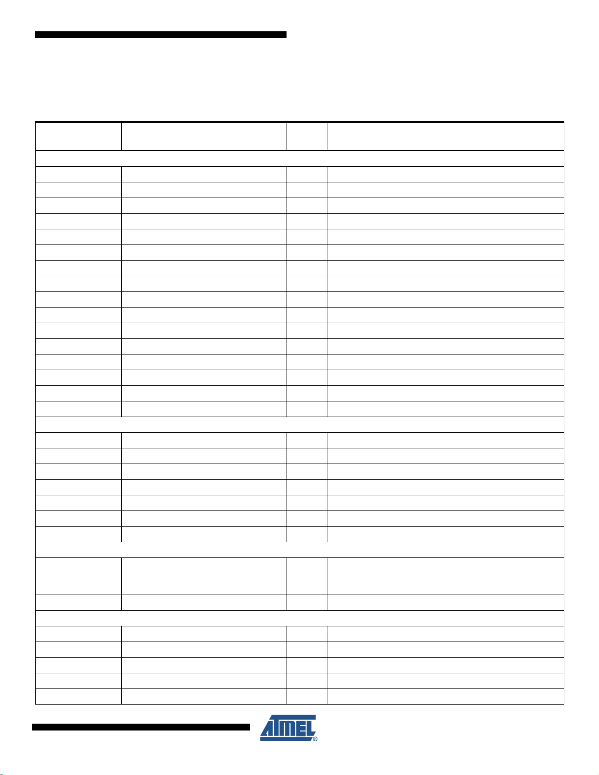
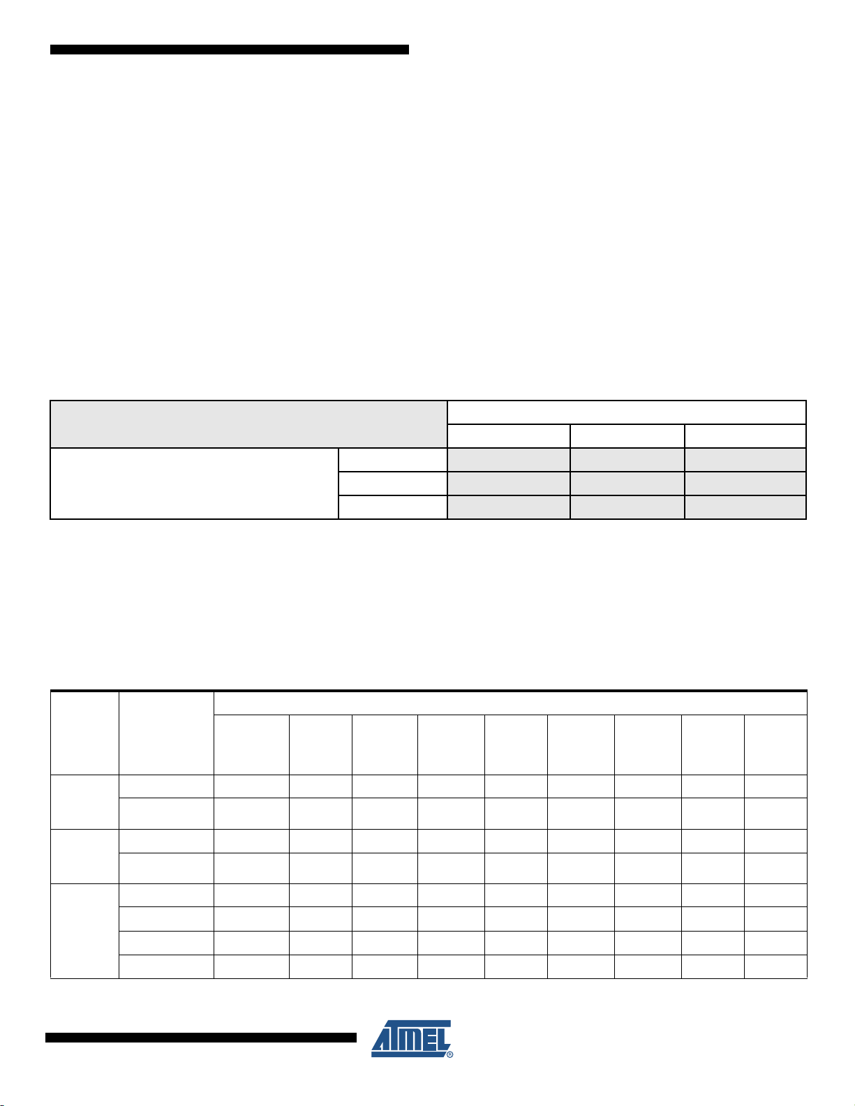
Table 1-1. Unavailable or Partially Available Features and Signals in AT91SAM9R64
Feature Full/Partial Signal Peripheral A Peripheral B
AC97 Full
EBI Partial
AC97FS
AC97CK
AC97TX
AC97RX
D16-D31
NCS2
NCS5/CFCS1
PD1
PD2
PD3
PD4
PB16-PB31
PD0
PD13
-
-
6289BS–ATARM–07-Oct-08
3
Table 1-1. Unavailable or Partially Available Features and Signals in AT91SAM9R64
Feature Full/Partial Signal Peripheral A Peripheral B
LCDMOD
LCDCC
LCDVSYNC
LCDC Full
PWM Partial PWM2 PD5 and PD12 -
SPI Partial
SSC1 Full
LCDHSYNC
LCDDOTCK
LCDDEN
LCDD0-LCDD23
NPCS2
NPCS3
RF1
RK1
TD1
RD1
TK1
TF1
PC2
PC3
PC4
PC5
PC6
PC7
PC8-PC31
PD8
-
-
PD9 and PD13
PA 8
PA 9
PA 1 3
PA 1 4
PA 2 9
PA 3 0
Touchscreen
ADC
TC Partial
TWI Full
USART0 Partial
USART1 Partial SCK1 - PD2
USART2 Partial
Partial
AD3YM
GPAD4
GPAD5
TIOA1
TIOB1
TCLK1
TIOA2
TIOB2
TWD1
TWCK1
SCK0
RTS0
CTS0
DSR0
DTR0
DCD0
RI0
SCK2
RTS2
CTS2
PA 20
PD6
PD7
-
PD10
PD11
PA 8
PA 9
PA 10
PD14
PD15
PD16
PD17
PD9
PA 29
PA 30
-
PC29
PC30
PC31
PD10
PD11
-
-
-
SCK3
USART3 Partial
4
AT91SAM9R64/RL64 Preliminary
RTS3
CTS3
-
PA 2 0
PD3
PD4
6289BS–ATARM–07-Oct-08
6289BS–ATARM–07-Oct-08
AIC
D0-D15
A0/NBS0
A2-A15
A16/BA0
A17/BA1
NCS0
NCS1/SDCS
NRD/CFOE
NWR0/NWE/CFWE
NWR1/NBS1/CFIOR
NWR3/NBS3/CFIOW
SDCK, SDCKE
RAS, CAS
SDWE, SDA10
FIQ
IRQ
PLLRCA
DRXD
DTXD
APB
PLLA
A1/NBS2/NWR2
TST
PCK0-PCK1
System Controller
VDDBU
SHDN
WKUP
XIN
NRST
NANDOE, NANDWE
PMC
UPLL
XOUT
WDT
RTT
32 kHz
OSC
XIN32
XOUT32
SHDC
RSTC
DBGU
SLAVEMASTER
PDC
4
GPBREG
A23-A24, A18-A20
A25/CFRNW
NCS4/CFCS0
NWAIT
CFCE1-CFCE2
EBI
Static
Memory
Controller
CompactFlash
NAND Flash
& ECC
NCS3/NANDCS
TWI0
USART0
USART1
USART2
USART3
PWM
TC0
TC1
TC2
SSC0
PDC
Peripheral
DMA
Controller
Peripheral
Bridge
ROM
32K Bytes
2-channel
DMA
12 MHz
OSC
USB
Device
HS
3-channel 10-bit ADC
PDC
SDRAM
Controller
DA0-DA3
CDA
CK
TWD0
TWCK0
CTS1
RTS1
RXD0-RXD3
TXD0-TXD3
NPCS0-NPCS1
SPCK
MOSI
MISO
TIOA0
TIOB0
TK0
TF0
TD0
RD0
RF0
RK0
TSADTRG
AD0
TSADVREF
VDDANA
GNDAN
SRAM
64K Bytes
HS UTMI
Transceiver
POR
ARM926EJ-S Processor
JTAG Selection and Boundary Scan
In-Circuit Emulator
TDI
TDO
TMS
TCK
JTAGSEL
I
RTCK
ICache
4 Kbytes
DCache
4 Kbytes
BMS
RTC
RC
TCM
Interface
ITCM DTCM
A21/NANDALE
A22/NANDCLE
POR
VDDCORE
AD1
PDC
AD2
5-layer AHB Bus Matrix
D
PIT
PIOA
PIOC
PIOD
PIOB
PDC
PDC
PDC
DMA
VBG
DFSDP
DFSDM
DHSDP
DHSDM
GNDUTMI
VDDUTMII
VDDUTMIC
PWM1
TCLK0
TCLK2
PWM3
PWM0
SPI
MCI
NTRST
Figure 2-1. AT91SAM9R64 Block Diagram
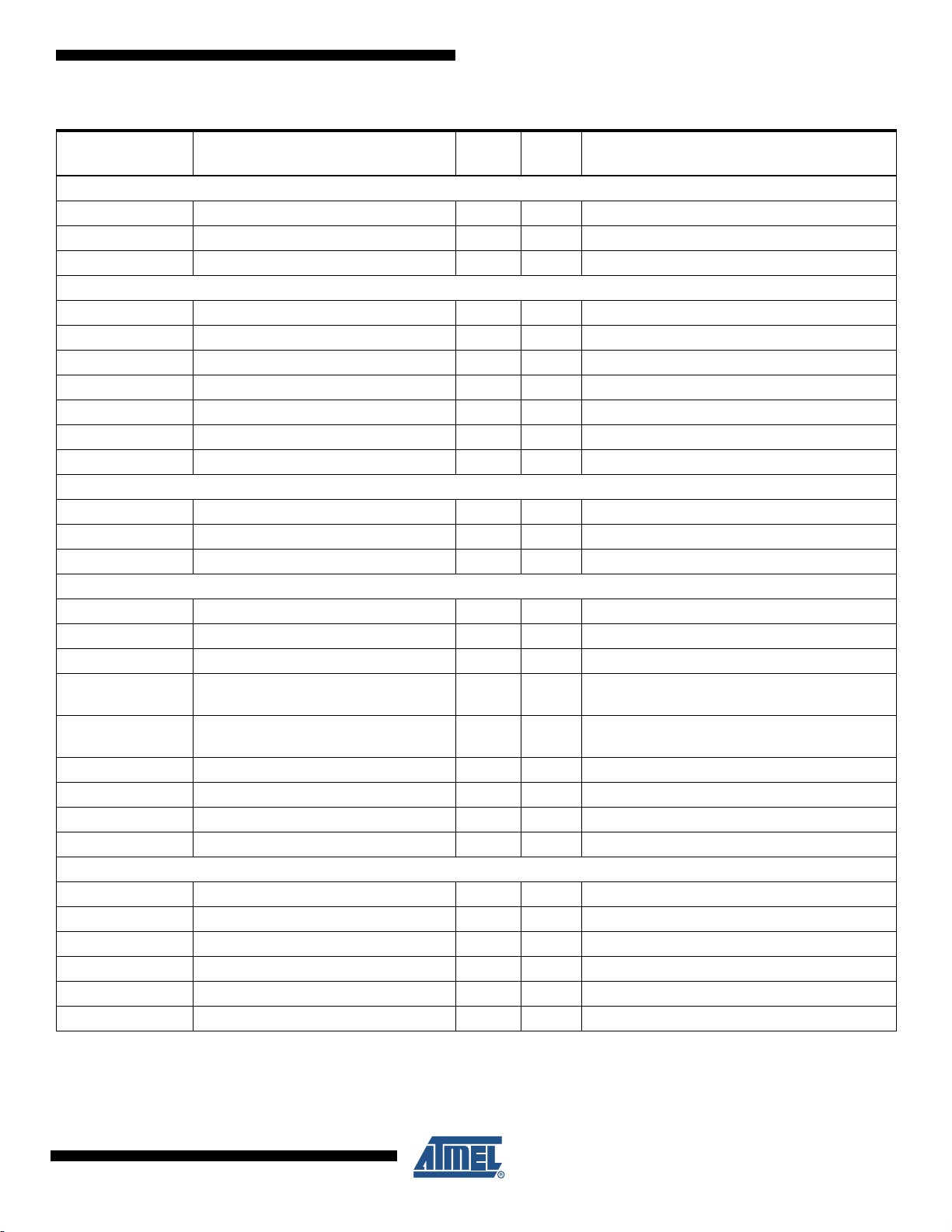
2. Block Diagrams
AT91SAM9R64/RL64 Preliminary
5
6
AIC
D0-D15
A0/NBS0
A2-A15
A16/BA0
A17/BA1
NCS0
NCS1/SDCS
NRD/CFOE
NWR0/NWE/CFWE
NWR1/NBS1/CFIOR
NWR3/NBS3/CFIOW
SDCK, SDCKE
RAS, CAS
SDWE, SDA10
FIQ
IRQ
PLLRCA
DRXD
DTXD
APB
PLLA
A1/NBS2/NWR2
TST
PCK0-PCK1
System Controller
VDDBU
SHDN
WKUP
XIN
NRST
NANDOE, NANDWE
PMC
UPLL
XOUT
WDT
RTT
OSC
32K
XIN32
XOUT32
SHDC
RSTC
DBGU
SLAVEMASTER
PDC
4
GPBREG
A23-A24 A18-A20
NCS5/CFCS1
A25/CFRNW
NCS4/CFCS0
D16-D31
NWAIT
CFCE1-CFCE2
EBI
Static
Memory
Controller
CompactFlash
NAND Flash
& ECC
NCS2
NCS3/NANDCS
MCI
TWI0
USART0
USART1
USART2
USART3
SPI
PWM
TC0
TC1
TC2
AC97
PDC
SSC0
SSC1
PDC
Peripheral
DMA
Controller
Peripheral
Bridge
ROM
32K Bytes
2-channel
DMA
OSC
12M
USB
Device
HS
6-channel 10-bit ADC
PDC
SDRAM
Controller
DA0-DA3
CDA
CK
TWD0
TWCK0
CTS0-CTS3
RTS0-RTS3
SCK0-SCK3
RXD0-RXD3
TXD0-TXD3
NPCS0-NPCS3
SPCK
MOSI
MISO
PWM0-PWM3
TCLK0-TCLK2
TIOA0-TIOA2
TIOB0-TIOB2
AC97CK
AC97FS
AC97RX
AC97TX
TK0-TK1
TF0-TF1
TD0-TD1
RD0-RD1
RF0-RF1
RK0-RK1
TSADTRG
AD0X
P
TSADVREF
VDDANA
GNDAN
VBG
DFSDP
DFSDM
LCDC
SRAM
64K Bytes
HS UTMI
Transceiver
POR
DHSDP
DHSDM
GNDUTMI
VDDUTMII
ARM926EJ-S Processor
JTAG Selection and Boundary Scan
In-Circuit Emulator
TDI
TDO
TMS
TCK
JTAGSEL
I
RTCK
ICache
4 Kbytes
DCache
4 Kbytes
BMS
NTRST
RTC
RC
TCM
Interface
ITCM DTCM
A21/NANDALE
A22/NANDCLE
POR
VDDCORE
AD1X
M
Touch
Screen
Controller
GPAD4
GPAD5
DCD0
DSR0
DTR0
RI0
PDC
AD2Y
P
AD3Y
M
TWI1
TWD1
TWCK1
6-layer AHB Bus Matrix
D
DMA
PIT
PIOA
PIOC
PIOD
PIOB
PDC
PDC
PDC
DMA
VDDUTMIC
LCDD0-LCDD23
LCDVSYNC
LCDHSYNC
LCDDOTCK
LDDEN
LCDCC
LCDPWR
LCDMOD
AT91SAM9R64/RL64 Preliminary
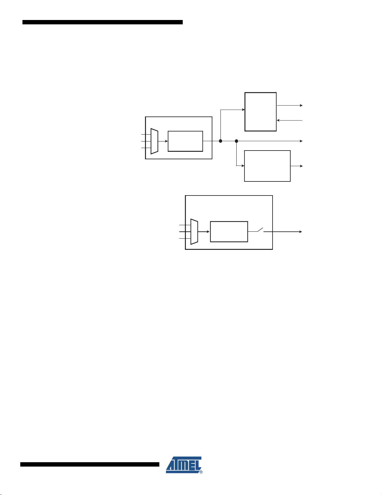
Figure 2-2. AT91SAM9RL64 Block Diagram
6289BS–ATARM–07-Oct-08
AT91SAM9R64/RL64 Preliminary
3. Signal Description
Table 3-1 gives details on the signal name classified by peripheral.
Table 3-1. Signal Description List
Active
Signal Name Function Type
Power Supplies
VDDIOM EBI I/O Lines Power Supply Power 1.65V to 3.6V
VDDIOP Peripherals I/O Lines Power Supply Power 3.0V to 3.6V
VDDUTMII USB UTMI+ Interface Power Supply Power 3.0V to 3.6V
VDDUTMIC USB UTMI+ Core Power Supply Power 1.08V to 1.32V
GNDUTMI USB UTMI Ground Ground
VDDBU Backup I/O Lines Power Supply Power 1.08V to 1.32V
GNDBU Backup Ground Ground
VDDPLLA PLL Power Supply Power 3.0V to 3.6V
GNDPLLA PLL Ground Ground
VDDPLLB UTMI PLL and OSC 12M Power Supply Power 1.08 V to 1.32V
GNDPLLB UTMI PLL and OSC 12M Ground Ground
VDDANA ADC Analog Power Supply Power 3.0V to 3.6V
GNDANA ADC Analog Ground Ground
VDDCORE Core Chip Power Supply Power 1.08V to 1.32V
GNDCORE Ground Ground
GND Ground Ground
Clocks, Oscillators and PLLs
XIN Main Oscillator Input Input
XOUT Main Oscillator Output Output
XIN32 Slow Clock Oscillator Input Input
XOUT32 Slow Clock Oscillator Output Output
VBG Bias Voltage Reference Analog
PLLRCA PLL A Filter Input
PCK0 - PCK1 Programmable Clock Output Output
Shutdown, Wakeup Logic
SHDN Shutdown Control Output
WKUP Wake-Up Input Input Accept between 0V and VDDBU
ICE and JTAG
TCK Test Clock Input No pull-up resistor
TDI Test Data In Input No pull-up resistor
TDO Test Data Out Output
TMS Test Mode Select Input No pull-up resistor
JTAGSEL JTAG Selection Input Pull-down resistor
Level Comments
Driven at 0V only.
0: The device is in backup mode.
1: The device is running (not in backup mode.)
6289BS–ATARM–07-Oct-08
7
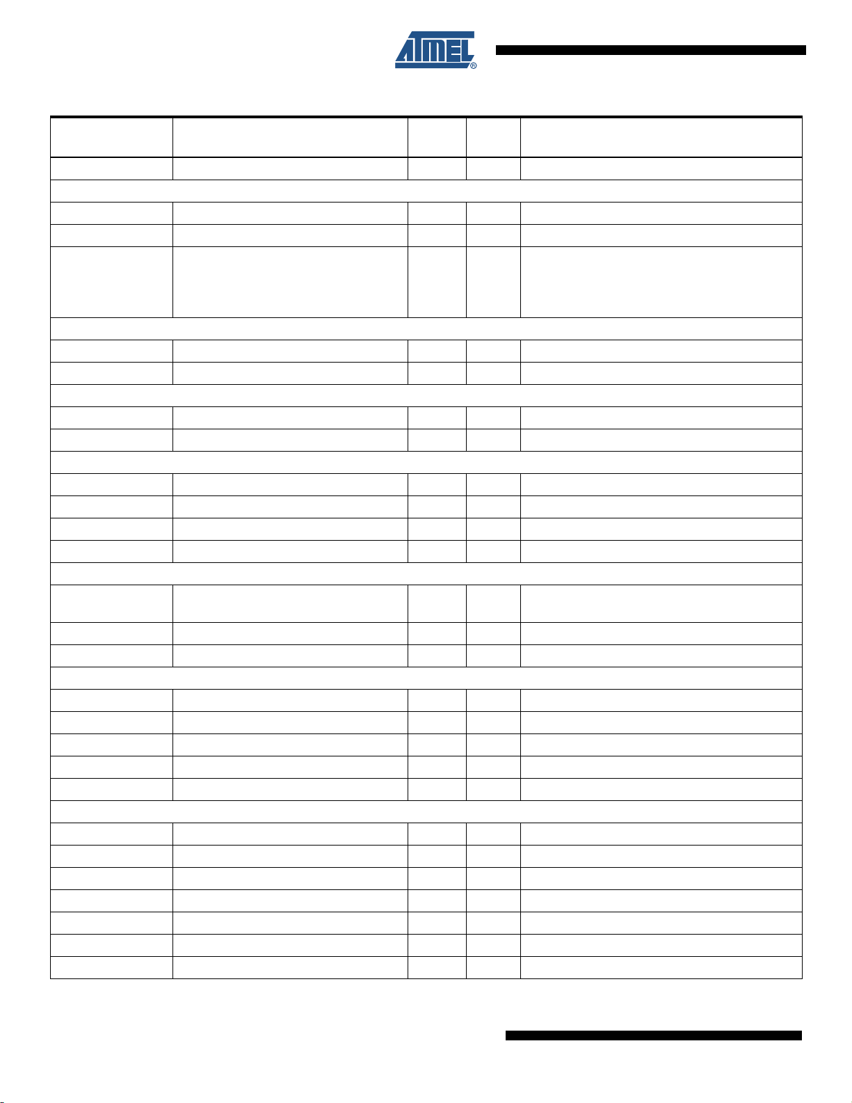
Table 3-1. Signal Description List (Continued)
Active
Signal Name Function Type
NTRST Test Reset Signal Input Low Pull-up resistor.
Reset/Test
NRST Microcontroller Reset I/O Low Pull-up resistor
TST Test Mode Select Input Pull-down resistor
BMS Boot Mode Select Input
Debug Unit - DBGU
DRXD Debug Receive Data Input
DTXD Debug Transmit Data Output
Advanced Interrupt Controller - AIC
IRQ External Interrupt Input Input
FIQ Fast Interrupt Input Input
PIO Controller - PIOA - PIOB - PIOC-PIOD
PA0 - PA31 Parallel IO Controller A I/O Pulled-up input at reset
PB0 - PB31 Parallel IO Controller B I/O Pulled-up input at reset
PC0 - PC31 Parallel IO Controller C I/O Pulled-up input at reset
PD0 - PD21 Parallel IO Controller D I/O Pulled-up input at reset
External Bus Interface - EBI
D0 - D31 Data Bus I/O
A0 - A25 Address Bus Output 0 at reset
NWAIT External Wait Signal Input Low
Static Memory Controller - SMC
NCS0 - NCS5 Chip Select Lines Output Low NCS2, NCS5 not present on AT91SAM9R64.
NWR0 - NWR3 Write Signal Output Low
NRD Read Signal Output Low
NWE Write Enable Output Low
NBS0 - NBS3 Byte Mask Signal Output Low
CompactFlash Support
CFCE1 - CFCE2 CompactFlash Chip Enable Output Low
CFOE CompactFlash Output Enable Output Low
CFWE CompactFlash Write Enable Output Low
CFIOR CompactFlash IO Read Output Low
CFIOW CompactFlash IO Write Output Low
CFRNW CompactFlash Read Not Write Output
CFCS0 - CFCS1 CompactFlash Chip Select Lines Output Low CFCS1 not present on AT91SAM9R64.
Level Comments
Must be connected to GND or VDDIOP.
No pullup resistor
BMS = 0 when tied to GND
BMS = 1 when tied to VDDIOP
Pulled-up input at reset. D16-D31 not present
on AT91SAM9R64.
8
AT91SAM9R64/RL64 Preliminary
6289BS–ATARM–07-Oct-08
AT91SAM9R64/RL64 Preliminary
Table 3-1. Signal Description List (Continued)
Active
Signal Name Function Type
NAND Flash Support
NANDCS NAND Flash Chip Select Output Low
NANDOE NAND Flash Output Enable Output Low
NANDWE NAND Flash Write Enable Output Low
SDRAM Controller
SDCK SDRAM Clock Output
SDCKE SDRAM Clock Enable Output High
SDCS SDRAM Controller Chip Select Output Low
BA0 - BA1 Bank Select Output
SDWE SDRAM Write Enable Output Low
RAS - CAS Row and Column Signal Output Low
SDA10 SDRAM Address 10 Line Output
Multimedia Card Interface MCI
CK Multimedia Card Clock I/O
CDA Multimedia Card Slot A Command I/O
DA0 - DA3 Multimedia Card Slot A Data I/O
Universal Synchronous Asynchronous Receiver Transmitter USARTx
SCKx USARTx Serial Clock I/O SCKx not present on AT91SAM9R64.
TXDx USARTx Transmit Data I/O
RXDx USARTx Receive Data Input
RTSx USARTx Request To Send Output
CTSx USARTx Clear To Send Input
DTR0 USART0 Data Terminal Ready I/O Not present on AT91SAM9R64.
DSR0 USART0 Data Set Ready Input Not present on AT91SAM9R64.
DCD0 USART0 Data Carrier Detect Output Not present on AT91SAM9R64.
RI0 USART0 Ring Indicator Input Not present on AT91SAM9R64.
Synchronous Serial Controller - SSCx
TD0 - TD1 SSC Transmit Data Output TD1 not present on AT91SAM9R64.
RD0 - RD1 SSC Receive Data Input RD1 not present on AT91SAM9R64.
TK0 - TK1 SSC Transmit Clock I/O TK1 not present on AT91SAM9R64.
RK0 - RK1 SSC Receive Clock I/O RK1 not present on AT91SAM9R64.
TF0 - TF1 SSC Transmit Frame Sync I/O TF1 not present on AT91SAM9R64.
RF0 - RF1 SSC Receive Frame Sync I/O RF1 not present on AT91SAM9R64.
Level Comments
RTS0, RTS2, RTS3 not present on
AT91SAM9R64.
CTS0, CTS2, CTS3 not present on
AT91SAM9R64.
6289BS–ATARM–07-Oct-08
9

Table 3-1. Signal Description List (Continued)
Active
Signal Name Function Type
AC97 Controller - AC97C
AC97RX AC97 Receive Signal Input Not present on AT91SAM9R64.
AC97TX AC97 Transmit Signal Output Not present on AT91SAM9R64.
AC97FS AC97 Frame Synchronization Signal Output Not present on AT91SAM9R64.
AC97CK AC97 Clock signal Input Not present on AT91SAM9R64.
Timer/Counter - TC
TCLKx TC Channel x External Clock Input Input TCLK1 not present on AT91SAM9R64.
TIOAx TC Channel x I/O Line A I/O TIOA1, TIOA2 not present on AT91SAM9R64.
TIOBx TC Channel x I/O Line B I/O TIOB1, TIOB2 not present on AT91SAM9R64.
Pulse Width Modulation Controller- PWMC
PMWx Pulse Width Modulation Output Output PWM2 not present on AT91SAM9R64.
Serial Peripheral Interface - SPI
MISO Master In Slave Out I/O
MOSI Master Out Slave In I/O
SPCK SPI Serial Clock I/O
NPCS0 SPI Peripheral Chip Select 0 I/O Low
NPCS1 - NPCS3 SPI Peripheral Chip Select Output Low NPCS2, NPCS3 not present on AT91SAM9R64.
Two-Wire Interface - TWIx
TWDx TWIx Two-wire Serial Data I/O TWD1 not present on AT91SAM9R64.
TWCKx TWIx Two-wire Serial Clock I/O TWCK1 not present on AT91SAM9R64.
Touch Screen Analog-to-Digital Converter
GPAD0-GPAD5 Analog Inputs Analog GPAD4, GPAD5 not present on AT91SAM9R64.
AD0X
AD1X
AD2Y
AD3Y
P
M
P
M
Touch Panel Right side Analog Multiplexed with AD0
Touch Panel Left side Analog Multiplexed with AD1
Touch Panel Top side Analog Multiplexed with AD2
Touch Panel Bottom side Analog
TSADTRG ADC Trigger Input
TSADVREF ADC Reference Analog
LCD Controller - LCDC
LCDD0 - LCDD23 LCD Data Bus Output Not present on AT91SAM9R64.
LCDVSYNC LCD Vertical Synchronization Output Not present on AT91SAM9R64.
LCDHSYNC LCD Horizontal Synchronization Output Not present on AT91SAM9R64.
LCDDOTCK LCD Dot Clock Output Not present on AT91SAM9R64.
LCDDEN LCD Data Enable Output Not present on AT91SAM9R64.
LCDCC LCD Contrast Control Output Not present on AT91SAM9R64.
LCDPWR LCD panel Power enable control Output Not present on AT91SAM9R64.
LCDMOD LCD Modulation signal Output Not present on AT91SAM9R64.
Level Comments
Multiplexed with AD3. Not present on
AT91SAM9R64.
10
AT91SAM9R64/RL64 Preliminary
6289BS–ATARM–07-Oct-08
AT91SAM9R64/RL64 Preliminary
Table 3-1. Signal Description List (Continued)
Signal Name Function Type
USB High Speed Device
DFSDM USB Device Full Speed Data - Analog
DFSDP USB Device Full Speed Data + Analog
DHSDM USB Device High Speed Data - Analog
DHSDP USB Device High Speed Data + Analog
Active
Level Comments
6289BS–ATARM–07-Oct-08
11
4. Package and Pinout
BALL A1
12
1
2
3
4
5
6
7
8
9
10
11
ABCDE F GHJ KL M
The AT91SAM9R64 is available in a 144-ball BGA package. The AT91SAM9RL64 is available
in a 217-ball LFBGA package.
4.1 144-ball BGA Package Outline
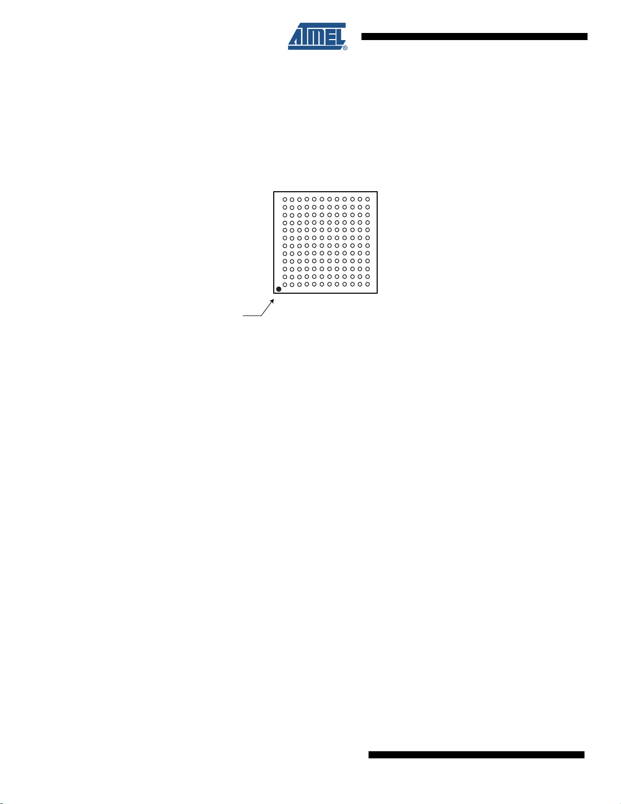
Figure 4-1 shows the orientation of the 144-ball BGA package.
Figure 4-1. 144-ball BGA Pinout (Top View)
12
AT91SAM9R64/RL64 Preliminary
6289BS–ATARM–07-Oct-08
AT91SAM9R64/RL64 Preliminary
4.2 Pinout
AT91SAM9R64 Pinout for 144-ball BGA Package
Pin Signal Name Pin Signal Name Pin Signal Name Pin Signal Name
A1 DFSDM D1 PLLRCA G1 PB[10] K1 A[5]
A2 DHSDM D2 VDDUTMII
A3 XIN
A4 XOUT
A5 XIN32 D5 JTAGSEL
A6 XOUT32 D6 GNDBU G6 GND
A7 TDO D7 TCK G7 GND
A8 PA[31] D8 PA[26] G8 GND
A9 PA[22] D9 PA[24] G9 GNDUTMI
A10 PA[16] D10 PA[13] G10 VDDCORE
A11 PA[14] D11 PA[6] G11 VDDIOP
A12 PA[11] D12 PD[20] G12 VDDIOP K12 PB[1]
B1 DFSDP E1 GNDPLLA
B2 DHSDP
B3 NC
B4 VDDPLLB
B5 GNDPLLB
B6 TMS
B7 RTCK E7 NRST H7 GND
B8 PA[27] E8 BMS H8 GND
B9 PA[21] E9 PA[25]
B10 PA[12] E10 PA[15]
B11 PD[21] E11 PA[5] H11 VDDCORE L11 PB[0]
B12 PA[10] E12 PA[4] H12 VDDIOP L12 GNDANA
C1 VDDPLLA
C2 VBG
C3 VDDBU
C4 SHDN
C5 WKUP
C6 NTRST
C7 TDI F7 TST
C8 PA[28] F8 VDDUTMIC
C 9 PA [ 2 3] F9 PA [ 3]
C10 PA[7] F10 PA[2]
C11 PD[19] F11 PA[0]
C12 PD[18] F12 PA[1]
D3 NWR3/NBS3/CFIOW G3 PB[12] K3 A[13]
D4 NWR1/NBS1/CFIOR G4 PB[9] K4 A[15]
E2 NWR0/NWE/CFWE H2 PB[15] L2 A[8]
E3 NRD/CFOE H3 A[0] L3 A[11]
E4 NCS0 H4 A[2] L4 A[16]
E5 NCS1/SDCS H5 SDA10 L5 SDWE
E6 PB[2] H6 D[1] L6 D[4]
F1 PB[5] J1 A[4] M1 A[9]
F2 PB[6] J2 A[1] M2 A[10]
F3 PB[7] J3 A[3] M3 A[12]
F4 PB[8] J4 A[14] M4 A[17]
F5 PB[3] J5 CAS M5 D[0]
F6 PB[4] J6 D[2] M6 SDCK
G2 PB[11] K2 A[6]
G5 PB[13] K5 RAS
K6 D[3]
K7 D[6]
K8 D[13]
K9 VDDIOM
K10 VDDIOM
K11 D[11]
H1 PB[14] L1 A[7]
L7 D[7]
L8 D[15]
H9 VDDIOM L9 PC[1]
H10 SDCKE L10 PC[0]
J7 D[5] M7 D[8]
J8 D[12] M8 ADVREF
J9 D[14] M9 VDDANA
J10 VDDIOM M10 PA[17]
J11 D[10] M11 PA[18]
J12 D[9] M12 PA[19]
4.3 217-ball LFBGA Package Outline
Figure 4-2 shows the orientation of the 217-ball LFBGA package.
6289BS–ATARM–07-Oct-08
13
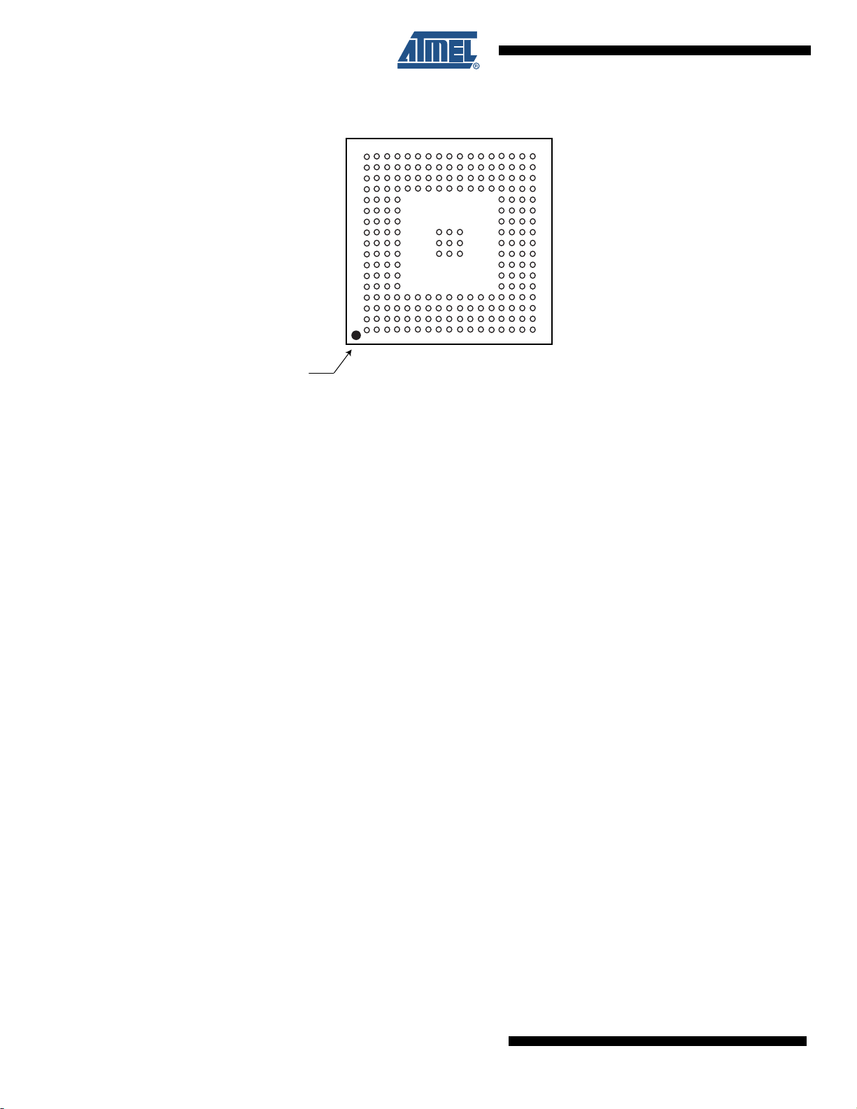
Figure 4-2. 217-ball LFBGA Pinout (Top View)
BALL A1
12
1
2
3
4
5
6
7
8
9
10
11
13
14
15
16
17
ABCDEFGHJ KLM NPRTU
14
AT91SAM9R64/RL64 Preliminary
6289BS–ATARM–07-Oct-08
AT91SAM9R64/RL64 Preliminary
4.4 Pinout
Table 4-1. AT91SAM9RL64 Pinout for 217-ball LFBGA Package
Pin Signal Name Pin Signal Name Pin Signal Name Pin Signal Name
A1 DFSDM D5 SHDN J14 PD[1] P17 PC[11]
A2 DHSDP D6 JTAGSEL J15 PD[0] R1 A[0]
A3 VDDPLLB D7 NTRST J16 PC[30] R2 A[2]
A4 XIN D8 BMS J17 PC[31] R3 A[7]
A5 XOUT D9 TDO K1 PB[14] R4 A[10]
A6 GNDPLLB D10 PA [ 3 0] K2 PB[15] R5 A[14]
A7 XOUT32 D11 GND K3 PB[17] R6 SDA10
A8 GND D12 PA [ 2 3 ] K4 PB[16] R7 D[0]
A9 NRST D13 PA [ 15 ] K8 VDDUTMIC R8 VDDIOM
A10 RTCK D14 PA[ 1 2 ] K9 VDDIOP R9 D[6]
A11 PA[29] D15 PA [ 8 ] K10 PC[28] R10 D[9]
A12 PA[26] D16 PD[13] K14 PC[25] R11 NC
A13 PA[22] D17 PD[16] K15 PC[24] R12 VDDIOM
A14 PA[14] E1 GNDPLLA K16 PC[26] R13 PC[1]
A15 PA[10] E2 NCS1/SDCS K17 PC[27] R14 PB[1]
A16 PD[20] E3 NCS0 L1 PB[18] R15 PC[5]
A17 PD[17] E4 NWR3/NBS3/CFIOW L2 PB[19] R16 PC[6]
B1 DFSDP E14 PD[15] L3 PB[21] R17 PC[7]
B2 DHSDM E15 PD[14] L4 PB[20] T1 A[3]
B3 VBG E16 PA[ 5 ] L14 PC[21] T2 A[5]
B4 NC E17 PA [4 ] L15 PC[20] T3 A[8]
B5 NC F1 NRD/CFOE L16 PC[22] T4 A[12]
B6 XIN32 F2 PB[2] L17 PC[23] T5 A[16]
B7 TST F3 NWR0/NWE/CFWE M1 PB[22] T6 RAS
B8 GND F4 PB[3] M2 PB[23] T7 D[2]
B9 TMS F14 PA [ 1] M3 PB[25] T8 D[4]
B10 VDDCORE F15 PA [0 ] M4 PB[24] T9 D[7]
B11 PA[28] F16 PA [ 2 ] M14 PC[17] T10 D[10]
B12 PA[25] F17 PA [ 3 ] M15 PC[16] T11 D[14]
B13 PA[21] G1 GND M16 PC[18] T12 VDDANA
B14 PA[13] G2 VDDIOM M17 PC[19] T13 PA [1 7 ]
B15 PD[21] G3 PB[5] N1 PB[26] T14 PA [ 19 ]
B16 PD[19] G4 PB[4] N2 PB[27] T15 PC[2]
B17 PA [ 9] G14 PD[12] N3 PB[29] T16 PC[3]
C1 VDDPLLA G15 PD[11] N4 PB[28] T17 PC[4]
C2 VDDUTMII G16 PD[10] N14 PC[13] U1 A[4]
C3 GND G17 PD[9] N15 PC[12] U2 A[6]
C4 GNDUTMI H1 PB[8] N16 PC[14] U3 A[9]
C5 VDDBU H2 PB[9] N17 PC[15] U4 A[13]
C6 WKUP H3 PB[7] P1 PB[30] U5 A[17]
C7 GNDBU H4 PB[6] P2 PB[31] U6 SDWE
C8 TCK H8 VDDCORE P3 A[1] U7 D[3]
C9 TDI H9 VDDIOP P4 A[11] U8 SDCK
C10 PA[31] H10 PD[4] P5 A[15] U9 D[11]
C11 PA[27] H14 PD[8] P6 CAS U10 D[12]
C12 PA[24] H15 PD[5] P7 D[1] U11 D[13]
C13 PA[16] H16 PD[2] P8 SDCKE U12 TSADVREF
C14 PA[11] H17 PD[3] P9 D[5] U13 PA [ 1 8]
C15 PD[18] J1 PB[12] P10 D[8] U14 PA [ 2 0 ]
C16 PA[ 7 ] J2 PB[13] P11 D[15] U15 PD[6]
C17 PA[ 6 ] J3 PB[11] P12 PC[0] U16 PD[7]
D1 PLLRCA J4 PB[10] P13 PB[0] U17 GNDANA
D2 NWR1/NBS1/CFIOR J8 VDDCORE P14 PC[8]
D3 GND J9 VDDIOP P15 PC[9]
D4 GND J10 PC[29] P16 PC[10]
(1)
Note: 1. Shaded cells define the pins powered by VDDIOM.
6289BS–ATARM–07-Oct-08
15

5. Power Considerations
5.1 Power Supplies
The AT91SAM9R64/RL64 has several types of power supply pins:
• VDDCORE pins: Power the core, including the processor, the embedded memories and the
peripherals; voltage ranges from 1.08V and 1.32V, 1.2V nominal.
• VDDIOM pins: Power the External Bus Interface; voltage ranges between 1.65V and 1.95V
(1.8V nominal) or between 3.0V and 3.6V (3.3V nominal).
• VDDIOP pins: Power the Peripherals I/O lines; voltage ranges from 3.0V and 3.6V, 3.3V
nominal.
• VDDBU pin: Powers the Slow Clock oscillator and a part of the System Controller; voltage
ranges from 1.08V and 1.32V, 1.2V nominal.
• VDDPLLA pin: Powers the PLL cell; voltage ranges from 3.0V and 3.6V, 3.3V nominal.
• VDDPLLB pin: Powers the UTMI PLL (480MHz) and OSC 12M cells; voltage ranges from
1.08V and 1.32V, 1.2V nominal.
• VDDUTMII pin: Powers the UTMI+ interface; voltage ranges from 3.0V and 3.6V, 3.3V
nominal.
• VDDUTMIC pin: Powers the UTMI+ core; voltage ranges from 1.08V and 1.32V, 1.2V
nominal.
• VDDANA pin: Powers the ADC cell; voltage ranges from 3.0V and 3.6V, 3.3V nominal.
The power supplies VDDIOM and VDDIOP are identified in the pinout table and the PIO multiplexing tables. These supplies enable the user to power the device differently for interfacing with
memories and for interfacing with peripherals.
5.1.1 USB
Ground pins GND are common to VDDCORE, VDDIOM and VDDIOP pins power supplies.
Separated ground pins are provided for VDDBU, VDDPLLA, VDDPLLB and VDDANA. These
ground pins are respectively GNDBU, GNDPLLA, GNDPLLB and GNDANA. A common ground
pin is provided for VDDUTMII and VDDUTMIC. This ground pin is GNDUTMI.
Caution: VDDCORE and VDDIO constraints at startup to be checked in the Core Power Supply
POR Characteristics in the Electical Characteristics section of the datasheet.
Power Supply Considerations
To achieve the best performances on the UDPHS, care must be taken in the power supplies
choice and especially on VDDPLLB,VDDUTMIC and VDDUTMII.
The USB High speed requires power supplies with a ripple voltage < 20 mV on VDDPLLB and
VDDUTMIC. The VDDUTMII powering the UTMI transceiver must also be filtered.
It is highly recommended to use an LDO linear regulator to generate the 1.2 volts for both
VDDPLLB and VDDUTMIC. VDDUTMII can be connected on the 3.3 volts of the system via an
LC filter.
The figure below gives an example of VDDPLLB, VDDUTMIC and VDDUTMII.
16
AT91SAM9R64/RL64 Preliminary
6289BS–ATARM–07-Oct-08
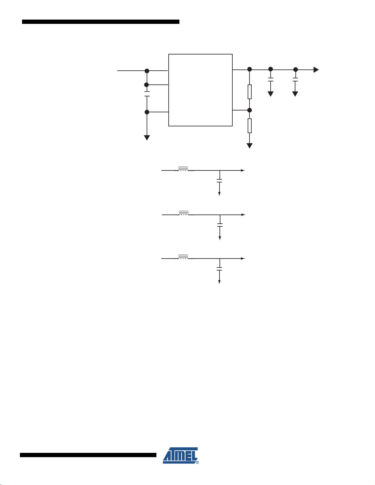
AT91SAM9R64/RL64 Preliminary
VIN
CE
VSS
VOUT
ADJ
10µF 0.1µF
10µF
MIC5235YM5
1K
100K
VIN
1V2_USB
0.1µF
1V2_USB
2.2µH
VDDPLLB
0.1µF
1V2_USB
2.2µH
VDDUTMIC
0.1µF
3V3
2.2µH
VDDUTMII
Figure 5-1. Example of PLL and USB Power Supplies
5.2 Power Consumption
The AT91SAM9R64/RL64 consumes about 450 µA of static current on VDDCORE at 25°C and
up to 4 mA at 85°C.
On VDDBU, the current does not exceed 5 µA @25°C and 30 µA @85°C.
For dynamic power consumption, the AT91SAM9R64/RL64 consumes a maximum of 70 mA on
VDDCORE in worst case conditions (1.2V, 85°C, processor running full-performance algorithm).
5.3 Programmable I/O Lines Power Supplies
The power supplies pins VDDIOM support two voltage ranges. This allows the device to reach
its maximum speed either out of 1.8V or 3.3V external memories.
The maximum speed is MCK on the pin SDCK (SDRAM Clock) loaded with 30pF for power supply at 1.8V and 50 pF for power supply at 3.3V.
The maximum speed on the other signals of the External Bus Interface (control, address and
data signals) is 50 MHz.
6289BS–ATARM–07-Oct-08
17

The voltage ranges are determined by programming registers in the Chip Configuration registers
located in the Matrix User Interface.
At reset, the selected voltage defaults to 3.3V nominal and power supply pins can accept either
1.8V or 3.3V. The user must make sure to program the EBI voltage range before getting the
device out of its Slow Clock Mode.
The PIO lines are supplied through VDDIOP and the speed of the signal that can be driven on
them can reach 50 MHz with 50 pF load.
6. I/O Line Considerations
6.1 JTAG Port Pins
TMS, TDI and TCK are schmitt trigger inputs and have no pull-up resistors.
TDO is an output, driven at up to VDDIOP, and have no pull-up resistor.
The JTAGSEL pin is used to select the JTAG boundary scan when asserted at a high level. It
integrates a permanent pull-down resistor of about 15 kΩ to GNDBU, so that it can be left unconnected for normal operations.
All the JTAG signals are supplied with VDDIOP except JTAGSEL supplied by VDDBU.
6.2 Test Pin
The TST pin is used for manufacturing test purposes when asserted high. It integrates a permanent pull-down resistor of about 15 kΩ to GNDBU, so that it can be left unconnected for normal
operations. Driving this line at a high level leads to unpredictable results.
6.3 Reset Pins
6.4 PIO Controllers
This pin is supplied with VDDBU.
NRST is an open-drain output integrating a non-programmable pull-up resistor. It can be driven
with voltage at up to VDDIOP.
As the product integrates power-on reset cells, which manages the processor and the JTAG
reset, the NRST and NTRST pin can be left unconnected.
The NRST and NTRST pins integrates a permanent pull-up resistor of 100 kΩ typical to
VDDIOP.
The NRST signal is inserted in the Boundary Scan.
All the I/O lines which are managed by the PIO Controllers integrate a programmable pull-up
resistor. Refer to the section “AT91SAM9R64/RL64 Electrical Characteristics” in the product
datasheet for more details.
After reset, all the I/O lines default as inputs with pull-up resistors enabled, except those which
are multiplexed with the External Bus Interface signals that require to be enabled as Peripheral
at reset. This is explicitly indicated in the column “Reset State” of the PIO Controller multiplexing
tables.
18
AT91SAM9R64/RL64 Preliminary
6289BS–ATARM–07-Oct-08

6.5 Shutdown Logic Pins
The SHDN pin is an output only, which is driven by the Shutdown Controller only at low level. It
can be tied high with an external pull-up resistor at VDDBU only.
The pin WKUP is an input-only. It can accept voltages only between 0V and VDDBU.
7. Processor and Architecture
7.1 ARM926EJ-S Processor
• RISC Processor Based on ARM v5TEJ Architecture with Jazelle technology for Java
acceleration
• Two Instruction Sets
– ARM High-performance 32-bit Instruction Set
– Thumb High Code Density 16-bit Instruction Set
• DSP Instruction Extensions
• 5-Stage Pipeline Architecture:
– Instruction Fetch (F)
– Instruction
– Execute (E)
– Data Memory (M)
– Register Write (W)
• 4-Kbyte Data Cache, 4-Kbyte Instruction Cache
– Virtually-addressed 4-way Associative Cache
– Eight words per line
– Write-through and Write-back Operation
– Pseudo-random or Round-robin Replacement
• Write Buffer
– Main Write Buffer with 16-word Data Buffer and 4-address Buffer
– DCache Write-back Buffer with 8-word Entries and a Single Address Entry
– Software Control Drain
• Standard ARM v4 and v5 Memory Management Unit (MMU)
– Access Permission for Sections
– Access Permission for large pages and small pages can be specified separately for
each quarter of the page
– 16 embedded domains
• Bus Interface Unit (BIU)
– Arbitrates and Schedules AHB Requests
– Separate Masters for both instruction and data access providing complete Matrix
system flexibility
– Separate Address and Data Buses for both the 32-bit instruction interface and the
32-bit data interface
– On Address and Data Buses, data can be 8-bit (Bytes), 16-bit (Half-words) or 32-bit
(Words)
Decode (D)
AT91SAM9R64/RL64 Preliminary
6289BS–ATARM–07-Oct-08
19
7.2 Matrix Masters
7.3 Matrix Slaves
The Bus Matrix of the AT91SAM9R64/RL64 product manages 6 masters, which means that
each master can perform an access concurrently with others, to an available slave.
Each master has its own decoder, which is defined specifically for each master. In order to simplify the addressing, all the masters have the same decodings.
Table 7-1. List of Bus Matrix Masters
Master 0 DMA Controller
Master 1 USB Device High Speed DMA
Master 2 LCD Controller DMA
Master 3 Peripheral DMA Controller
Master 4 ARM926™ Instruction
Master 5 ARM926 Data
The Bus Matrix of the AT91SAM9R64/RL64 product manages 6 slaves. Each slave has its own
arbiter, allowing a different arbitration per slave.
Table 7-2. List of Bus Matrix Slaves
Slave 0 Internal ROM
Slave 1 Internal SRAM
Slave 2 LCD Controller User Interface
Slave 3 UDP High Speed RAM
Slave 4 External Bus Interface (EBI)
Slave 5 Peripheral Bridge
7.4 Master to Slave Access
All the Masters can normally access all the Slaves. However, some paths do not make sense,
for example allowing access from the USB Device High speed DMA to the Internal Peripherals.
Thus, these paths are forbidden or simply not wired, and shown as “-” in the following table.
Table 7-3. AT91SAM9R64/RL64 Master to Slave Access
Masters 0 1 2 3 4 5
Slaves
0 Internal ROM X X X X X
1 Internal SRAM X X X X X X
2 LCD Controller User Interface - - - - X X
3 UDP High Speed RAM - - - - X X
4 External Bus Interface X X X X X X
DMA
Controller
USB HS
Device DMA
LCD
Controller
DMA
Peripheral
DMA
ARM926
Instruction
ARM926
Data
5 Peripheral Bridge X X X - - -
20
AT91SAM9R64/RL64 Preliminary
6289BS–ATARM–07-Oct-08

7.5 Peripheral DMA Controller (PDC)
• Acting as one AHB Bus Matrix Master
• Allows data transfers from/to peripheral to/from any memory space without any intervention
of the processor.
• Next Pointer support, prevents strong real-time constraints on buffer management.
The Peripheral DMA Controller handles transfer requests from the channel according to the following priorities (Low to High priorities):
a. TWI0 Transmit Channel
b. DBGU Transmit Channel
c. USART3 Transmit Channel
d. USART2 Transmit Channel
e. USART1 Transmit Channel
f. USART0 Transmit Channel
g. AC97 Transmit Channel
h. SPI Transmit Channel
i. SSC1 Transmit Channel
j. SSC0 Transmit Channel
k. TWI0 Receive Channel
l. DBGU Receive Channel
m. ADC Receive Channel
n. USART3 Receive Channel
o. USART2 Receive Channel
p. USART1 Receive Channel
q. USART0 Receive Channel
r. AC97 Receive Channel
s. SPI Receive Channel
t. SSC1 Receive Channel
u. SSC0 Transmit Channel
v. MCI Receive/Transmit Channel
AT91SAM9R64/RL64 Preliminary
7.6 DMA Controller
• Acting as one Matrix Master
• Embeds 2 channels
• 16 bytes/FIFO for Channel Buffering
• Linked List support with Status Write Back operation at End of Transfer
• Word, Half-word, Byte transfer support
7.7 Debug and Test Features
• ARM926 Real-time In-circuit Emulator
– Two real-time Watchpoint Units
– Two Independent Registers: Debug Control Register and Debug Status Register
– Test Access Port Accessible through JTAG Protocol
6289BS–ATARM–07-Oct-08
21

– Debug Communications Channel
• Debug Unit
–Two-pin UART
– Debug Communication Channel Interrupt Handling
– Chip ID Register
• IEEE1149.1 JTAG Boundary-scan on All Digital Pins
22
AT91SAM9R64/RL64 Preliminary
6289BS–ATARM–07-Oct-08
8. Memories
16K Bytes
0xFFFC 0000
16K Bytes
0xFFFC 4000
0xFFFC C000
SPI
16K Bytes
0xFFFC 8000
16K Bytes
16K Bytes
16K Bytes
0xFFFA 4000
TCO, TC1, TC2
0xFFFA 8000
MCI
0xFFFB 0000
0xFFFB 4000
USART0
0xFFFB C000
USART1
0xFFFA 0000
0xFFFA C000
TWI1
16K Bytes
TWI0
16K Bytes
16K Bytes
0xFFFB 8000
16K Bytes
16K Bytes
SSC1
256M Bytes
0x1000 0000
0x0000 0000
0x0FFF FFFF
0xF000 0000
0xEFFF FFFF
Address Memory Space
Internal Peripherals
Internal Memories
EBI
Chip Select 0
EBI
Chip Select 1/
SDRAMC
EBI
Chip Select 2
EBI
Chip Select 3/
NANDFlash
EBI
Chip Select 4/
Compact Flash
Slot 0
EBI
Chip Select 5/
Compact Flash
Slot 1
Undefined
(Abort)
256M Bytes
256M Bytes
256M Bytes
256M Bytes
256M Bytes
2,048M Bytes
0x2000 0000
0x1FFF FFFF
0x3000 0000
0x2FFF FFFF
0x4000 0000
0x3FFF FFFF
0x6FFF FFFF
0x6000 0000
0x5FFF FFFF
0x5000 0000
0x4FFF FFFF
0x7000 0000
256M Bytes
0xFFFF FD00
0xFFFF FC00
0xFFFF FA00
0xFFFF F800
0xFFFF F600
0xFFFF F400
0xFFFF F200
16 Bytes
256 Bytes
512 bytes
512 bytes
512 Bytes
512 Bytes
PMC
PIOC
PIOB
PIOA
DBGU
RSTC
0xFFFF F000
512 Bytes
AIC
0xFFFF EE00
512 Bytes
MATRIX
0xFFFF EC00
512 Bytes
SMC
0xFFFF FD10
16 Bytes
SHDC
0xFFFF EA00
512 Bytes
SDRAMC
0xFFFF FD20
16 Bytes
RTTC
0xFFFF FD30
16 Bytes
PITC
0xFFFF FD40
16 Bytes
WDTC
0xFFFF FD60
16 Bytes
GPBR
0xFFFF FD70
Reserved
256M Bytes
1 MBytes
0x0020 0000
SRAM(2)
0x0030 0000
0x0010 0000
0x0040 0000
UDPHS RAM
0x0050 0000
ROM
0x0FFF FFFF
Peripheral Mapping
Internal Memory Mapping
Boot Memory (1)
0x0000 0000
(1) Can be SRAM, ROM depending
on BMS and the REMAP Command
Notes :
LCD Controller
User Interface
0x0060 0000
0xFFFF C000
16K BytesSYSC
0xFFFF FFFF
0xFFFF FFFF
System Controller Mapping
0x0070 0000
Undefined
(Abort)
PWMC
AC97
ADC
1 MBytes
1 MBytes
1 MBytes
1 MBytes
0xFFFF E800
ECC
512 Bytes
0xFFFF C000
Reserved
0xFFFF FFFF
Reserved
0xF000 0000
16K Bytes
0xFFFD 0000
512 bytes
PIOD
(2) Software programmable
ITCM(2)
DTCM(2)
1 MBytes
1 MBytes
0xFFFF EF10
SSC0
USART2
UART3
0xFFFD 4000
0xFFFD 8000
UDPHS
16K Bytes
16K Bytes
16K Bytes
0xFFFD C000
TouchScreen
RTCC
0xFFFF FE00
0xFFFF E600
DMAC
512 Bytes
Reserved
Reserved
0xFFFF FD50
SCKCR
16 Bytes
128 Bytes
Figure 8-1. AT91SAM9R64/RL64 Memory Mapping
AT91SAM9R64/RL64 Preliminary
6289BS–ATARM–07-Oct-08
23
A first level of address decoding is performed by the AHB Bus Matrix, i.e., the implementation of
the Advanced High performance Bus (AHB) for its Master and Slave interfaces with additional
features.
Decoding breaks up the 4G bytes of address space into 16 banks of 256M bytes. The banks 1 to
8 are directed to the EBI that associates these banks to the external chip selects EBI_NCS0 to
EBI_NCS5. The bank 0 is reserved for the addressing of the internal memories, and a second
level of decoding provides 1M byte of internal memory area. The bank 15 is reserved for the
peripherals and provides access to the Advanced Peripheral Bus (APB).
Other areas are unused and performing an access within them provides an abort to the master
requesting such an access.
8.1 Embedded Memories
• 32 KB ROM
– Single Cycle Access at full bus speed
• 64 KB Fast SRAM
– Single Cycle Access at full bus speed
– Supports ARM926EJ-S TCM interface at full processor speed
8.1.1 Internal Memory Mapping
Table 8-1 summarizes the Internal Memory Mapping for each Master, depending on the Remap
status (RCBx bit) and the BMS state at reset.
8.1.1.1 Internal SRAM
Table 8-1. Internal Memory Mapping
(1)
Address
RCBx
BMS = 1 BMS =0
0x0000 0000 ROM EBI_NCS0
Notes: 1. x = 0 to maximum Master number.
2. EBI NCS0 is to be connected to a 16-bit non-volatile memory. The access configuration is
defined by the reset state of SMC Setup, SMC Pulse, SMC Cycle and SMC Mode CS0
registers.
= 0 RCBx
(2)
(1)
SRAM
= 1
The AT91SAM9R64/RL64 product embeds a total of 64Kbyte high-speed SRAM split in 4 blocks
of 16KBytes.
After reset and until the Remap Command is performed, the SRAM is only accessible at address
0x0030 0000.
After Remap, the SRAM also becomes available at address 0x0.
This Internal SRAM can be allocated to threes areas. Its Memory Mapping is detailed in Table 8-
2.
• Internal SRAM A is the ARM926EJ-S Instruction TCM. The user can map this SRAM block
anywhere in the ARM926 instruction memory space using CP15 instructions and the TCR
configuration register located in the Chip Configuration User Interface. This SRAM block is
also accessible by the ARM926 Data Master and by the AHB Masters through the AHB bus
at address 0x0010 0000.
24
AT91SAM9R64/RL64 Preliminary
6289BS–ATARM–07-Oct-08
• Internal SRAM B is the ARM926EJ-S Data TCM. The user can map this SRAM block
anywhere in the ARM926 data memory space using CP15 instructions. This SRAM block is
also accessible by the ARM926 Data Master and by the AHB Masters through the AHB bus
at address 0x0020 0000.
• Internal SRAM C is only accessible by all the AHB Masters. After reset and until the Remap
Command is performed, this SRAM block is accessible through the AHB bus at address
0x0030 0000 by all the AHB Masters. After Remap, this SRAM block also becomes
accessible through the AHB bus at address 0x0 by the ARM926 Instruction and the ARM926
Data Masters.
Within the 64Kbyte SRAM size available, the amount of memory assigned to each block is software programmable as a multiple of 16K Bytes according to Table 8-2. This Table provides the
size of the Internal SRAM C according to the size of the Internal SRAM A and the Internal SRAM
B.
Table 8-2. Internal SRAM Block Size
AT91SAM9R64/RL64 Preliminary
Remaining Internal SRAM C
Internal SRAM B (DTCM) size
At reset, the whole memory is assigned to Internal SRAM C.
The memory blocks assigned to SRAM A, SRAM B and SRAM C areas are not contiguous and
when the user dynamically changes the Internal SRAM configuration, the new 16-Kbyte block
organization may affect the previous configuration from a software point of view.
Table 8-3 illustrates different configurations and the related 16-Kbyte blocks (RB0 to RB3)
assignments.
Table 8-3. 16-Kbyte Block Allocation example
Configuration examples and related 16-Kbyte block assignments
Decoded
Area
Internal
SRAM A
(ITCM)
Internal
SRAM B
(DTCM)
Internal
SRAM C
(AHB)
Note: 1. Configuration after reset.
Address
0x0010 0000 RB1 RB1 RB1 RB1 RB1 RB1
0x0010 4000 RB0 RB0 RB0
0x0020 0000 RB3 RB3 RB3 RB3 RB3 RB3
0x0020 4000 RB2 RB2 RB2
0x0030 0000 RB3 RB3 RB3 RB2 RB2 RB2 RB1 RB0
0x0030 4000 RB2 RB2 RB2 RB1 RB0 RB0
0x0030 8000 RB1 RB0 RB0
0x0030 C000 RB0
I = 0K
D = 0K
A = 64K
(1)
I = 16K
D = 0K
A = 48K
0
16K Bytes
32K Bytes
I =32K
D = 0K
A = 32K
I = 0K
D = 16K
A = 48K
Internal SRAM A (ITCM) Size
0 16K Bytes 32K Bytes
64K Bytes 48K Bytes 32K Bytes
48K Bytes 32K Bytes 16K Bytes
32K Bytes 16K Bytes 0K Bytes
I = 16K
D = 16K
A = 32K
I = 32K
D = 16K
A = 16K
I = 0K
D = 32K
A = 32K
I = 16K
D = 32K
A = 16K
I = 32K
D = 32K
A = 0K
6289BS–ATARM–07-Oct-08
25

8.1.1.2 Internal ROM
8.1.2 Boot Strategies
When accessed from the AHB, the internal Fast SRAM is single cycle accessible at full matrix
speed (MCK). When accessed from the processor’s TCM Interface, they are also single cycle
accessible at full processor speed.
The AT91SAM9R64/RL64 embeds an Internal ROM, which contains the SAM-BA program.
At any time, the ROM is mapped at address 0x0040 0000. It is also accessible at address 0x0
(BMS =1) after the reset and before the Remap Command.
The system always boots at address 0x0. To ensure maximum boot possibilities, the memory
layout can be changed with two parameters.
REMAP allows the user to layout the internal SRAM bank to 0x0 to ease the development. This
is done by software once the system has boot. Refer to the Bus Matrix Section for more details.
When REMAP = 0 BMS allows the user to lay out to 0x0, at his convenience, the ROM or an
external memory. This is done by a hardware way at reset.
Note: All the memory blocks can always be seen at their specified base addresses that are not
concerned by these parameters.
The AT91SAM9R64/RL64 Bus Matrix manages a boot memory that depends on the level on the
pin BMS at reset. The internal memory area mapped between address 0x0 and 0x000F FFFF is
reserved to this effect.
If BMS is detected at 1, the boot memory is the embedded ROM.
If BMS is detected at 0, the boot memory is the memory connected on the Chip Select 0 of the
External Bus Interface.
8.1.2.1 BMS = 1, boot on embedded ROM
The system boots on Boot Program.
• Boot on on-chip RC
• Enable the 32768 Hz oscillator
• Auto baudrate detection
• Downloads and runs an application from external storage media into internal SRAM
• Downloaded code size depends on embedded SRAM size
• Automatic detection of valid application
• Bootloader on a non-volatile memory
–SDCard
–NAND Flash
– SPI DataFlash
• SAM-BA Boot in case no valid program is detected in external NVM, supporting
– Serial communication on a DBGU
– USB Device HS Port
®
connected on NPCS0 of the SPI0
8.1.2.2 BMS = 0, boot on external memory
• Boot on on-chip RC
26
AT91SAM9R64/RL64 Preliminary
6289BS–ATARM–07-Oct-08

• Boot with the default configuration for the Static Memory Controller, byte select mode, 16-bit
data bus, Read/Write controlled by Chip Select, allows boot on 16-bit non-volatile memory.
For optimization purposes, nothing else is done. To speed up the boot sequence user programmed software should perform a complete configuration:
• Enable the 32768 Hz oscillator if best accuracy needed
• Program the PMC (main oscillator enable or bypass mode)
• Program and Start the PLL
• Reprogram the SMC setup, cycle, hold, mode timings registers for CS0 to adapt them to the
new clock
• Switch the main clock to the new value
8.2 External Memories
The AT91SAM9R64/RL64 features one External Bus Interface to offer interface to a wide range
of external memories and to any parallel peripheral.
8.2.1 External Bus Interface
• Integrates three External Memory Controllers:
– Static Memory Controller
– SDRAM Controller
– SLC Nand Flash ECC Controller
• Additional logic for NAND Flash
• Optional Full 32-bit External Data Bus
• Up to 26-bit Address Bus (up to 64MBytes linear per chip select)
• Up to 6 chips selects, Configurable Assignment:
– Static Memory Controller on NCS0
– SDRAM Controller (SDCS) or Static Memory Controller on NCS1
– Static Memory Controller on NCS2
– Static Memory Controller on NCS3, Optional NAND Flash support
– Static Memory Controller on NCS4 - NCS5, Optional CompactFlash
AT91SAM9R64/RL64 Preliminary
and CompactFlash
TM
M
support
8.2.2 Static Memory Controller
• 8-, 16- or 32-bit Data Bus
• Multiple Access Modes supported
– Byte Write or Byte Select Lines
– Asynchronous read in Page Mode supported (4- up to 32-byte page size)
• Multiple device adaptability
– Control signals programmable setup, pulse and hold time for each Memory Bank
• Multiple Wait State Management
– Programmable Wait State Generation
– External Wait Request
– Programmable Data Float Time
• Slow Clock mode supported
6289BS–ATARM–07-Oct-08
27

8.2.3 SDRAM Controller
• Supported devices:
• Programming facilities
• Energy-saving capabilities
• Error detection
• SDRAM Power-up Initialization by software
• SDRAM CAS Latency of 1, 2 and 3 supported
• Auto Precharge Command not used
– Standard and Low Power SDRAM (Mobile SDRAM)
– 2K, 4K, 8K Row Address Memory Parts
– SDRAM with two or four Internal Banks
– SDRAM with 16- or 32-bit Data Path
– Word, half-word, byte access
– Automatic page break when Memory Boundary has been reached
– Multibank Ping-pong Access
– Timing parameters specified by software
– Automatic refresh operation, refresh rate is programmable
– Self-refresh, power down and deep power down modes supported
– Refresh Error Interrupt
8.2.4 NAND Flash Error Corrected Code Controller
• Tracking the accesses to a NAND Flash device by trigging on the corresponding chip select
• Single bit error correction and 2-bit Random detection.
• Automatic Hamming Code Calculation while writing
– ECC value available in a register
• Automatic Hamming Code Calculation while reading
– Error Report, including error flag, correctable error flag and word address being
detected erroneous
– Support 8- or 16-bit NAND Flash devices with 512-, 1024-, 2048- or 4096-bytes
pages
28
AT91SAM9R64/RL64 Preliminary
6289BS–ATARM–07-Oct-08

9. System Controller
The System Controller is a set of peripherals, which allow handling of key elements of the system, such as power, resets, clocks, time, interrupts, watchdog, etc.
The System Controller User Interface embeds also the registers allowing to configure the Matrix
and a set of registers configuring the EBI chip select assignment and the voltage range for external memories.
9.1 System Controller Mapping
As shown in Figure 8-1, the System Controller’s peripherals are all mapped within the highest
16K bytes of the 4 Gbyte address space, between addresses 0xFFFF C000 and 0xFFFF FFFF.
However, all the registers of System Controller are mapped on the top of the address space.
This allows addressing all the registers of the System Controller from a single pointer by using
the standard ARM instruction set, as the Load/Store instruction have an indexing mode of +/4kbytes.
AT91SAM9R64/RL64 Preliminary
6289BS–ATARM–07-Oct-08
29

9.2 Block Diagram
NRST
SLCK
Advanced
Interrupt
Controller
Real-Time
Timer
Periodic
Interval
Timer
Reset
Controller
PA0-PA31
periph_nreset
System Controller
Watchdog
Timer
wdt_fault
WDRPROC
PIO
Controllers
Power
Management
Controller
XIN
XOUT
PLLRCA
MAINCK
PLLACK
pit_irq
MCK
proc_nreset
wdt_irq
periph_irq[2..4]
periph_nreset
periph_clk[2..24]
PCK
MCK
pmc_irq
nirq
nfiq
rtt_irq
Embedded
Peripherals
periph_clk[2..4]
pck[0-1]
in
out
enable
ARM926EJ-S
SLCK
SLCK
irq
fiq
irq0-irq2
fiq
periph_irq[6..24]
periph_irq[2..24]
int
int
periph_nreset
periph_clk[6..24]
jtag_nreset
por_ntrst
proc_nreset
periph_nreset
dbgu_txd
dbgu_rxd
pit_irq
dbgu_irq
pmc_irq
rstc_irq
wdt_irq
rstc_irq
SLCK
Boundary Scan
TAP Controller
jtag_nreset
debug
PCK
debug
idle
debug
Bus Matrix
MCK
periph_nreset
proc_nreset
backup_nreset
periph_nreset
idle
Debug
Unit
dbgu_irq
MCK
dbgu_rxd
periph_nreset
dbgu_txd
rtt_alarm
Shutdown
Controller
SLCK
rtt_alarm
backup_nreset
SHDN
WKUP
4 General-purpose
Backup Registers
backup_nreset
XIN32
XOUT32
PB0-PB31
PC0-PC31
VDDBU Powered
VDDCORE Powered
ntrst
VDDCORE
POR
12MHz
MAIN OSC
PLLA
VDDBU
POR
SLOW
CLOCK
OSC
UPLL
por_ntrst
VDDBU
rtt_irq
HSCK
USB High Speed
Device
Por t
HSCK
periph_nreset
periph_irq[22]
RC
OSC
PD0-PD21
SCKCR
Real-Time
Clock
rtc_irq
SLCK
backup_nreset
rtc_alarm
rtt_alarm
rtc_alarm
periph_clk[22]
Figure 9-1. System Controller Block Diagram
30
AT91SAM9R64/RL64 Preliminary
6289BS–ATARM–07-Oct-08

9.3 Reset Controller
The Reset Controller is based on two Power-on-Reset cells, one on VDDBU and one on
VDDCORE.
The Reset Controller is capable to return to the software the source of the last reset, either a
general reset (VDDBU rising), a wake-up reset (VDDCORE rising), a software reset, a user
reset or a watchdog reset.
The Reset Controller controls the internal resets of the system and the NRST pin output. It is
capable to shape a reset signal for the external devices, simplifying to a minimum connection of
a push-button on the NRST pin to implement a manual reset.
The configuration of the Reset Controller is saved as supplied on VDDBU.
9.4 Shutdown Controller
The Shutdown Controller is supplied on VDDBU and allows a software-controllable shut down of
the system through the pin SHDN. An input change of the WKUP pin or an alarm releases the
SHDN pin, and thus wakes up the system power supply.
9.5 Clock Generator
The Clock Generator is made up of:
AT91SAM9R64/RL64 Preliminary
• One low-power 32768 Hz Slow Clock Oscillator with bypass mode
• One low-power RC oscillator
• One 12 MHz Main Oscillator, which can be bypassed
• One 480 MHz PLL (UPLL or PLLB) providing a clock for the USB High Speed Device
Controller
• One 80 to 240 MHz programmable PLL, providing the PLL Clock (PLLCK). This PLL has an
input divider to offer a wider range of output frequencies from the 12 MHz input, the only
limitation being the lowest input frequency shall be higher or equal to 1 MHz.
6289BS–ATARM–07-Oct-08
31
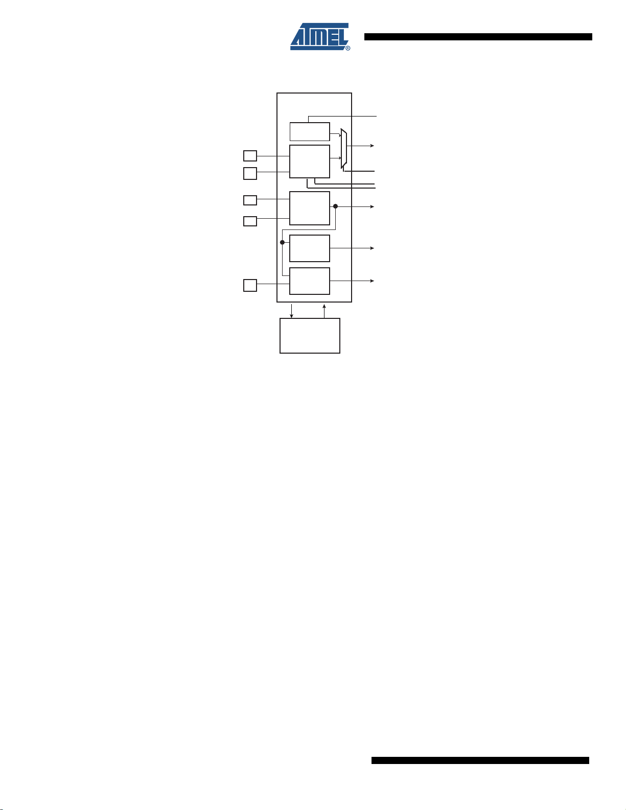
Figure 9-2. Clock Generator Block Diagram
Power
Management
Controller
XIN
XOUT
Main Clock
MAINCK
ControlStatus
PLL and
Divider
PLLRCA
PLL Clock
PLLCK
12M Main
Oscillator
UPLL
(PLLB)
On Chip
RC OSC
Slow Clock
SLCK
XIN32
XOUT32
Slow Clock
Oscillator
Clock Generator
RCEN
HSCK
OSCSEL
OSC32EN
OSC32BYP
9.6 Slow Clock Selection
9.6.1 Description
The AT91SAM9R64/RL64 slow clock can be generated either by an external 32768Hz crystal or
the on-chip RC oscillator. The 32768Hz crystal oscillator can be bypassed to accept an external
slow clock on XIN32.
Configuration is located in the slow clock control register (SCKCR) located at address
0xFFFFFD50 in the backed up part of the system controller and so is preserved while VDDBU is
present.
Refer to the “Clock Generator” section for more details.
9.7 Power Management Controller
The Power Management Controller provides all the clock signals to the system. It provides:
• the Processor Clock PCK
• the Master Clock MCK, in particular to the Matrix and the memory interfaces
• the USB Device HS Clock HSCK
• independent peripheral clocks, typically at the frequency of MCK
• two programmable clock outputs: PCK0 and PCK1
This allows the software control of five flexible operating modes:
• Normal Mode, processor and peripherals running at a programmable frequency
• Idle Mode, processor stopped waiting for an interrupt
• Slow Clock Mode, processor and peripherals running at low frequency
32
AT91SAM9R64/RL64 Preliminary
6289BS–ATARM–07-Oct-08
AT91SAM9R64/RL64 Preliminary
MCK
periph_clk[..]
int
SLCK
MAINCK
PLLCK
Prescaler
/1,/2,/4,...,/64
PCK
Processor
Clock
Controller
Idle Mode
Master Clock Controller
Peripherals
Clock Controller
ON/OFF
SLCK
MAINCK
PLLCK
Prescaler
/1,/2,/4,...,/64
Programmable Clock Controller
pck[..]
ON/OFF
• Standby Mode, mix of Idle and Backup Mode, peripheral running at low frequency, processor
stopped waiting for an interrupt
• Backup Mode, Main Power Supplies off, VDDBU powered by a battery
Figure 9-3. AT91SAM9R64/RL64 Power Management Controller Block Diagram
9.8 Periodic Interval Timer
• Includes a 20-bit Periodic Counter, with less than 1 µs accuracy
• Includes a 12-bit Interval Overlay Counter
• Real Time OS or Linux
9.9 Watchdog Timer
• 16-bit key-protected only-once-Programmable Counter
• Windowed, prevents the processor to be in a dead-lock on the watchdog access
9.10 Real-Time Timer
• Real-Time Timer, allowing backup of time with different accuracies
– 32-bit Free-running back-up Counter
– Integrates a 16-bit programmable prescaler running on slow clock
– Alarm Register capable to generate a wake-up of the system through the Shut Down
Controller
9.11 Real-Time Clock
• Low power consumption
• Full asynchronous design
®
/WindowsCE® compliant tick generator
6289BS–ATARM–07-Oct-08
33

• Two hundred year calendar
• Programmable Periodic Interrupt
• Alarm and update parallel load
• Control of alarm and update Time/Calendar Data In
9.12 General-Purpose Backed-up Registers
• Four 32-bit backup general-purpose registers
9.13 Advanced Interrupt Controller
• Controls the interrupt lines (nIRQ and nFIQ) of the ARM Processor
• Thirty-two individually maskable and vectored interrupt sources
– Source 0 is reserved for the Fast Interrupt Input (FIQ)
– Source 1 is reserved for system peripherals (PIT, RTT, PMC, DBGU, etc.)
– Programmable Edge-triggered or Level-sensitive Internal Sources
– Programmable Positive/Negative Edge-triggered or High/Low Level-sensitive
• One External Sources plus the Fast Interrupt signal
• 8-level Priority Controller
– Drives the Normal Interrupt of the processor
– Handles priority of the interrupt sources 1 to 31
– Higher priority interrupts can be served during service of lower priority interrupt
• Vectoring
– Optimizes Interrupt Service Routine Branch and Execution
– One 32-bit Vector Register per interrupt source
– Interrupt Vector Register reads the corresponding current Interrupt Vector
•Protect Mode
– Easy debugging by preventing automatic operations when protect modeIs are
enabled
•Fast Forcing
– Permits redirecting any normal interrupt source on the Fast Interrupt of the
processor
9.14 Debug Unit
34
AT91SAM9R64/RL64 Preliminary
• Composed of two functions
–Two-pin UART
– Debug Communication Channel (DCC) support
•Two-pin UART
– Implemented features are 100% compatible with the standard Atmel USART
– Independent receiver and transmitter with a common programmable Baud Rate
Generator
– Even, Odd, Mark or Space Parity Generation
– Parity, Framing and Overrun Error Detection
– Automatic Echo, Local Loopback and Remote Loopback Channel Modes
6289BS–ATARM–07-Oct-08

• Debug Communication Channel Support
9.15 Chip Identification
• Chip ID: 0x019B03A0
• JTAG ID: 0x05B2003F
• ARM926 TAP ID: 0x0792603F
9.16 PIO Controllers
• 4 PIO Controllers, PIOA, PIOB, PIOC and PIOD, controlling a maximum of 118 I/O Lines
• Each PIO Controller controls up to 32 programmable I/O Lines
• Fully programmable through Set/Clear Registers
• Multiplexing of two peripheral functions per I/O Line
• For each I/O Line (whether assigned to a peripheral or used as general purpose I/O)
• Synchronous output, provides Set and Clear of several I/O lines in a single write
AT91SAM9R64/RL64 Preliminary
– Support for two PDC channels with connection to receiver and transmitter
– Offers visibility of and interrupt trigger from COMMRX and COMMTX signals from
the ARM Processor’s ICE Interface
– PIOA has 32 I/O Lines
– PIOB has 32 I/O Lines
– PIOC has 32 I/O Lines
– PIOD has 22 I/O Lines
– Input change interrupt
– Glitch filter
– Multi-drive option enables driving in open drain
– Programmable pull up on each I/O line
– Pin data status register, supplies visibility of the level on the pin at any time
10. Peripherals
10.1 Peripheral Mapping
As shown in Figure 8-1, the Peripherals are mapped in the upper 256M bytes of the address
space between the addresses 0xFFFA 0000 and 0xFFFC FFFF.
Each User Peripheral is allocated 16K bytes of address space.
6289BS–ATARM–07-Oct-08
35

10.2 Peripheral Identifiers
The Table 10-1 defines the Peripheral Identifiers of the AT91SAM9R64/RL64. A peripheral identifier is required for the control of the peripheral interrupt with the Advanced Interrupt Controller
and for the control of the peripheral clock with the Power Management Controller.
Table 10-1. AT91SAM9R64/RL64 Peripheral Identifiers
Peripheral ID Peripheral Mnemonic Peripheral Name External Interrupt
0AICAdvanced Interrupt Controller FIQ
1SYSCSystem Controller Interrupt
2PIOAParallel I/O Controller A,
3 PIOB Parallel I/O Controller B
4 PIOC Parallel I/O Controller C
5 PIOD Parallel I/O Controller D
6US0USART 0
7US1USART 1
8US2USART 2
9US3USART 3
10 MCI Multimedia Card Interface
11 TWI0 Two-Wire Interface 0
12 TWI1 Two-Wire Interface 1
13 SPI Serial Peripheral Interface
14 SSC0 Synchronous Serial Controller 0
15 SSC1 Synchronous Serial Controller 1
16 TC0 Timer Counter 0
17 TC1 Timer Counter 1
18 TC2 Timer Counter 2
19 PWMC Pulse Width Modulation Controller
20 TSADCC Touch Screen ADC Controller
21 DMAC DMA Controller
22 UDPHS USB Device High Speed
23 LCDC LCD Controller (AT91SAM9RL64 only)
24 AC97 AC97 Controller
25-30 - Reserved
31 AIC Advanced Interrupt Controller IRQ
Note: Setting AIC, SYSIRQ, LCDC and IRQ bits in the clock set/clear registers of the PMC has no effect.
36
AT91SAM9R64/RL64 Preliminary
6289BS–ATARM–07-Oct-08

10.3 Peripheral Interrupts and Clock Control
10.3.1 System Interrupt
The System Interrupt in Source 1 is the wired-OR of the interrupt signals coming from:
• the SDRAM Controller
• the Debug Unit
• the Periodic Interval Timer
• the Real-time Timer
• the Real-time Clock
• the Watchdog Timer
• the Reset Controller
• the Power Management Controller
The clock of these peripherals cannot be deactivated and Peripheral ID 1 can only be used
within the Advanced Interrupt Controller.
10.3.2 External Interrupts
All external interrupt signals, i.e., the Fast Interrupt signal FIQ or the Interrupt signal IRQ, use a
dedicated Peripheral ID. However, there is no clock control associated with these peripheral IDs.
AT91SAM9R64/RL64 Preliminary
10.4 Peripherals Signals Multiplexing on I/O Lines
The AT91SAM9R64/RL64 features 4 PIO controllers, PIOA, PIOB, PIOC and PIOD, which multiplexes the I/O lines of the peripheral set.
Each PIO Controller controls up to 32 lines. Each line can be assigned to one of two peripheral
functions, A or B. The multiplexing tables in the following paragraphs define how the I/O lines of
the peripherals A and B are multiplexed on the PIO Controllers. The two columns “Function” and
“Comments” have been inserted in this table for the user’s own comments; they may be used to
track how pins are defined in an application.
Note that some peripheral functions which are output only, might be duplicated within the both
tables.
The column “Reset State” indicates whether the PIO Line resets in I/O mode or in peripheral
mode. If I/O is mentioned, the PIO Line resets in input with the pull-up enabled, so that the
device is maintained in a static state as soon as the reset is released. As a result, the bit corresponding to the PIO Line in the register PIO_PSR (Peripheral Status Register) resets low.
If a signal name is mentioned in the “Reset State” column, the PIO Line is assigned to this function and the corresponding bit in PIO_PSR resets high. This is the case for pins controlling
memories, in particular the address lines, which require the pin to be driven as soon as the reset
is released. Note that the pull-up resistor is also enabled in this case.
The AT91SAM9RL64 and AT91SAM9R64 do not have the same peripheral signal multiplexing,
each one follows.
6289BS–ATARM–07-Oct-08
37
10.4.1 AT91SAM9RL64 PIO Multiplexing
10.4.1.1 AT91SAM9RL64 PIO Controller A Multiplexing
Table 10-2. AT91SAM9RL64 Multiplexing on PIO Controller A
PIO Controller A Application Usage
Reset
I/O Line Peripheral A Peripheral B
PA0 MC_DA0 I/O VDDIOP
PA1 MC_CDA I/O VDDIOP
PA2 MC_CK I/O VDDIOP
PA3 MC_DA1 TCLK0 I/O VDDIOP
PA4 MC_DA2 TIOA0 I/O VDDIOP
PA5 MC_DA3 TIOB0 I/O VDDIOP
PA6 TXD0 I/O VDDIOP
PA7 RXD0 I/O VDDIOP
PA8 SCK0 RF1 I/O VDDIOP
PA9 RTS0 RK1 I/O VDDIOP
PA10 CTS0 RK0 I/O VDDIOP
PA11 TXD1 I/O VDDIOP
PA12 RXD1 I/O VDDIOP
PA13 TXD2 TD1 I/O VDDIOP
PA14 RXD2 RD1 I/O VDDIOP
PA15 TD0 I/O VDDIOP
PA16 RD0 I/O VDDIOP
PA17 AD0 I/O VDDANA
State
Power
Supply Function Comments
PA18 AD1 RTS1 I/O VDDANA
PA19 AD2 CTS1 I/O VDDANA
PA20 AD3 SCK3 I/O VDDANA
PA21 DRXD I/O VDDIOP
PA22 DTXD RF0 I/O VDDIOP
PA23 TWD0 I/O VDDIOP
PA24 TWCK0 I/O VDDIOP
PA25 MISO I/O VDDIOP
PA26 MOSI I/O VDDIOP
PA27 SPCK I/O VDDIOP
PA28 NPCS0 I/O VDDIOP
PA29 RTS2 TF1 I/O VDDIOP
PA30 CTS2 TK1 I/O VDDIOP
PA31 NWAIT IRQ I/O VDDIOP
38
AT91SAM9R64/RL64 Preliminary
6289BS–ATARM–07-Oct-08
AT91SAM9R64/RL64 Preliminary
10.4.1.2 AT91SAM9RL64 PIO Controller B Multiplexing
Table 10-3. AT91SAM9RL64 Multiplexing on PIO Controller B
PIO Controller B Application Usage
Reset
I/O Line Peripheral A Peripheral B
PB0 TXD3 I/O VDDIOP
PB1 RXD3 I/O VDDIOP
PB2 A21/NANDALE A21 VDDIOM
PB3 A22/NANDCLE A22 VDDIOM
PB4 NANDOE I/O VDDIOM
PB5 NANDWE I/O VDDIOM
PB6 NCS3/NANDCS I/O VDDIOM
PB7 NCS4/CFCS0 NPCS1 I/O VDDIOM
PB8 CFCE1 PWM0 I/O VDDIOM
PB9 CFCE2 PWM1 I/O VDDIOM
PB10 A25/CFRNW FIQ A25 VDDIOM
PB11 A18 A18 VDDIOM
PB12 A19 A19 VDDIOM
PB13 A20 A20 VDDIOM
PB14 A23 PCK0 A23 VDDIOM
PB15 A24 ADTRG A24 VDDIOM
PB16 D16 I/O VDDIOM
PB17 D17 I/O VDDIOM
State
Power
Supply Function Comments
PB18 D18 I/O VDDIOM
PB19 D19 I/O VDDIOM
PB20 D20 I/O VDDIOM
PB21 D21 I/O VDDIOM
PB22 D22 I/O VDDIOM
PB23 D23 I/O VDDIOM
PB24 D24 I/O VDDIOM
PB25 D25 I/O VDDIOM
PB26 D26 I/O VDDIOM
PB27 D27 I/O VDDIOM
PB28 D28 I/O VDDIOM
PB29 D29 I/O VDDIOM
PB30 D30 I/O VDDIOM
PB31 D31 I/O VDDIOM
6289BS–ATARM–07-Oct-08
39

10.4.1.3 AT91SAM9RL64 PIO Controller C Multiplexing
Table 10-4. AT91SAM9RL64 Multiplexing on PIO Controller C
PIO Controller C Application Usage
Reset
I/O Line Peripheral A Peripheral B
PC0 TF0 I/O VDDIOP
PC1 TK0 LCDPWR I/O VDDIOP
PC2 LCDMOD PWM0 I/O VDDIOP
PC3 LCDCC PWM1 I/O VDDIOP
PC4 LCDVSYNC I/O VDDIOP
PC5 LCDHSYNC I/O VDDIOP
PC6 LCDDOTCK I/O VDDIOP
PC7 LCDDEN I/O VDDIOP
PC8 LCDD0 LCDD2 I/O VDDIOP
PC9 LCDD1 LCDD3 I/O VDDIOP
PC10 LCDD2 LCDD4 I/O VDDIOP
PC11 LCDD3 LCDD5 I/O VDDIOP
PC12 LCDD4 LCDD6 I/O VDDIOP
PC13 LCDD5 LCDD7 I/O VDDIOP
PC14 LCDD6 LCDD10 I/O VDDIOP
PC15 LCDD7 LCDD11 I/O VDDIOP
PC16 LCDD8 LCDD12 I/O VDDIOP
PC17 LCDD9 LCDD13 I/O VDDIOP
State
Power
Supply Function Comments
PC18 LCDD10 LCDD14 I/O VDDIOP
PC19 LCDD11 LCDD15 I/O VDDIOP
PC20 LCDD12 LCDD18 I/O VDDIOP
PC21 LCDD13 LCDD19 I/O VDDIOP
PC22 LCDD14 LCDD20 I/O VDDIOP
PC23 LCDD15 LCDD21 I/O VDDIOP
PC24 LCDD16 LCDD22 I/O VDDIOP
PC25 LCDD17 LCDD23 I/O VDDIOP
PC26 LCDD18 I/O VDDIOP
PC27 LCDD19 I/O VDDIOP
PC28 LCDD20 I/O VDDIOP
PC29 LCDD21 TIOA1 I/O VDDIOP
PC30 LCDD22 TIOB1 I/O VDDIOP
PC31 LCDD23 TCLK1 I/O VDDIOP
40
AT91SAM9R64/RL64 Preliminary
6289BS–ATARM–07-Oct-08
AT91SAM9R64/RL64 Preliminary
10.4.1.4 AT91SAM9RL64 PIO Controller D Multiplexing
Table 10-5. AT91SAM9RL64 Multiplexing on PIO Controller D
PIO Controller D Application Usage
Reset
I/O Line Peripheral A Peripheral B Comments
PD0 NCS2 I/O VDDIOP
PD1 AC97_FS I/O VDDIOP
PD2 AC97_CK SCK1 I/O VDDIOP
PD3 AC97_TX CTS3 I/O VDDIOP
PD4 AC97_RX RTS3 I/O VDDIOP
PD5 DTXD PWM2 I/O VDDIOP
PD6 AD4 I/O VDDANA
PD7 AD5 I/O VDDANA
PD8 NPCS2 PWM3 I/O VDDIOP
PD9 SCK2 NPCS3 I/O VDDIOP
PD10 TWD1 TIOA2 I/O VDDIOP
PD11 TWCK1 TIOB2 I/O VDDIOP
PD12 PWM2 PCK1 I/O VDDIOP
PD13 NCS5/CFCS1 NPCS3 I/O VDDIOP
PD14 DSR0 PWM0 I/O VDDIOP
PD15 DTR0 PWM1 I/O VDDIOP
PD16 DCD0 PWM2 I/O VDDIOP
PD17 RI0 I/O VDDIOP
State
Power
Supply Function Comments
PD18 PWM3 I/O VDDIOP
PD19 PCK0 I/O VDDIOP
PD20 PCK1 I/O VDDIOP
PD21 TCLK2 I/O VDDIOP
6289BS–ATARM–07-Oct-08
41

10.4.2 AT91SAM9R64 PIO Multiplexing
Note: In Table 10-6, Table 10-7, Table 10-8 and Table 10-9, shaded cells indicate I/O lines that are NOT available on the
AT91SAM9R64.
10.4.2.1 AT91SAM9R64 PIO Controller A Multiplexing
Table 10-6. AT91SAM9R64 Multiplexing on PIO Controller A
PIO Controller A Application Usage
Reset
I/O Line Peripheral A Peripheral B
PA0 MC_DA0 I/O VDDIOP
PA1 MC_CDA I/O VDDIOP
PA2 MC_CK I/O VDDIOP
PA3 MC_DA1 TCLK0 I/O VDDIOP
PA4 MC_DA2 TIOA0 I/O VDDIOP
PA5 MC_DA3 TIOB0 I/O VDDIOP
PA6 TXD0 I/O VDDIOP
PA7 RXD0 I/O VDDIOP
PA 8 NA NA Reserved
PA 9 NA NA Reserved
PA10 CTS0 RK0 I/O VDDIOP
PA11 TXD1 I/O VDDIOP
PA12 RXD1 I/O VDDIOP
PA13 TXD2 I/O VDDIOP
PA14 RXD2 I/O VDDIOP
PA15 TD0 I/O VDDIOP
PA16 RD0 I/O VDDIOP
PA17 AD0 I/O VDDIOP
PA18 AD1 RTS1 I/O VDDIOP
PA19 AD2 CTS1 I/O VDDIOP
PA 20 NA NA Reserved
PA21 DRXD I/O VDDIOP
PA22 DTXD RF0 I/O VDDIOP
PA23 TWD0 I/O VDDIOP
PA24 TWCK0 I/O VDDIOP
PA25 MISO I/O VDDIOP
PA26 MOSI I/O VDDIOP
PA27 SPCK I/O VDDIOP
PA28 NPCS0 I/O VDDIOP
PA 29 NA NA Reserved
PA 30 NA NA Reserved
PA31 NWAIT IRQ I/O VDDIOP
State
Power
Supply Function Comments
42
AT91SAM9R64/RL64 Preliminary
6289BS–ATARM–07-Oct-08

AT91SAM9R64/RL64 Preliminary
10.4.2.2 AT91SAM9R64 PIO Controller B Multiplexing
Table 10-7. AT91SAM9R64 Multiplexing on PIO Controller B
PIO Controller B Application Usage
Reset
I/O Line Peripheral A Peripheral B
PB0 TXD3 I/O VDDIOP
PB1 RXD3 I/O VDDIOP
PB2 A21/NANDALE A21 VDDIOM
PB3 A22/NANDCLE A22 VDDIOM
PB4 NANDOE I/O VDDIOM
PB5 NANDWE I/O VDDIOM
PB6 NCS3/NANDCS I/O VDDIOM
PB7 NCS4/CFCS0 NPCS1 I/O VDDIOM
PB8 CFCE1 PWM0 I/O VDDIOM
PB9 CFCE2 PWM1 I/O VDDIOM
PB10 A25/CFRNW FIQ A25 VDDIOM
PB11 A18 A18 VDDIOM
PB12 A19 A19 VDDIOM
PB13 A20 A20 VDDIOM
PB14 A23 PCK0 A23 VDDIOM
PB15 A24 ADTRG A24 VDDIOM
PB16-
PB31
NA NA Reserved
State
Power
Supply Function Comments
6289BS–ATARM–07-Oct-08
43

10.4.2.3 AT91SAM9R64 PIO Controller C Multiplexing
Table 10-8. AT91SAM9R64 Multiplexing on PIO Controller C
PIO Controller C Application Usage
Reset
I/O Line Peripheral A Peripheral B
PC0 TF0 I/O VDDIOP
PC1 TK0 I/O VDDIOP
PC2-
PC31
NA NA Reserved
State
Power
Supply Function Comments
10.4.2.4 AT91SAM9R64 PIO Controller D Multiplexing
Table 10-9. AT91SAM9R64 Multiplexing on PIO Controller D
PIO Controller D Application Usage
Reset
I/O Line Peripheral A Peripheral B Comments
PD0-
PD17
PD18 PWM3 I/O VDDIOP
PD19 PCK0 I/O VDDIOP
PD20 PCK1 I/O VDDIOP
PD21 TCLK2 I/O VDDIOP
NA NA Reserved
State
Power
Supply Function Comments
44
AT91SAM9R64/RL64 Preliminary
6289BS–ATARM–07-Oct-08

11. Embedded Peripherals Overview
11.1 Serial Peripheral Interface (SPI)
• Supports communication with serial external devices
– Four chip selects with external decoder support allow communication with up to 15
peripherals
– Serial memories, such as DataFlash and 3-wire EEPROMs
– Serial peripherals, such as ADCs, DACs, LCD Controllers, CAN Controllers and
Sensors
– External co-processors
• Master or slave serial peripheral bus interface
– 8- to 16-bit programmable data length per chip select
– Programmable phase and polarity per chip select
– Programmable transfer delays between consecutive transfers and between clock
and data per chip select
– Programmable delay between consecutive transfers
– Selectable mode fault detection
• Very fast transfers supported
– Transfers with baud rates up to MCK
– The chip select line may be left active to speed up transfers on the same device
AT91SAM9R64/RL64 Preliminary
11.2 Two-wire Interface (TWI)
• Compatibility with standard two-wire serial memory
• One, two or three bytes for slave address
• Sequential read/write operations
• Supports either master or slave modes
• Compatible with Standard Two-wire Serial Memories
• Master, Multi-master and Slave Mode Operation
• Bit Rate: Up to 400 Kbits
• General Call Supported in Slave mode
• Connection to Peripheral DMA Controller (PDC) Channel Capabilities Optimizes Data
Transfers in Master Mode Only
– One Channel for the Receiver, One Channel for the Transmitter
– Next Buffer Support
11.3 USART
• Programmable Baud Rate Generator
• 5- to 9-bit full-duplex synchronous or asynchronous serial communications
– 1, 1.5 or 2 stop bits in Asynchronous Mode or 1 or 2 stop bits in Synchronous Mode
– Parity generation and error detection
– Framing error detection, overrun error detection
– MSB- or LSB-first
6289BS–ATARM–07-Oct-08
45

– Optional break generation and detection
– By 8 or by-16 over-sampling receiver frequency
– Hardware handshaking RTS-CTS
– Receiver time-out and transmitter timeguard
– Optional Multi-drop Mode with address generation and detection
– Optional Manchester Encoding
• RS485 with driver control signal
• ISO7816, T = 0 or T = 1 Protocols for interfacing with smart cards
– NACK handling, error counter with repetition and iteration limit
• IrDA modulation and demodulation
– Communication at up to 115.2 Kbps
• Test Modes
– Remote Loopback, Local Loopback, Automatic Echo
11.4 Serial Synchronous Controller (SSC)
• Provides serial synchronous communication links used in audio and telecom applications
(with CODECs in Master or Slave Modes, I
• Contains an independent receiver and transmitter and a common clock divider
• Offers a configurable frame sync and data length
• Receiver and transmitter can be programmed to start automatically or on detection of
different event on the frame sync signal
• Receiver and transmitter include a data signal, a clock signal and a frame synchronization
signal
2
S, TDM Buses, Magnetic Card Reader, etc.)
11.5 AC97 Controller
• Compatible with AC97 Component Specification V2.2
• Capable to Interface with a Single Analog Front end
• Three independent RX Channels and three independent TX Channels
• Time Slot Assigner allowing to assign up to 12 time slots to a channel
• Channels support mono or stereo up to 20 bit sample length
11.6 Timer Counter (TC)
• Three 16-bit Timer Counter Channels
• Wide range of functions including:
– One RX and one TX channel dedicated to the AC97 Analog Front end control
– One RX and one TX channel for data transfers, associated with a PDC
– One RX and one TX channel for data transfers with no PDC
– Variable sampling rate AC97 Codec Interface (48KHz and below)
– Frequency Measurement
– Event Counting
– Interval Measurement
– Pulse Generation
46
AT91SAM9R64/RL64 Preliminary
6289BS–ATARM–07-Oct-08

AT91SAM9R64/RL64 Preliminary
–Delay Timing
– Pulse Width Modulation
– Up/down Capabilities
• Each channel is user-configurable and contains:
– Three external clock inputs
– Five internal clock inputs
– Two multi-purpose input/output signals
• Two global registers that act on all three TC Channels
11.7 Pulse Width Modulation Controller (PWM)
• 4 channels, one 16-bit counter per channel
• Common clock generator, providing Thirteen Different Clocks
– A Modulo n counter providing eleven clocks
– Two independent Linear Dividers working on modulo n counter outputs
• Independent channel programming
– Independent Enable Disable Commands
– Independent Clock Selection
– Independent Period and Duty Cycle, with Double Bufferization
– Programmable selection of the output waveform polarity
– Programmable center or left aligned output waveform
11.8 Multimedia Card Interface (MCI)
• Compatibility with MultiMedia Card Specification Version 3.31
• Compatibility with SD Memory Card Specification Version 1.0
• Compatibility with SDIO Specification Version V1.0.
• Cards clock rate up to Master Clock divided by 2
• Embedded power management to slow down clock rate when not used
• MCI has one slot supporting
– One MultiMediaCard bus (up to 30 cards) or
– One SD Memory Card
– One SDIO Card
• Support for stream, block and multi-block data read and write
11.9 USB High Speed Device Port (UDPHS)
• USB V2.0 high-speed compliant, 480 MBits per second
• Embedded USB V2.0 UTMI+ high-speed transceiver
• Embedded 4K-byte dual-port RAM for endpoints
• Embedded 6 channels DMA controller
• Suspend/Resume logic
• Up to 3 banks for isochronous and bulk endpoints
• Seven endpoints:
6289BS–ATARM–07-Oct-08
47

– Endpoint 0: 64 bytes, 1 bank mode
– Endpoint 1 & 2: 1024 bytes, 2 banks mode, HS isochronous capable, DMA
– Endpoint 3 & 4: 1024bytes, 3 banks mode, DMA
– Endpoint 5 & 6: 1024 bytes, 3 banks mode, HS isochronous capable, DMA
11.10 LCD Controller (LCDC)
• Single and Dual scan color and monochrome passive STN LCD panels supported
• Single scan active TFT LCD panels supported.
• 4-bit single scan, 8-bit single or dual scan, 16-bit dual scan STN interfaces supported
• Up to 24-bit single scan TFT interfaces supported
• Up to 16 gray levels for mono STN and up to 4096 colors for color STN displays
• 1, 2 bits per pixel (palletized), 4 bits per pixel (non-palletized) for mono STN
• 1, 2, 4, 8 bits per pixel (palletized), 16 bits per pixel (non-palletized) for color STN
• 1, 2, 4, 8 bits per pixel (palletized), 16, 24 bits per pixel (non-palletized) for TFT
• Single clock domain architecture
• Resolution supported up to 2048 x 2048
11.11 Touch Screen Analog-to-digital Converter (TSADCC)
• 6-channel ADC
• Support 4-wire resistive Touch Screen
• 10-bit 384 Ksamples/sec. Successive Approximation Register ADC
• -3/+3 LSB Integral Non Linearity, -2/+2 LSB Differential Non Linearity
• Integrated 6-to-1 multiplexer, offering eight independent 3.3V analog inputs
• External voltage reference for better accuracy on low voltage inputs
• Individual enable and disable of each channel
• Multiple trigger sources
– Hardware or software trigger
– External trigger pin
– Timer Counter 0 to 2 outputs TIOA0 to TIOA2 trigger
• Sleep Mode and conversion sequencer
– Automatic wakeup on trigger and back to sleep mode after conversions of all
enabled channels
48
AT91SAM9R64/RL64 Preliminary
6289BS–ATARM–07-Oct-08
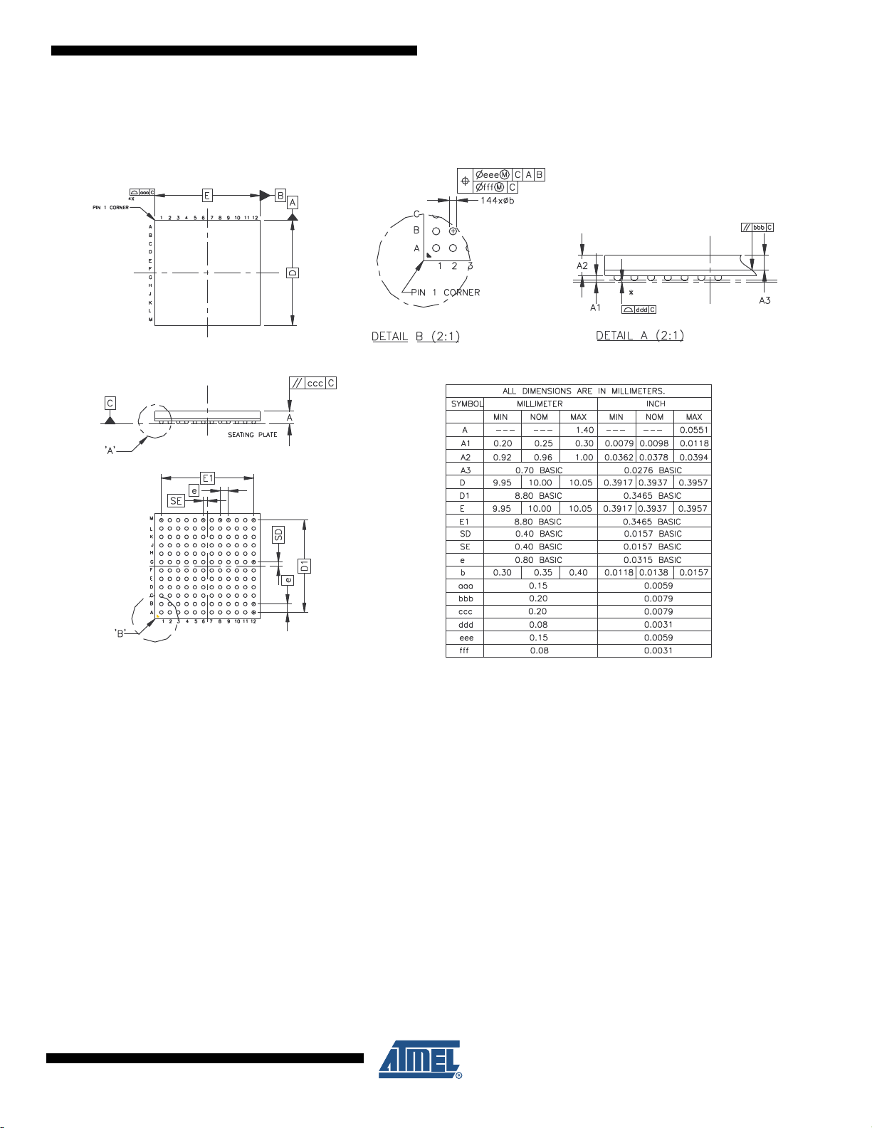
12. Package Drawings
Figure 12-1. 144-ball LFBGA Package Drawing
AT91SAM9R64/RL64 Preliminary
6289BS–ATARM–07-Oct-08
49
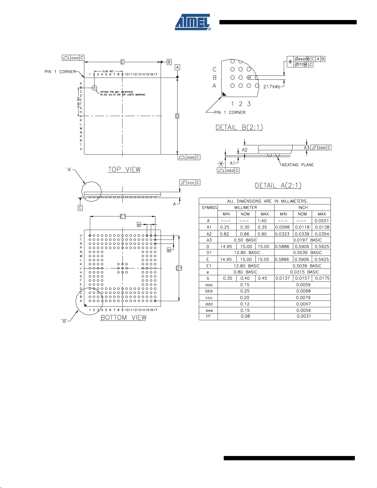
Figure 12-2. 217-ball LFBGA Package Drawing
50
AT91SAM9R64/RL64 Preliminary
6289BS–ATARM–07-Oct-08
13. Ordering Information
Table 13-1. AT91SAM9R64/RL64 Ordering Information
Ordering Code Package Package Type Temperature Operating Range
AT91SAM9R64-CU LFBGA144 Green
AT91SAM9RL64-CU LFBGA217 Green
AT91SAM9R64/RL64 Preliminary
Industrial
-40°C to 85°C
6289BS–ATARM–07-Oct-08
51
Revision History
Doc. Rev Comments
“Features”“Debug Unit (DBGU)” on page 2, updated
Figure 8-1 “AT91SAM9R64/RL64 Memory Mapping”, Internal Memory Mapping updated.
Table 7-2, “List of Bus Matrix Slaves”, Table 7-3, “AT91SAM9R64/RL64 Master to Slave Access”, Slave
3 updated.
6289BS
6289AS First issue
Section 5.1 “Power Supplies”, updated with caution on VDDCORE and VDDIO constraints
Section 5.1.1 “USB Power Supply Considerations” and Figure 5-1 added to datasheet.
Section 5.2 “Power Consumption”, first two sentences updated.
Table 3-1, “Signal Description List”, additional comments on BMS.
SHDN comments updated.
Table 10-3 and Table 10-7 PB8, PB9 Peripheral A column: typos corrected, “CFCE1”, “CFCE2”.
Change
Request
Ref.
5846
5276
5291
5420
5388
5423
rfo
5788
52
AT91SAM9R64/RL64 Preliminary
6289BS–ATARM–07-Oct-08
 Loading...