


AT91SAM9G20-EK Evaluation Board
....................................................................................................................
User Guide
6413C–ATARM–18-Feb-09

1-2 AT91SAM9G20-EK Evaluation Board User Guide
6413C–ATARM–18-Feb-09

Table of Contents
Section 1
Overview .................................................................................................................... 1-1
1.1 Scope................................................................................................................................. 1-1
1.2 Deliverables ....................................................................................................................... 1-1
1.3 AT91SAM9G20-EK Evaluation Board ............................................................................... 1-1
Section 2
Setting Up the AT91SAM9G20-EK Board.................................................................. 2-1
2.1 Electrostatic Warning ......................................................................................................... 2-1
2.2 Requirements..................................................................................................................... 2-1
2.3 Layout ................................................................................................................................ 2-2
2.4 Powering Up the Board...................................................................................................... 2-4
2.5 Backup Power Supply........................................................................................................ 2-4
2.6 Getting Started................................................................................................................... 2-4
2.7 AT91SAM9G20-EK Block Diagram ................................................................................... 2-5
Section 3
Board Description....................................................................................................... 3-1
3.1 AT91SAM9G20 Microcontroller ......................................................................................... 3-1
3.2 AT91SAM9G20 Block Diagram ......................................................................................... 3-4
3.3 Microcontroller ................................................................................................................... 3-5
3.4 Memory .............................................................................................................................. 3-5
3.5 Clock Circuitry.................................................................................................................... 3-5
3.6 Reset Circuitry ................................................................................................................... 3-5
3.7 Shutdown Controller ..........................................................................................................3-5
3.8 Power Supply Circuitry.......................................................................................................3-5
3.9 Remote Communication .................................................................................................... 3-5
3.10 Audio Stereo Interface ....................................................................................................... 3-6
3.11 User Interface .................................................................................................................... 3-6
3.12 Debug Interface ................................................................................................................. 3-6
3.13 Expansion Slot ................................................................................................................... 3-6
3.14 PIO Usage ......................................................................................................................... 3-7
Section 4
Configuration ..............................................................................................................4-1
4.1 Jumpers ............................................................................................................................. 4-1
4.2 JTAG/ICE........................................................................................................................... 4-2
AT91SAM9G20-EK Evaluation Board User Guide i
6413C–ATARM–18-Feb-09

Table of Contents (Continued)
4.3 Microcontroller Clock ......................................................................................................... 4-2
4.4 Memory .............................................................................................................................. 4-2
4.5 Ethernet ............................................................................................................................. 4-3
4.6 Miscellaneous .................................................................................................................... 4-3
Section 5
Schematics................................................................................................................. 5-1
5.1 Schematics ........................................................................................................................ 5-1
Section 6
Errata..........................................................................................................................6-1
6.1 Wrong Silkscreen of BB and 1.0V on the Board ................................................................ 6-1
6.2 Choice of an Oscillator Capacitance.................................................................................. 6-1
6.3 SD Card Slots and Booting Capability ............................................................................... 6-1
Section 7
Revision History .........................................................................................................7-1
7.1 Revision History ................................................................................................................. 7-1
ii AT91SAM9G20-EK Evaluation Board User Guide
6413C–ATARM–18-Feb-09

1.1 Scope
The AT91SAM9G20-EK Evaluation Kit enables the evaluation of and code development for applications
running on an AT91SAM9G20 device. This guide focuses on the AT91SAM9G20-EK board as an evaluation platform. The board supports the AT91SAM9G20 in a 217-ball LFBGA RoHS-compliant Package.
1.2 Deliverables
The AT91SAM9G20-EK package contains the following items:
an AT91SAM9G20-EK board
a universal input AC/DC power supply with US and Europe plug adapter
one A/B-type USB cable
one serial RS232 cable
one RJ45 crossed Ethernet cable
one CD-ROM that allows the user to begin evaluating the AT91 ARM
quickly
one 3V Lithium battery
Section 1
Overview
®
Thumb® 32-bit microcontroller
1.3 AT91SAM9G20-EK Evaluation Board
The board is equipped with an AT91SAM9G20 microcontroller together with the following:
64 Mbytes of SDRAM memory
256 Mbytes of NAND Flash memory
one Atmel
one Atmel TWI serial EEPROM
one USB Device port interface
two USB Host port interfaces
one DBGU serial communication port
one complete MODEM serial communication port
one additional serial communication port with RTS/CTS handshake control
JTAG/ICE debug interface
one PHY Ethernet 100-base TX with three status LEDs
one on-board Audio DAC
one Power LED and one general-purpose LED
AT91SAM9G20-EK Evaluation Board User Guide 1-1
®
serial DataFlash
®
6413C–ATARM–18-Feb-09

Overview
two user-input push buttons
one Wakeup-input push button
one reset push button
two DataFlash SD/MMC card slots
four expansion connectors (PIOA, PIOB, PIOC, IMAGE SENSOR)
one BGA-like EBI expansion footprint connector
one Lithium Coin Cell Battery Retainer for 12 mm cell size
1-2 AT91SAM9G20-EK Evaluation Board User Guide
6413C–ATARM–18-Feb-09

2.1 Electrostatic Warning
The AT91SAM9G20-EK evaluation board is shipped in protective anti-static packaging. The board must
not be subjected to high electrostatic potentials. A grounding strap or similar protective device should be
worn when handling the board. Avoid touching the component pins or any other metallic element.
2.2 Requirements
In order to set up the AT91SAM9G20-EK evaluation board, the following items are needed:
the AT91SAM9G20-EK evaluation board itself,
AC/DC power adapter (5V at 2A), 2.1 mm by 5.5 mm.
Section 2
Setting Up the AT91SAM9G20-EK Board
AT91SAM9G20-EK Evaluation Board User Guide 2-1
6413C–ATARM–18-Feb-09
Setting Up the AT91SAM9G20-EK Board
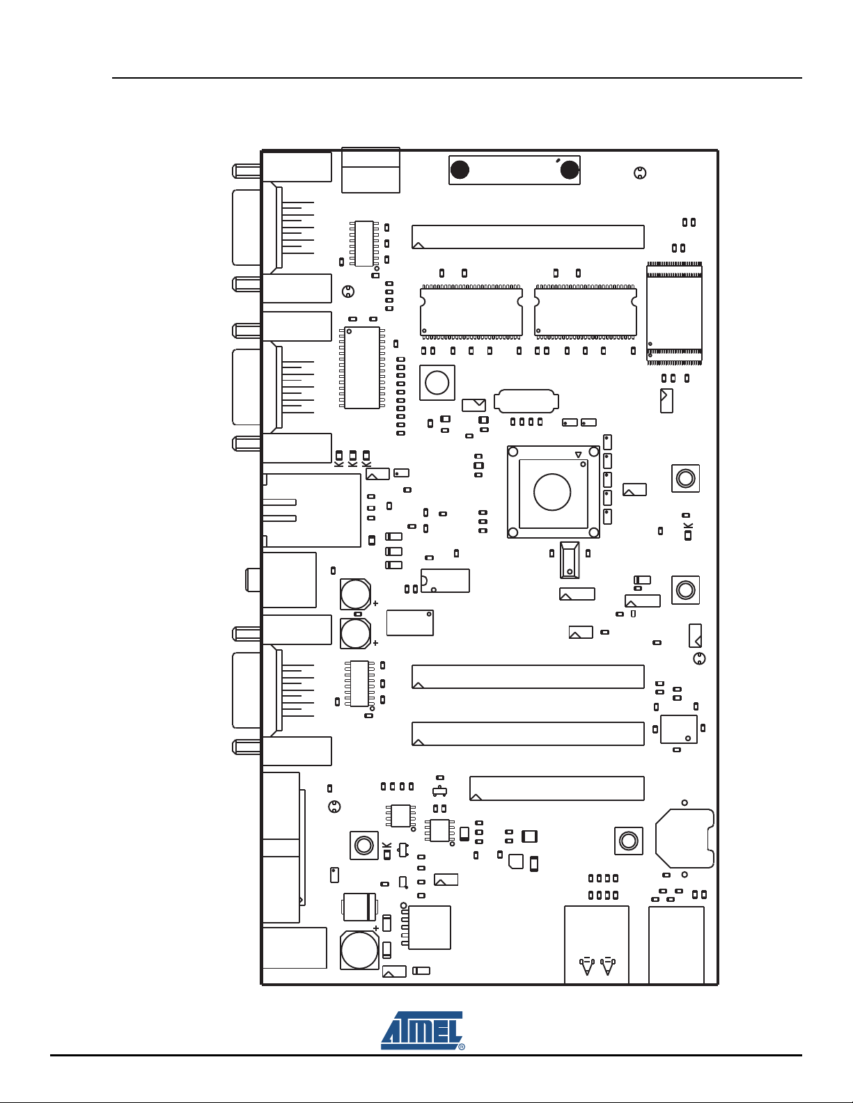
2.3 Layout
Figure 2-1. Top View
J18
J20
J17
J31
J25
TP4
1
TP7
J24
5
C115
TP3
1
5
DS4
J14
R15
J4
1
C104
5
R64
TP1
BP1
RR1
J5
C116
C127
MN14
DS3
L3
C17
C16
MN12
CR1
MN13
C121
DS2
J15
C90
C102
C95
C146
C105
R47
R3
DS1
C2
C117 C118
C114
R155
C122
C94
C107
C106
C103
R88
R85
R83
R86
R62
R151
R156
MN10
Q1
Q2
R46
R107
R106
R98
R101
R103
R104
R105
R96
R95
R94
R57
C93
C99
R5R9
C14R10
C81
RR6
C101
R150
MN2
MN1
MN8
R22
S8
C87
J23
J26
R164
C75
R50
C78
J8
L2
R45
R56
Y3
R168
MN15
J3
R49
R163
C76
C77
R21
Q3
C69
C68
MN7
R31
C72
RR21
RR17
RR10
RR11RR20
J12
TP5
TP6
C42
R26
J10
C47
MN5
S2
S5
R28
L4
R44
C80
L5
R120
R119
R124
R32
J6
R43
C74
C79
Y1
R18
C23
R20
C24
RR4
RR19
C73
C70
C71
MN4
C25
Y2
C26
J9
J7
J28
R166
D1
K
R169
R165
R167
C12
C11
R7
MN3
R11
C15
C110
R70
C111
R71
C112
R77
C113
R78
BP2
R87
J16
J1
C1
C3
J2
C4
C84
MN6A1
MN6B1
R38
J34
BP4
R108
R158
R154
R157
C82
R25
C123
R171
C83
R153
DS5
R159
R160
MN9
C85
J11
C124
C119
J19
R170
C148
R39
TP2
R37
R81
BP3
J33
R42
R84
2-2 AT91SAM9G20-EK Evaluation Board User Guide
6413C–ATARM–18-Feb-09
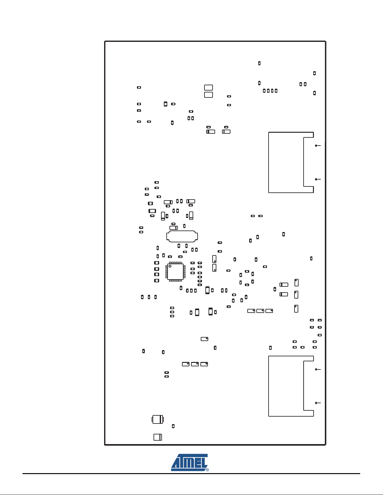
Figure 2-2. Bottom View
S1
S3
R13
R14R16
R63
C126
R136
R137
Setting Up the AT91SAM9G20-EK Board
C108
C120
C109
R74
R66
R67
R19 R17
C43
RR3RR2
R29
R76
R89
R90
R82
J13
R24
R118
RR9
C37
R27
RR18
C38
RR16
R173
R175
R176
R172
R174
R34
R35
S6
R41
R33
F1
F2
C50
RR14
RR15 RR13RR12
C5 C6
C130 C133
C131
R125
R126
RR7
C44
RR8
C35
C51
C48
R30
C21
C27
C28
C22
S4
C49
R23
R109
C32
C34
C40
C45
C33
C46
C41
C39
RR5
C36
R4
R1
R72 R73
R69
R68
R75
L1
C18
C136
R12
C137
C139
C86
C140
C141
R128
C138
C147
R161
R162
C132
R8
R6
R2
C145
C144
C143
C142
R48
Y4
C88
C125
C89
S7
R132
C96
MN11
C98
R134
C30
R133
R135
R127
R123
R55
R131
C97
R130
R122
R129
R60
R121
C31
R58
C92
R91
R92
R93
R65
C91
R53
R52 R54
R51
R61
R59
R79
R80
J35
CR2
C135
C134
AT91SAM9G20-EK Evaluation Board User Guide 2-3
6413C–ATARM–18-Feb-09

Setting Up the AT91SAM9G20-EK Board
2.4 Powering Up the Board
The AT91SAM9G20-EK requires 5V DC (±5%). DC power is supplied to the board via the 2.1 mm by 5.5
mm socket J1. Coaxial plug center positive standard.
2.5 Backup Power Supply
The user can plug in a battery (3V Lithium Battery CR1225 or equivalent) in order to permanently power
the backup part of the device. In this case, J10 configuration must be set in position 1, 2. Refer to Sec-
tion 4.1 ”Jumpers”.
2.6 Getting Started
The AT91SAM9G20-EK evaluation board is delivered with a CD-ROM containing all necessary information and step-by-step procedures for working with the most common development tools.
2-4 AT91SAM9G20-EK Evaluation Board User Guide
6413C–ATARM–18-Feb-09
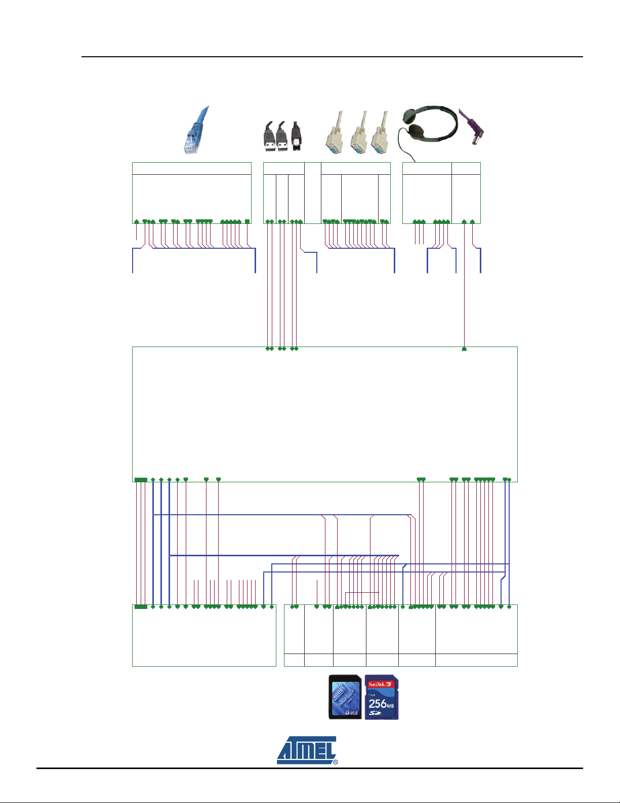
2.7 AT91SAM9G20-EK Block Diagram
PIO
ET
X
C
K
/
R
E
F
CLK
ET
X
0
ET
X
1
ETXEN
ERX1
ERX0
ERXDV
ERXER
EMDC
EMDIO
ET
X
2
ET
X
3
ERX2
ERX3
ET
X
ER
ERXCK
E
C
RS
ECO
L
MCDB2
SPI0_NPCS0 MCDB3
S
P
I
0
_MOSI MCCDB
M
C
CK
SPI0_MISO MCDB0
MCDB1
SDRAM
NANFL
ASH
DAC
WM8
7
31
5VDC
DBGU
H
O
ST
A
HOST B
USB
D
EVI
C
E
C
O
M1
C
O
M
0
RS232
CA
R
D
R
EA
DER
DBGU_RXD
D
B
GU_TX
D
10/100 Mbps FAST ETHERNET
EEPROM
SERIAL
PIO
P
I
O
P
I
O
PIO
TWD
TWCK
SPI0_N
P
C
S
1
SP
I
0_SPCK
DATAFLASH
SERIAL
DATAFLASH
MCIB
SH
E
E
T 2
SHEET 5
SHEET 6
SH
EE
T 7
PA23
/
TWD
PA24
/
T
WC
K
TF0
TK0
TD0
PCK0
SPI1
_N
P
C
S
0
DATAFLASH
MCIA
C
A
RD
READER
(B
O
OT
)
MCDA0
MCDA1
M
CDA2MCDA3MCCKMCCD
A
RAS
C
A
S
S
D
A
1
0
S
D
W
E
S
D
CS_
NC
S
1
S
D
CK
S
D
CKE
NBS1
NBS
3
PB
[
0..
3
1]
PB
9
PA
1
7
PA
1
9
P
B
0
PA
1
1
PA
1
0
PA25
PA26
PA
2
2
PA
2
7
PA
2
8
PA
2
9
PA
1
3
PA
1
2
PA16
P
A
15
P
A
14
PA20
PA21
PA
1
8
PA
[
0.
.3
1
]
NRST
N
AN
D
OE
N
AN
D
WE
A22
A
21
D[
0
..31]
A
1
6
A
1
7
A
[
0
..
1
4
]
A
[
0
.
.2
2
]
NCS0
NRST
CF
W
E_
NWE_
NW
R0
CFOE_N
R
D
RAS
CAS
S
D
A10
SDWE
S
D
C
S
_
NCS1
S
D
CK
S
D
CKE
NBS1
NBS3
NANDOE
NANDWE
PB
[
0.
.3
1]
DDP
HDPA
HDM
A
HDPB
HDMBDD
M
PB15
PB
[
0
..31]
PB
1
4
PA0P
A5
PA[0..
3
1]
PA4P
A3
PA8
P
A1
P
C
1
4
P
C
1
3
PC[0..15]
PB
26
PB
2
3
PB
2
5
PB28
PB6
PB7
P
B
29
PB4
PB5
PB
27
PB
2
4
PB
2
2
D
[0
..1
5
]
PC[0
.
.15]
PC5
NRST
PC11
PA2
P
A2
3
P
A2
4
PC9
PB17
PB18
P
B
16
P
C
[0.
.
15
]
PC1
PB
[
0.
.3
1
]
PA
2
3
PA
2
4
PB
3
PA6
PA9
PA
1
0
PA
1
1
PA7P
C
2
PB
[
0.
.3
1
]
PA
8
SE
R
IA
L
INTERF
A
CES
0
5
COMMUNICAT
IO
N
HDMA
HDMB
DD
M
D
DP
HDPA
HDPB
PB29
PB26
PB4
PB28
PB6
PB5
PB7
PB2
5
PC5
PB14
PB2
3
PB15
PB22PB27
PB24
R
MII_MII
ET
HERNET
03
RMII_
M
II ETHERNET
NRST
PA28PA1
8
PA1
2
PA2
2
PA1
3
PA14
PA1
0
PA15
PA1
1
PA17PA25
PA26
PA20
PA19
PB0
PA27
PA2
9
PA21
PA16
M
EM
OR
Y
03 - MEMORY
CAS
SDWESDC
S_
NC
S1
SDCKECFIOR_NBS1_NWR1
SDC
K
SDA10D
[
0..
3
1
]
RAS
C
F
I
O
W
_
NBS3
_
N
W
R3
N
RST
NANDOE
NAN
D
WE
PC13
PC14
A21
A22
PA0
PA5
PA4
PA8
PA3
PA2
PA1
PC
11
A16A1
7
A[0
..
1
4
]
D[
0
..1
5
]
PA24
PA2
3
PC9
PA6
PA9
PA1
0
PA11PA8
PA7
PC2
EXPANSION
_
Users I
n
terfac
e
s
06
- EX
P
A
N
S
I
O
N
C
O
N
NECTORS
PA[
0..31]
A[
0..
2
2
]
D[0..31]
PB[0.
.
31]
C
AS
SDWE
N
ANDOE
SDCS_NCS1
NRST
SDCKESDC
K
CFIOR_NBS1_NWR1
N
ANDWE
SDA10
R
AS
CFIOW_NBS3_NWR3
NCS0
CFW
E_
NWE_N
W
R
0
C
F
O
E_NRD
PC[0..15]
AVD
D
AGN
D
VR
EF
P
PO
WER SUPPL
Y
01 -
PO
WER SUPPL
Y
SHD
N
PB9
PB16
PB17
PA23
PC
1
PB18
PA24
PB3
A
T
9
1
SA
M
9
G
20-CU
02
- AT91SAM
9
G20-CU
PA[0..3
1
]
A[
0
..
2
2
]
PB[0
.
.3
1
]
PC[0..15]
D[0..31]
CAS
SD
W
E
HDMA
HDMB
SD
C
S_
N
C
S1
NRST
NCS0
C
F
WE_N
W
E_
N
W
R0
SD
CKE
DD
M
CFIOR_NBS1_N
W
R1
SD
CK
SDA1
0
DD
P
RAS
HDPA
C
F
IO
W
_NBS3
_
N
W
R3
HDPB
NANDOE
CFO
E_
NR
D
NAN
D
WE
SHDN
AVD
D
AGN
D
VREFP
Figure 2-3. AT91SAM9G20-EK Block Diagram
Setting Up the AT91SAM9G20-EK Board
AT91SAM9G20-EK Evaluation Board User Guide 2-5
6413C–ATARM–18-Feb-09

Setting Up the AT91SAM9G20-EK Board
2-6 AT91SAM9G20-EK Evaluation Board User Guide
6413C–ATARM–18-Feb-09

3.1 AT91SAM9G20 Microcontroller
• Incorporates the ARM926EJ-S
– DSP Instruction Extensions, ARM Jazelle
– 32-KByte Data Cache, 32-KByte Instruction Cache, Write Buffer
– CPU Frequency 400 MHz
– Memory Management Unit
– EmbeddedICE
• Additional Embedded Memories
– One 64-KByte Internal ROM, Single-cycle Access at Maximum Matrix Speed
– Two 16-KByte Internal SRAM, Single-cycle Access at Maximum Matrix Speed
• External Bus Interface (EBI)
– Supports SDRAM, Static Memory, ECC-enabled NAND Flash and CompactFlash
• USB 2.0 Full Speed (12 Mbits per second) Device Port
– On-chip Transceiver, 2,432-byte Configurable Integrated DPRAM
• USB 2.0 Full Speed (12 Mbits per second) Host and Double Port
– Single or Dual On-chip Transceivers
– Integrated FIFOs and Dedicated DMA Channels
• Ethernet MAC 10/100 Base T
– Media Independent Interface or Reduced Media Independent Interface
–128-byte FIFOs and Dedicated DMA Channels for Receive and Transmit
• Image Sensor Interface
– ITU-R BT. 601/656 External Interface, Programmable Frame Capture Rate
– 12-bit Data Interface for Support of High Sensibility Sensors
– SAV and EAV Synchronization, Preview Path with Scaler, YCbCr Format
• Bus Matrix
– Six 32-bit-layer Matrix
– Boot Mode Select Option, Remap Command
• Fully-featured System Controller, including
– Reset Controller, Shutdown Controller
– Four 32-bit Battery Backup Registers for a Total of 16 Bytes
– Clock Generator and Power Management Controller
– Advanced Interrupt Controller and Debug Unit
– Periodic Interval Timer, Watchdog Timer and Real-time Timer
• Reset Controller (RSTC)
– Based on a Power-on Reset Cell, Reset Source Identification and Reset Output Control
• Clock Generator (CKGR)
– Selectable 32,768 Hz Low-power Oscillator or Internal Low Power RC Oscillator on Battery Backup
Power Supply, Providing a Permanent Slow Clock
– 3 to 20 MHz On-chip Oscillator, One up to 800 MHz PLL and One up to 100 MHz PLL
™
, Debug Communication Channel Support
™
ARM® Thumb® Processor
®
Technology for Java® Acceleration
Section 3
Board Description
®
AT91SAM9G20-EK Evaluation Board User Guide 3-1
6413C–ATARM–18-Feb-09

Board Description
• Power Management Controller (PMC)
– Very Slow Clock Operating Mode, Software Programmable Power Optimization Capabilities
– Two Programmable External Clock Signals
• Advanced Interrupt Controller (AIC)
– Individually Maskable, Eight-level Priority, Vectored Interrupt Sources
– Three External Interrupt Sources and One Fast Interrupt Source, Spurious Interrupt Protected
• Debug Unit (DBGU)
– 2-wire UART and Support for Debug Communication Channel, Programmable ICE Access Prevention
• Periodic Interval Timer (PIT)
– 20-bit Interval Timer plus 12-bit Interval Counter
• Watchdog Timer (WDT)
– Key-protected, Programmable Only Once, Windowed 16-bit Counter Running at Slow Clock
• Real-time Timer (RTT)
– 32-bit Free-running Backup Counter Running at Slow Clock with 16-bit Prescaler
• One 4-channel 10-bit Analog-to-Digital Converter
• Three 32-bit Parallel Input/Output Controllers (PIOA, PIOB, PIOC)
– 96 Programmable I/O Lines Multiplexed with up to Two Peripheral I/Os
– Input Change Interrupt Capability on Each I/O Line
– Individually Programmable Open-drain, Pull-up Resistor and Synchronous Output
– All I/O Lines are Schmitt Trigger Inputs
• Peripheral DMA Controller Channels (PDC)
• One Two-slot MultiMedia Card Interface (MCI)
™
– SDCard/SDIO and MultiMediaCard
– Automatic Protocol Control and Fast Automatic Data Transfers with PDC
Compliant
• One Synchronous Serial Controller (SSC)
– Independent Clock and Frame Sync Signals for Each Receiver and Transmitter
– I²S Analog Interface Support, Time Division Multiplex Support
– High-speed Continuous Data Stream Capabilities with 32-bit Data Transfer
• Four Universal Synchronous/Asynchronous Receiver Transmitters (USART)
– Individual Baud Rate Generator, IrDA® Infrared Modulation/Demodulation, Manchester
Encoding/Decoding
– Support for ISO7816 T0/T1 Smart Card, Hardware Handshaking, RS485 Support
– Full Modem Signal Control on USART0
• Two 2-wire UARTs
• Two Master/Slave Serial Peripheral Interfaces (SPI)
– 8- to 16-bit Programmable Data Length, Four External Peripheral Chip Selects
– Synchronous Communications
• Two Three-channel 16-bit Timer/Counters (TC)
– Three External Clock Inputs, Two Multi-purpose I/O Pins per Channel
– Double PWM Generation, Capture/Waveform Mode, Up/Down Capability
– High-Drive Capability on Outputs TIOA0, TIOA1, TIOA2
• One Two-wire Interface (TWI)
– Compatible with Standard Two-wire Serial Memories
– One, Two or Three Bytes for Slave Address
– Sequential Read/Write Operations
– Master, Multi-master and Slave Mode Operation
– Bit Rate: Up to 400 Kbits
– General Call Supported in Slave Mode
– Connection to Peripheral DMA Controller (PDC) Channel Capabilities Optimizes Data Transfers in
Master Mode
3-2 AT91SAM9G20-EK Evaluation Board User Guide
6413C–ATARM–18-Feb-09

Board Description
• IEEE
®
1149.1 JTAG Boundary Scan on All Digital Pins
• Required Power Supplies
– 0.9V to 1.1V for VDDBU, VDDCORE, VDDPLL
– 1.65 to 3.6V for VDDOSC
– 1.65V to 3.6V for VDDIOP (Peripheral I/Os)
– 3.0V to 3.6V for VDDUSB
– 3.0V to 3.6V VDDANA (Analog-to-digital Converter)
– Programmable 1.65V to 1.95V or 3.0V to 3.6V for VDDIOM (Memory I/Os)
• Available in a 217-ball LFBGA RoHS-compliant Package
AT91SAM9G20-EK Evaluation Board User Guide 3-3
6413C–ATARM–18-Feb-09

Board Description
ARM926EJ-S Processor
JTAG Selection and Boundary Scan
In-Circuit Emulator
AIC
Fast SRAM
16 Kbytes
D0-D15
A0/NBS0
A2-A15, A18-A20
A16/BA0
A17/BA1
NCS0
NCS1/SDCS
NRD/CFOE
NWR0/NWE/CFWE
NWR1/NBS1/CFIOR
NWR3/NBS3/CFIOW
SDCK, SDCKE
RAS, CAS
SDWE, SDA10
FIQ
IRQ0-IRQ2
DRXD
DTXD
MMU
APB
ROM
64 Kbytes
Peripheral
Bridge
24-channel
Peripheral
DMA
Bus Interface
A1/NBS2/NWR2
TST
System
Controller
XIN
TDI
TDO
TMS
TCK
JTAGSEL
ID
NANDOE, NANDWE
PMC
OSC
XOUT
PITWDT
DBGU
SLAVEMASTER
PDC
BMS
A23-A24
NCS5/CFCS1
A25/CFRNW
NCS4/CFCS0
NWAIT
CFCE1-CFCE2
EBI
Static
Memory
Controller
CompactFlash
NAND Flash
SDRAM
Controller
NCS2, NCS6, NCS7
NCS3/NANDCS
RTCK
ECC
Controller
ETXCK-ERXCK
ETXEN-ETXER
ECRS-ECOL
ERXER-ERXDV
ERX0-ERX3
ETX0-ETX3
MDC
MDIO
F100
10/100 Ethernet
MAC
FIFO
DMA
FIFO
SSC
PDC
USB
Device
DDM
DDP
TK
TF
TD
RD
RF
RK
TC0
TC1
TC2
TCLK0-TCLK2
TIOA0-TIOA2
TIOB0-TIOB2
SPI0
SPI1
PDC
USART0
USART1
USART2
USART3
USART4
USART5
RTS0-RTS3
SCK0-SCK2
TXD0-TXD5
RXD0-RXD5
CTS0-CTS3
PDC
TWI
TWCK
TWD
MCI
PDC
Transceiver
DPRAM
ICache
32K bytes
DCache
32K bytes
6-layer Matrix
6 x 100M x 32-bit words
NPCS2
NPCS1
SPCK
MOSI
MISO
NPCS0
NPCS3
SPI0_, SPI1_
MCCK
MCDA0-MCDA3
MCCDA
NRST
XIN32
XOUT32
VDDCORE
PIOA
PIOB
PIOC
DSR0
DCD0
DTR0
RI0
USB
OHCI
DMA
Transc.
Transc.
HDPA
HDMA
HDPB
HDMB
Image
Sensor
Interface
DMA
ISI_PCK
ISI_DO-ISI_D7
ISI_HSYNC
ISI_VSYNC
ISI_MCK
4-channel
10-bit
ADC
AD0-AD3
ADTRIG
ADVREF
VDDANA
GNDANA
PDC
D16-D31
RTT
OSC
RSTC
POR
4GPREG
SHDN
WKUP
SHDC
POR
RC
OSCSEL
VDDBU
MCDB0-MCDB3
MCCDB
TC3
TC4
TC5
TCLK3-TCLK5
TIOA3-TIOA5
TIOB3-TIOB5
Fast SRAM
16 Kbytes
PDC
A21/NANDALE, A22/NANDCLE
PLLA
Filter
Filter
PLLB
3.2 AT91SAM9G20 Block Diagram
Figure 3-1. Block Diagram
3-4 AT91SAM9G20-EK Evaluation Board User Guide
6413C–ATARM–18-Feb-09

3.3 Microcontroller
One 217-ball LFBGA fitted on board
3.4 Memory
32 Kbytes of Internal ROM
Two 4-KByte Internal SRAMs
Atmel serial DataFlash
64 Mbytes of SDRAM memory (32-bit bus width)
256 Mbytes of NAND Flash memory (8-bit bus width)
TWI serial EEPROM
3.5 Clock Circuitry
18.432 MHz standard crystal for the embedded oscillator
Selectable 32,768Hz Low-power external standard crystal Oscillator or Internal Low Power RC
Oscillator
Board Description
3.6 Reset Circuitry
Internal reset controller with bi-directional reset pin
External reset pushbutton
3.7 Shutdown Controller
Programmable shutdown and Wake-Up
Wake-up push button
3.8 Power Supply Circuitry
On-board 1.0V High Efficiency step-down charge pump regulator with shutdown control
On-board 3.3V linear regulator with shutdown control
On-board power sequencer
3.9 Remote Communication
One serial interface (DBGU COM Port) via RS-232 DB9 male socket
One complete modem serial interface (COM Port 0) via RS-232 DB9 male socket
One additional serial interface (COM Port 1) with RTS/CTS handshake control via
RS-232 DB9 male socket
USB V2.0 full-speed compliant, 12 Mbits per second (UDP)
Two USB Host ports V2.0 full-speed compliant, 12 Mbits per second (UHP)
AT91SAM9G20-EK Evaluation Board User Guide 3-5
6413C–ATARM–18-Feb-09

Board Description
One Ethernet 100-base TX with three status LEDs
3.10 Audio Stereo Interface
Stereo Audio Codec with Integrated Headphone Driver (50 mW on 16W @ 3.3V)
One Headset output (J4) with master volume and mute controls
3.11 User Interface
Two user input push buttons
One user green LED
One yellow power LED (can be also software controlled)
Debug Interface
All I/Os of the AT91SAM9G20 are routed to peripheral extension connectors
All I/Os of the AT91SAM9G20 Image Sensor Interface are routed to peripheral extension connectors
All EBI Signals of the AT91SAM9G20 are routed to extension footprint connectors (J25)
3.12 Debug Interface
20-pin JTAG/ICE interface connector
DBGU COM port
3.13 Expansion Slot
One on-board DataFlash device
Two SD/MMC card slots, the system can boot from slot J35
All I/Os of the AT91SAM9G20 are routed to peripheral extension connectors
All I/Os of the AT91SAM9G20 Image Sensor Interface are routed to peripheral extension connectors
All EBI Signals of the AT91SAM9G20 are routed to extension footprint connectors (J25)
This allows the developer to check the integrity of the components and to extend the features of the
board by adding external hardware components or boards.
3-6 AT91SAM9G20-EK Evaluation Board User Guide
6413C–ATARM–18-Feb-09

Board Description
3.14 PIO Usage
Table 3-1. I/O Peripheral Controller A
I/O Line Peripheral A Peripheral B Comments Function
PA0 SPI0_MISO MCDB0 SPI DataFlash, SPI/MCI SD/MMC/DataFlash Slot
PA1 SPI0_MOSI MCCDB (PA0..PA5)
PA2 SPI0_SPCK
PA3 SPI0_NPCS0 MCDB3
PA4 RTS2 MCDB2
PA5 CTS2 MCDB1
PA6 MCDA0 Boot SD Card Slot (DAT0)
PA7 MCCDA Boot SD Card Slot (CMD)
PA8 MCCK MCI SD/MMC/DataFlash Slot (CLK)
PA9 MCDA1 Boot SD Card Slot (DAT1)
1- Boot SD Card Slot (DAT2),
PA 10 M CD A2 E T X2
PA 11 M CD A3 E T X3
2- ETHERNET DM9161A MII Interface (disconnected
by default, see R120)
1- Boot SD Card Slot (DAT3),
2- ETHERNET DM9161A MII Interface (disconnected
by default, see R119)
PA12 ETX0 ETHERNET DM9161A RMII Interface (PA12..PA19)
PA13 ETX1
PA 14 E R X0
PA 15 E R X1
PA16 ETXEN
PA 17 E R XD V
PA 18 E R XE R
PA19 ETXCK
PA20 EMDC ETHERNET DM9161A MII/RMII Interface (PA20..PA21)
PA 21 E MD I O
PA22 ADTRG ETXER ETHERNET DM9161A MII Interface
PA23 TWD ETX2 SERIAL EEPROM (SDA), WM8731 audio DAC
PA24 TWCK ETX3 SERIAL EEPROM (SCL), WM8731 audio DAC
PA25 TCLK0 ERX2 ETHERNET DM9161A MII Interface (PA25..PA29)
PA26 TIOA0 ERX3 High-Drive
PA27 TIOA1 ERXCK High-Drive
PA28 TIOA2 ECRS High-Drive
PA29 SCK1 ECOL
PA30 SCK2 RXD4 (BP3) User's interface Push Button
PA31 SCK0 TXD4 (BP4) User's interface Push Button
AT91SAM9G20-EK Evaluation Board User Guide 3-7
6413C–ATARM–18-Feb-09

Board Description
Table 3-2. I/O Peripheral Controller B
I/O Line Peripheral A Peripheral B Comments Function
PB0 SPI1_MISO TIOA3 ETHERNET DM9161A MII/RMII (IRQ)
PB1 SPI1_MOSI TIOB3 Audio DAC WM8731 (MOSI)
PB2 SPI1_SPCK TIOA4 Audio DAC WM8731 (SPCK)
PB3 SPI1_NPCS0 TIOB4 Audio DAC WM8731 (Chip Select)
PB4 TXD0 COM PORT 0 (TXD)
PB5 RXD0 COM PORT 0 (RXD)
PB6 TXD1 TCLK1 COM PORT 1 (TXD)
PB7 RXD1 TCLK2 COM PORT 1 (RXD)
PB8 TXD2 User LED
PB9 RXD2 Power LED
PB10 TXD3 ISI_D8 (J28) IMAGE SENSOR CONNECTOR (PB10..PB13)
PB11 RXD3 ISI_D9
PB12 TXD5 ISI_D10
PB13 RXD5 ISI_D11
PB14 DRXD SERIAL DEBUG PORT(RXD)
PB15 DTXD SERIAL DEBUG PORT(TXD)
PB16 TK0 TCLK3 Audio DAC WM8731 (BCLK)
PB17 TF0 TCLK4 Audio DAC WM8731 (LRFS)
PB18 TD0 TIOB4 Audio DAC WM8731 (SDIN)
PB19 RD0 TIOB5 (J28) IMAGE SENSOR CONNECTOR (CTRL2)
PB20 RK0 ISI_D0 (J28) IMAGE SENSOR CONNECTOR (PB20..PB31)
PB21 RF0 ISI_D1
PB22 DSR0 ISI_D2 Warning: Shared with COM PORT 0 (PB22..PB27)
PB23 DCD0 ISI_D3
PB24 DTR0 ISI_D4
PB25 RI0 ISI_D5
PB26 RTS0 ISI_D6
PB27 CTS0 ISI_D7
PB28 RTS1 ISI_PCK Warning: Shared with COM PORT 1 (PB28..PB29)
PB29 CTS1 ISI_VSYNC
PB30 PCK0 ISI_HSYNC
PB31 PCK1 ISI_MCK
3-8 AT91SAM9G20-EK Evaluation Board User Guide
6413C–ATARM–18-Feb-09

Board Description
Table 3-3. I/o Peripheral Controller C
I/O Line Peripheral A Peripheral B Comments Function
PC0 AD0 SCK3
PC1 AD1 PCK0 Audio DAC WM8731 (MCLK)
PC2 AD2 PCK1
PC3 AD3 SPI1_NPCS3
PC4 A23 SPI1_NPCS2 (J28) IMAGE SENSOR CONNECTOR (CTRL1)
PC5 A24 SPI1_NPCS1 USB_CNX (VBUS DETECT)
PC6 TIOB2 CFCE1
PC7 TIOB1 CFCE2
PC8 NCS4/CFCS0 RTS3
PC9 NCS5/CFCS1 TIOB0
PC10 A25/CFRNW CTS3
PC11 NCS2 SPI0_NPCS1 SPI DataFlash memory (Chip Select)
PC12 IRQ0 NCS7
PC13 FIQ NCS6 NAND Flash (RDYBSY)
PC14 NCS3/NANDCS IRQ2 NAND Flash (NANDCS)
PC15 NWAIT IRQ1
PC16 D16 SPI0_NPCS2 EBI Data Bus (PC16..PC31)
PC17 D17 SPI0_NPCS3
PC18 D18 SPI1_NPCS1
PC19 D19 SPI1_NPCS2
PC20 D20 SPI1_NPCS3
PC21 D21 EF100
PC22 D22 TCLK5
PC23 D23
PC24 D24
PC25 D25
PC26 D26
PC27 D27
PC28 D28
PC29 D29
PC30 D30
PC31 D31
AT91SAM9G20-EK Evaluation Board User Guide 3-9
6413C–ATARM–18-Feb-09

Board Description
3-10 AT91SAM9G20-EK Evaluation Board User Guide
6413C–ATARM–18-Feb-09

4.1 Jumpers
Table 4-1. Jumpers Configuration
Designation Default Setting Feature
J2 Closed 3.3V Jumper
J3 Closed
J6 Closed VDDPLL Jumper
J7
J9 2-3
J10 2-3
J12 Closed VDDCORE Jumper
J15 Closed Enables Ethernet Auto MDIX control
J33 Closed Serial DataFlash chip select enable
(1)
Forces power on. To use the software shutdown control:
• J3 must be opened,
• 3V battery backup must be present,
• J10 jumper set in position 1-2
(1)
Open Enables boot on the internal ROM
Closed Enables boot on the NCS0
Slow Clock OSCSEL
1-2: Internal RC Oscillator
2-3: External Crystal Oscillator
VDDBU Jumper select
1-2: Lithium 3V Battery
2-3: 1.0V from VDDCORE
(1)
(1)
Section 4
Configuration
J34 Closed NAND Flash chip select enable
Note: 1. These jumpers are provided for power consumption measurement. By default, they are closed. To use
this feature, the user has to open the strap and insert an ampere meter.
AT91SAM9G20-EK Evaluation Board User Guide 4-1
6413C–ATARM–18-Feb-09

Configuration
4.2 JTAG/ICE
Table 4-2. JTAG/ICE Configuration
Designation Default Setting Feature
S1 Opened Disables the ICE NTRST input
S2 Opened Selects ICE Debug Mode or JTAG Boundary Scan Mode
S3 Opened Disables TCK <-> RTCK local loop. If S3 is closed, R13 must be unsoldered.
R13 Soldered Enables the ICE RTCK return. S3 must be opened
R14 Soldered Enables the ICE RTCK return. S3 must be opened
4.3 Microcontroller Clock
Table 4-3. Microcontroller Clock Configuration
4.4 Memory
Table 4-4. Memory Configuration
Designation Default Setting Feature
R18/R20 Soldered
S4 Opened
J9 Slow Clock Setting. See
Designation Default Setting Feature
SDRAM
R31
R32
NAND Flash (MN6+x)
J34
R34
S6
SERIAL DataFlash (MN9)
J33
S5
TWI SERIAL EEPROM (MN10)
R46
R47
Soldered
Soldered
Closed
Soldered
Opened
Soldered
Opened
Soldered
Soldered
Enables the use of 18.432MHz crystal. If external clock is used, R18/R20
must be unsoldered and S4 closed.
Enables MN7 Chip select access
Enables MN8 Chip select access
Enables the use of NAND Flash (MN6x)
Enables the use of Ready Busy signal
Disables write protect
Enable the use of the Serial DataFlash®(MN9)
Disables write protect
Enables SCL access
Enables SDA access
Table 4-1.
4-2 AT91SAM9G20-EK Evaluation Board User Guide
6413C–ATARM–18-Feb-09

4.5 Ethernet
RMII is the factory default mode. To evaluate the MII mode, the user has to unsolder R49, R50, R127
and close S7 and S8. When the RMII mode is used, the user can use the specific MII signals as PIO, but
the following resistors must be unsoldered (R119 to R126).
Note that, by default, resistors R112 and R120 are not populated in order to avoid contention between
the MII signals and the SD Card slot J35. If the Ethernet MII mode is implemented on the board, then you
must not insert any card into slot J35. Otherwise, signal conflicts could occur and damage both the
Ethernet controller and the SD Card.
4.6 Miscellaneous
Refer to “Board Layout - Top View” in Section 5.1 ”Schematics” for the PIO Usage.
Configuration
AT91SAM9G20-EK Evaluation Board User Guide 4-3
6413C–ATARM–18-Feb-09

Configuration
4-4 AT91SAM9G20-EK Evaluation Board User Guide
6413C–ATARM–18-Feb-09

5.1 Schematics
This section contains the following schematics:
Board Layout - Top View
Power Supply and Audio
AT91SAM9G20-CU
Memory
Ethernet
Serial Interface
Expansion and User Interface
Section 5
Schematics
AT91SAM9G20-EK Evaluation Board User Guide 5-1
6413C–ATARM–18-Feb-09

8
POWER SUPPLY
D D
5VDC
DAC
01 - POWER SUPPLY
SERIAL INTERFACES
C C
RS232
USB
05 - COMMUNICATION
RMII_MII ETHERNET
B B
10/100 Mbps FAST ETHERNET
03 - RMII_MII ETHERNET
A A
8
WM8731
DBGU
COM0
COM1
DEVICE
HOST A
HOST B
7
7
SHEET 2
PB9
SHDN
PC1
PB18
PB17
PB16
PA23
PA24
PB3
SHEET 6
PB15
PB14
PB4
PB5
PB26
PB27
PB24
PB22
PB23
PB25
PB6
PB7
PB28
PB29
PC5
DDM
DDP
HDMA
HDPA
HDMB
HDPB
SHEET 5
PA19
PA11
PA10
PA13
PA12
PA16
PA26
PA25
PA15
PA14
PA27
PA17
PA22
PA18
PA29
PA28
PA20
PA21
PB0
NRST
PB15
PB14
PB4
PB5
PB26
PB27
PB24
PB22
PB23
PB25
PB6
PB7
PB28
PB29
PB9
PC1
PB18
PB17
PB16
PA23
PA24
PB3
PC5
PA19
PA11
PA10
PA13
PA12
PA16
PA26
PA25
PA15
PA14
PA27
PA17
PA22
PA18
PA29
PA28
PA20
PA21
PB0
NRST
PA23/TWD
PA24/TWCK
SPI1_NPCS0
PIOA
PIOA
PIOA
PA0
PA0
PA0
PA1
PA1
PA1
PA2
PA2
PA2
PA3
PA3
PA3
PA4
PA4
PA4
PA5
PA5
PA5
PA6
PA6
PA6
PA7
PA7
PA7
PA8
PA8
PA8
PA9
PA9
PA9
PA10
PA10
PA10
PA11
PA11
PA11
PA12
PA12
PA12
PA13
PA13
PA13
PA14
PA14
PA14
PA15
PA15
PA15
PB[0..31]
PIO
PC[0..15]
PCK0
TD0
TF0
TK0
PB[0..31]
PB[0..31]
DBGU_TXD
DBGU_RXD
PC[0..15]
PIO
PA[0..31]
ETXCK/REFCLK
ETX3
ETX2
ETX1
ETX0
ETXEN
ERX3
ERX2
ERX1
ERX0
ERXCK
ERXDV
ETXER
ERXER
ECOL
ECRS
EMDC
EMDIO
PIO
PB[0..31]
USAGE
USAGE
USAGE
DAT0_B/M ISO
DAT0_B/M ISO
DAT0_B/M ISO
CMD_B/MO SI
CMD_B/MO SI
CMD_B/MO SI
SCK
SCK
SCK
DAT3_B
DAT3_B
DAT3_B
DAT2_B
DAT2_B
DAT2_B
DAT1_B
DAT1_B
DAT1_B
DAT0_A
DAT0_A
DAT0_A
CMD_A
CMD_A
CMD_A
CLK_B/CL K_A
CLK_B/CL K_A
CLK_B/CL K_A
DAT1_A
DAT1_A
DAT1_A
DAT2_A/ T XD2
DAT2_A/ T XD2
DAT2_A/ T XD2
DAT3_A/ T XD3
DAT3_A/ T XD3
DAT3_A/ T XD3
TXD0
TXD0
TXD0
TXD1
TXD1
TXD1
RXD0
RXD0
RXD0
RXD1
RXD1
RXD1
6
DDM
DDP
HDMA
HDPA
HDMB
HDPB
PIOA PIOB PIOB
USAGE
PIOA PIOB PIOB
USAGE
PIOA PIOB PIOB
USAGE
TX_EN
TX_EN
TX_EN
PA16
PA16
PA16
RX_DV
RX_DV
RX_DV
PA17
PA17
PA17
RX_ER
RX_ER
RX_ER
PA18
PA18
PA18
TX_CLK
TX_CLK
TX_CLK
PA19
PA19
PA19
MDC
MDC
MDC
PA20
PA20
PA20
MDIO
MDIO
MDIO
PA21
PA21
PA21
TX_ER
TX_ER
TX_ER
PA22
PA22
PA22
SDA/ DIN/ TW D
SDA/ DIN/ TW D
SDA/ DIN/ TW D
PA23
PA23
PA23
SCL/CLK/T WCK
SCL/CLK/T WCK
SCL/CLK/T WCK
PA24
PA24
PA24
RXD2
RXD2
RXD2
PA25
PA25
PA25
RXD3
RXD3
RXD3
PA26
PA26
PA26
RX_CLK
RX_CLK
RX_CLK
PA27
PA27
PA27
CRS
CRS
CRS
PA28
PA28
PA28
COL
COL
COL
PA29
PA29
PA29
BP3
BP3
BP3
PA30
PA30
PA30
BP4
BP4
BP4
PA31
PA31
PA31
6
5
AT91SAM9G20-CU
SHDN
DDM
DDP
HDMA
HDPA
HDMB
HDPB
02 - AT91SAM9G20-CU
PIO MUXING
PIO MUXING
PIO MUXING
PB0
PB0
PB0
PB1
PB1
PB1
PB2
PB2
PB2
PB3
PB3
PB3
PB4
PB4
PB4
PB5
PB5
PB5
PB6
PB6
PB6
PB7
PB7
PB7
PB8
PB8
PB8
PB9
PB9
PB9
PB10
PB10
PB10
PB11
PB11
PB11
PB12
PB12
PB12
PB13
PB13
PB13
PB14
PB14
PB14
PB15
PB15
PB15
USAGE
USAGE
USAGE
MDINTR
MDINTR
MDINTR
--
--
--
--
--
-CS
CS
CS
TXD0
TXD0
TXD0
RXD0
RXD0
RXD0
TXD1
TXD1
TXD1
RXD1
RXD1
RXD1
USER LED
USER LED
USER LED
POWE RLED
POWE RLED
POWE RLED
ISI_DATA[8]
ISI_DATA[8]
ISI_DATA[8]
ISI_DATA[9]
ISI_DATA[9]
ISI_DATA[9]
ISI_DATA[10]
ISI_DATA[10]
ISI_DATA[10]
ISI_DATA[11]
ISI_DATA[11]
ISI_DATA[11]
DRXD
DRXD
DRXD
DTXD
DTXD
DTXD
5
CFIOR_NBS 1_NWR1
CFIOW_ NBS3_NWR 3
CFW E_NWE_NW R0
USAGE USAGE
USAGE USAGE
USAGE USAGE
PB16
PB16
PB16
BCLK
BCLK
BCLK
PB17
LRFS
PB17
LRFS
PB17
LRFS
SDIN
SDIN
SDIN
PB18
PB18
PB18
PB19
PIO_CNTRL 2
PB19
PIO_CNTRL 2
PB19
PIO_CNTRL 2
PB20
PB20
PB20
ISI_DATA[0]
ISI_DATA[0]
ISI_DATA[0]
PB21
PB21
PB21
ISI_DATA[1]
ISI_DATA[1]
ISI_DATA[1]
PB22
PB22
PB22
DSR0/ ISI_DATA [2]
DSR0/ ISI_DATA [2]
DSR0/ ISI_DATA [2]
PB23
PB23
PB23
DCD0/ ISI_DATA [3]
DCD0/ ISI_DATA [3]
DCD0/ ISI_DATA [3]
PB24
DTR0/ ISI_DATA [4]
PB24
DTR0/ ISI_DATA [4]
PB24
DTR0/ ISI_DATA [4]
RI0/ ISI_DATA[5]
RI0/ ISI_DATA[5]
RI0/ ISI_DATA[5]
PB25
PB25
PB25
RTS0/ ISI_DATA [6]
RTS0/ ISI_DATA [6]
RTS0/ ISI_DATA [6]
PB26
PB26
PB26
CTS0/ ISI_DATA [7]
CTS0/ ISI_DATA [7]
CTS0/ ISI_DATA [7]
PB27
PB27
PB27
PB28
PB28
PB28
RTS1/ ISI_PCK
RTS1/ ISI_PCK
RTS1/ ISI_PCK
PB29
PB29
PB29
CTS1/ ISI_VSYNC
CTS1/ ISI_VSYNC
CTS1/ ISI_VSYNC
ISI_HSYNC
ISI_HSYNC
ISI_HSYNC
PB30
PB30
PB30
PB31
PB31
PB31
ISI_MCK
ISI_MCK
ISI_MCK
4
SHEET 3 SHEET 4
D[0..31]
D[0..31]
A[0..22]
A[0..22]
RAS
CAS
SDA10
SDWE
SDCS_NC S1
SDCK
SDCKE
NANDOE
NANDW E
SPI0_NPCS0 MCDB3
CFOE_NR D
NCS0
NCS0
NRST
NRST
VREFP
AVDD
AGND
--
--
-MCLK
MCLK
MCLK
CD_A
CD_A
CD_A
--
--
-PIO_CNTRL 1/ A23
PIO_CNTRL 1/ A23
PIO_CNTRL 1/ A23
USBCNX/ A 24
USBCNX/ A 24
USBCNX/ A 24
CFCE1
CFCE1
CFCE1
CFCE2
CFCE2
CFCE2
CFCS0_N CS4
CFCS0_N CS4
CFCS0_N CS4
CD_B/ CFC S1_NCS5
CD_B/ CFC S1_NCS5
CD_B/ CFC S1_NCS5
A25_CFR NW
A25_CFR NW
A25_CFR NW
CS/ NCS2
CS/ NCS2
CS/ NCS2
NCS7
NCS7
NCS7
RDYBSY/ NCS6
RDYBSY/ NCS6
RDYBSY/ NCS6
NANDCS_ NCS3
NANDCS_ NCS3
NANDCS_ NCS3
NWAIT
NWAIT
NWAIT
PA[0..31]
PB[0..31]
PC[0..15]
PC16
PC16
PC16
PC17
PC17
PC17
PC18
PC18
PC18
PC19
PC19
PC19
PC20
PC20
PC20
PC21
PC21
PC21
PC22
PC22
PC22
PC23
PC23
PC23
PC24
PC24
PC24
PC25
PC25
PC25
PC26
PC26
PC26
PC27
PC27
PC27
PC28
PC28
PC28
PC29
PC29
PC29
PC30
PC30
PC30
PC31
PC31
PC31
PA[0..31]
PB[0..31]
PC[0..15]
PIOC PIOC
PIOC PIOC
PIOC PIOC
PC0
PC0
PC0
PC1
PC1
PC1
PC2
PC2
PC2
PC3
PC3
PC3
PC4
PC4
PC4
PC5
PC5
PC5
PC6
PC6
PC6
PC7
PC7
PC7
PC8
PC8
PC8
PC9
PC9
PC9
PC10
PC10
PC10
PC11
PC11
PC11
PC12
PC12
PC12
PC13
PC13
PC13
PC14
PC14
PC14
PC15
PC15
PC15
4
3
MCDA0
MCDA1
MCDA2
MCDA3
MCCK
MCCDA
SPI0_MISO MCDB0
MCDB1
MCDB2
MCCK
SPI0_MOSI MCCDB
SPI0_SPCK
SPI0_NPCS1
TWCK
TWD
CFWE_NWE_NWR0
CFOE_NRD
USAGE
USAGE
USAGE
D16
D16
D16
D17
D17
D17
D18
D18
D18
D19
D19
D19
D20
D20
D20
D21
D21
D21
D22
D22
D22
D23
D23
D23
D24
D24
D24
D25
D25
D25
D26
D26
D26
D27
D27
D27
D28
D28
D28
D29
D29
D29
D30
D30
D30
D31
D31
D31
3
2
MEMORY
A[0..14]
RAS
CAS
SDA10
SDWE
SDCS_NCS1
SDCK
SDCKE
NBS1
NBS3
A16
A17
A22
A21
NANDOE
NANDWE
PIO
PIO
PC14
PC13
D[0..15]
PA6
PA9
PA10
PA11
PA8
PA7
PC2
PA0
PA5
PA4
PA3
PA1
PC9
PA2
PC11
NRST
PA24
PA23
RAS
CAS
SDA10
SDWE
SDCS_NCS1
SDCK
SDCKE
NBS1
NBS3
NANDOE
NANDWE
D[0..31]
A[0..14]
RAS
CAS
SDA10
SDWE
SDCS_NC S1
SDCK
SDCKE
CFIOR_NBS 1_NWR1
CFIOW_ NBS3_NWR 3
A16
A17
A22
A21
NANDOE
NANDW E
PC14
PC13
D[0..15]
PA6
CARD
PA9
PA10
READER
PA11
(BOOT)
PA8
PA7
PC2
PA0
PA5
CARD
PA4
PA3
PA8
READER
PA8
PA1
PC9
PA2
PC11
NRST
PA24
PA23
03 - MEMORY
EXPANSION_Users Interfaces
D[0..31]
A[0..22]
RAS
CAS
SDA10
SDWE
SDCS_NC S1
SDCK
SDCKE
CFW E_NWE_NW R0
CFIOR_NBS 1_NWR1
CFIOW_ NBS3_NWR 3
CFOE_NR D
NANDOE
NANDW E
NCS0
NRST
PA[0..31]
PB[0..31]
PC[0..15]
VREFP
AVDD
AGND
06 - EXPANSION CONNECTORS
AT91SAM9G20-EK
AT91SAM9G20-EK
AT91SAM9G20-EK
DIAGRAM
DIAGRAM
DIAGRAM
This agreement is our property. Reproduction and publication without our written authorization shall expose offender to legal proceedings.
This agreement is our property. Reproduction and publication without our written authorization shall expose offender to legal proceedings.
This agreement is our property. Reproduction and publication without our written authorization shall expose offender to legal proceedings.
2
SDRAMNANFLASH
MCIA
DATAFLASH
MCIB
DATAFLASH
SERIAL
DATAFLASH
SERIAL
EEPROM
SHEET 7
C
C
C
A
A
A
REV
REV
REV
SCALE
SCALE
SCALE
INIT EDIT
INIT EDIT
INIT EDIT
1/1
1/1
1/1
1
PP 06/03/09D
PP 06/03/09D
PP 06/03/09D
PP 07/10 /08
PP 07/10 /08
PP 07/10 /08
02/07/08PPB
02/07/08PPB
02/07/08PPB
15/04/08
TVT
15/04/08
TVT
15/04/08
TVT
DES.
DATE
DES.
DATE
DES.
DATE
1
DATEMODIF.
VER.
DATEMODIF.
VER.
DATEMODIF.
VER.
REV. SHEET
REV. SHEET
REV. SHEET
1
1
1
D
D
D
7
7
7

8
10 SQUARE CM COPPER AREA FOR HEAT SINKING
REGULATED
5V ONLY
J1J1
D D
FORCE
POWER
ON
C C
B B
5V
1
2
C1
C1
3
330µF
330µF
Q2
Q2
Si1563EDH
Si1563EDH
R3
100KR3100K
+
+
CR15VCR1
5V
J3J3
1 32
C14
C14
15PF
15PF
R9
10KR910K
SHDN
5V
3V3
R1
120RR1120R
POWER LED
DS1
DS1
YELLOW
YELLOW
Q1
A A
Q1
IRLML2402
IRLML2402
8
R4
470KR4470K
3
R5 0RR5 0R
1
2
7
WITH NO SOLDER MASK
MN1
MN1
LT1963AEQ-3.3
LT1963AEQ-3.3
C2
C2
10µF
10µF
10V
10V
456
R165
R165
15K
15K
R166
R166
10K
10K
POWERLED
2
GND
VIN
SD
1
R10
R10
10K
10K
-
-
2
+
+
3
MMSD4148
MMSD4148
7
6
GND
3
MN15A
MN15A
LM293
LM293
D1
D1
PB9
VOUT
R167
R167
10K
10K
1
FB
5
3V3 CURRENT MEASURE
J2J2
4
C3
10µFC310µF
R169
R169
NOT POPULATED
NOT POPULATED
5V
5V
C15
C15
4.7µF
4.7µF
C4
10µFC410µF
R161
R161
82K
82K
R162
R162
15K
15K
C5
1µFC51µF
8
C1M
5
VIN
1
EN
MN3
MN3
TP1TP1
6
5V
8
5
MN15B
MN15B
+
+
7
6
-
-
LM293
LM293
4
C6
1µFC61µF
4
C1P6C2M3C2P
TPS60500
TPS60500
GND
VOUT
7
10
FB
2
PG
9
GND TEST POINT
TP3TP3
6
R168
R168
NOT POPULATED
NOT POPULATED
IRLML6402
IRLML6402
1
R163
R163
R1641KR164
10K
10K
1K
5V
C147
C147
100NF
100NF
1V0
C11
C11
R7
22µF
22µF
30KR730K
R11
R11
120K
120K
TP4TP4TP2TP2
C12
C12
10PF
10PF
5
4
3
2
1
3V3
32
Q3
Q3
PB3
PA23
PA24
AUDIO DAC INTERFACE
VCC_DAC
C137
C137
C136
C136
100NF
100NF
10µF
10µF
GND_DAC
C140
C140
C141
C141
10µF
10µF
100NF
100NF
GND_DAC
C146
C146
100NF
100NF
GND_DAC
5
MN2
MN2
14
AVDD
16
VMID
15
AGND
17
MICBIAS
19
18
20
RLINEIN
MICIN
LLINEIN
VOL
VOL
VOL
VOL
OSC
OSC
26
VCC_DAC 3V3
L1
L1
10uH 150mA
10uH 150mA
R121RR12
1R
C18
C18
4.7µF
4.7µF
GND_DAC
4
0db/20db
0db/20db
XTI/MCLK25XTO
MCLK
PC1
CLOCK
CLOCK
DIVIDER
DIVIDER
R8
47RR847R
R2
3V3
100KR2100K
MUTE
MUTE
MUX
MUX
MUTE
MUTE
MUTE
MUTE
MUX
MUX
MUTE
MUTE
CLOCK
CLOCK
DIVIDER
DIVIDER
CLKOUT
2
ADC
ADC
ADC
ADC
R15 0RR15 0R
GND_DAC
CS
DIN
R60RR6
0R
22
23
CSB
SDIN
CONTROL INTERFACE
CONTROL INTERFACE
DIGITAL
DIGITAL
FILTER
FILTER
DIGITAL AUDIO INTERFACE
DIGITAL AUDIO INTERFACE
DACDAT4DACLRC
5
SDIN
LRFS
PB17
PB18
CLK
R1280RR128
0R
21
24
SCLK
MODE
DAC
DAC
DAC
DAC
BCLK
ADCDAT6ADCLRC
3
7
R150100KR150100K
R151100KR151100K
BCLK
PB16
ADHESIVE FEET
Z3
11.1Z311.1
11.1Z411.1
Z5
11.1Z511.1
11.1Z611.1
3
VCC_DAC
8
MUTE
MUTE
ATTEN
ATTEN
/MUTE
/MUTE
MUTE
MUTE
MUTE
MUTE
ATTEN
ATTEN
/MUTE
/MUTE
MUTE
MUTE
VOL
VOL
/MUTE
/MUTE
VOL
VOL
/MUTE
/MUTE
HP
HP
DRIVER
DRIVER
HP
HP
DRIVER
DRIVER
HPVDD
HPGND
RHPOUT
ROUT
LOUT
LHPOUT
11
100NF
100NF
GND_DAC
10
220µF
220µF
13
12
220µF
220µF
10V
10V
9
C138
C138
+
+
+
+
GND_DAC
C1610V
C1610V
C17
C17
C139
C139
10µF
10µF
R136
R136
47K
47K
GND_DAC
3
1
4
2
3.5 PHONEJACK STEREO
3.5 PHONEJACK STEREO
R137
R137
47K
47K
J4
J4
GND_DAC
DCVDD27DGND28DBVDD
WM8731SEDS
WM8731SEDS
1
3V3
3V3
C142
C142
100NF
100NF
C143
C143
C144
C144
10µF
10µF
100NF
100NF
C145
C145
10µF
10µF
Z4
06/03/09
06/03/09
D
D
D
Z6
AT91SAM9G20-EK
AT91SAM9G20-EK
AT91SAM9G20-EK
POWE R SUPPLY & AUDIO
POWE R SUPPLY & AUDIO
POWE R SUPPLY & AUDIO
This agreement is our property. Reproduction and publication without our written authorization shall expose offender to legal proceedings.
This agreement is our property. Reproduction and publication without our written authorization shall expose offender to legal proceedings.
This agreement is our property. Reproduction and publication without our written authorization shall expose offender to legal proceedings.
2
A
A
A
REV
REV
REV
SCALE
SCALE
SCALE
INIT EDIT
INIT EDIT
INIT EDIT
1/1
1/1
1/1
PP
PP
PP
PPC
PPC
PPC
TVT
TVT
TVT
DES.
DES.
DES.
06/03/09
07/10/08
07/10/08
07/10/08
02/07/08B PP
02/07/08B PP
02/07/08B PP
15/04/08
15/04/08
15/04/08
DATE
DATE
DATE
1
DATEMODIF.
VER.
DATEMODIF.
VER.
DATEMODIF.
VER.
REV. SHEET
REV. SHEET
REV. SHEET
2
2
2
D
D
D
7
7
7

8
PC[0..15]
PB[0..31]
PA[0..31]
7
MN4
MN4
6
PB2
PB1
PB5
PB4
PB3
PB0
N16
PB7
PB6
M14
M15
M16
K14
P17
N17
M17
5
PB13
PB8
PB12
PB9
PB10
L16
L15
T5
PB17
PB16
PB15
PB14
PB11
P5
L17
R5
P6
PB21
PB19
PB20
PB18
K17
J17
K15
H17
J15
U5
U6
PB27
PB26
PB25
PB24
PB23
PB22
T6
R6
P7
U7
U8
4
PC5
PC6
PC2
PC0
PC1
PB29
PB28
PB30
PB31
R9
P9
T8
P10
T4
U3
PC9
PC3
PC4
PC8
PC7
PC10
PC14
PC12
PC11
PC13
A17
A15
A16
B11
B16
C11
B12
B14
B13
U4
B15
C12
3
D20
D19
D21
D17
D18
D16
PC15
RD21
RD20
RD19
RD18
RD17
RD16
2 7
1 8
3 6
1 8
2 7
4 5
G1
K2
K4
D28
D29
D30
D26
D23
D22
D24
RD24
RD23
RD22
4 5
3 6
4 5
M4
D31
D25
D27
RD31
RD30
RD29
RD28
RD27
RD26
RD25
4 5
3 6
2 7
1 8
2 7
3 6
1 8
M2
2
27RRR15B 27RRR15B
27RRR15C 27RRR15C
27RRR15A 27RRR15A
27RRR15D 27RRR15D
27RRR14A 27RRR14A
27RRR14B 27RRR14B
27RRR14D 27RRR14D
27RRR14C 27RRR14C
27RRR13D 27RRR13D
27RRR13C 27RRR13C
27RRR13A 27RRR13A
27RRR13B 27RRR13B
27RRR12C 27RRR12C
27RRR12B 27RRR12B
27RRR12D 27RRR12D
27RRR12A 27RRR12A
1
D[0..31]
A[0..22]
R10
D D
C C
3V3
678
RR1
RR1
100K
100K
J5J5
12
34
56
78
910
1112
13
14
15
16
18
20
B B
A A
Z11
Z11
J11J11
CR1225
CR1225
ICE_NRST
17
19
1V0
MN5
MN5
R1100D101C
R1100D101C
R25 1KR25 1K
+
+
3V
3V
8
ICE INTERFACE
15234
ICE_NTRST
ICE_RTCK
J6J6
10uH 150mA
10uH 150mA
2 3
NOT POPULATED
NOT POPULATED
VDD
2
C47
C47
100NF
100NF
R14 0RR14 0R
L5
L5
3
GND
1
S3S3
1
54
OUT
R13 0RR13 0R
NRST
R431RR43
1R
C48
C48
4.7µF
4.7µF
J8
J8
J9J9
WAKE UP
S1S1
C49
C49
VDDBU
100NF
100NF
C23
C23
10PF
10PF
C24
C24
10PF
10PF
C25
C25
10PF
10PF
C26
C26
10PF
10PF
3
2
1
1V0
R23 10KR23 10K
BP2BP2
7
PA0
PA1
PA2
PA3
PA4
PA5
PA6
PA7
PA8
PA9
PA10
PA11
PA12
PA13
PA14
PA15 D10
PA16
PA17
PA18
PA19
PA20
PA21
PA22
PA23
PA24
PA25
PA26
PA27
PA28
PA29
PA30
PA31
DDP
DDM
HDPA
HDMA
HDPB
HDMB
TDI
TMS
TCK
RTCK
TDO
JTAGSEL
S2S2
NTRST
R18 0RR18 0R
Y1
Y1
18.432MHz
18.432MHz
R20 0RR20 0R
S4S4
XOUT32
14
Y2
Y2
32.768 kHz
32.768 kHz
XIN32
OSCSEL
1V0
J10J10
3
2
1
SHDN
XOUT
XIN
VDDBU
WKUP
P11
P12
R11
R12
T10
P13
T11
P14
R13
T12
U10
U11
U12
U15
U14
U16
U13
T14
R14
T16
R15
R16
P16
P15
T17
L14
R17
N15
N14
C13
D13
E14
E15
D14
C14
J16
G17
H15
G16
J14
F16
H16
C21
C21
100NF
100NF
C22
C22
100NF
100NF
E17
D17
F14
T9
U9
R1
T1
N2
T2
P2
U1
P1
N1
NOT POPULATED
NOT POPULATED
PA0/SPI0_M ISO/MCD B0
PA1/SPI0_M OSI/MCCDB
PA2/SPI0_S PCK
PA3/SPI0_N PCS0/MCDB3
PA4/RTS2 /MCDB2
PA5/CTS2 /MCDB1
PA6/MCDA 0
PA7/MCCD A
PA8/MCCK
PA9/MCDA 1
PA10/MCD A2/ETX2
PA11/MCD A3/ETX3
PA12/ETX 0
PA13/ETX 1
PA14/ERX 0
PA15/ERX 1
PA16/ETX EN
PA17/ERX DV
PA18/ERX ER
PA19/ETX CK
PA20/EMD C
PA21/EMD IO
PA22/ADT RG/ETXER
PA23/TW D/ETX2
PA24/TW CK/ETX3
PA25/TCL K0/ERX2
PA26/TIOA0 /ERX3
PA27/TIOA1 /ERXCK
PA28/TIOA2 /ECRS
PA29/SCK 1/ECOL
PA30/SCK 2/RXD4
PA31/SCK 0/TXD4
DDP
DDM
HDPA
HDMA
HDPB
HDMB
TDI
TMS
TCK
RTCK
TDO
JTAGSEL
NTRST
N.C1
N.C4
VDDPLL
GNDPLL
VDDPLL
GNDPLL
XOUT
XIN
XOUT32
XIN32
OSCSEL
WKUP
R24
R24
R26
R26
100K
100K
B17
6
TXD0/PB4
TXD2/PB8
RXD2/PB9
RXD0//PB5
TCLK1/TXD1/PB6
TCLK2/RXD1/PB7
TIOA3/SPI1_MISO/PB0
TIOB3/SPI1_MOSI/PB1
TIOA4/SPI1_SPCK/PB2
TIOA5/SPI1_NPCS0/PB3
DTXD/PB15
DRXD/PB14
TIOB4/TD0/PB18
TCLK4/TF0/PB17
TIOB5/RD0/PB19
TCLK3/TK0/PB16
ISI_D8/TXD3/PB10
ISI_D9/RXD3/PB11
ISI_D10/TXD5/PB12
ISI_D11/RXD5/PB13
ISI_D5/RI0/PB25
ISI_D1/RF0/PB21
ISI_D0/RK0/PB20
ISI_D6/RTS0/PB26R8ISI_D7/CTS0/PB27
ISI_D4/DTR0/PB24
ISI_D2/DSR0/PB22
ISI_D3/DCD0/PB23
SCK3/AD0/PC0T3PCK0/AD1/PC1
PCK1/AD2/PC2
ISI_PCK/RTS1/PB28
ISI_MCK/PCK1/PB31
ISI_VSYNC/CTS1/PB29
ISI_HSYNC/PCK0/PB30
CFCE1/TIOB2/PC6
SPI1_NPCS2/A23/PC4
SPI1_NPCS1/A24/PC5
SPI1_NPCS3/AD3/PC3
NCS6/FIQ/PC13
NCS7/IRQ0/PC12
CFCE2/TIOB1/PC7
RTS3/NCS4_CFCS0/PC8
TIOB0/NCS5_CFCS1/PC9
IRQ1/NWAIT/PC15
SPI0_NPCS2/D16/PC16J4SPI0_NPCS3/D17/PC17J2SPI1_NPCS1/D18/PC18H1SPI1_NPCS2/D19/PC19J1SPI1_NPCS3/D20/PC20
CTS3/A25_CFRNW/PC10
SPI0_NPCS1/NCS2/PC11
IRQ2/NCS3_NANDCS/PC14
D23/PC23N3D24/PC24K1D25/PC25L3D26/PC26L2D27/PC27N4D28/PC28P4D29/PC29R3D30/PC30P3D31/PC31
EF100/D21/PC21
TCLK5/D22/PC22
NWR 2/NBS2/A1
AT91SAM9G20B-CU
AT91SAM9G20B-CU
SDCS/NCS 1
CFW E/NWE/NW R0
CFIOR/NBS1 /NWR1
CFIOW/N BS3/NWR3
SHDN
E16
D16
C17
VDDCORE
D9
H14
VDDCORE
GNDBU
VDDBU
GNDUSB
VDDCORE
VDDCORE
M1
T13
D10
D12
GNDD8GND
GNDL1GNDT7GND
GND
GNDF4GNDM3GNDH8GNDH9GND
VDDUSB
GNDUSB
D6
C16
3V3
T15
G14
GNDJ8GNDJ9GND
H10
VDDCORE
C43
C43
C37
C37
100NF
100NF
10µF
10µF
C32
C32
100NF
100NF
C33
C33
100NF
100NF
C35
C35
100NF
100NF
C34
C34
100NF
100NF
C36
C36
100NF
100NF
VDDCORE CURRENT MEASURE
5
J12J12
1V0
3V3
GND
GNDK8GND
K9
J10
K10
VDDIOM
GND
GND
R7
K16
VDDIOMG4VDDIOM
J3
D11
VDDIOM
C38
C38
R270RR27
10µF
10µF
0R
4
C39
C39
100NF
100NF
C40
C40
100NF
100NF
C41
C41
100NF
100NF
3V3
C42
C42
10µF
10µF
10V
10V
U17
C44
C44
100NF
100NF
VDDIOP
3
P8
C45
C45
100NF
100NF
VDDIOP
VDDOSC
L4
VDDOSC
R441RR44
1R
C46
C46
C50
C50
100NF
100NF
4.7µF
4.7µF
N.C2
N.C3
D10
D11
D12
D13
D14
D15
NBS0/A0
A10
A11
A12
A13
A14
A15
BA0/A16
BA1/A17
A18
A19
A20
A21
A22
RAS
CAS
SDWE
SDA10
SDCKE
SDCK
NCS0
CFOE/NRD
NANDOE
NANDW E
NRST
BMS
TST
ADVREF
VDDANA
GNDANA
C51
C51
100NF
100NF
D15
TP5TP5
C15
TP6TP6
D4
D0
C2
D1
D2
D2
E3
D3
E4
D4
E2
D5
F3
D6
G2
D7
C1
D8
D1
D9
E1
H4
H3
F1
H2
K3
A2
A3
C4
A2
B5
A3
C5
A4
D5
A5
A4
A6
B6
A7
A5
A8
C6
A9
D7
A6
B7
A7
C7
B8
A8
C8
A9
C9
B9
A10
A11
D3
C3
F2
B4
G3
B1
B3
A14
A13
A12
B2
A1
C10
B10
G15
F15
F17
U2
RD0
RD1
RD2
RD3
RD4
RD5
RD6
RD7
RD8
RD9
RD10
RD11
RD12
RD13
RD14
RD15
RA0
RA1
RA2
RA3
RA4
RA5
RA6
RA7
RA8
RA9
RA10
RA11
RA12
RA13
RA14
RA15
RA16
RA17
RA18
RA19
RA20
RA21
RA22
R-RAS
R-CAS
R-SDWE
R-SDA10
R-SDCKE
R-SDCK
R-SDCS_NCS1
R-NCS0
R-CFOE_NRD
RR20C
RR20C
R-CFWE
R-FIOR
R-FIOW
RR21D
RR21D
R-NANDOE
R-NANDWE
R17 100KR17 100K
J7J7
BMS
R191KR19
TST
R21 0RR21 0R
2 7
1 8
3 6
2 7
4 5
1 8
3 6
4 5
4 5
3 6
2 7
1 8
3 6
1 8
2 7
4 5
1 8
2 7
4 5
3 6
1 8
2 7
3 6
3 6
4 5
1 8
2 7
1 8
3 6
2 7
4 5
2 7
3 6
4 5
2 7
1 8
1 8
3 6
4 5
3 6
1 8
2 7
4 5
1 8
2 7
4 5
4 5
3 6
27R
27R
2 7
3 6
4 5
1 8
R153 27RR153 27R
3V3
1K
D0
D1
D2
D3
D4
D5
D6
D7
D8
D9
D11
D12
D13
D14
D15
A0
A1
A2
A3
A4
A5
A6
A7
A8
A9
A10
A11
A12
A13
A14
A15
A16
A17
A18
A19
A20
A21
A22
RAS
CAS
SDWE
SDA10
SDCKE
SDCK
SDCS_NCS1
NCS0
CFOE_NRD
CFWE_NWE_NWR0
CFIOR_NBS1_NWR1
CFIOW_NBS3_NWR3
NANDOE
NANDWE
BOOT MODE SELECT
OPENED : EMBEDDED ROM
CLOSED : EBI_NCS0
VREFP
AVDD
R4
C30
C30
100NF
100NF
AGND
A
A
A
REV
REV
REV
SCALE
SCALE
SCALE
R45 1RR45 1R
INIT EDIT
INIT EDIT
INIT EDIT
1/1
1/1
1/1
C28
C28
R2
100NF
100NF
C27
C27
100NF
100NF
L4
L4
10uH 150mA
10uH 150mA
AT91SAM9G20-EK
AT91SAM9G20-EK
AT91SAM9G20-EK
AT91SAM 9G20-CU
AT91SAM 9G20-CU
AT91SAM 9G20-CU
This agreement is our property. Reproduction and publication without our written authorization shall expose offender to legal proceedings.
This agreement is our property. Reproduction and publication without our written authorization shall expose offender to legal proceedings.
This agreement is our property. Reproduction and publication without our written authorization shall expose offender to legal proceedings.
3V3
R280RR28
0R
2
VREFP
AVDD
C31 4.7µ FC31 4.7µ F
TVT
TVT
TVT
DES.
DES.
DES.
27RRR20A 27RRR20A
27R
27R
L2
L2
10uH 150mA
10uH 150mA
06/03/09P PD
06/03/09P PD
06/03/09P PD
07/10/08C PP
07/10/08C PP
07/10/08C PP
02/07/08B PP
02/07/08B PP
02/07/08B PP
15/04/08
15/04/08
15/04/08
DATE
DATE
DATE
1
27RRR2B 27RRR2B
27RRR2A 27RRR2A
27RRR2C 27RRR2C
27RRR3B 27RRR3B
27RRR2D 27RRR2D
27RRR3A 27RRR3A
27RRR3C 27RRR3C
27RRR3D 27RRR3D
27RRR4D 27RRR4D
27RRR4C 27RRR4C
27RRR4B 27RRR4B
27RRR5A 27RRR5A
27RRR5C 27RRR5C
27RRR4A 27RRR4A
27RRR5B 27RRR5B
27RRR5D 27RRR5D
27RRR17A 27RRR17A
27RRR17B 27RRR17B
27RRR18D 27RRR18D
27RRR16C 27RRR16C
27RRR16A 27RRR16A
27RRR16B 27RRR16B
27RRR17C 27RRR17C
27RRR18C 27RRR18C
27RRR17D 27RRR17D
27RRR18A 27RRR18A
27RRR18B 27RRR18B
27RRR10A 27RRR10A
27RRR9C 27RRR9C
27RRR10B 27RRR10B
27RRR9D 27RRR9D
27RRR9B 27RRR9B
27RRR10C 27RRR10C
27RRR10D 27RRR10D
27RRR11B 27RRR11B
27RRR9A 27RRR9A
27RRR11A 27RRR11A
27RRR11C 27RRR11C
27RRR11D 27RRR11D
27RRR19C 27RRR19C
27RRR19A 27RRR19A
27RRR19B 27RRR19B
27RRR16D 27RRR16D
27RRR21A 27RRR21A
27RRR21B 27RRR21B
27RRR19D 27RRR19D
27RRR20D 27RRR20D
3V3
R161KR16
1K
BP1BP1
3V3
R220R R220R
AGND
VER.
VER.
VER.
REV. SHEET
REV. SHEET
REV. SHEET
D
D
D
27RRR20B 27RRR20B
27RRR21C 27RRR21C
RESET
NRST
DATEMODIF.
DATEMODIF.
DATEMODIF.
3
3
3
7
7
7

8
A[0..14]
D[0..31]
D D
C C
D[0..15]
SDCS_NC S1
DUAL FOOTPRINT
CLE
A22
A21
NANDOE
NANDW E
PC14
PC13
B B
A A
NANDCS
8
J34J34
3V3
3V3
A22 A22
ALE
A21
nRE
0R
R380RR38
R390RR39
R33 470KR 33 470K
R340RR34
R351KR35
R41
R41
PA24
PA23
S6S6
470K
470K
nWE
0R
nCE
RnBRDYBSY
0R
1K
WP
7
R31 0 RR31 0 R
MN6A1MN6A1
16
CLE
17
ALE
8
RE
18
WE
9
CE
7
R/B
19
WP
1
N.C1
2
N.C2
3
N.C3
4
N.C4
5
N.C5
6
N.C6
10
N.C7
11
N.C8
14
N.C9
15
N.C10
20
N.C11
21
N.C12
22
N.C13
23
N.C14
24
N.C15
34
N.C16
35
N.C17
NOT POPULATED
SCL
SDA
7
6
MN7
MN7
A2
A4
A5
A6
A7
A8
A9
A10
A11
SDA10
A13
A16
A17
A14
SDCKE
SDCK
A0
3V3
R29
R29
470K
470K
CAS
RAS
SDWE
23
A0
MT48LC16M16A2
MT48LC16M16A2
24
A1
25
A2
26
A3
29
A4
30
A5
31
A6
32
A7
33
A8
34
A9
22
SDA10
BA0
BA1
SDCKE
SDCK
NBS0 NBS2
CAS
RAS
SDWE
A10
35
A11
20
BA0
21
BA1
36
A12
40
N.C1
37
CKE
38
CLK
15
DQML
39
DQMH
17
CAS
18
RAS
16
WE
19
CS
256 Mbits 256 Mbits
NANDFLASH
16-bit bus width 8-bit bus width
R156
R156
10K
10K
R46 0 RR46 0 R
R47 0RR47 0R
3V3
N.C18
N.C19
3V3
C86
C86
100NF
100NF
I/O0
I/O1
I/O2
I/O3
I/O4
I/O5
I/O6
I/O7
I/O8
I/O9
I/O10
I/O11
I/O12
I/O13
I/O14
I/O15
PRE
VCC
VCC
VSS
VSS
VSS
R155
R155
10K
10K
26
D0
28
D1
30
D2
32
D3
40
D4
42
D5
44
D6
46
D7
27
D8
29
D9
31
D10
33
D11
41
D12
43
D13
45
D14
47
D15
39
38
36
3V3
C84
C84
37
100NF
100NF
12
48
25
13
C83
C83
100NF
100NF
MN10MN10
6
5
8
4
SCL
SDA
VCC
GND
A0
A1
NC
WP
A21
nRE
nWE
nCE
RnB
WP
1
2
3
7
MN6B1
MN6B1
16
CLE
17
ALE
8
RE
18
WE
9
CE
7
R/B
19
WP
1
N.C1
2
N.C2
3
N.C3
4
N.C4
5
N.C5
6
N.C6
10
N.C7
11
N.C8
14
N.C9
15
N.C10
20
N.C11
21
N.C12
22
N.C13
23
N.C14
24
N.C15
25
N.C16
26
N.C17
K9F2G08 U0A-PCB0T
K9F2G08 U0A-PCB0T
SERIAL EEPROM
6
VDDQ
VDDQ
VDDQ
VDDQ
VSSQ
VSSQ
VSSQ
VSSQ
I/O0
I/O1
I/O2
I/O3
I/O4
I/O5
I/O6
I/O7
N.C18
N.C19
N.C20
N.C21
N.C22
N.C23
PRE
N.C24
N.C25
N.C26
N.C27
N.C28
VCC
VCC
VSS
VSS
DQ0
DQ1
DQ2
DQ3
DQ4
DQ5
DQ6
DQ7
DQ8
DQ9
DQ10
DQ11
DQ12
DQ13
DQ14
DQ15
VDD
VDD
VDD
VSS
VSS
VSS
5
4
3
2
1
SDRAM
MN8
2
D0
4
D1
5
D2
7
D3
8
D4
10
D5
11
D6
13
D7
42
D8
44
D9
45
D10
47
D11
48
D12
50
D13
51
D14
53
D15
1
14
27
3
9
43
49
28
41
54
6
C68
C68
12
100NF
100NF
46
C69
C69
52
100NF
100NF
29
D0
30
D1
31
D2
32
D3
41
D4
42
D5
43
D6
44
D7
48
47
46
45
40
39
38
35
34
33
28
27
3V3
37
12
36
13
PA8
5
PA9
PA6
PA7
PA11
PA10
C70
C70
100NF
100NF
C71
C71
100NF
100NF
PA2
PC11
NRST
NOT POPU LATED
NOT POPU LATED
PA5
PA0
PA8
PA1
PA3
PA4
C72
C72
100NF
100NF
C73
C73
100NF
100NF
DAT1_A
DAT0_A
CLK_A
CMD_A
DAT3_A
DAT2_A
CFIOW_ NBS3_NWR 3CFIOR_NBS 1_NWR1
C74
C74
100NF
100NF
SCK
CS
R42
R42
DAT1_B
DAT0_B
CLK_B
CMD_B
DAT3_B
DAT2_B
R1750RR175
R176 0RR176 0R
R32 0 RR32 0 R
3V3
3V3
68K
68K
68K
68K
68K
68K
3V3
0R
4
3V3
3V3
R37
R37
470K
470K
J33J33
68K
68K
68K
68K
R160
R160
R159
R159
R158
R158
C85
C85
100NF
100NF
68K
68K
R170
R170
R172
R172
R171
R171
C148
C148
100NF
100NF
A2
A3A3
A4
A5
A6
A7
A8
A9
A10
R30
R30
470K
470K
A11
A13
A14
A1
SDA10
BA0
BA1
SDCKE
SDCK
CAS
RAS
SDWE
SERIAL DATAFLASH
68K
68K
R157
R157
3V3
10K
10K
68K
68K
R154
R154
MN9MN9
8
SO
1
SI
2
SCK
4
CS
3
RESET
J13 F PS009J13 FPS009
8
7
6
5
4
3
2
1
9
VCC
GND
6
7
5
WP
SD CARD / MMCB CARD
DATAFLASH CARD INTERFACE
10K
10K
J35 F PS009J35 FPS009
R173
R173
R174
R174
8
7
6
5
4
3
2
1
9
SD CARD / MMCA CARD
DATAFLASH CARD INTERFACE
(BOOTABLE)
23
24
25
26
29
30
31
32
33
34
22
35
20
21
36
40
37
38
15
39
17
18
16
19
3V3
C82
C82
100NF
100NF
S5S5
WRITE P ROTECT
NORMALL Y OPEN
12
11
10
12
11
10
3
MN8
A0
A1
A2
A3
A4
A5
A6
A7
A8
A9
A10
A11
BA0
BA1
A12
N.C1
CKE
CLK
DQML
DQMH
CAS
RAS
WE
CS
CD_B
CD_A
MT48LC16M16A2
MT48LC16M16A2
PC9
PC2
DQ0
DQ1
DQ2
DQ3
DQ4
DQ5
DQ6
DQ7
DQ8
DQ9
DQ10
DQ11
DQ12
DQ13
DQ14
DQ15
VDD
VDD
VDD
VDDQ
VDDQ
VDDQ
VDDQ
VSS
VSS
VSS
VSSQ
VSSQ
VSSQ
VSSQ
2
D16
4
D17
5
D18
7
D19
8
D20
10
D21
11
D22
13
D23
42
D24
44
D25
45
D26
47
D27
48
D28
50
D29
51
D30
53
D31
3V33V3
1
14
27
3
9
43
49
28
41
54
6
C75
C75
12
100NF
100NF
46
C76
C76
52
100NF
100NF
AT91SAM9G20-EK
AT91SAM9G20-EK
AT91SAM9G20-EK
MEMORY
MEMORY
MEMORY
This agreement is our property. Reproduction and publication without our written authorization shall expose offender to legal proceedings.
This agreement is our property. Reproduction and publication without our written authorization shall expose offender to legal proceedings.
This agreement is our property. Reproduction and publication without our written authorization shall expose offender to legal proceedings.
2
C77
C77
100NF
100NF
C78
C78
100NF
100NF
C79
C79
100NF
100NF
D
D
D
A
A
A
REV
REV
REV
SCALE
SCALE
SCALE
C80
C80
100NF
100NF
INIT EDIT
INIT EDIT
INIT EDIT
1/1
1/1
1/1
C81
C81
100NF
100NF
TVT
TVT
TVT
DES.
DES.
DES.
06/03/09PP
06/03/09PP
06/03/09PP
07/10/08PPC
07/10/08PPC
07/10/08PPC
02/07/08B PP
02/07/08B PP
02/07/08B PP
15/04/08
15/04/08
15/04/08
DATE
DATE
DATE
1
DATEMODIF.
VER.
DATEMODIF.
VER.
DATEMODIF.
VER.
REV. SHEET
REV. SHEET
REV. SHEET
4
4
4
D
D
D
7
7
7

8
7
6
5
4
3
2
1
D D
R48 10KR48 10K
VDD
OE
VDD
OE
50 MHz
50 MHz
VSS OUT
VSS OUT
Y3
Y3
SG-8002JC-50.0000M-PCB
SG-8002JC-50.0000M-PCB
PA19
PA11
PA10
PA13
PA12
PA16
C C
R134 1,5KR134 1,5K
3V3
PA21
B B
PA15
R130
R130
MDIO
10K
10K
PA25
PA14
PA27
PA17
PA22
PA18
PA29
PA28
PA20
PB0
NRST
TX_CLK
TXD3
TXD2
TXD1
TXD0
TX_EN
RXD2
RXD1
RXD0
RX_CLK
RX_DV
TX_ER
RX_ER
COL
CRS
MDC
MDINTR
R129
R129
R122 0RR122 0R
R133
R133
R55 0RR55 0R
R56
R56
3V3
R57
R57
41
32
R49 0RR49 0R
10K
10K
PA26
10K
10K
3V3
C87
C87
100NF
100NF
R119 NOT POPULATEDR119 NOT POPULATED
R120
R120
RXD3
3V3
10K
10K
10K
10K
J15J15
R50 0RR50 0R
NOT POPULATED
NOT POPULATED
S8S8
R60
R60
0R
R1210RR121
R131
R131
R123 0RR123 0R
R132
R132
R124 0RR124 0R
R127 10KR127 10K
R125 0RR125 0R
R126 0RR126 0R
R135
R135
100NF
100NF
C96
C96
100NF
100NF
C97
C97
100NF
100NF
C98
C98
R62 0RR62 0R
C89
RX+
AVDDR
AVDDR
AVDDT
AGND
AGND
AGND
BGRESG
BGRES
LEDMODE
LED0/OP0
LED1/OP1
LED2/OP2
C89
22PF
22PF
XT1
TX+
TX-
RX-
N.C
C90 100NFC90 100NF
43
R51
R51
49R9
49R9
1%
1%
7
8
3
4
L3
L3
742792093
1
2
VCCA
9
5
6
46
C91
C91
100NF
100NF
C92
C92
100NF
100NF
C94
C94
100NF
100NF
GND_ETH
47
R58
R58
6,80K
6,80K
1%
1%
48
31
11
12
13
14
742792093
C93
C93
10V
10V
10µF
10µF
15234
3V3
678
45
RR6
RR6
10K
10K
DS2
DS2
DS3
DS3
DS4
DS4
C101
C101
10µF
10µF
10V
10V
VCCA
R53
R53
49R9
49R9
1%
1%
YELLOW
YELLOW
GREEN
GREEN
GREEN
GREEN
GND_ETH
GND_ETH
R52
R52
49R9
49R9
1%
1%
VCCA
R54
R54
49R9
49R9
1%
1%
C95
C95
100NF
100NF
GND_ETH
C102
C102
100NF
100NF
J14
J14
TD+
TD+
1
CT
CT
4
TD-
TD-
2
RD+
RD+
3
CT
CT
5
RD-
RD-
6
NC
NC
7
8
J00-0061NL
J00-0061NL
15
16
7575
7575
1nF
1nF
TX+
TX+
1
1
TX-
TX-
2
2
RX+
RX+
3
3
RX-
RX-
6
6
75
75
75
75
4
4
5
5
7
7
8
8
RJ45 ETHERNET CONNECTOR
3V3
1K
FULL DUPLEX
R591KR59
1K
SPEED 100
R611KR61
1K
LINK&ACT
R631KR63
C88
C88
Y4
22PF
22PF
S7S7
MN11
MN11
42
REF_CLK /XT2
17
TXD3
18
TXD2
19
TXD1
20
TXD0
21
TX_EN
22
26
27
28
29
34
37
16
38
36
35
24
25
32
39
3V3
41
30
23
15
33
44
10
40
TX_CLK/ISO LATE
RXD3/PHYAD3
RXD2/PHYAD2
RXD1/PHYAD1
RXD0/PHYAD0
RX_CLK/1 0BTSER
RX_DV/TE STMODE
TX_ER/TX D4
RX_ER/RX D4/RPTR
COL/RMII
CRS/PHYAD4
MDC
MDIO
MDINTR
DISMDIX
DVDD
DVDD
DVDD
DGND
DGND
DGND
PWRD WN
RESET
10K
10K
10K
10K
10K
10K
10K
10K
25MHzY425MHz
1 2
DM9161AEP
DM9161AEP
CABLEST S/LINKSTS
3V3
C99
C99
10µF
10µF
10V
10V
R64 0RR64 0R
A A
8
7
6
R65 0RR65 0R
GND_ETH
06/03/09
06/03/09
06/03/09
PPD
PPD
INIT EDIT
INIT EDIT
INIT EDIT
1/1
1/1
1/1
PPD
TVT
TVT
TVT
DES.
DES.
DES.
02/07/08B PP
02/07/08B PP
02/07/08B PP
15/04/08
15/04/08
15/04/08
DATE
DATE
DATE
1
DATEMODIF.
VER.
DATEMODIF.
VER.
DATEMODIF.
VER.
REV. SHEET
REV. SHEET
REV. SHEET
5
5
5
D
D
D
7
7
7
C PP 07/10/08
C PP 07/10/08
C PP 07/10/08
A
A
A
REV
REV
REV
SCALE
SCALE
AT91SAM9G20-EK
AT91SAM9G20-EK
AT91SAM9G20-EK
ETHERNE T
ETHERNE T
ETHERNE T
This agreement is our property. Reproduction and publication without our written authorization shall expose offender to legal proceedings.
This agreement is our property. Reproduction and publication without our written authorization shall expose offender to legal proceedings.
5
4
3
This agreement is our property. Reproduction and publication without our written authorization shall expose offender to legal proceedings.
2
SCALE

8
F1
500 mAF1500 mA
D D
C C
100NF
100NF
C120
C120
C108
C108
100NF
100NF
CCUSBA-32002-30X
CCUSBA-32002-30X
B1
B2
B3
B4
1112
J19J19
1
4
F2
500 mAF2500 mA
J16
J16
A1
A2
A3
A4
910
C109
C109
100NF
100NF
2
3
56
B B
A A
8
C110
C110
47pF
47pF
C112
C112
47pF
47pF
7
5V
R66 27RR66 27R
R67 27RR67 27R
C111
C111
47pF
47pF
C113
C113
47pF
47pF
7
R70
R70
R77R77
3V3
R87
R87
NOT POPULATED
NOT POPULATED
C119
C119
NOT POPULATED
NOT POPULATED
R71R71
NOT POPULATED
NOT POPULATED
R74 27RR74 27R
R76 27RR76 27R
R78
R78
NOT POPULATED
NOT POPULATED
6
USB HOST INTERFACE
R8115K R8115K
R84
R84
22K
22K
R82 0RR82 0R
USB DEVICE INTERFACE
R89 27RR89 27R
R90 27RR90 27R
C123
C123
15PF
15PF
C124
C124
15PF
15PF
6
HDMA
HDPA
HDMB
HDPB
PC5
DDM
DDP
5
5
PB15
PB14
PB6
PB28
PB7
PB29
PB26
PB4
PB24
PB23
PB22
PB5
PB27
PB25
4
3V3
R72 0RR72 0R
DTXD
R73 0RR73 0R
DRXD
3V3
R80
R80
100K
100K
R83 0RR83 0R
TXD1
R85 0RR85 0R
RTS1
R86 0RR86 0R
RXD1
R88 0RR88 0R
CTS1
3V3
R91
R91
100K
100K
R94 0RR94 0R
RTS0
R95 0RR95 0R
TXD0
R96 0RR96 0R
DTR0
R98 0RR98 0R
DCD0
R101 0RR101 0R
DSR0
R103 0RR103 0R
RXD0
R104 0RR104 0R
CTS0
R105 0RR105 0R
RI0
R106 0RR106 0R
4
R68
R68
100K
100K
R79
R79
100K
100K
R92
R92
100K
100K
100K
100K
3
C103
C103
100NF
100NF
C106
C106
100NF
100NF
R69 0RR69 0R
C114
C114
100NF
100NF
C117
C117
100NF
100NF
MN14
MN14
28 26
C121
C121
100NF
100NF
24
1
C127
C127
100NF
100NF
R93
R93
2
14
13
12
21
20
19
18
17
16
15
3
MN12
MN12
1 16
C1+V+VCC
C1+V+VCC
3
C1-
C1-
4
C2+
C2+
5
C2- V-
C2- V-
11
T
T
10
T
T
12
R
R
9 8
R
R
ADM3202ARN
ADM3202ARN
MN13
MN13
1 16
C1+V+VCC
C1+V+VCC
3
C1-
C1-
4
C2+
C2+
5
C2- V-
C2- V-
11
T
T
10
T
T
12
R
R
9 8
R
R
ADM3202ARN
ADM3202ARN
C1+
C1+
C1-
C1C2+
C2+
C2- V-
C2- V-
T1IN
T1IN
T2IN
T2IN
T3IN
T3IN
R1OUT
R1OUT
R2OUT
R2OUT
R3OUT
R3OUT
R4OUT
R4OUT
R5OUT
R5OUT
EN
EN
R107 100KR107 100K
T
T
T
T
T
T
R
R
R
R
R
R
R
R
R
R
R
R
R
R
MAX3241E
MAX3241E
T1OUT
T1OUT
T2OUT
T2OUT
T3OUT
T3OUT
R1IN
R1IN
R2IN
R2IN
R3IN
R3IN
R4IN
R4IN
R5IN
R5IN
SHDN
SHDN
2
3V3
C104
C104
100NF
100NF
15
GND
GND
2
6
C105
C105
100NF
100NF
C107
C107
100NF
100NF
14
SERIAL DEBUG PORT
RXD
TXD
7
13
R75 0RR75 0R
3V3
C115
C115
100NF
100NF
15
GND
GND
2
6
14
C116
C116
100NF
100NF
C118
C118
100NF
100NF
RS232 COM PORT 1
RXD
RTS
TXD
CTS
7
13
VCC
VCC
GND
GND
V+
V+
3V3
C122
C122
100NF
100NF
25
27
3
9
C125
C125
100NF
100NF
C126
C126
100NF
100NF
10
RS232 COM PORT 0
DCD
DSR
RXD
RTS
TXD
CTS
DTR
RI
11
4
5
6
7
8
2223
3V3
D
D
D
INIT EDIT
INIT EDIT
INIT EDIT
A
A
A
REV
REV
REV
SCALE
SCALE
AT91SAM9G20-EK
AT91SAM9G20-EK
AT91SAM9G20-EK
SERIAL INTERF ACES
SERIAL INTERF ACES
SERIAL INTERF ACES
This agreement is our property. Reproduction and publication without our written authorization shall expose offender to legal proceedings.
This agreement is our property. Reproduction and publication without our written authorization shall expose offender to legal proceedings.
This agreement is our property. Reproduction and publication without our written authorization shall expose offender to legal proceedings.
2
SCALE
1/1
1/1
1/1
1
MALE RIGHT ANGLED
MALE RIGHT ANGLED
1
6
2
7
3
8
4
9
5
10
J17
J17
MALE RIGHT ANGLED
MALE RIGHT ANGLED
1
6
2
7
3
8
4
9
5
10
J18
J18
MALE RIGHT ANGLED
MALE RIGHT ANGLED
1
6
2
7
3
8
4
9
5
10
J20
J20
06/03/09P P
06/03/09P P
06/03/09P P
07/10/08P PC
07/10/08P PC
07/10/08P PC
02/07/08B PP
02/07/08B PP
02/07/08B PP
15/04/08
TVT
15/04/08
TVT
15/04/08
TVT
DES.
DATE
DES.
DATE
DES.
DATE
1
11
11
11
VER.
VER.
VER.
REV. SHEET
REV. SHEET
REV. SHEET
D
D
D
DATEMODIF.
DATEMODIF.
DATEMODIF.
6
6
6
7
7
7
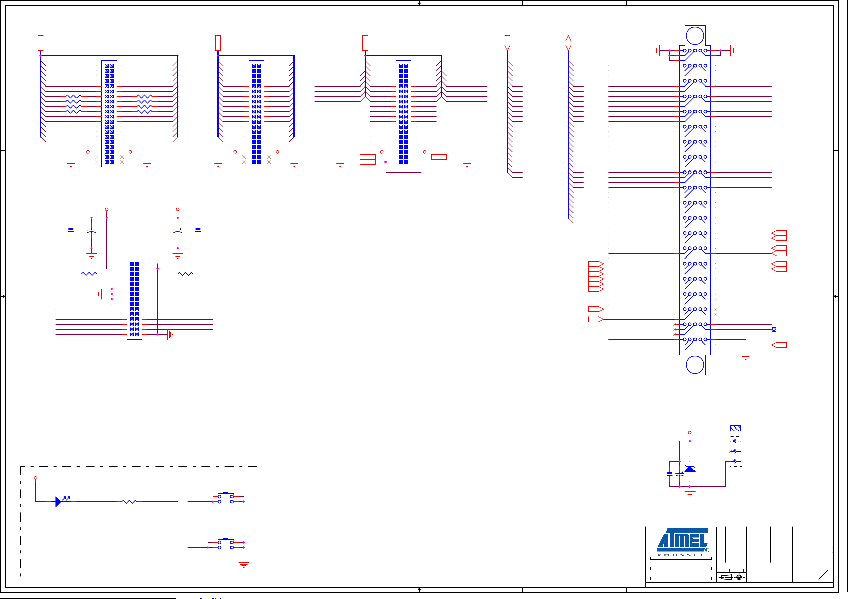
8
J23J23
PA1
PA3
PA5
D D
RR8-2 0RRR8-2 0R
RR8-4 0RRR8-4 0R
RR7-2 0RRR7-2 0R
RR7-4 0RRR7-4 0R
PA7
PA9
PA11
PA13
PA15
PA17
PA19
PA21
PA23
PA25
PA27
PA29
PA31
2 7
4 5
2 7
4 5
1 2
3 4
5 6
7 8
9 10
11 12
13
14
15
16
17
18
19
20
21 22
23 24
25 26
27 28
29 30
31 32
33 34
35 36
3V3 3V3 3V33V3 3V3 3V 3
37 38
39 40
PIO A PIO B PIO C & ADC
C131
C131
10V
10V
10µF
10µF
R108 0RR108 0R
1V0
J28J28
1 2
3 4
5 6
7 8
9 10
11 12
13
15
17
19
21 22
23 24
25 26
27 28
29 30
C130
C130
100NF
100NF
C C
PIO_CNTRL1
TWCK
ISI_DATA[1]
ISI_DATA[3]
ISI_DATA[5]
ISI_DATA[7]
ISI_DATA[9]
ISI_DATA[11]
PC4
PA24
PB21
PB23
PB25
PB27
PB11
PB13
IMAGE SENSOR CONNECTOR
7
PA0
PA2
PA4
PA6
PA8
PA10
18
PA12
RR8-1 0RRR8-1 0R
36
PA14
RR8-3 0RRR8-3 0R
18
PA16
RR7-1 0RRR7-1 0R
36
PA18
RR7-3 0RRR7-3 0R
PA20
PA22
PA24
PA26
PA28
PA30
3V3
C133
C133
100NF
100NF
C132
C132
10V
10V
10µF
10µF
R109 0RR109 0R
14
16
18
20
PB19
PA23
PB31
PB29
PB30
PB28
PB20
PB22
PB24
PB26
PB10
PB12
PB1
PB3
PB5
PB7
PB9
PB11
PB13
PB15
PB17
PB19
PB21
PB23
PB25
PB27
PB29
PB31
PIO_CNTRL2
TWD
ISI_MCK
ISI_VSYNC
ISI_HSYNC
ISI_PCK
ISI_DATA[0]
ISI_DATA[2]
ISI_DATA[4]
ISI_DATA[6]
ISI_DATA[8]
ISI_DATA[10]
6
J26J26
1 2
3 4
5 6
7 8
9 10
11 12
13
15
17
19
21 22
23 24
25 26
27 28
29 30
31 32
33 34
35 36
37 38
39 40
5
J24J24
1 2
PC11
PC15
AVDD
AGND
PC1
PC3
PC5
PC7
PC9
PC11
PC13
PC15
D17
D19
D21
D23
D25
D27
D29
D31
3 4
5 6
7 8
9 10
11 12
13
15
17
19
21 22
23 24
25 26
27 28
29 30
31 32
33 34
35 36
37 38
39 40
PB0
PB2
PB4
PB6
PB8
PB10
14
PB12
16
PB14
18
PB16
20
PB18
PB20
PB22
PB24
PB26
PB28
PB30
A24
CFCE2
CFCS1_NCS5
NCS2
NCS6
NWAIT
PC0
PC2
PC4
PC6
PC8
PC10
14
PC12
16
PC14
18
D16
20
D18
D20
D22
D24
D26
D28
D30
PC4PC5
PC6PC7
PC8PC9
PC10
PC12PC13
PC14
VREFP
4
A23
CFCE1
CFCS0_NCS4
A25_CFRNW
NCS7
NANDCS_NCS3
A0
NBS0_A0
NWR2_NBS2 _A1
A1
A2
A3
A4
A5
A6
A7
A8
A9
A10
A11
A12
A13
A14
A15
A16
A17
A18
A19
A20
A21
A22
3
D[0..31]A[0..22]PC[0..15]PB[0..31]PA[0..31]
D0
D1
D2
D3
D4
D5
D6
D7
D8
D9
D10
D11
D12
D13
D14
D15
D16
D17
D18
D19
D20
D21
D22
D23
D24
D25
D26
D27
D28
D29
D30
D31
CFIOW_ NBS3_NWR 3
CFOE_NR D
SDWE
SDCKE
CAS
RAS
NANDOE
NANDW E
SPARE2
D0
D1
D2
D5
D6
D7
D10
D11
D12
D15
D16
D17
D20
D21
D22
D25
D26
D27
D30
D31
A0
A3
A4
A5
A8
A9
A10
A13
A14
A15
A18
A19
A20
PC4
PC5
PC10
PC11
PC14
PC8
PC9
PC7
PC12
PB19
PB20
PB21
NBS0_A0
A23
A24
A25_CFRNW
NCS2
NANDCS_NCS3
CFCS0_NCS4
CFCS1_NCS5
CFCE2
NCS7
2
J25
J25
Interposer 100 TOP
Interposer 100 TOP
A1
B1
C1
A2
B2
C2
A3
B3
C3
A4
B4
C4
A5
B5
C5
A6
B6
C6
A7
B7
C7
A8
B8
C8
A9
B9
C9
A10
B10
C10
A11
B11
C11
A12
B12
C12
A13
B13
C13
A14
B14
C14
A15
B15
C15
A16
B16
C16
A17
B17
C17
A18
B18
C18
A19
B19
C19
A20
B20
C20
E1
D1
E2
D2
E3
D3
E4
D4
E5
D5
E6
D6
E7
D7
E8
D8
E9
D9
E10
D10
E11
D11
E12
D12
E13
D13
E14
D14
E15
D15
E16
D16
E17
D17
E18
D18
E19
D19
E20
D20
D4
D3
D9
D8
D14
D13
D19
D18
D24
D23
D29
D28
A2
NWR2_NBS2 _A1
A1
A7
A6
A12
A11
A17
A16
A22
A21
PC13
PC15
PC6
PB30
NCS6
NWAIT
CFCE1
1
SDCS_NC S1
NCS0
CFW E_NWE_NW R0
CFIOR_NBS 1_NWR1
SDA10
SDCK
SPARE1
SPARE0
NRST
B B
EBI CONNECTORS
NOT POPULATED
3V3
C134
C134
47 uF
47 uF
6V3
6V3
CR2
USER INTERFACE
3V3
GREEN
GREEN
DS5
A A
DS5
8
R118 220RR1 18 220R
PB8
PA30
PA31
7
BP3BP3
BP4BP4
6
5
4
3
C135
C135
100NF
100NF
AT91SAM9G20-EK
AT91SAM9G20-EK
AT91SAM9G20-EK
CR2
3.3V
3.3V
EXPANSION _UI
EXPANSION _UI
EXPANSION _UI
This agreement is our property. Reproduction and publication without our written authorization shall expose offender to legal proceedings.
This agreement is our property. Reproduction and publication without our written authorization shall expose offender to legal proceedings.
This agreement is our property. Reproduction and publication without our written authorization shall expose offender to legal proceedings.
2
Z15Z15
J31-1J31-1
J31-2J31-2
J31-3J31-3
NOT POPULATED
D
D
D
INIT EDIT
INIT EDIT
INIT EDIT
A
A
A
REV
REV
REV
SCALE
SCALE
SCALE
1/1
1/1
1/1
PP
PP
PP
TVT
TVT
TVT
DES.
DES.
DES.
06/03/09
06/03/09
06/03/09
07/10/08PPC
07/10/08PPC
07/10/08PPC
02/07/08B PP
02/07/08B PP
02/07/08B PP
15/04/08
15/04/08
15/04/08
DATE
DATE
DATE
1
DATEMODIF.
VER.
DATEMODIF.
VER.
DATEMODIF.
VER.
REV. SHEET
REV. SHEET
REV. SHEET
7
7
7
D
D
D
7
7
7

6.1 Wrong Silkscreen of BB and 1.0V on the Board
There is a silkscreen reversion on the board, for the selection of the VDDBU source:
On J10 position 1-2, the marking should be ‘BB’ for Battery Backup instead of ‘1.0V’
On J10 position 2-3, the marking should be ‘1.0V’ instead of ‘BB’.
This erratum is not applicable for AT91SAM9G20-EK Rev. C and later versions.
6.2 Choice of an Oscillator Capacitance
For many reasons at the manufacturing level, Atmel does not specify any crystal references at the board
design stage.
Because of that, the user can find an inconsistency in the value of the used capacitance of the
18.432 MHz crystal on each pin (C23, C24), and the nominal load capacitance of the crystal.
As a reminder, here is the way to select these values.The electrical parameter allows you to fit the right
values provided by the crystal manufacturer - and not by Atmel. They are called "Load Capacitance" of
the crystal. You have to take stray capacitances (package, socket, trace) into account in order to be
close enough to the equivalent nominal Load Capacitance.
Section 6
Errata
With the on-board HCM49-18.432MABJT crystal reference, 10 pF capacitances have been fitted on the
18.432 MHz crystal for a nominal 27 pF load capacitance.
6.3 SD Card Slots and Booting Capability
On the board, Slot J13 is incorrectly marked with a “bootable” mention (solder side). This should be
applied to J35 instead. However, the schematic entitled ” Memory” attached to this User Guide, in Sec-
tion 5.1 ”Schematics” does represent the correct location and marking.
AT91SAM9G20-EK Evaluation Board User Guide 6-1
6413C–ATARM–18-Feb-09

Errata
6-2 AT91SAM9G20-EK Evaluation Board User Guide
6413C–ATARM–18-Feb-09

7.1 Revision History
Table 7-1.
Document Comments
6413C
6413B Errata section created with
Section 6.3 ”SD Card Slots and Booting Capability”, added to errata 6874
Section 6.2 ”Choice of an Oscillator Capacitance” added to errata 6392
New schematics pdf file (at91sam9g20-ek revc.pdf) attached to
Section 1.2 ”Deliverables” on page 1-1, last bullet added
-
Section 3.8 ”Power Supply Circuitry” on page 3-5, last bullet added
-
- PA23-24 rows edited in
- 2 rows (J33-34) added to Table 4-1 on page 4-1
Section 7
Revision History
Section 6.1 ”Wrong Silkscreen of BB and 1.0V on the Board” 5413
Section 5.1 ”Schematics” 5936
Table 3-1 on page 3-7
Change
Request
Ref
5851
- Section 1.3 ”AT91SAM9G20-EK Evaluation Board” on page 1-1: ‘one’ DataFlash changed to ‘two’
- 3 figures changed: Figure 2-1 on page 2-2, Figure 2-2 on page 2-3, and Figure 2-3 on page 2-5
- Typo in Section 2.6 ”Getting Started” on page 2-4: ‘tools’ instead of ‘tool’
- 4 bullets removed from
- 2 bullets edited in Section 3.13 ”Expansion Slot” on page 3-6
- PA6 to PA11 rows edited in Table 3-1 on page 3-7
- PB0 and PB8-9 rows edited in Table 3-2 on page 3-8
- A paragraph added at the end of Section 4.5 ”Ethernet” on page 4-3
6413A First Issue
Section 3.11 ”User Interface” on page 3-6
RFO
AT91SAM9G20-EK Evaluation Board User Guide 7-1
6413C–ATARM–18-Feb-09

Revision History
7-2 AT91SAM9G20-EK Evaluation Board User Guide
6413C–ATARM–18-Feb-09

Headquarters International
Atmel Corporation
2325 Orchard Parkway
San Jose, CA 95131
USA
Tel: 1(408) 441-0311
Fax: 1(408) 487-2600
Atmel Asia
Unit 1-5 & 16, 19/F
BEA Tower, Millennium City 5
418 Kwun Tong Road
Kwun Tong, Kowloon
Hong Kong
Tel: (852) 2245-6100
Fax: (852) 2722-1369
Product Contact
Web Site
www.atmel.com
www.atmel.com/AT91SAM
Literature Requests
www.atmel.com/literature
Atmel Europe
Le Krebs
8, Rue Jean-Pierre Timbaud
BP 309
78054 Saint-Quentin-enYvelines Cedex
France
Tel: (33) 1-30-60-70-00
Fax: (33) 1-30-60-71-11
Technical Support
AT91SAM Support
Atmel techincal support
Atmel Japan
9F, Tonetsu Shinkawa Bldg.
1-24-8 Shinkawa
Chuo-ku, Tokyo 104-0033
Japan
Tel: (81) 3-3523-3551
Fax: (81) 3-3523-7581
Sales Contacts
www.atmel.com/contacts/
Disclaimer: The information in this document is provided in connection with Atmel products. No license, express or implied, by estoppel or otherwise, to any
intellectual property right is granted by this document or in connection with the sale of Atmel products. EXCEPT AS SET FORTH IN ATMEL’S TERMS AND CONDI-
TIONS OF SALE LOCATED ON ATMEL’S WEB SITE, ATMEL ASSUMES NO LIABILITY WHATSOEVER AND DISCLAIMS ANY EXPRESS, IMPLIED OR STATUTORY
WARRANTY RELATING TO ITS PRODUCTS INCLUDING, BUT NOT LIMITED TO, THE IMPLIED WARRANTY OF MERCHANTABILITY, FITNESS FOR A PARTICULAR
PURPOSE, OR NON-INFRINGEMENT. IN NO EVENT SHALL ATMEL BE LIABLE FOR ANY DIRECT, INDIRECT, CONSEQUENTIAL, PUNITIVE, SPECIAL OR INCIDENTAL DAMAGES (INCLUDING, WITHOUT LIMITATION, DAMAGES FOR LOSS OF PROFITS, BUSINESS INTERRUPTION, OR LOSS OF INFORMATION) ARISING OUT OF
THE USE OR INABILITY TO USE THIS DOCUMENT, EVEN IF ATMEL HAS BEEN ADVISED OF THE POSSIBILITY OF SUCH DAMAGES. Atmel makes no
representations or warranties with respect to the accuracy or completeness of the contents of this document and reserves the right to make changes to specifications
and product descriptions at any time without notice. Atmel does not make any commitment to update the information contained herein. Unless specifically provided
otherwise, Atmel products are not suitable for, and shall not be used in, automotive applications. Atmel’s products are not intended, authorized, or warranted for use
as components in applications intended to support or sustain life.
© 2009 Atmel Corporation. All rights reserved. Atmel®, logo and combinations thereof, DataFlash® and others are registered trademarks or
trademarks of Atmel Corporation or its subsidiaries. ARM
®
, Thumb®, the ARMPowered® logo and others are registered trademarks or trade-
marks of ARM Ltd. Other terms and product names may be trademarks of others.
6413C–ATARM–18-Feb-09
 Loading...