


AT91SAM7X-EK
Evaluation Board
for AT91SAM7X and AT91SAM7XC
..............................................................................................
User Guide

2 AT91SAM7X-EK Evaluation Board User Guide
6195E–ATARM–22-Mar-07

Table of Contents
Section 1
Overview...............................................................................................1-1
1.1 Scope........................................................................................................1-1
1.2 Deliverables ..............................................................................................1-1
1.3 The AT91SAM7X-EK Evaluation Board....................................................1-1
Section 2
Setting Up the AT91SAM7X-EK
Evaluation Board ..................................................................................2-1
2.1 Electrostatic Warning ................................................................................2-1
2.2 Requirements............................................................................................2-1
2.3 Layout .......................................................................................................2-2
2.4 Powering Up the Board.............................................................................2-3
2.5 Getting Started..........................................................................................2-3
2.6 AT91SAM7X-EK Block Diagram ...............................................................2-4
Section 3
Board Description ................................................................................. 3-1
3.1 AT91SAM7X Microcontroller.....................................................................3-1
3.2 AT91SAM7X Block Diagram .....................................................................3-4
3.3 AT91SAM7XC Microcontroller ..................................................................3-5
3.4 AT91SAM7XC Export Regulations Statement..........................................3-7
3.5 AT91SAM7XC Block Diagram ..................................................................3-8
3.6 Memory .....................................................................................................3-9
3.7 Clock Circuitry...........................................................................................3-9
3.8 Reset Circuitry ..........................................................................................3-9
3.9 Power Supply Circuitry..............................................................................3-9
3.10 Remote Communication ...........................................................................3-9
3.11 Analog Interface........................................................................................3-9
3.12 User Interface ...........................................................................................3-9
3.13 Debug Interface ......................................................................................3-10
3.14 Expansion Slot ........................................................................................3-10
Section 4
Configuration Straps .............................................................................4-1
4.1 Configuration Straps .................................................................................4-1
Section 5
Schematics ........................................................................................... 5-1
5.1 Schematics ...............................................................................................5-1
AT91SAM7X-EK Evaluation Board User Guide i
6195E–ATARM–22-Mar-076195E–ATARM–22-Mar-07

Section 6
Errata....................................................................................................6-1
6.1 Errata ........................................................................................................6-1
Section 7
Revision History....................................................................................7-1
7.1 Revision History ........................................................................................7-1
ii AT91SAM7X-EK Evaluation Board User Guide
6195E–ATARM–22-Mar-07

Section 1
Overview
1.1 Scope The AT91SAM7X-EK and the AT91SAM7XC-EK evaluation kits enable evaluation capa-
bilities and code development of applications running on the AT91SAM7X or the
AT91SAM7XC microcontroller.
This guide focuses on the AT91SAM7X-EK board as a common evaluation platform for
the AT91SAM7X and AT91SAM7XC devices in a 100-lead LQFP package.
1.2 Deliverables The package contains the following items:
! a board marked AT91SAM7X-EK
! one A/B-type USB cable
! one crossed serial RS232 cable
! one RJ45 crossed Ethernet cable
1.3 The AT91SAM7XEK Evaluation
Board
! universal input AC/DC power supply with US and EU plug adapter
! one DVD-ROM containing summary and full datasheets, datasheets with electrical
and mechanical characteristics, application notes and getting started documents for
all development boards and AT91 microcontrollers. An AT91 software package with C
and assembly listings is also provided. This allows the user to begin evaluating the
AT91 A R M
Depending on the model of the kit, the board is equipped with either an AT91SAM7X256
or an AT91SAM7XC256 (100-pin LQFP Green package) together with the following
interfaces:
! USB device port
! DBGU serial communication port
! RS232 serial communication port with RTS/CTS
! JTAG/ICE debug interface connector
! serial CAN communication ports
! MII Ethernet 100-base TX with auto MDIX capability
! buffered analog input and PWM output
®
Thumb® 32-bit microcontroller quickly.
AT91SAM7X-EK Evaluation Board User Guide 1-1
6195E–ATARM–22-Mar-07

Overview
! Power LED and general-purpose LEDs
! DataFlash
®
card slot
! expansion connector
! Atmel
®
serial DataFlash
! One footprint for Atmel Serial EEPROM (MN11)
1-2 AT91SAM7X-EK Evaluation Board User Guide
6195E–ATARM–22-Mar-07

Section 2
Setting Up the AT91SAM7X-EK
Evaluation Board
2.1 Electrostatic Warning
The AT91SAM7X-EK evaluation board is shipped in a protective anti-static package.
The board must not be subjected to high electrostatic potentials. A grounding strap or
similar protective device should be worn when handling the board. Avoid touching the
component pins or any other metallic element.
2.2 Requirements In order to set up the AT91SAM7X-EK evaluation board, the following items are
required:
! the AT91SAM7X-EK evaluation board itself
! an A/B-type USB cable
or
! a DC USB power adapter (5V at 0.5 A) with USB A/B cable
Note: The kit is not delivered with a JTAG/ICE interface which is required to start eval-
uating the device.
AT91SAM7X-EK Evaluation Board User Guide 2-1
6195E–ATARM–22-Mar-07
Setting Up the AT91SAM7X-EK Evaluation Board
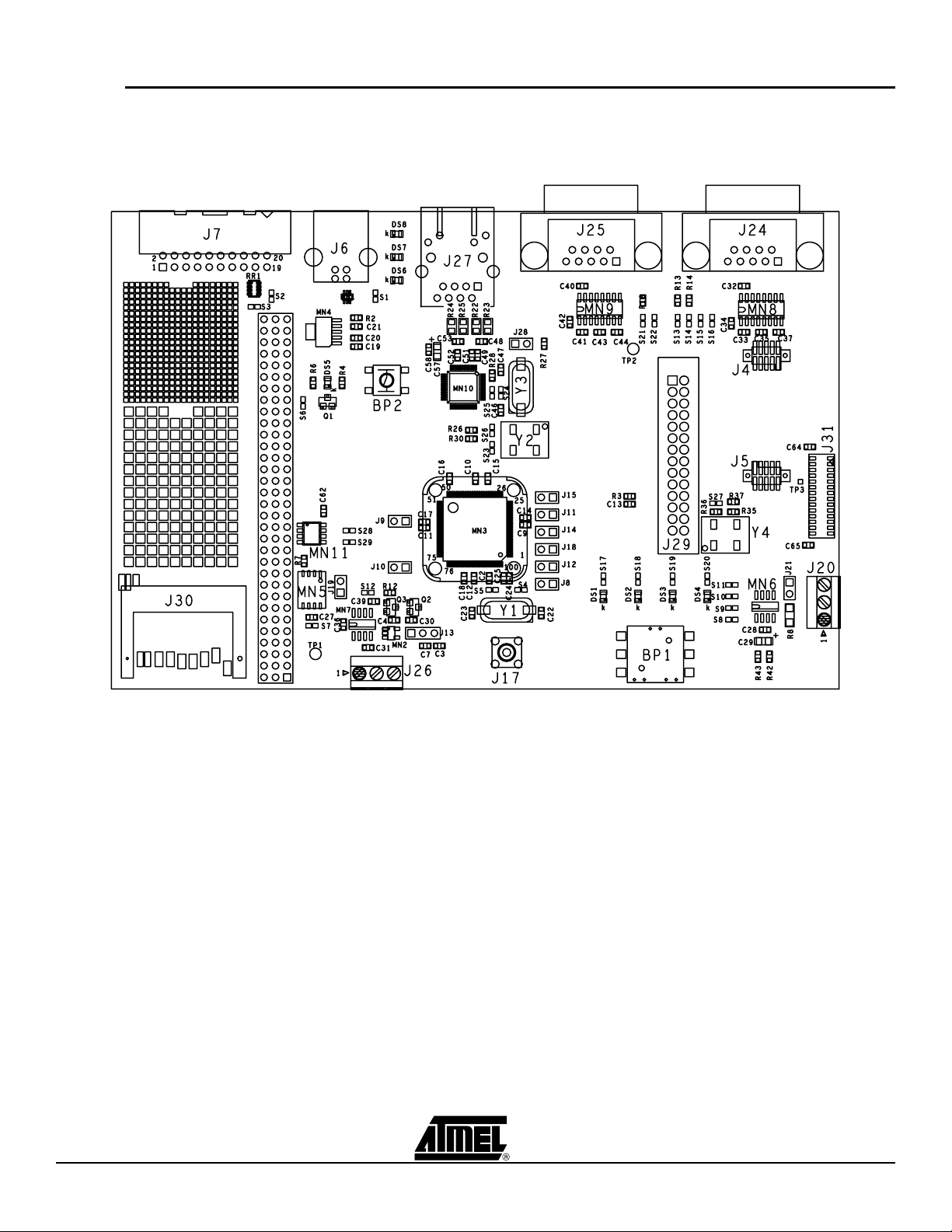
2.3 Layout
Figure 2-1. Layout - Top View
2-2 AT91SAM7X-EK Evaluation Board User Guide
6195E–ATARM–22-Mar-07
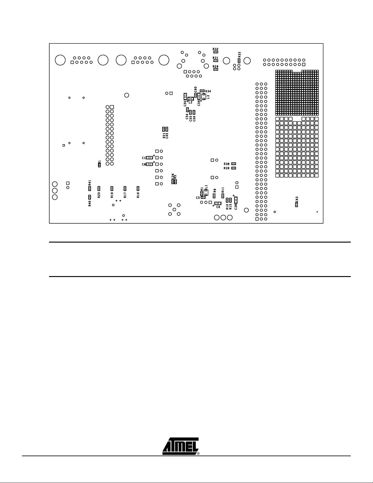
Figure 2-2. Layout - Bottom View
Setting Up the AT91SAM7X-EK Evaluation Board
2.4 Powering Up the
The AT91SAM7X-EK board is self-powered by the USB port or by a USB power adapter.
Board
2.5 Getting Started The AT91SAM7X-EK evaluation board is delivered with a DVD-ROM containing all nec-
essary information and step-by-step procedures for working with the most common
development tool chains. Please refer to this DVD-ROM, or to the AT91 web site,
http://www.atmel.com/products/AT91/, for the most up-to-date information on getting
started with the evaluation kit.
AT91SAM7X-EK Evaluation Board User Guide 2-3
6195E–ATARM–22-Mar-07
Setting Up the AT91SAM7X-EK Evaluation Board
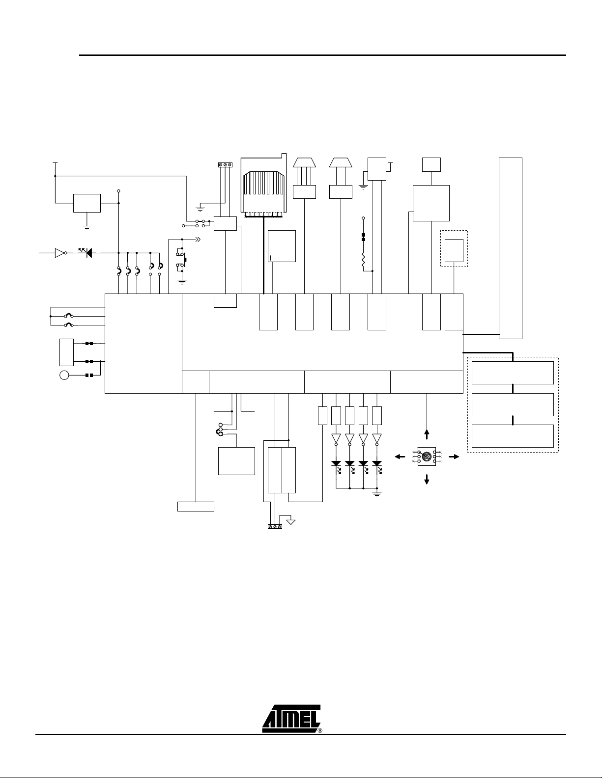
2.6 AT91SAM7X-EK Block Diagram
Figure 2-3. Block Diagram
VBUS
IN OUT
YELLOWYELLOW
PIO
LIGHTED WHEN POWER ON
18.432 MHz
EXT CLK INPUT
3V3
POWER LED
VDDOUT
VDDCORE
VDDPLL
3V3
VDDIN
SYSTEM CONTROLLER
XOUT
XIN
VDDIO
VDDFLASH
ERASE
TST
5V
3V3
NRST
MANUAL RESET
NRST
JTAG/ICE
JTAG/ICE CONNECTOR
DATAFLASH CARD READER
CANL1CANH
RS
CAN
VDDANA
ADVREFP
3.3VANA
3
2
1
J7J7
3.00V +- 0.2%
EXTERNAL REF
8 57 6 4 3 2 1 9
SPI0_NPCS1
PIO
ADC
GNDANA
GNDANA
1
ANALOG INPUT
RS232
TXD
CTS
RTS
RXD
SERIAL
DATAFLASH
CS
SPI0_NPCS0
SPI0
RXD - TXD - RTS - CTS
USART0
AT91SAM7X256
AT91SAM7XC256
(LQFP100)
AD4
AD5
0 TO VREF
0 TO VREF
EXTERNAL INPUT
PWM VOLTAGE GEN.
DBGU
RS232
TXD
DRXD - DTXD
PB19
PB30
PWM0
PWM3
USER'S GREEN LED
RXD
DBGU
PB20
PWM1
USB DEVICE
3V3
1K51K5
PIO
PB21
PWM2
DDP
VBUS
DDM
USB
PB22
PWM3
ETHERNET 10/100
MDI/MDIX AUTO CROSSOVER
RJ45
ETHERNET PHY
PWD
NOT POPULATED
Serial
EEprom
MII INTERFACE
SCL - SDA
PIO
EMAC
PIO APWM0..PWM3PIO B
1
4
52
3 6
USER'S TACT SWITCH
PIO A - PIO B EXPANSION CONNECTOR
TWI
PIO A
PIO B
NOT POPULATED
RF CONNECTORS
ZIGBEE AT86RF210 MODULE
RF CONNECTORS
AT86RF230 MODULE
RF CONNECTORS
ATR2406 MODULE
2-4 AT91SAM7X-EK Evaluation Board User Guide
6195E–ATARM–22-Mar-07

Section 3
Board Description
3.1 AT91SAM7X Microcontroller
! Incorporates the ARM7TDMI® ARM® Thumb® Processor
– High-performance 32-bit RISC Architecture
– High-density 16-bit Instruction Set
– Leader in MIPS/Watt
– EmbeddedICE
! Internal High-speed Flash
– 256 Kbytes (AT91SAM7X256) Organized in 1024 Pages of 256 Bytes
– 128 Kbytes (AT91SAM7X128) Organized in 512 Pages of 256 Bytes
– Single Cycle Access at Up to 30 MHz in Worst Case Conditions
– Prefetch Buffer Optimizing Thumb Instruction Execution at Maximum Speed
– Page Programming Time: 6 ms, Including Page Auto-erase,
Full Erase Time: 15 ms
– 10,000 Write Cycles, 10-year Data Retention Capability,
Sector Lock Capabilities, Flash Security Bit
– Fast Flash Programming Interface for High Volume Production
! Internal High-speed SRAM, Single-cycle Access at Maximum Speed
– 64 Kbytes (AT91SAM7X256)
– 32 Kbytes (AT91SAM7X128)
! Memory Controller (MC)
– Embedded Flash Controller, Abort Status and Misalignment Detection
™
, Debug Communication Channel Support
! Reset Controller (RSTC)
– Based on Power-on Reset Cells and Low-power Factory-calibrated Brownout
Detector
– Provides External Reset Signal Shaping and Reset Source Status
! Clock Generator (CKGR)
– Low-power RC Oscillator, 3 to 20 MHz On-chip Oscillator and one PLL
! Power Management Controller (PMC)
AT91SAM7X-EK Evaluation Board User Guide 3-1
6195E–ATARM–22-Mar-07

Board Description
– Power Optimization Capabilities, Including Slow Clock Mode (Down to 500 Hz)
and Idle Mode
– Four Programmable External Clock Signals
! Advanced Interrupt Controller (AIC)
– Individually Maskable, Eight-level Priority, Vectored Interrupt Sources
– Two External Interrupt Sources and One Fast Interrupt Source, Spurious
Interrupt Protected
! Debug Unit (DBGU)
– 2-wire UART and Support for Debug Communication Channel interrupt,
Programmable ICE Access Prevention
! Periodic Interval Timer (PIT)
– 20-bit Programmable Counter plus 12-bit Interval Counter
! Windowed Watchdog (WDT)
– 12-bit key-protected Programmable Counter
– Provides Reset or Interrupt Signals to the System
– Counter May Be Stopped While the Processor is in Debug State or in Idle
Mode
! Real-time Timer (RTT)
– 32-bit Free-running Counter with Alarm
– Runs Off the Internal RC Oscillator
! Two Parallel Input/Output Controllers (PIO)
– Sixty-two Programmable I/O Lines Multiplexed with up to Two Peripheral I/Os
– Input Change Interrupt Capability on Each I/O Line
– Individually Programmable Open-drain, Pull-up Resistor and Synchronous
Output
! Thirteen Peripheral DMA Controller (PDC) Channels
! One USB 2.0 Full Speed (12 Mbits per second) Device Port
– On-chip Transceiver, 1352-byte Configurable Integrated FIFOs
! One Ethernet MAC 10/100 base-T
– Media Independent Interface (MII) or Reduced Media Independent Interface
(RMII)
– Integrated 28-byte FIFOs and Dedicated DMA Channels for Transmit and
Receive
! One Part 2.0A and Part 2.0B Compliant CAN Controller
– Eight Fully-programmable Message Object Mailboxes, 16-bit Time Stamp
Counter
! One Synchronous Serial Controller (SSC)
– Independent Clock and Frame Sync Signals for Each Receiver and
Transmitter
– I²S Analog Interface Support, Time Division Multiplex Support
– High-speed Continuous Data Stream Capabilities with 32-bit Data Transfer
3-2 AT91SAM7X-EK Evaluation Board User Guide
6195E–ATARM–22-Mar-07

Board Description
! Two Universal Synchronous/Asynchronous Receiver Transmitters (USART)
– Individual Baud Rate Generator, IrDA
®
Infrared Modulation/Demodulation
– Support for ISO7816 T0/T1 Smart Card, Hardware Handshaking, RS485
Support
– Full Modem Line Support on USART1
! Two Master/Slave Serial Peripheral Interfaces (SPI)
– 8- to 16-bit Programmable Data Length, Four External Peripheral Chip Selects
! One Three-channel 16-bit Timer/Counter (TC)
– Three External Clock Inputs, Two Multi-purpose I/O Pins per Channel
– Double PWM Generation, Capture/Waveform Mode, Up/Down Capability
! One Four-channel 16-bit Power Width Modulation Controller (PWMC)
! One Two-wire Interface (TWI)
– Master Mode Support Only, All Two-wire Atmel EEPROMs Supported
! One 8-channel 10-bit Analog-to-Digital Converter, Four Channels Multiplexed with
Digital I/Os
! SAM-BA
™
Boot Assistance
– Default Boot program
– Interface with SAM-BA Graphic User Interface
! IEEE
®
1149.1 JTAG Boundary Scan on All Digital Pins
! 5V-tolerant I/Os, Including Four High-current Drive I/O lines, Up to 16 mA Each
! Power Supplies
– Embedded 1.8V Regulator, Drawing up to 100 mA for the Core and External
Components
– 3.3V VDDIO I/O Lines Power Supply, Independent 3.3V VDDFLASH Flash
Power Supply
– 1.8V VDDCORE Core Power Supply with Brownout Detector
! Fully Static Operation: Up to 55 MHz at 1.65V and 85°C Worst Case Conditions
! Available in a 100-lead LQFP Green Package
AT91SAM7X-EK Evaluation Board User Guide 3-3
6195E–ATARM–22-Mar-07

Board Description
3.2 AT91SAM7X Block Diagram
Figure 3-1. Block Diagram
TDI
TDO
TMS
TCK
JTAGSEL
TST
FIQ
IRQ0-IRQ1
DRXD
DTXD
PCK0-PCK3
PLLRC
XIN
XOUT
VDDCORE
VDDFLASH
VDDCORE
NRST
RXD0
TXD0
SCK0
RTS0
CTS0
RXD1
TXD1
SCK1
RTS1
CTS1
DCD1
DSR1
DTR1
RI1
SPI0_NPCS0
SPI0_NPCS1
SPI0_NPCS2
SPI0_NPCS3
SPI0_MISO
SPI0_MOSI
SPI0_SPCK
SPI1_NPCS0
SPI1_NPCS1
SPI1_NPCS2
SPI1_NPCS3
SPI1_MISO
SPI1_MOSI
SPI1_SPCK
ADTRG
AD0
AD1
AD2
AD3
AD4
AD5
AD6
AD7
ADVREF
System Controller
PIO
PLL
OSC
RCOSC
BOD
POR
PIOA
PIO
JTAG
SCAN
DBGU
Controller
AIC
PMC
Reset
PIT
WDT
RTT
PIOB
PDC
PDC
ICE
USART0
USART1
SPI0
SPI1
ADC
ARM7TDMI
Processor
Memory Controller
Embedded
Flash
Controller
Abort
Status
Peripheral Bridge
Peripheral DMA
Controller
13 Channels
APB
PDC
PDC
PDC
PDC
PDC
PDC
PDC
PDC
PDC
Address
Decoder
Misalignment
Detection
DMA
FIFO
Ethernet MAC 10/100
FIFO
PDC
PDC
USB Device
PWMC
SSC
Timer Counter
TC0
TC1
TC2
TWI
CAN
1.8 V
Voltage
Regulator
SRAM
64/32 Kbytes
Flash
256/128 Kbytes
ROM
Fast Flash
Programming
Interface
SAM-BA
VDDIN
GND
VDDOUT
VDDCORE
VDDIO
VDDFLASH
ERASE
PGMRDY
PGMNVALID
PGMNOE
PGMCK
PGMM0-PGMM3
PGMD0-PGMD15
PGMNCMD
PGMEN0-PGMEN1
ETXCK-ERXCK-EREFCK
ETXEN-ETXER
ECRS-ECOL, ECRSDV
ERXER-ERXDV
ERX0-ERX3
PIO
ETX0-ETX3
EMDC
EMDIO
EF100
VDDFLASH
DDM
PIO
DDP
PWM0
PWM1
PWM2
PWM3
TF
TK
TD
RD
RK
RF
TCLK0
TCLK1
TCLK2
TIOA0
TIOB0
TIOA1
TIOB1
TIOA2
TIOB2
TWD
TWCK
CANRX
CANTX
Transceiver
3-4 AT91SAM7X-EK Evaluation Board User Guide
6195E–ATARM–22-Mar-07

Board Description
3.3 AT91SAM7XC Microcontroller
! Incorporates the ARM7TDMI® ARM® Thumb® Processor
– High-performance 32-bit RISC Architecture
– High-density 16-bit Instruction Set
– Leader in MIPS/Watt
– EmbeddedICE
™
, Debug Communication Channel Support
! Internal High-speed Flash
– 256 Kbytes (AT91SAM7XC256) Organized in 1024 Pages of 256 Bytes
– 128 Kbytes (AT91SAM7XC128) Organized in 512 Pages of 256 Bytes
– Single Cycle Access at Up to 30 MHz in Worst Case Conditions
– Prefetch Buffer Optimizing Thumb Instruction Execution at Maximum Speed
– Page Programming Time: 6 ms, Including Page Auto-erase,
Full Erase Time: 15 ms
– 10,000 Write Cycles, 10-year Data Retention Capability,
Sector Lock Capabilities, Flash Security Bit
– Fast Flash Programming Interface for High Volume Production
! Internal High-speed SRAM, Single-cycle Access at Maximum Speed
– 64 Kbytes (AT91SAM7XC256)
– 32 Kbytes (AT91SAM7XC128)
! Memory Controller (MC)
– Embedded Flash Controller, Abort Status and Misalignment Detection
! Reset Controller (RSTC)
– Based on Power-on Reset Cells and Low-power Factory-calibrated Brownout
Detector
– Provides External Reset Signal Shaping and Reset Source Status
! Clock Generator (CKGR)
– Low-power RC Oscillator, 3 to 20 MHz On-chip Oscillator and one PLL
! Power Management Controller (PMC)
– Power Optimization Capabilities, Including Slow Clock Mode (Down to 500 Hz)
and Idle Mode
– Four Programmable External Clock Signals
! Advanced Interrupt Controller (AIC)
– Individually Maskable, Eight-level Priority, Vectored Interrupt Sources
– Two External Interrupt Sources and One Fast Interrupt Source, Spurious
Interrupt Protected
! Debug Unit (DBGU)
– 2-wire UART and Support for Debug Communication Channel interrupt,
Programmable ICE Access Prevention
! Periodic Interval Timer (PIT)
– 20-bit Programmable Counter plus 12-bit Interval Counter
! Windowed Watchdog (WDT)
AT91SAM7X-EK Evaluation Board User Guide 3-5
6195E–ATARM–22-Mar-07

Board Description
– 12-bit key-protected Programmable Counter
– Provides Reset or Interrupt Signals to the System
– Counter May Be Stopped While the Processor is in Debug State or in Idle
Mode
! Real-time Timer (RTT)
– 32-bit Free-running Counter with Alarm
– Runs Off the Internal RC Oscillator
! Two Parallel Input/Output Controllers (PIO)
– Sixty-two Programmable I/O Lines Multiplexed with up to Two Peripheral I/Os
– Input Change Interrupt Capability on Each I/O Line
– Individually Programmable Open-drain, Pull-up Resistor and Synchronous
Output
! Seventeen Peripheral DMA Controller (PDC) Channels
! One Advanced Encryption System (AES)
– 128-bit Key Algorithm, Compliant with FIPS PUB 197 Specifications
– Buffer Encryption/Decryption Capabilities with PDC
! One Triple Data Encryption System (TDES)
– Two-key or Three-key Algorithms, Compliant with FIPS PUB 46-3
Specifications
– Optimized for Triple Data Encryption Capability
! One USB 2.0 Full Speed (12 Mbits per second) Device Port
– On-chip Transceiver, 1352-byte Configurable Integrated FIFOs
! One Ethernet MAC 10/100 base-T
– Media Independent Interface (MII) or Reduced Media Independent Interface
(RMII)
– Integrated 28-byte FIFOs and Dedicated DMA Channels for Transmit and
Receive
! One Part 2.0A and Part 2.0B Compliant CAN Controller
– Eight Fully-programmable Message Object Mailboxes, 16-bit Time Stamp
Counter
! One Synchronous Serial Controller (SSC)
– Independent Clock and Frame Sync Signals for Each Receiver and
Transmitter
– I²S Analog Interface Support, Time Division Multiplex Support
– High-speed Continuous Data Stream Capabilities with 32-bit Data Transfer
! Two Universal Synchronous/Asynchronous Receiver Transmitters (USART)
– Individual Baud Rate Generator, IrDA
®
Infrared Modulation/Demodulation
– Support for ISO7816 T0/T1 Smart Card, Hardware Handshaking, RS485
Support
– Full Modem Line Support on USART1
! Two Master/Slave Serial Peripheral Interfaces (SPI)
3-6 AT91SAM7X-EK Evaluation Board User Guide
6195E–ATARM–22-Mar-07

Board Description
– 8- to 16-bit Programmable Data Length, Four External Peripheral Chip Selects
! One Three-channel 16-bit Timer/Counter (TC)
– Three External Clock Inputs, Two Multi-purpose I/O Pins per Channel
– Double PWM Generation, Capture/Waveform Mode, Up/Down Capability
! One Four-channel 16-bit Power Width Modulation Controller (PWMC)
! One Two-wire Interface (TWI)
– Master Mode Support Only, All Two-wire Atmel EEPROMs Supported
! One 8-channel 10-bit Analog-to-Digital Converter, Four Channels Multiplexed with
Digital I/Os
! SAM-BA
™
Boot Assistance
– Default Boot program
– Interface with SAM-BA Graphic User Interface
! IEEE
®
1149.1 JTAG Boundary Scan on All Digital Pins
! 5V-tolerant I/Os, Including Four High-current Drive I/O lines, Up to 16 mA Each
! Power Supplies
– Embedded 1.8V Regulator, Drawing up to 100 mA for the Core and External
Components
– 3.3V VDDIO I/O Lines Power Supply, Independent 3.3V VDDFLASH Flash
Power Supply
– 1.8V VDDCORE Core Power Supply with Brownout Detector
3.4 AT91SAM7XC Export Regulations Statement
! Fully Static Operation: Up to 55 MHz at 1.65V and 85°C Worst Case Conditions
! Available in a 100-lead LQFP Green Package
These commodities, technology or software will be exported from France and the applicable Export Administration Regulations will apply. French, United States and other
relevant laws, regulations and requirements regarding the export of products may
restrict sale, export and re-export of these products; please assure you conduct your
activities in accordance with the applicable relevant export regulations.
AT91SAM7X-EK Evaluation Board User Guide 3-7
6195E–ATARM–22-Mar-07

Board Description
3.5 AT91SAM7XC Block Diagram
Figure 3-2. Block Diagram
TDI
TDO
TMS
TCK
JTAGSEL
TST
FIQ
IRQ0-IRQ1
DRXD
DTXD
PCK0-PCK3
PLLRC
XIN
XOUT
VDDCORE
VDDFLASH
VDDCORE
NRST
RXD0
TXD0
SCK0
RTS0
CTS0
RXD1
TXD1
SCK1
RTS1
CTS1
DCD1
DSR1
DTR1
SPI0_NPCS0
SPI0_NPCS1
SPI0_NPCS2
SPI0_NPCS3
SPI0_MISO
SPI0_MOSI
SPI0_SPCK
SPI1_NPCS0
SPI1_NPCS1
SPI1_NPCS2
SPI1_NPCS3
SPI1_MISO
SPI1_MOSI
SPI1_SPCK
ADTRG
AD0
AD1
AD2
AD3
AD4
AD5
AD6
AD7
ADVREF
RI1
System Controller
PIO
PLL
OSC
RCOSC
BOD
POR
PIOA
PIO
JTAG
SCAN
DBGU
Controller
AIC
PDC
PDC
PMC
Reset
PIT
WDT
RTT
PIOB
ICE
USART0
USART1
SPI0
SPI1
ADC
ARM7TDMI
Processor
Memory Controller
Embedded
Flash
Controller
Abort
Status
Peripheral Bridge
Peripheral DMA
Controller
17 Channels
APB
PDC
PDC
PDC
PDC
PDC
PDC
PDC
PDC
PDC
Address
Decoder
Misalignment
Detection
DMA
FIFO
Ethernet MAC 10/100
FIFO
PDC
PDC
PDC
PDC
PDC
PDC
USB Device
PWMC
SSC
Timer Counter
TC0
TC1
TC2
TWI
CAN
AES 128
TDES
1.8 V
Voltage
Regulator
SRAM
64/32 Kbytes
Flash
256/128 Kbytes
ROM
Fast Flash
Programming
Interface
SAM-BA
VDDIN
GND
VDDOUT
VDDCORE
VDDIO
VDDFLASH
ERASE
PGMRDY
PGMNVALID
PGMNOE
PGMCK
PGMM0-PGMM3
PGMD0-PGMD15
PGMNCMD
PGMEN0-PGMEN1
ETXCK-ERXCK-EREFCK
ETXEN-ETXER
ECRS-ECOL, ECRSDV
ERXER-ERXDV
ERX0-ERX3
PIO
ETX0-ETX3
EMDC
EMDIO
EF100
VDDFLASH
DDM
PIO
DDP
PWM0
PWM1
PWM2
PWM3
TF
TK
TD
RD
RK
RF
TCLK0
TCLK1
TCLK2
TIOA0
TIOB0
TIOA1
TIOB1
TIOA2
TIOB2
TWD
TWCK
CANRX
CANTX
Transceiver
3-8 AT91SAM7X-EK Evaluation Board User Guide
6195E–ATARM–22-Mar-07

3.6 Memory ! 256 Kbytes of Internal High-speed Flash
! 64 Kbytes of Internal High-speed SRAM
! Atmel serial DataFlash
! One footprint for Atmel Serial EEPROM memory. The user can fit an AT24C128AN or
AT24C256AN or AT24C512AN in 8S1 package as well as a cryptomemory
AT88C25616C-SI
®
3.7 Clock Circuitry ! 18.432 MHz standard crystal for the embedded oscillator
! 32 KHz internal RC oscillator
3.8 Reset Circuitry ! Internal reset controller with a bidirectional reset pin
! External reset pushbutton
Board Description
3.9 Power Supply Circuitry
3.10 Remote Communication
! USB powered, the dynamic power consumption on VDDCORE is less than 90 mA at
full speed when running out of the Flash. The total current at power-up is less than
100 mA.
! External power can be applied via USB Power adapter 5V 0.5A with USB A/B cable
! On-chip embedded VDDCORE 1.8V regulator
! On-board 3.3V 400 mA linear regulator
! One Serial interface (DBGU COM Port) via RS-232 DB9 male socket
! One Serial interface (RS232 COM Port) via RS-232 DB9 male socket
! USB V2.0 Full-speed compliant, 12 Mbits per second (UDP)
! One CAN 2.0B communication port via the 3-position printed circuit terminal block
! One MII Ethernet 100-base TX (auto MDI/MDI-X crossover cable)
3.11 Analog Interface ! One selectable 0.2% 3.00V Vref or 3.3V ANA
! One 3-position printed circuit terminal block
! Two analog up to Vref inputs. One external user input and one back-looped with
buffered PWM3 output.
! One buffered PWM3 analog output (up to Vref)
3.12 User Interface ! One 5-way joystick (4 directions and push for confirmation)
! Four general-purpose buffered green user LEDs (PWM controlled)
AT91SAM7X-EK Evaluation Board User Guide 3-9
6195E–ATARM–22-Mar-07

Board Description
! One yellow power LED (can also be software controlled)
3.13 Debug Interface ! 20-pin JTAG/ICE interface connector
! DBGU serial RS232 COM Port
3.14 Expansion Slot ! One DataFlash card slot
! All I/Os of the AT91SAM7X and the AT91SAM7XC are routed to peripheral extension
connectors (J16). This allows the developer to check the integrity of the components
and to extend the features of the board by adding external hardware components or
boards.
3-10 AT91SAM7X-EK Evaluation Board User Guide
6195E–ATARM–22-Mar-07

4.1 Configuration Straps
Section 4
Configuration Straps
Table 4-1. Configuration Jumpers and Straps
Default
Designation
J8 Opened Erases all internal Flash memory when the board is
J9 Opened Do not use: Factory test mode. J9 is not populated
J10 Opened Selects ICE mode or JTAG mode (Closed). J10 is not
J11 Closed VDDIN Jumper
J12 Closed VDDFLASH Jumper
J13 1-2 ADVREF Jumper select
J14 Closed VDDCORE Jumper
J15 Closed VDDIO Jumper
Setting Feature
powered. To do that, the user will have to close the J8 at
least 200 ms.
populated.
(1)
(1)
1-2: 3.00V Voltage reference
2-3: VDDANA
(1)
(1)
J17 Opened External XIN clock input.
S4 and S5 must be open.
J17 is not populated.
J18 Closed VDDPLL Jumper
J19 Closed Enables the use of the NPCS00 (PA12).
J21 Closed Enables 120 ohms CAN bus resistance termination.
J28 Closed Enables Ethernet Auto MDIX control.
S1 Closed Enables permanent pull up on USB DP.
S2 Closed The System Reset signal (NRST) is connected to the
ICE/JTAG socket (J7, pin 15).
S3 Opened Disables 5V (VUSB) power supply on J16 extension
connector.
AT91SAM7X-EK Evaluation Board User Guide 4-1
(1)
6195E–ATARM–22-Mar-07

Configuration Straps
Table 4-1. Configuration Jumpers and Straps (Continued)
Default
Designation
S4 - S5 Closed Enables the use of 18.432MHz crystal. Must be open if an
S6 Closed Enables the Power Led control (PB25).
S7 Opened Disables Serial DataFlash write protect.
S8 Closed Enables the use of the TXD CAN transceiver (PA20)
S9 Closed Enables the use of the RXD CAN transceiver (PA19)
S10 Closed Enables control of the Standby/Normal mode for CAN
S11 Opened Enables control of the Standby/Normal mode for CAN
S12 Closed Enables the use of PWM3 Analog Output (PB30)
S13 Closed Enables the use of the TXD0 signal (PA1)
S14 Closed Enables the use of the RTS0 signal (PA3)
S15 Closed Enables the use of the RXD0 signal (PA0)
Setting Feature
external clock is used.
transceivers (PA2)
transceivers (PA2).
If S11 is closed, S10 must be open.
S16 Closed Enables the use of the CTS0 signal (PA4)
S17 Closed Enables the use of the User LED DS1 (PB19)
S18 Closed Enables the use of the User LED DS2 (PB20)
S19 Closed Enables the use of the User LED DS3 (PB21)
S20 Closed Enables the use of the User LED DS4 (PB22)
S21 Closed Enables the use of the DBGU TXD signal (PA28)
S22 Closed Enables the use of the DBGU RXD signal (PA27)
S23 Opened
S24 Closed
S25 Opened
ETHERNET MII is the default mode. To evaluate the RMII
mode, the user change S23 to S26 configuration in the
following way: S23 Closed, S24 Opened, S25 Closed, S26
Opened
S26 Closed
S27 Opened Reserved
S28 Closed Enables the use of the SCL of MN11 (PA11)
S29 Closed Enables the use of the SDA of MN11 (PA10)
TP1 N.A GND Test point.
TP2 N.A GND Test point.
Note: 1. These jumpers are provided for measuring power consumption. By default, they are
closed. To use this feature, the user has to open the strap and insert an anmeter.
4-2 AT91SAM7X-EK Evaluation Board User Guide
6195E–ATARM–22-Mar-07

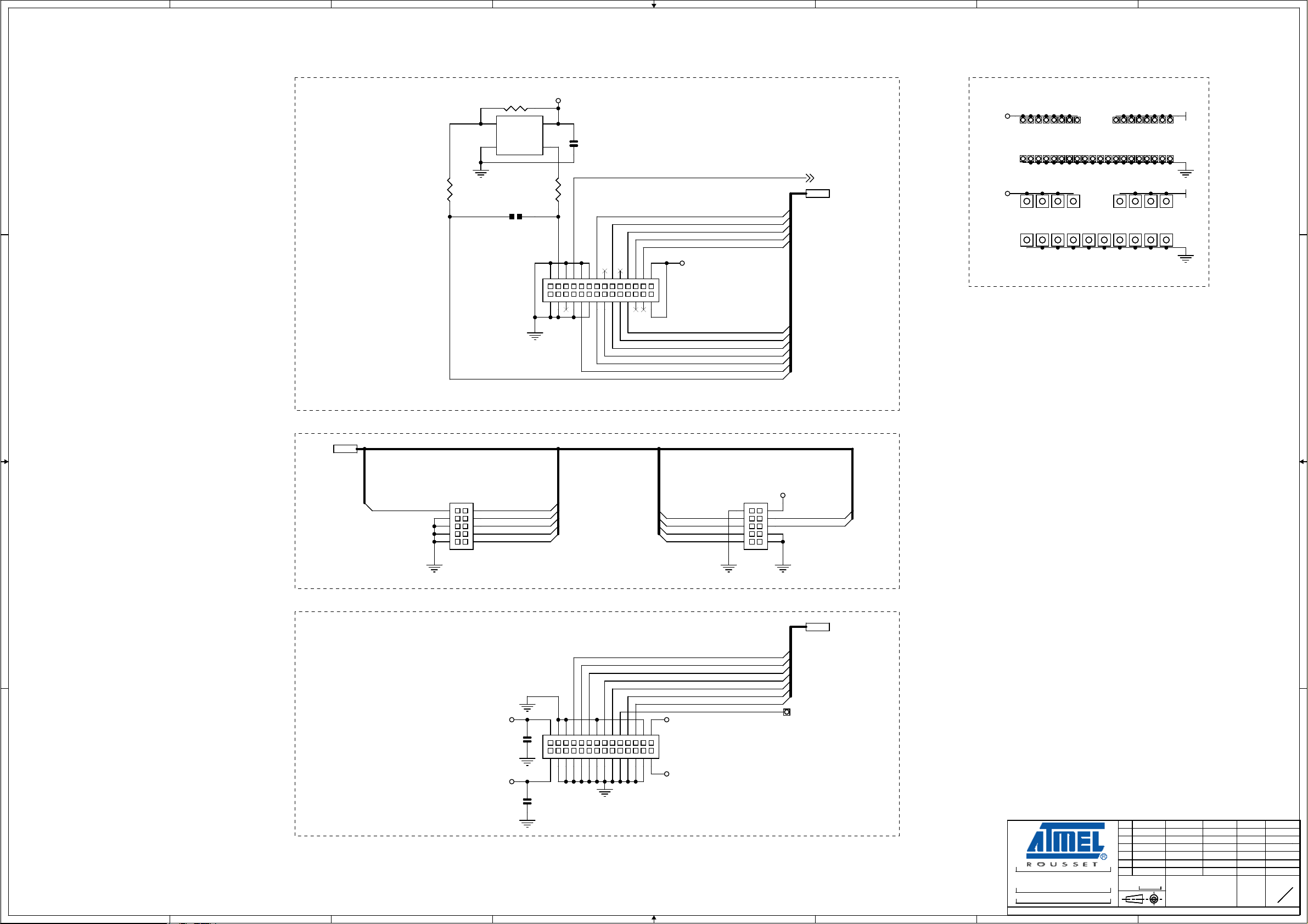
5.1 Schematics This section contains the following schematics:
! Processor Board
! I/O
! Ethernet
! RF modules
Section 5
Schematics
AT91SAM7X-EK Evaluation Board User Guide 5-1
6195E–ATARM–22-Mar-07

8
3V3
S1S1
Closed by 0R resistor
USB DEVICE INTERFACE
J6
USB BJ6USB B
1
4
D D
Q1
Q1
C19
C19
1µF
1µF
IN
1
2
C20
C20
1µF
1µF
5V
R4
470RR4470R
3
2
C C
B B
Si2302BDS
Si2302BDS
2
3
56
6
MN4
MN4
TPS73633
TPS73633
G
GND3OUT
4
C21
C21
10NF
10NF
DS5
DS5
YELLOW
YELLOW
1
POWER LED
5V
R20RR2
0R
EN5NR
3V3
TP1TP1
3V3
R6
100KR6100K
S6S6
7
3V3
3V3
6 1
3V3
3V3
5
MN1
MN1
USBUF02W6
USBUF02W6
PB25
6
5
4
3
2
1
JTAG INTERFACE
3V3
15234
S2S2
3V3_ADC
C6
C6
10µF
10µF
10V
10V
C13
C13
10NF
10NF
A1
A2
A3
A4
A5
A6
A7
A8
A9
A10
A11
A12
A13
A14
A15
A16
A17
A18
A19
A20
A21
A22
A23
A24
A25
A26
A27
A28
A29
A30
A31
A32
678
1 2
3 4
5 6
7 8
9 10
11 12
13
15
17
19
MN2
MN2
5
VOUT
4
VIN
LM4120AIM5-3.0
LM4120AIM5-3.0
VREF
J16AJ16A
J7J7
14
16
18
20
3V3_ADC
1
REF
2
GND
3
EN
GND_ADC
R3 1KR3 1K
PB0
B1
PB1
B2
PB2
B3
PB3
B4
PB4
B5
PB5
B6
PB6
B7
PB7
B8
PB8
B9
PB9
B10
PB10
B11
PB11
B12
PB12
B13
PB13
B14
PB14
B15
PB15
B16
PB16
B17
PB17
B18
PB18 RK
B19
PB19
B20
PB20
B21
PB21
B22
PB22
B23
PB23TIOA0
B24
PB24TIOB0
B25
PB25
B26
PB26
B27
PB27PWM0
B28
PB28PWM1
B29
PB29PCK1
B30
PB30
B31
B32
NRST
J16BJ16B
L1 4.7µHL1 4.7µH
C5
100NFC5100NF
R1 0RR1 0R
GND_ADC
RSSI
5V
RXD0
TXD0
SCK0
RTS0
CTS0
SPI0_MISO
SPI0_MOSI
SPI0_SPCK
SPI0_NPCS0
SPI0_NPCS1
TWD
TWCK
TF
TK
TD
RD
RF
TIOA0
TIOB0
PCK1
IRQ0
PWM0
PWM1
AD6
AD7
3V3
TP2TP2
PB[0..30]
3V3
S3S3
C1
C2
C3
C4
C5
C6
C7
C8
C9
C10
C11
C12
C13
C14
C15
C16
C17
C18
C19
C20
C21
C22
C23
C24
C25
C26
C27
C28
C29
C30
C31
C32
J16CJ16C
USART
SPI
TWI
SCC
TIMER
PCK
IRQ
PWM
RESERVED
ADC
MANUAL RESET
BP2BP2
2
34
3V3
J11J11
C8 10V10µFC8 10V10µF
C9 100NFC9 100NF
C10 100NFC10 100NF
C11 100NFC11 100NF
C12 100NFC12 100NF
C22
C22
C23 10pFC23 10pF
J17
J17
1
2 3
54
SMB
NOT POPULATED
NOT POPULATED
3V3
C14 100NFC14 100NF
C15 100NFC15 100NF
C16 100NFC16 100NF
C17 100NFC17 100NF
C18 100NFC18 100NF
10pF
10pF
Y1
Y1
18.432MHz
18.432MHz
VDDOUT1V8
C25 1NFC25 1NF
C26 10NFC26 10NF
VDDOUT1V8
J14J14
J15J15
S4S4
S5S5
J18J18
C24
C24
100NF
100NF
R5 1.5KR5 1.5K
C1
100
15
37
62
87
17
33
48
61
84
16
32
52
68
83
96
98
97
99
7
2
10V10µFC110V10µF
VDDOUT
VDDCORE
VDDCORE
VDDCORE
VDDCORE
VDDIO
VDDIO
VDDIO
VDDIO
VDDIO
GND
GND
GND
GND
GND
GND
GND
XOUT
XIN
VDDPLL
PLLRC
8
VDDIN
PA0/RXD081PA1/TXD082PA2/SCK0/SPI1_NPCS186PA3/RTS0/SPI1_NPCS285PA4/CTS0/SPI1_NPCS388PA5/RXD189PA6/TXD190PA7/SCK1/SPI0_NPCS191PA8/RTS1/SPI0_NPCS213PA11/TWCK19PA12/SPI0_NPCS0
C2
100NFC2100NF
93
94
DDP
DDM
AT91SAM7X256
AT91SAM7X256
AT91SAM7XC256
AT91SAM7XC256
PA10/TWD
PA9/CTS1/SPI0_NPCS3
18
14
3V3
J8J8
3V3
J12J12
95
92
ERASE
VDDFLASH
PA14/SPI0_NPCS2/IRQ122PA15/SPI0_NPCS3/TCLK223PA16/SPI0_MISO24PA17/SPI0_MOSI
PA18/SPI0_SPCK26PA19/CANRX46PA21/TF/SPI1_NPCS0
25
PA13/SPI0_NPCS1/PCK1
20
21
3V3
J10J10
J9J9
DNP
57
77
58
76
79
TST
NRST
PA20/CANTX47PA22/TK/SPI1_SPCK50PA23/TD/SPI1_MOSI55PA24/RD/SPI1_MISO56PA25/RK/SPI1_NPCS159PA26/RF/SPI1_NPCS260PA27/DRXD/PCK373PA28/DTXD
49
TCK
TDO
JTAGSEL
AD3/PWM3/PCK2/PB30
AD2/PWM2/PCK1/PB29
AD1/PWM1/TIOB2/PB28
AD0/PWM0/TIOA2/PB27
TCLK1/PWM0/PB19
ADTRG/EF100/PB18
SPI0_NPCS3/ERXCK/PB17
SPI1_NPCS3/ECOL/PB16
ERXDV/ECRSDV/PB15
SPI0_NPCS2/ERX3/PB14
SPI0_NPCS1/ERX2/PB13
TCLK0/ETXER/PB12
SPI1_NPCS2/ETX3/PB11
SPI1_NPCS1/ETX2/PB10
PCK0/EREFCK_ETXCK/PB0
78
51
TDI
TMS
ADVREF
AD7
AD6
AD5
AD4
RI1/TIOB1/PB26
DTR1/TIOA1/PB25
DSR1/TIOB0/PB24
DCD1/TIOA0/PB23
PCK2/PWM3/PB22
PCK1/PWM2/PB21
PCK0/PWM1/PB20
EMDIO/PB9
EMDC/PB8
ERXER/PB7
ERX1/PB6
ERX0/PB5
ECRS/PB4
ETX1/PB3
ETX0/PB2
ETXEN/PB1
PA29/FIQ/SPI1_NPCS375PA30/IRQ0/PCK2
74
80
C3
100NFC3100NF
1
6
5
4
3
12
11
10
9
72
71
70
69
67
66
65
64
63
36
53
35
29
30
39
45
44
27
28
38
31
34
54
43
42
41
40
3V3_ADC
PB30
PB29
PB28
PB27
PB26
PB25
PB24
PB23
PB22
PB21
PB20
PB19
PB18
PB17
PB16
PB15
PB14
PB13
PB12
PB11
PB10
PB9
PB8
PB7
PB6
PB5
PB4
PB3
PB2
PB1
PB0
C7
22NFC722NF
J13J13
AD7
AD6
AD5
AD4
123
C4
22NFC422NF
GND_ADC
RR1
RR1
100K
100K
3.00V +- 0.2%
PA0RXD0
PA1TXD0
PA2SCK0
PA3RTS0
PA4CTS0
PA5
PA6
PA7
PA8
PA9
PA10TWD
PA11TWCK
PA12SPI0_NPCS0
PA13SPI0_NPCS1
PA14
PA15
PA16SPI0_MISO
PA17SPI0_MOSI
PA18SPI0_SPCK
PA19
PA20
PA21TF
PA22TK
PA23TD
PA24RD
PA25RK
PA26RF
PA27
PA28
PA29
PA30IRQ0
PA16
PA3
PA1
PA0
PA2
PA4
PA9
PA5
PA8
PA6
PA7
PA14
PA13
PA15
PA10
PA11
PA12
PA19
PA17
PA18
PA20
DATAFLASH CARD SOCKET
J30
J30
FPS009
FPS009
8
7
6
5
4
3
2
1
9
6
C63
C63
100NF
100NF
SPI0_MISO
SPI0_SPCK
3V3
SPI0_MOSI
SPI0_NPCS1
PA16
PA18
PA17
PA13
PA16
PA17
PA18
PA12
3V3
SPI0_MISO
SPI0_MOSI
SPI0_SPCK
SPI0_NPCS0
J19J19
R7 100KR7 100K
NRST
5
A A
ADHESIVE FEET
Z7
11.1Z811.1
11.1Z711.1
8
Z10
Z9
11.1Z911.1
Z10
11.1
11.1
7
Z8
DATAFLASH MEMORY
MN5MN5
8
SO
1
SI
2
SCK
4
CS
3
RESET
WRITE PROTECT
VCC
GND
WP
6
7
5
PA25
PA23
PA22
PA21
PA24
3V3
C27
C27
100NF
100NF
S7S7
4
PA30
PA29
PA26
PA27
PA28
SERIAL EEPROM
MN11MN11
1
A0
2
A1
3
NC
7
WP
NOT POPULATED
3V3
SCL
SDA
VCC
GND
PA[0..30]
R39
C62
C62
100NF
100NF
3V3
R39
10K
10K
S28S28
S29S29
3
PA11
PA10
JPG 14/12/05C
JPG 14/12/05C
JPG 14/12/05C
30/09/05B JPG
30/09/05B JPG
INIT EDIT
INIT EDIT
INIT EDIT
A
A
A
REV
REV
AT91SAM7X-EK
AT91SAM7X-EK
AT91SAM7X-EK
AT91SAM7XC-EK
AT91SAM7XC-EK
AT91SAM7XC-EK
PROCESSOR BOARD
PROCESSOR BOARD
PROCESSOR BOARD
This agreement is our property. Reproduction and publication without our written authorization shall expose offender to legal proceedings.
This agreement is our property. Reproduction and publication without our written authorization shall expose offender to legal proceedings.
This agreement is our property. Reproduction and publication without our written authorization shall expose offender to legal proceedings.
2
REV
SCALE
SCALE
SCALE
1/1
1/1
1/1
JPG
JPG
JPG
DES.
DES.
DES.
30/09/05B JPG
13/09/05
13/09/05
13/09/05
DATE
DATE
DATE
1
VER.
VER.
VER.
DATEMODIF.
DATEMODIF.
DATEMODIF.
REV. SHEET
REV. SHEET
REV. SHEET
1
1
1
C
C
C
4
4
4
R38
R38
10K
10K
6
5
8
4

8
CAN
D D
C C
J20J20
1
2
3
RS232 COM PORT
1
6
RXD
2
RTS
7
TXD
3
CTS
8
4
9
5
10
11
J24
J24
MALE RIGHT ANGLED
MALE RIGHT ANGLED
R8
120R8120
J21J21
C34
C34
100NF
100NF
C37
C37
100NF
100NF
3V3
C32
C32
100NF
100NF
7
MN6
MN6
7
CANH
6
CANL
TJA1050T
TJA1050T
VCC
VCC
15
GND
GND
2
V+
V+
6
14
7
13
ADM3202ARN
ADM3202ARN
R
R
R
R
TXD
RXD
RS
VREF
VCC
GND
MN8
MN8
C1+
C1+
C1-
C1C2+
C2+
C2-V-
C2-V-
T
T
T
T
C28
C28
100NF
100NF
6
3V3
PA[0..30]
R41
3V3
TXD0
RTS0
RXD0
CTS0
R41
10K
10K
S11S11
S8S8
S9S9
S10S10
S13S13
S14S14
S15S15
S16S16
PA20
PA19
PA2
PA1
PA3
PA0
PA4
R40
R40
100K
100K
1
4
8
C29
C29
5
10µF
10µF
R42 0RR42 0R
10V
10V
3
2
116
100NF
100NF
3
4
100NF
100NF
5
11
10
12
98
R43
R43
NOT POPULATED
NOT POPULATED
C33
C33
C35
C35
R13
R13
100K
100K
3V3
R14
R14
100K
100K
5V
5
C30
C30
3 2
3
2
GND_ADC
3V3_ADC
MN7B
MN7B
AD8030AR
AD8030AR
7
GND_ADC
3V3
PB30
S12S12
R12
R12
PB19
100K
100K
AD5
AD4
VREF
1
PWM3
1
S17S17
1µF
1µF
GND_ADC
Q2
Q2
Si2301BDS
Si2301BDS
R9 1KR9 1K
R11 1KR11 1K
Q3
Q3
Si2302BDS
Si2302BDS
8
+
+
-
-
4
R16 180RR16 180R
4
R10 6,20K 1%R10 6,20K 1%
GND_ADC
C36 100NFC36 100NF
C38 10µFC38 10µF
5
6
GND_ADC
GREEN
GREEN
R151KR15
C39
C39
100NF
100NF
C31
C31
1µF
1µF
GND_ADC
1K
DS1
DS1
MN7A
MN7A
AD8030AR
AD8030AR
3
+
+
2
-
-
3V3
1
3
1
2
3
GND_ADC
J26J26
PB[0..30]
I/O ANALOG
CONNECTOR
2
1
B B
DS2
GREEN
3V3
C40
C40
100NF
SERIAL DEBUG PORT
100NF
C42
C42
100NF
1
6
RXD
2
7
TXD
3
8
4
9
5
10
11
J25
J25
A A
MALE RIGHT ANGLED
MALE RIGHT ANGLED
8
100NF
C44
C44
100NF
100NF
15
2
6
14
7
13
ADM3202ARN
ADM3202ARN
7
V+
V+
VCC
VCC
GND
GND
MN9
MN9
C1+
C1+
C1-
C1C2+
C2+
C2-V-
C2-V-
T
T
T
T
R
R
R
R
C41
C41
116
100NF
100NF
3
4
100NF
100NF
5
11
10
12
98
C43
C43
3V3
R18
R18
100K
100K
6
DBGU_TXD
DBGU_RXD
S21S21
S22S22
PA28
PA27
5
PB20
PB21
PB22
USER INTERFACE
S18S18
S19S19
S20S20
R17 180RR17 180R
R19 180RR19 180R
R20 180RR20 180R
GREEN
GREEN
GREEN
GREEN
GREEN
4
DS2
DS3
DS3
DS4
DS4
PA24
PA21
PA23
PA25
PA22
LEFT
3
BP1BP1
1
3 6
JOYSTICK
4
52
UP
RIGHT
DOWNPUSH
14/12/05JPGC
14/12/05JPGC
14/12/05JPGC
30/09/05B JPG
30/09/05B JPG
INIT EDIT
INIT EDIT
INIT EDIT
A
A
A
REV
REV
AT91SAM7X-EK
AT91SAM7X-EK
AT91SAM7X-EK
AT91SAM7XC-EK
AT91SAM7XC-EK
AT91SAM7XC-EK
I/O
I/O
I/O
This agreement is our property. Reproduction and publication without our written authorization shall expose offender to legal proceedings.
This agreement is our property. Reproduction and publication without our written authorization shall expose offender to legal proceedings.
This agreement is our property. Reproduction and publication without our written authorization shall expose offender to legal proceedings.
2
REV
SCALE
SCALE
SCALE
1/1
1/1
1/1
JPG
JPG
JPG
DES.
DES.
DES.
30/09/05B JPG
13/09/05
13/09/05
13/09/05
DATE
DATE
DATE
1
VER.
VER.
VER.
DATEMODIF.
DATEMODIF.
DATEMODIF.
REV. SHEET
REV. SHEET
REV. SHEET
2
2
2
C
C
C
4
4
4

8
7
6
5
4
3
2
1
3V3
Y2
D D
C C
B B
R21
R21
PB[0..30]
10K
10K
Y2
OE
OE
50 MHz
50 MHz
VSS OUT
VSS OUT
SG-8002JC-50.0000M-PCB
SG-8002JC-50.0000M-PCB
VDD
VDD
NRST
41
32
PB0
PB11
PB10
PB3
PB2
PB1
PB14
PB13
PB6
PB5
PB17
PB15
PB12
PB7
PB16
PB4
PB8
PB9
PB26
PB18
REFCK
ETX3
ETX2
ETX1
ETX0
ETXEN
ERX3
ERX2
ERX1
ERX0
ERXCK
ERXDV
ETXER
ERXER
ECOL
ECRS
EMDC
EMDIO
IRQ
3V3
C45
C45
100NF
100NF
3V3
S23S23
R27 10KR27 10K
Cut
Closed by 0R resistor
R26 10KR26 10K C53
J28J28
Closed by 0R resistor
S25S25
100NF
100NF
C54
C54
100NF
100NF
C55
C55
100NF
100NF
C56
C56
Cut
S26S26
MII Factory setting
C46
C46
22PF
22PF
25MHz
25MHz
1 2
DM9161AE
DM9161AE
CABLESTS/LINKSTS
3V3
42
17
18
19
20
21
22
26
27
28
29
34
37
16
38
36
35
24
25
32
39
41
30
23
15
33
44
10
40
S24S24
MN10
MN10
REF_CLK/XT2
TXD3
TXD2
TXD1
TXD0
TX_EN
TX_CLK/ISOLATE
RXD3/PHYAD3
RXD2/PHYAD2
RXD1/PHYAD1
RXD0/PHYAD0
RX_CLK/10BTSER
RX_DV/TESTMODE
TX_ER/TXD4
RX_ER/RXD4/RPTR
COL/RMII
CRS/PHYAD4
MDC
MDIO
MDINTR
DISMDIX
DVDD
DVDD
DVDD
DGND
DGND
DGND
PWRDWN
RESET
C47
C47
22PF
22PF
Y3
Y3
C48 100NFC48 100NF
R23
XT1
TX+
TX-
RX+
RX-
AVDDR
AVDDR
AVDDT
AGND
AGND
AGND
BGRESG
BGRES
LEDMODE
LED0/OP0
LED1/OP1
LED2/OP2
N.C
43
7
8
3
4
1
2
9
5
6
46
47
48
31
11
12
13
14
45
VCCA
R28
R28
6,80K 1%
6,80K 1%
R30 10KR30 10K
C49
C49
100NF
100NF
C51
C51
100NF
100NF
C52
C52
100NF
100NF
3V3
L2 742792093L2 742792093
C50
C50
10V
10V
10µF
10µF
DS6
DS6
DS7
DS7
DS8
DS8
VCCA
YELLOW
YELLOW
GREEN
GREEN
GREEN
GREEN
R22
R22
49R9
49R9
1%
1%
R24
R24
49R9
49R9
1%
1%
FULL DUPLEX
SPEED 100
LINK&ACT
R23
49R9
49R9
1%
1%
R25
R25
49R9
49R9
1%
1%
C53
100NF
100NF
R291KR29
R31 1KR31 1K
R32 1KR32 1K
15
J27
J27
TD+
TD+
1
CT
CT
4
TD-
TD-
2
RD+
RD+
3
CT
CT
5
RD-
RD-
6
NC
NC
7
8
J00-0061
J00-0061
1nF
1nF
16
7575
7575
75
75
75
75
TX+
TX+
TX-
TX-
RX+
RX+
RX-
RX-
1
1
2
2
3
3
6
6
4
4
5
5
7
7
8
8
RJ45 ETHERNET CONNECTOR
1K
3V3
NOT POPULATED
3V3 VCCA
L3 4.7µHL3 4.7µH
C58
C57
C57
10µF
10µF
10V
10V
R33 0RR33 0R
A A
8
7
6
5
C58
100NF
100NF
R34 0RR34 0R
C59
C59
10µF
10µF
10V
10V
C60
C60
100NF
100NF
JPG 14/12/05C
JPG 14/12/05C
JPG 14/12/05C
30/09/05B JPG
30/09/05B JPG
INIT EDIT
INIT EDIT
INIT EDIT
A
A
A
REV
REV
AT91SAM7X-EK
AT91SAM7X-EK
AT91SAM7X-EK
AT91SAM7XC-EK
AT91SAM7XC-EK
AT91SAM7XC-EK
ETHERNET
ETHERNET
ETHERNET
This agreement is our property. Reproduction and publication without our written authorization shall expose offender to legal proceedings.
This agreement is our property. Reproduction and publication without our written authorization shall expose offender to legal proceedings.
4
3
This agreement is our property. Reproduction and publication without our written authorization shall expose offender to legal proceedings.
2
REV
SCALE
SCALE
SCALE
1/1
1/1
1/1
JPG
JPG
JPG
DES.
DES.
DES.
30/09/05B JPG
13/09/05
13/09/05
13/09/05
DATE
DATE
DATE
1
VER.
VER.
VER.
DATEMODIF.
DATEMODIF.
DATEMODIF.
REV. SHEET
REV. SHEET
REV. SHEET
3
3
3
C
C
C
4
4
4
8
7
6
5
4
3
2
1
ATR2406 2.4 GHz RF CONNECTORS MODULE
Y4 SG-8002JC-13.8240M-PCB
Y4 SG-8002JC-13.8240M-PCB
R35
R35
10K
10K
OE
D D
R360RR36
0R
C C
OE
VSS OUT
VSS OUT
VDD
VDD
13.824 MHz
13.824 MHz
S27S27
R370RR37
0R
J29J29
3V3
41
C61
32
C61
100NF
100NF
RSSI
PA[0..30]
GPIO
SPI0_SPCK
GPIO
TXD1
GPIO
REF_CLK
2122
2324
2526
2728
111213151719
141618
20
12345678910
3V3
SPI0_NPCS3
SPI0_MOSI
GPIO
GPIO
SCK1
RXD1
GPIO/PCK2 OSC REMOTE OR REF_CLK
PA26
PA18
PA8
PA6
PA14
PA15
PA17
PA29
PA9
PA7
PA5
PA30
RX_ON
CLOCK
PU_TRX
TX_DATA
TX_ON
ENABLE
DATA
nOLE
PU_REG
RX-CLOCK
RX_DATA
USER'S GRID AERA
5V3V3
1.27 PITCH
5V3V3
2.54 PITCH
NOT POPULATED
AT86RF210 ZIGBEE CONNECTORS MODULE
PA[0..30]
3V3
PA26 PA14
B B
NOT POPULATED
J4J4
GPIOGPIO
12
34
SPI0_SPCK
56
SPI0_MOSI
78
SPI0_MISO
910
PA15
PA18
PA17
PA16
TXRX
SEL
SCLK
SDI
SDO TX_DATA
CHIP_READY
RX_DATA_CLK
RX_DATA
PA9
PA7
PA5
PA6
SCK1
RXD1
TXD1
J5J5
9 10
7 8
5 6
3 4
1 2
GPIOGPIO
GPIO
PA29
PA8
CCASPI0_NPCS3
START
AT86RF230 CONNECTORS MODULE
PA[0..30]
PA29
PA15
PA17
PA16
PA18
PA8
PA9
IRQ
SEL
MOSI
MISO
SCLK
SLP_TR
RSTN
16 MHz CLOCK
3V3 3V3
C64
C64
100NF
100NF
141618
20
J31J31
FIQ
SPI0_NPCS3
SPI0_MOSI
SPI0_MISO
SPI0_SPCK
GPIO
GPIO
21 22
23 24
25 26
27 28
3V3
C65
C65
100NF
A A
100NF
11 1213151719
3V3
1 2
3 4
5 6
7 8
9 10
NOT POPULATED
14/12/05JPGC
14/12/05JPGC
14/12/05JPGC
30/09/05B JPG
30/09/05B JPG
INIT EDIT
INIT EDIT
INIT EDIT
A
A
A
REV
REV
AT91SAM7X-EK
AT91SAM7X-EK
AT91SAM7X-EK
AT91SAM7XC-EK
AT91SAM7XC-EK
AT91SAM7XC-EK
RF MODULES
RF MODULES
RF MODULES
This agreement is our property. Reproduction and publication without our written authorization shall expose offender to legal proceedings.
This agreement is our property. Reproduction and publication without our written authorization shall expose offender to legal proceedings.
8
7
6
5
4
3
This agreement is our property. Reproduction and publication without our written authorization shall expose offender to legal proceedings.
2
REV
SCALE
SCALE
SCALE
1/1
1/1
1/1
JPG
JPG
JPG
DES.
DES.
DES.
30/09/05B JPG
13/09/05
13/09/05
13/09/05
DATE
DATE
DATE
1
VER.
VER.
VER.
DATEMODIF.
DATEMODIF.
DATEMODIF.
REV. SHEET
REV. SHEET
REV. SHEET
4
4
4
C
C
C
4
4
4

Schematics
5-2 AT91SAM7X-EK Evaluation Board User Guide
6195E–ATARM–22-Mar-07

Section 6
Errata
6.1 DM9161A Ethernet Phy Connections
6.2 TWI line pullups for Fast Mode operation
The Ethernet interface works as presented in the schematics, but the connections are
not in compliance with Davicom recommendations.
To comply with Davicom recommendations on connecting this device, J27-4 and J27-5
(RJ45 connector, CT) should be connected to the VCCA side of L2. In the current schematics (ETHERNET, Sheet 3/4), the VCCA side of L2 is connected to MN10-1 and
MN10-2 (DM9161A, AVDDR).
For additional information, refer to the Davicom datasheet for DM9161A and associated
Application Notes available on http://www.davicom.com.tw/.
In order to use the TWI in Fast Mode (up to 400 Kbits/s), the default 10 KΩ resistors R38
and R39 should be replaced by smaller values (e.g., 2.2 KΩ).
Note that there is no need to change the pull-up resistors if the TWI is used in Standard
Mode (up to 100 Kbits/s).
AT91SAM7X-EK Evaluation Board User Guide 6-1
6195E–ATARM–22-Mar-07

Errata
6-2 AT91SAM7X-EK Evaluation Board User Guide
6195E–ATARM–22-Mar-07

Revision History
7.1 Revision History
Table 7-1. Change History
Document Comments
6195A First issue.
6195B Updated
functionalities. New board block diagram and schematics issued.
6195C Updated document to contain new product AT91SAM7XC.
Added new section with Errata.
6195D Removed references to 32 Mbit serial DataFlash (AT45DB321C-CNC) in
and in Section 3.6. Inserted new Figure 2-3 and new schematics in Section 5.
Figure 2-3 with new signal names. Updated document to show new product
Section 1.3
Section 7
Change Request
Ref.
05-430
2862
6195E Added Errata
Section 6.2 ”TWI line pullups for Fast Mode operation” 4084
AT91SAM7X-EK Evaluation Board User Guide 7-1
6195E–ATARM–22-Mar-07

Revision History
7-2 AT91SAM7X-EK Evaluation Board User Guide
6195E–ATARM–22-Mar-07

Atmel Corporation Atmel Operations
2325 Orchard Parkway
San Jose, CA 95131, USA
Tel: 1(408) 441-0311
Fax: 1(408) 487-2600
Regional Headquarters
Atmel Europe
Le Krebs
8, rue Jean-Pierre Timbaud
BP 309
78054 Saint-Quentin-en-Yvelines
Cedex
France
Tel: (33) 1-30-60-70-00
Fax: (33) 1-30-60-71-11
Asia
Room 1219
Chinachem Golden Plaza
77 Mody Road Tsimshatsui
East Kowloon
Hong Kong
Tel: (852) 2721-9778
Fax: (852) 2722-1369
Japan
9F, Tonetsu Shinkawa Bldg.
1-24-8 Shinkawa
Chuo-ku, Tokyo 104-0033
Japan
Tel: (81) 3-3523-3551
Fax: (81) 3-3523-7581
Memory
2325 Orchard Parkway
San Jose, CA 95131, USA
Tel: 1(408) 441-0311
Fax: 1(408) 436-4314
Microcontrollers
2325 Orchard Parkway
San Jose, CA 95131, USA
Tel: 1(408) 441-0311
Fax: 1(408) 436-4314
La Chantrerie
BP 70602
44306 Nantes Cedex 3, France
Tel: (33) 2-40-18-18-18
Fax: (33) 2-40-18-19-60
ASIC/ASSP/Smart Cards
Zone Industrielle
13106 Rousset Cedex, France
Tel: (33) 4-42-53-60-00
Fax: (33) 4-42-53-60-01
1150 East Cheyenne Mtn. Blvd.
Colorado Springs, CO 80906, USA
Tel: 1(719) 576-3300
Fax: 1(719) 540-1759
Scottish Enterprise Technology Park
Maxwell Building
East Kilbride G75 0QR, Scotland
Tel: (44) 1355-803-000
Fax: (44) 1355-242-743
RF/Automotive
Theresienstrasse 2
Postfach 3535
74025 Heilbronn, Germany
Tel: (49) 71-31-67-0
Fax: (49) 71-31-67-2340
1150 East Cheyenne Mtn. Blvd.
Colorado Springs, CO 80906, USA
Tel: 1(719) 576-3300
Fax: 1(719) 540-1759
Biometrics
Avenue de Rochepleine
BP 123
38521 Saint-Egreve Cedex, France
Tel: (33) 4-76-58-47-50
Fax: (33) 4-76-58-47-60
Literature Requests
www.atmel.com/literature
Disclaimer: The information in this document is provided in connection with Atmel products. No license, express or implied, by estoppel or otherwise, to any
intellectual property right is granted by this document or in connection with the sale of Atmel products. EXCEPT AS SET FORTH IN ATMEL’S TERMS AND CONDI-
TIONS OF SALE LOCATED ON ATMEL’S WEB SITE, ATMEL ASSUMES NO LIABILITY WHATSOEVER AND DISCLAIMS ANY EXPRESS, IMPLIED OR STATUTORY
WARRANTY RELATING TO ITS PRODUCTS INCLUDING, BUT NOT LIMITED TO, THE IMPLIED WARRANTY OF MERCHANTABILITY, FITNESS FOR A PARTICULAR
PURPOSE, OR NON-INFRINGEMENT. IN NO EVENT SHALL ATMEL BE LIABLE FOR ANY DIRECT, INDIRECT, CONSEQUENTIAL, PUNITIVE, SPECIAL OR INCIDENTAL DAMAGES (INCLUDING, WITHOUT LIMITATION, DAMAGES FOR LOSS OF PROFITS, BUSINESS INTERRUPTION, OR LOSS OF INFORMATION) ARISING OUT
OF THE USE OR INABILITY TO USE THIS DOCUMENT, EVEN IF ATMEL HAS BEEN ADVISED OF THE POSSIBILITY OF SUCH DAMAGES. Atmel makes no
representations or warranties with respect to the accuracy or completeness of the contents of this document and reserves the right to make changes to specifications
and product descriptions at any time without notice. Atmel does not make any commitment to update the information contained herein. Unless specifically provided
otherwise, Atmel products are not suitable for, and shall not be used in, automotive applications. Atmel’s products are not intended, authorized, or warranted for use
as components in applications intended to support or sustain life.
© 2007 Atmel Corporation. All rights reserved. Atmel®, logo and combinations thereof, and Everywhere You Are®, DataFlash® and others are
registered trademarks, SAM-BA
ARM7TDMI
of others.
®
, Thumb® and others are the registered trademarks or trademarks of ARM Ltd. Other terms and product names may be trademarks
™
and others are trademarks of Atmel Corporation or its subsidiaries. ARM®, the ARM Powered® logo,
Printed on recycled paper.
6195E–ATARM–22-Mar-07
 Loading...