

Page 1

AT91SAM7SE-EK Evaluation Board
..............................................................................................
User Guide
Page 2

-2 AT91SAM7SE-EK Evaluation Board User Guide
6241B–ATARM–22-Mar-07
Page 3

Table of Contents
Section 1
Overview...............................................................................................1-1
1.1 Scope........................................................................................................1-1
1.2 Deliverables ..............................................................................................1-1
1.3 AT91SAM7SE-EK Evaluation Board ........................................................1-1
Section 2
Setting Up the AT91SAM7SE-EK Board ..............................................2-1
2.1 Electrostatic Warning ................................................................................2-1
2.2 Requirements............................................................................................2-1
2.3 Layout .......................................................................................................2-2
2.4 Powering Up the Board.............................................................................2-3
2.5 Getting Started..........................................................................................2-3
2.6 AT91SAM7SE-EK Block Diagram ............................................................2-4
Section 3
Board Description .................................................................................3-1
3.1 AT91SAM7SE Microcontroller ..................................................................3-1
3.2 AT91SAM7SE Block Diagram ..................................................................3-4
3.3 Memory .....................................................................................................3-5
3.4 Clock Circuitry...........................................................................................3-5
3.5 Reset Circuitry ..........................................................................................3-5
3.6 Power Supply Circuitry..............................................................................3-5
3.7 Remote Communication ...........................................................................3-5
3.8 Audio Stereo Interface ..............................................................................3-5
3.9 User Interface ...........................................................................................3-5
3.10 Debug Interface ........................................................................................3-5
3.11 Expansion Slot ..........................................................................................3-5
3.12 PIO Usage ................................................................................................3-6
Section 4
Configuration ........................................................................................4-1
4.1 Jumpers ....................................................................................................4-1
4.2 Audio Configuration ..................................................................................4-1
4.3 JTAG/ICE..................................................................................................4-2
4.4 Microcontroller Clock ................................................................................4-2
4.5 Memory .....................................................................................................4-2
4.6 Ethernet ....................................................................................................4-2
4.7 Miscellaneous ...........................................................................................4-3
AT91SAM7SE-EK Evaluation Board User Guide -i
6241B–ATARM–22-Mar-07
Page 4

Section 5
Schematics ...........................................................................................5-1
5.1 Schematics ...............................................................................................5-1
Section 6
Errata....................................................................................................6-1
6.1 PIO Usage ................................................................................................6-1
6.2 TWI line pullups are too weak for Fast Mode operation............................6-1
Section 7
Revision History....................................................................................7-1
7.1 Revision History ........................................................................................7-1
-ii AT91SAM7SE-EK Evaluation Board User Guide
6241B–ATARM–22-Mar-07
Page 5

Section 1
Overview
1.1 Scope The AT91SAM7SE-EK evaluation board enables the evaluation of and code develop-
ment for applications running on an AT91SAM7SE device.
This guide focuses on the AT91SAM7SE-EK board as an evaluation platform.
1.2 Deliverables
1.2.1 Standard Version AT91SAM7S-EK VAR
1.3 AT91SAM7SEEK Evaluation
Board
The AT91SAM7SE-EK package contains the following items:
! An AT91SAM7SE-EK board
! One Universal input AC/DC power supply with US and Europe plug adapter
! One A/B-type USB cable
! One serial RS232 cable
! One CD-ROM containing summary and full datasheets, datasheets with electrical and
mechanical characteristics, application notes and getting started documents for all
development boards and AT91 microcontrollers. An AT91 software package with C
and assembly listings is also provided. This allows the user to begin evaluating the
AT91 A R M
The board is equipped with an AT91SAM7SE512 (128-pin LQFP package) together with
the following:
! 32 Mbytes of SDRAM memory
! 256 Mbytes of NAND Flash memory
! One USB device port interface
! One DBGU serial communication port
®
Thumb® 32-bit microcontroller quickly.
! One additional serial communication port with RTS/CTS handshake control
! One JTAG/ICE debug interface
! One Atmel AT73C213 Stereo Audio DAC
AT91SAM7SE-EK Evaluation Board User Guide 1-1
6241B–ATARM–22-Mar-07
Page 6

Overview
! One power LED and two general-purpose LEDs
! One joystick and two user input pushbuttons
! One Reset pushbutton
! Three expansion connectors (PIO A, PIO B, PIO C)
! One EBI expansion BGA-like footprint connector
1-2 AT91SAM7SE-EK Evaluation Board User Guide
6241B–ATARM–22-Mar-07
Page 7

Section 2
Setting Up the AT91SAM7SE-EK
Board
2.1 Electrostatic Warning
2.2 Requirements In order to set up the AT91SAM7SE-EK evaluation board, the following items are
The AT91SAM7SE-EK evaluation board is shipped in protective anti-static packaging.
The board must not be subjected to high electrostatic potentials. A grounding strap or
similar protective device should be worn when handling the board. Avoid touching the
component pins or any other metallic element.
needed:
! The AT91SAM7SE-EK evaluation board itself.
! AC/DC power adapter (5V at 2A), 2.1 mm x 5.5 mm
AT91SAM7SE-EK Evaluation Board User Guide 2-1
6241B–ATARM–22-Mar-07
Page 8
Setting Up the AT91SAM7SE-EK Board
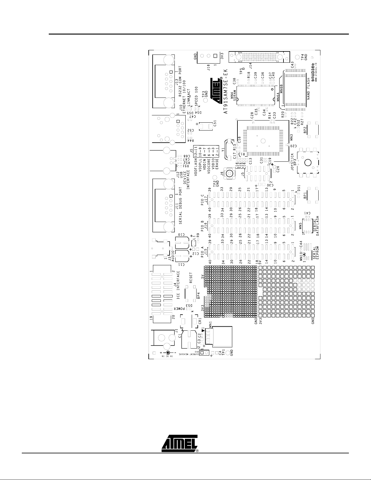
2.3 Layout Figure 2-1. AT91SAM7SE-EK Layout - Top View
2-2 AT91SAM7SE-EK Evaluation Board User Guide
6241B–ATARM–22-Mar-07
Page 9
Setting Up the AT91SAM7SE-EK Board
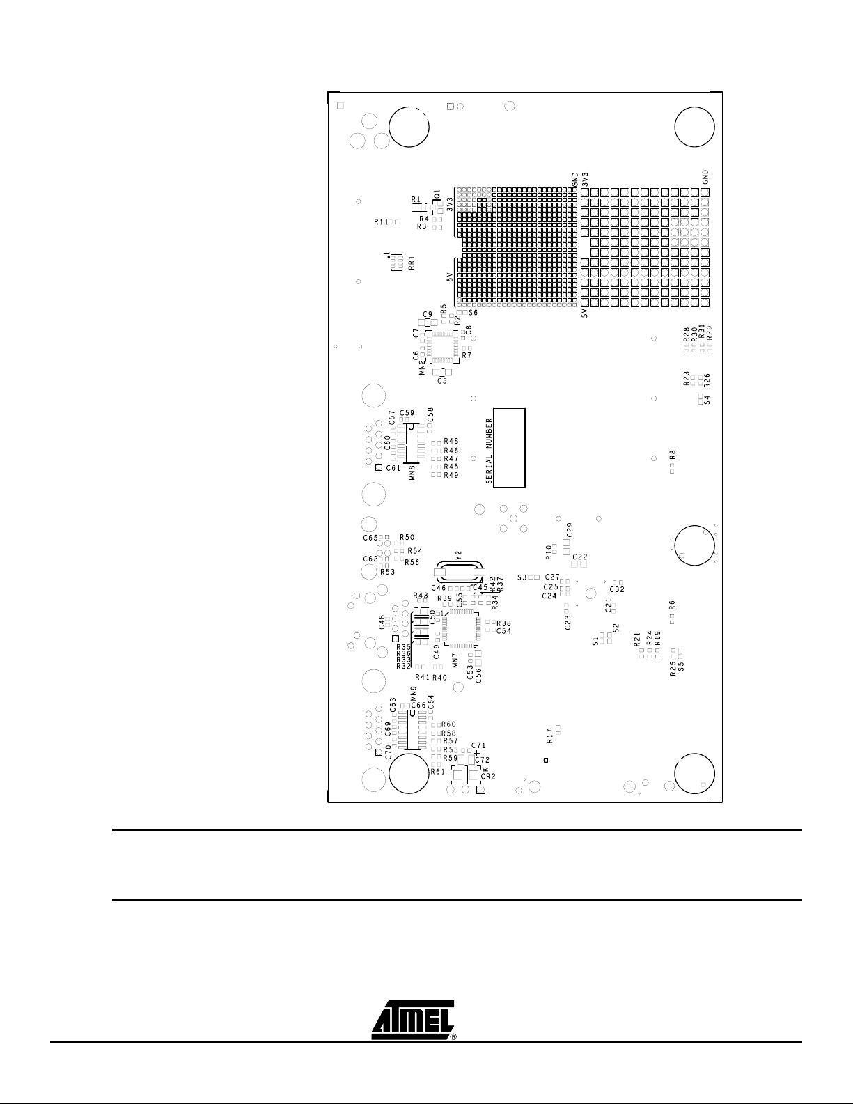
Figure 2-2. AT91SAM7SE-EK Layout - Bottom View
2.4 Powering Up the Board
The AT91SAM7SE-EK requires 5V DC (±5%). DC power is supplied to the board via the
2.1 mm x 5.5 mm socket J1. Coaxial plug center positive standard.
2.5 Getting Started The AT91SAM7SE-EK evaluation board is delivered with a CD-ROM containing all nec-
essary information and step-by-step procedures for working with the most common
development toolchains. Please refer to this CD-ROM, or to the AT91 web site,
http://www.atmel.com/products/AT91/, for the most up-to-date information on getting
started with the AT91SAM7SE-EK.
AT91SAM7SE-EK Evaluation Board User Guide 2-3
6241B–ATARM–22-Mar-07
Page 10
Setting Up the AT91SAM7SE-EK Board
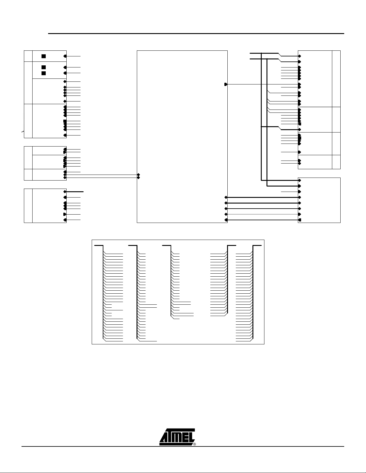
2.6 AT91SAM7SE-EK Block Diagram
POWER SUPPLY
5VDC
USER'S INTERFACE
DAC
01 - POWER SUPPLY
SERIAL INTERFACES
POWERLED
USERLED1
USERLED2
RIGHTCLIC
PUSHLEFTCLIC
AT73C213
DBGU
RS232FAST ETHERNET
COM0
DEVICE
USB
05 - COMMUNICATION
RMII_MII ETHERNET
NOT
POPULATED
03 - RMII_MII ETHERNET
PWM0
PWM1
PWM2
PB22
PB23
UP
PB24
DOWN
PB27
LEFT
PB26
RIGHT
PB25
PCK2
MCLK
TD
SDIN
TF
LRFS
TK
BCLK
MISO
DOUT
MOSI
DIN
SPCK
CLK
NPCS1
CS
NRST
NRST
DTXD
DTXD
DRXD NRST
DRXD
TXD0
TXD
RXD0
RXD
RTS0
RTS
CTS0
CTS
PC19
USBCNX
DDM
DDP
D[0..15]
CMD
IOW
PWRST
D[0..15]
A12
NWE
NRD
IOR
NCS2
CS
IRQ1
INT
NRST
DDM
DDP
02 - AT91SAM7SE
AT91SAM7SE
SDCK
PA[0..31]
PB[0..31]
PC[0..23]
NRST
AD[4..7]
PA[0..31]
PB[0..31]
PC[0..23]
NRST
AD[4..7]
D[0..31]
A[0..22]
MEMORY
D[0..15]
A[2..14]
RAS
CAS
SDA10
SDWE
SDCS
SDCK
SDCKE
A0
NBS1
A16
A17
A22
A21
NANDOE
NANDWE
NANDCS
RDYBSY
D[0..15]
MOSI
MISO
SPCK
NPCS0
TWCK
TWD
03 - MEMORY
EXPANSION CONNECTORS
SDCK
06 - EXPANSION CONNECTORS
D[0..15]
A[2..14]
RAS
CAS
SDA10
SDWE
SDCS
SDCK
SDCKE
NBS0
NBS1
BA0
BA1
CLE
ALE
NANDOE
NANDWE
NANDCS
RDYBSY
D[0..15]
SI
SO
SCK
CS
POPULATED
NRST
SCL
SDA
POPULATED
D[0..31]
A[0..22]
SDCK
PA[0..31]
PB[0..31]
PC[0..23]
NRST
AD[4..7]
NOT
NOT
SDRAMNANFLASH
DATAFLASH
SERIAL SERIAL
EEPROM
PIO USAGE
PA0 PWM0
PA1 PWM1
PA2 PWM2
PA3 TWD
PA4 TWCK
PA5 RXD0
PA6 TXD0
PA7 RTS0
PA8 CTS0
PA9 DRXD
PA10 DTXD
PA11 NPCS0
PA12 MISO
PA13 MOSI
PA14 SPCK
PA15 TF
PA16 TK
PA17 TD
PA18
PA19
PA20 NCS2
PA21
PA22
PA23 NBS1
PA24 SDA10
PA25 SDCKE
PA26 SDCS
PA27 SDWE
PA28 CAS
PA29 RAS
PA30 IRQ1
PA31 NPCS1
PB[0..31]
PB0
PB1
PB2
PB3
PB4
PB5
PB6
PB7
PB8
PB9
PB10
PB11
PB12
PB13
PB14
PB15
PB16
PB17
PB18 NANDCS
PB19 RDYBSY
PB20
PB21
PB22
PB23
PB24
PB25
PB26
PB27
PB28
PB29
PB30
PB31 PCK2
PC[0..23]
PC0
PC1
PC2
PC3
PC4
PC5
PC6
PC7
PC8
PC9
PC10
PC11
PC12
PC13
PC14
PC15
PC16
PC17 NANDOE
PC18 NANDWE
PC19
PC20
PC21 NWE
PC22 NRD
PC23
A[0..22]
A0PB0
A1PB1
A2PB2
A3PB3
A4PB4
A5PB5
A6PB6
A7PB7
A8PB8
A9PB9
A10PB10
A11PB11
A12PB12
A13PB13
A14PB14
A15PB15
A16PB16
A17PB17
A18PC16
A19PC17
A20PC18
A21PC19
A22PC20
D[0..31]PA[0..31]
D0PC0
D1PC1
D2PC2
D3PC3
D4PC4
D5PC5
D6PC6
D7PC7
D8PC8
D9PC9
D10PC10
D11PC11
D12PC12
D13PC13
D14PC14
D15PC15
D16PB18
D17PB19
D18PB20
D19PB21
D20PB22
D21PB23
D22PB24
D23PB25
D24PB26
D25PB27
D26PB28
D27PB29
D28PB30
D29PB31
D30PA30
D31PA31
2-4 AT91SAM7SE-EK Evaluation Board User Guide
6241B–ATARM–22-Mar-07
Page 11

Section 3
Board Description
3.1 AT91SAM7SE Microcontroller
• Incorporates the ARM7TDMI® ARM® Thumb® Processor
– High-performance 32-bit RISC Architecture
– High-density 16-bit Instruction Set
– Leader in MIPS/Watt
– EmbeddedICE
• Internal High-speed Flash
– 512 Kbytes, Organized in Two Contiguous Banks of 1024 Pages of 256 Bytes
Dual Plane (AT91SAM7SE512)
– 256 Kbytes (AT91SAM7SE256) Organized in One Bank of 1024 Pages of 256
Bytes Single Plane (AT91SAM7SE256)
– 32 Kbytes (AT91SAM7SE32) Organized in One Bank of 256 Pages of 128 Bytes
Single Plane (AT91SAM7SE32)
– Single Cycle Access at Up to 30 MHz in Worst Case Conditions
– Prefetch Buffer Optimizing Thumb Instruction Execution at Maximum Speed
– Page Programming Time: 6 ms, Including Page Auto-erase, Full Erase Time: 15
ms
– 10,000 Erase Cycles, 10-year Data Retention Capability, Sector Lock Capabilities,
Flash Security Bit
– Fast Flash Programming Interface for High Volume Production
• 32 Kbytes (AT91SAM7SE512/256) or 8 Kbytes (AT91SAM7SE32) of Internal
High-speed SRAM, Single-cycle Access at Maximum Speed
• One External Bus Interface (EBI)
– Supports SDRAM, Static Memory, Glueless Connection to CompactFlash
ECC-enabled NANDFlash
• Memory Controller (MC)
– Embedded Flash Controller
– Memory Protection Unit
– Abort Status and Misalignment Detection
• Reset Controller (RSTC)
– Based on Power-on Reset Cells and Low-power Factory-calibrated Brownout
Detector
– Provides External Reset Signal Shaping and Reset Source Status
• Clock Generator (CKGR)
– Low-power RC Oscillator, 3 to 20 MHz On-chip Oscillator and One PLL
• Power Management Controller (PMC)
™
In-circuit Emulation, Debug Communication Channel Support
®
and
AT91SAM7SE-EK Evaluation Board User Guide 3-1
6241B–ATARM–22-Mar-07
Page 12

Board Description
– Power Optimization Capabilities, Including Slow Clock Mode (Down to 500 Hz)
and Idle Mode
– Three Programmable External Clock Signals
• Advanced Interrupt Controller (AIC)
– Individually Maskable, Eight-level Priority, Vectored Interrupt Sources
– Two External Interrupt Sources and One Fast Interrupt Source, Spurious Interrupt
Protected
• Debug Unit (DBGU)
– Two-wire UART and Support for Debug Communication Channel interrupt,
Programmable ICE Access Prevention
• Periodic Interval Timer (PIT)
– 20-bit Programmable Counter plus 12-bit Interval Counter
• Windowed Watchdog (WDT)
– 12-bit key-protected Programmable Counter
– Provides Reset or Interrupt Signals to the System
– Counter May Be Stopped While the Processor is in Debug State or in Idle Mode
• Real-time Timer (RTT)
– 32-bit Free-running Counter with Alarm
– Runs Off the Internal RC Oscillator
• Three Parallel Input/Output Controllers (PIO)
– Eighty-eight Programmable I/O Lines Multiplexed with up to Two Peripheral I/Os
– Input Change Interrupt Capability on Each I/O Line
– Individually Programmable Open-drain, Pull-up Resistor and Synchronous Output
– Schmitt Trigger on All inputs
• Eleven Peripheral DMA Controller (PDC) Channels
• One USB 2.0 Full Speed (12 Mbits per second) Device Port
– On-chip Transceiver, Eight Endpoints, 2688-byte Configurable Integrated FIFOs
• One Synchronous Serial Controller (SSC)
– Independent Clock and Frame Sync Signals for Each Receiver and Transmitter
– I²S Analog Interface Support, Time Division Multiplex Support
– High-speed Continuous Data Stream Capabilities with 32-bit Data Transfer
• Two Universal Synchronous/Asynchronous Receiver Transmitters (USART)
– Individual Baud Rate Generator, IrDA
®
Infrared Modulation/Demodulation
– Support for ISO7816 T0/T1 Smart Card, Hardware Handshaking, RS485 Support
– Full Modem Line Support on USART1
• One Master/Slave Serial Peripheral Interfaces (SPI)
– 8- to 16-bit Programmable Data Length, Four External Peripheral Chip Selects
• One Three-channel 16-bit Timer/Counter (TC)
– Three External Clock Inputs, Two Multi-purpose I/O Pins per Channel
– Double PWM Generation, Capture/Waveform Mode, Up/Down Capability
• One Four-channel 16-bit PWM Controller (PWMC)
• One Two-wire Interface (TWI)
– Master, Multi-Master and Slave Mode Support, All Two-wire Atmel EEPROMs
Supported
– General Call Supported in Slave Mode
• One 8-channel 10-bit Analog-to-Digital Converter, Four Channels Multiplexed with
Digital I/Os
• SAM-BA
™
– Default Boot program
– Interface with SAM-BA Graphic User Interface
3-2 AT91SAM7SE-EK Evaluation Board User Guide
6241B–ATARM–22-Mar-07
Page 13

Board Description
• IEEE® 1149.1 JTAG Boundary Scan on All Digital Pins
• Four High-current Drive I/O lines, Up to 16 mA Each
• Power Supplies
– Embedded 1.8V Regulator, Drawing up to 100 mA for the Core and External
Components
– 1.8V or 3,3V VDDIO I/O Lines Power Supply, Independent 3.3V VDDFLASH
Flash Power Supply
– 1.8V VDDCORE Core Power Supply with Brownout Detector
• Fully Static Operation: Up to 48 MHz at 1.65V and 85° C Worst Case Conditions
• Available in a 128-lead LQFP Green Package, or a 144-ball LFBGA RoHS-compliant
Package
AT91SAM7SE-EK Evaluation Board User Guide 3-3
6241B–ATARM–22-Mar-07
Page 14

Board Description
3.2 AT91SAM7SE Block Diagram
Figure 3-1. AT91SAM7SE Block Diagram
TDI
TDO
TMS
TCK
JTAGSEL
TST
FIQ
IRQ0-IRQ1
DRXD
DTXD
PCK0-PCK2
PLLRC
XIN
XOUT
VDDFLASH
VDDCORE
VDDCORE
NRST
RXD0
TXD0
SCK0
RTS0
CTS0
RXD1
TXD1
SCK1
RTS1
CTS1
DCD1
DSR1
DTR1
RI1
NPCS0
NPCS1
NPCS2
NPCS3
MISO
MOSI
SPCK
TCLK0
TCLK1
TCLK2
TIOA0
TIOB0
TIOA1
TIOB1
TIOA2
TIOB2
ADTRG
AD0
AD1
AD2
AD3
AD4
AD5
AD6
AD7
ADVREF
JTAG
SCAN
System Controller
PIO
DBGU
PLL
OSC
RCOSC
BOD
POR
PIT
WDT
RTT
PIOA
PIOB
PIO
AIC
PMC
Reset
Controller
PIOC
ICE
PDC
PDC
USART0
USART1
SPI
Timer Counter
TC0
TC1
TC2
ADC
ARM7TDMI
Processor
Memory Controller
Embedded
Flash
Controller
Abort
Status
Memory Protection
Peripheral Bridge
Peripheral DMA
Controller
11 Channels
APB
PDC
PDC
PDC
PDC
PDC
PDC
PDC
Address
Decoder
Misalignment
Detection
Unit
EBI
CompactFlash
NAND Flash
SDRAM
Controller
Static Memory
Controller
ECC
Controller
FIFO
USB Device
PWMC
PDC
SSC
PDC
TWI
1.8V
Voltage
Regulator
SRAM
32 Kbytes (SE512/256)
or
8 Kbytes (SE32)
Flash
512 Kbytes (SE512)
256 Kbytes (SE256)
32 Kbytes (SE32)
Fast Flash
Programming
Interface
SAM-BA
Transciever
PIO
PIO
VDDIN
GND
VDDOUT
VDDCORE
VDDIO
VDDFLASH
ERASE
PGMRDY
PGMNVALID
PGMNOE
PGMCK
PGMM0-PGMM3
PGMD0-PGMD15
PGMNCMD
PGMEN0-PGMEN1
D[31:0]
A0/NBS0
A1/NBS2
A[15:2], A[20:18]
A21/NANDALE
A22/REG/NANDCLE
A16/BA0
A17/BA1
NCS0
NCS1/SDCS
NCS2/CFCS1
NCS3/NANDCS
NRD/CFOE
NWR0/NWE/CFWE
NWR1/NBS1/CFIOR
NBS3/CFIOW
SDCKE
RAS
CAS
SDWE
SDA10
CFRNW
NCS4/CFCS0
NCS5/CFCE1
NCS6/CFCE2
NCS7
NANDOE
NANDWE
NWAIT
SDCK
DDM
DDP
PWM0
PWM1
PWM2
PWM3
TF
TK
TD
RD
RK
RF
TWD
TWCK
3-4 AT91SAM7SE-EK Evaluation Board User Guide
6241B–ATARM–22-Mar-07
Page 15

3.3 Memory ! 512 Kbytes of Internal Flash
! 32 KBytes of Internal High Speed SRAM
! 32 Mbytes of SDRAM memory (16-bit bus width)
! 256 Mbytes of NANDFlash memory (8-bit bus width)
3.4 Clock Circuitry ! 18.432 MHz 20 pF miniature AT cut strip crystal
! Internal RC Oscillator
3.5 Reset Circuitry ! Internal reset controller with a bi-directional reset pin
! External reset push button
Board Description
3.6 Power Supply Circuitry
3.7 Remote Communication
3.8 Audio Stereo Interface
! Embedded 1.8V regulator (drawing up to 100 mA for the core and external
components)
! On board 3.3V linear regulator
! One Serial interface (DBGU COM Port) via RS-232 DB9 male connectors
! One additional serial interface (COM Port 0) with RTS/CTS handshake control via
RS-232 DB9 male connectors
! USB V2.0 Full-speed compliant, 12 Mbits per Second (UDP)
! One Atmel stereo audio DAC (AT73C213)
! One 32 Ohm/20 mW Stereo Headset output (J3) with master volume and mute
controls
3.9 User Interface ! One 5-way joystick (4 directions and push for confirmation)
! Two user input pushbuttons
! Two user green LEDs
! One yellow power LED (can be also software controlled)
3.10 Debug Interface ! 20-pin JTAG/ICE interface connector
! DBGU COM Port
3.11 Expansion Slot ! All I/Os of the AT91SAM7SE are routed to peripheral extension connectors
AT91SAM7SE-EK Evaluation Board User Guide 3-5
6241B–ATARM–22-Mar-07
Page 16

Board Description
! All EBI Signals of the AT91SAM7SE are routed to extension footprint connectors
(J14)
This allows the developer to check the integrity of the components and to extend the
features of the board by adding external hardware components or boards.
3.12 PIO Usage
Table 3-1. PIO Controller A
I/O Line Peripheral A Peripheral B Comments Function
PA0 PWM0 A0_NBS0 High-Drive Power LED
PA1 PWM1 A1_NBS2 High-Drive User LED 1
PA2 PWM2 A2 High-Drive User LED 2
PA3 TWD A3 High-Drive EEPROM AT24C256 (SDA)
PA4 TWCK A4 EEPROM AT24C256 (SCL)
PA5 RXD0 A5 RS232 COM PORT (RXD)
PA6 TXD0 A6 RS232 COM PORT (TXD)
PA7 RTS0 A7 RS232 COM PORT (RTS)
PA8 CTS0 A8 RS232 COM PORT (CTS)
PA9 DRXD A9 SERIAL DEBUG PORT(RXD)
PA10 DTXD A10 SERIAL DEBUG PORT(TXD)
PA11 NPCS0 A11 SPI DATAFLASH memory (Chip Select)
PA12 MISO A12 SPI DATAFLASH & Audio DAC (MISO)
PA13 MOSI A13 SPI DATAFLASH & Audio DAC (MOSI)
PA14 SPCK A14 SPI DATAFLASH & Audio DAC (SPCK)
PA15 TF A15 Audio DAC AT73C213 (LRFS)
PA16 TK A16_BA0 Audio DAC AT73C213 (BCLK)
PA17 TD A17_BA1 AD0 Audio DAC AT73C213 (SDIN)
PA18 RD NBS3_CFIOW AD1
PA19 RK NCS4_CFCS0 AD2
PA20 RF NCS2_CFCS2 AD3 ETHERNET DM9000A (Chip Select)
PA21 RXD1 NCS6_CFCE2
PA22 TXD1 NCS5_CFCE1
PA23 SCK1 NWR1_NBS1_CFIOR SDRAM DEVICE (NBS1)
PA24 RTS1 SDA10 SDRAM DEVICE (SDA10)
PA25 CTS1 SDCKE SDRAM DEVICE (SDCKE)
PA26 DCD1 NCS1_SDCS SDRAM DEVICE (Chip Select)
PA27 DTR1 SDWE SDRAM DEVICE (SDWE)
PA28 DSR1 CAS SDRAM DEVICE (CAS)
3-6 AT91SAM7SE-EK Evaluation Board User Guide
6241B–ATARM–22-Mar-07
Page 17

Board Description
Table 3-1. PIO Controller A (Continued)
I/O Line Peripheral A Peripheral B Comments Function
PA29 RI1 RAS SDRAM DEVICE (RAS)
PA30 IRQ1 D30 ETHERNET DM9000A (IRQ)
PA31 NPCS1 D31 SPI Audio DAC AT73C213 (Chip Select)
Table 3-2. PIO Controller B
I/O Line Peripheral A Peripheral B Comments Function
PB0 TIOA0 A0_NBS0 ADDRES BUS (PB0..PB17)
PB1 TIOB0 A1_NBS2
PB2 SCK0 A2
PB3 NPCS3 A3
PB4 TCLK0 A4
PB5 NPCS3 A5
PB6 PCK0 A6
PB7 PWM3 A7
PB8 ADTRG A8
PB9 NPCS1 A9
PB10 NPCS2 A10
PB11 PWM0 A11
PB12 PWM1 A12
PB13 PWM2 A13
PB14 PWM3 A14
PB15 TIOA1 A15
PB16 TIOB1 A16_BA0
PB17 PCK1 A17_BA1
PB18 PCK2 D16 NandFlash (NANDCS)
PB19 FIQ D17 NandFlash (RDYBSY)
PB20 IRQ0 D18
PB21 PCK1 D19
PB22 NPCS3 D20 RIGHT clic push button
PB23 PWM0 D21 Joystick UP
PB24 PWM1 D22 Joystick DOWN
PB25 PWM2 D23 Joystick LEFT
PB26 TIOA2 D24 Joystick RIGHT
PB27 TIOB2 D25 Joystick PUSH and LEFT clic push button
PB28 TCLK1 D26
AT91SAM7SE-EK Evaluation Board User Guide 3-7
6241B–ATARM–22-Mar-07
Page 18

Board Description
Table 3-2. PIO Controller B (Continued)
I/O Line Peripheral A Peripheral B Comments Function
PB29 TCLK2 D27
PB30 NPCS2 D28
PB31 PCK2 D29 Audio DAC AT73C213 (MCLK)
Table 3-3. PIO Controller C
I/O Line Peripheral A Peripheral B Comments Function
PC0 D0 DATA BUS (PC0..PC15)
PC1 D1
PC2 D2
PC3 D3
PC4 D4
PC5 D5
PC6 D6
PC7 D7
PC8 D8 RTS1
PC9 D9 DTR1
PC10 D10 PCK0
PC11 D11 PCK1
PC12 D12 PCK2
PC13 D13
PC14 D14 NPCS1
PC15 D15 NCS3_NANDCS
PC16 A18 NWAIT
PC17 A19 NANDOE NandFlash (NANDOE)
PC18 A20 NANDWE NandFlash (NANDWE)
PC19 A21 USB_CNX (VBUS DETECT) and NandFlash
(ALE). See errata section
PC20 A22 NCS7 NandFlash (CLE)
PC21 NWR0_NWE_CFWE
PC22 NRD_CFOE
PC23 CFRNW NCS0
3-8 AT91SAM7SE-EK Evaluation Board User Guide
6241B–ATARM–22-Mar-07
Page 19

4.1 Jumpers
Table 4-1. Jumpers
Designation
J2 Closed 3.3V Jumper
J5-1 Opened Erases all internal Flash memory when the board is
J5-2 Closed VDDIO Jumper
J5-3 Closed VDDCORE Jumper
J5-4 Closed VDDIN Jumper
J5-5 Closed VDDPLL Jumper
J5-6 Closed VDDFLASH Jumper
Section 4
Configuration
Default
Setting Feature
(1)
powered. To do so, the user will have to close this
jumper for at least 10 ms.
(1)
(1)
(1)
(1)
(1)
Note: 1. These jumpers are provided for power consumption measurement use. By default,
they are closed. To use this feature, the user has to open the strap and insert an
anmeter.
4.2 Audio Configuration
AT91SAM7SE-EK Evaluation Board User Guide 4-1
Table 4-2. Audio Configuration
Default
Designation
R5 Soldered Enables the use of the audio stereo DAC AT73C213
Setting Feature
6241B–ATARM–22-Mar-07
Page 20

Configuration
4.3 JTAG/ICE
4.4 Microcontroller Clock
Table 4-3. JTAG/ICE Configuration
Default
Designation
S1 Opened Selects ICE mode or JTAG mode (Closed)
R11 Soldered Enables the ICE NRST input
Setting Feature
Table 4-4. Microcontroller Clock Configuration
Default
Designation
R13/R15 Soldered
S3 Opened
Setting Feature
Enables the use of 18.432MHz crystal. If external clock
used, R13/R15 must be unsoldered and S3 closed.
4.5 Memory
4.6 Ethernet
Table 4-5. Memory Configuration
Default
Designation
SDRAM
R18 Soldered Enables MN4 Chip select access
NAND FLASH (MN6x)
R22
R20
S5
SERIAL DATAFLASH (MN5) (NOT POPULATED)
R26
S4
TWI SERIAL EEPROM (MN10) (NOT POPULATED)
R30
R31
Setting Feature
Soldered
Soldered
Opened
Soldered
Opened
Soldered
Soldered
Enables the use of NANDFlash (MN6x)
Enables the use of Ready Busy signal
Disables write protect
Enables the use of the Serial DataFlash
Disables the write protect.
Enables SCL access
Enables SDA access
NOT POPULATED
Table 4-6. Ethernet Configuration
Default
Designation
R37 Soldered Enables the use of the Ethernet controller DM9000A
R11 Soldered Enables the use of the IRQ Ethernet controller
4-2 AT91SAM7SE-EK Evaluation Board User Guide
6241B–ATARM–22-Mar-07
Setting Feature
Page 21

4.7 Miscellaneous Refer to Section 3.12 and top level schematic for details on PIO usage.
Table 4-7.
Default
Designation
R4 Soldered Enables the software control of the POWER_LED
R51 Soldered USB DEVICE: Enables the use of the USBCNX signal
R47
R48
Setting Feature
Soldered
Soldered
DBGU COM Port: Enables the use of DTXD output
signal
Enables the use of DRXD input
RS232 COM Port 0: Enables the use of output signals
Configuration
R58
R59
R60
R61
TP1 N.A GND Test point
TP2 N.A GND Test point.
TP3 N.A GND Test point.
TP4 N.A GND Test point.
Soldered
Soldered
TXD0
RTS0
RS232 COM Port 0: Enable the use of input signals
RXD0
CTS0
Refer to Section 2.6, “AT91SAM7SE-EK Block Diagram”.
AT91SAM7SE-EK Evaluation Board User Guide 4-3
6241B–ATARM–22-Mar-07
Page 22

Configuration
4-4 AT91SAM7SE-EK Evaluation Board User Guide
6241B–ATARM–22-Mar-07
Page 23

5.1 Schematics This section contains the following schematics:
! Board Layout And Silkscreen Printing - Top View
! Power & Audio & User Interface
! AT91SAM7SE512-LQFP128
! Memory
! Ethernet
! Serial Interface
! Expansion
Section 5
Schematics
AT91SAM7SE-EK Evaluation Board User Guide 5-1
6241B–ATARM–22-Mar-07
Page 24

8
7
6
5
4
3
2
1
POWER SUPPLY
POWERLED
PWM0
5VDC
D D
USER'S INTERFACE
AT73C213
DAC
01 - POWER SUPPLY
C C
SERIAL INTERFACES
RS232FAST ETHERNET
USB
05 - COMMUNICATION
RMII_MII ETHERNET
PUSHLEFTCLIC
DBGU
COM0
DEVICE
USERLED1
USERLED2
RIGHTCLIC
DOWN
LEFT
RIGHT
MCLK
SDIN
LRFS
BCLK
DOUT
NRST
DTXD
DRXD
RXD
USBCNX
DDM
DDP
D[0..15]
CMD
NOT
POPULATED
03 - RMII_MII ETHERNET
B B
PWRST
PWM1
PWM2
PB22
PB23
UP
PB24
PB27
PB26
PB25
PCK2
TD
TF
TK
MISO
MOSI
DIN
SPCK
CLK
NPCS1
CS
NRST
DTXD
DRXD NRST
TXD0
TXD
RXD0
RTS0
RTS
CTS0
CTS
PC19
DDM
DDP
D[0..15]
A12
NWE
IOW
NRD
IOR
NCS2
CS
IRQ1
INT
NRST
02 - AT91SAM7SE
AT91SAM7SE
SDCK
PA[0..31]
PB[0..31]
PC[0..23]
NRST
AD[4..7]
PA[0..31]
PB[0..31]
PC[0..23]
NRST
AD[4..7]
D[0..31]
A[0..22]
D[0..15]
A[2..14]
RAS
CAS
SDA10
SDWE
SDCS
SDCK
SDCKE
A0
NBS1
A16
A17
A22
A21
NANDOE
NANDWE
NANDCS
RDYBSY
D[0..15]
MOSI
MISO
SPCK
NPCS0
TWCK
TWD
SDCK
MEMORY
D[0..15]
A[2..14]
RAS
CAS
SDA10
SDWE
SDCS
SDCK
SDCKE
NBS0
NBS1
BA0
BA1
CLE
ALE
NANDOE
NANDWE
NANDCS
RDYBSY
D[0..15]
SI
SO
SCK
CS
NRST
SCL
SDA
03 - MEMORY
EXPANSION CONNECTORS
D[0..31]
A[0..22]
SDCK
PA[0..31]
PB[0..31]
PC[0..23]
NRST
AD[4..7]
06 - EXPANSION CONNECTORS
NOT
POPULATED
NOT
POPULATED
SDRAMNANFLASH
DATAFLASH
SERIAL SERIAL
EEPROM
PIO USAGE
PB[0..31]
PA0 PWM0
PA1 PWM1
PA2 PWM2
PA3 TWD
PA4 TWCK
PA5 RXD0
PA6 TXD0
PA7 RTS0
PA8 CTS0
PA9 DRXD
PA10 DTXD
PA11 NPCS0
PA12 MISO
PA13 MOSI
PA14 SPCK
PA15 TF
PA16 TK
PA17 TD
PA18
PA19
PA20 NCS2
A A
8
7
6
PA21
PA22
PA23 NBS1
PA24 SDA10
PA25 SDCKE
PA26 SDCS
PA27 SDWE
PA28 CAS
PA29 RAS
PA30 IRQ1
PA31 NPCS1
PB0
PB1
PB2
PB3
PB4
PB5
PB6
PB7
PB8
PB9
PB10
PB11
PB12
PB13
PB14
PB15
PB16
PB17
PB18 NANDCS
PB19 RDYBSY
PB20
PB21
PB22
PB23
PB24
PB25
PB26
PB27
PB28
PB29
PB30
PB31 PCK2
5
PC[0..23]
PC0
PC1
PC2
PC3
PC4
PC5
PC6
PC7
PC8
PC9
PC10
PC11
PC12
PC13
PC14
PC15
PC16
PC17 NANDOE
PC18 NANDWE
PC19
PC20
PC21 NWE
PC22 NRD
PC23
4
A[0..22]
A0PB0
A1PB1
A2PB2
A3PB3
A4PB4
A5PB5
A6PB6
A7PB7
A8PB8
A9PB9
A10PB10
A11PB11
A12PB12
A13PB13
A14PB14
A15PB15
A16PB16
A17PB17
A18PC16
A19PC17
A20PC18
A21PC19
A22PC20
D[0..31]PA[0..31]
D0PC0
D1PC1
D2PC2
D3PC3
D4PC4
D5PC5
D6PC6
D7PC7
D8PC8
D9PC9
D10PC10
D11PC11
D12PC12
D13PC13
D14PC14
D15PC15
D16PB18
D17PB19
D18PB20
D19PB21
D20PB22
D21PB23
D22PB24
D23PB25
D24PB26
D25PB27
D26PB28
D27PB29
D28PB30
D29PB31
D30PA30
D31PA31
3
AT91SAM7SE-EK
AT91SAM7SE-EK
AT91SAM7SE-EK
DIAGRAM
DIAGRAM
DIAGRAM
This agreement is our property. Reproduction and publication without our written authorization shall expose offender to legal proceedings.
This agreement is our property. Reproduction and publication without our written authorization shall expose offender to legal proceedings.
This agreement is our property. Reproduction and publication without our written authorization shall expose offender to legal proceedings.
2
A
A
A
REV
REV
REV
SCALE
SCALE
SCALE
INIT EDIT
INIT EDIT
INIT EDIT
1/1
1/1
1/1
JPG
JPG
JPG
DES.
DES.
DES.
12/09/06
12/09/06
12/09/06
DATE
DATE
DATE
1
VER.
VER.
VER.
DATEMODIF.
DATEMODIF.
DATEMODIF.
REV. SHEET
REV. SHEET
REV. SHEET
1
1
1
A
A
A
7
7
7
Page 25

8
D D
7
6
5
4
3
2
1
5 SQUARE CM COPPER AREA FOR HEAT SINKING
REGULATED
5V ONLY
J1
J1
1
2
3
2.1 MM SOCKET
2.1 MM SOCKET
C C
5V
CR1
CR1
STPS3L40S
STPS3L40S
+
+
C1
C1
330µF
330µF
16V
16V
WITH NO SOLDER MASK
MN1
MN1
LT1963AEQ-3.3
LT1963AEQ-3.3
C2
100NFC2100NF
2
VIN
SD
1
GND
GND
6
3
VOUT
3V3 CURRENT MEASURE
4
FB
5
C3
C3
10µF
10µF
10V
10V
R1
120RR1120R
3V3
J2J2
DS3
DS3
YELLOW
C4
C4
10µF
10µF
10V
10V
YELLOW
3
POWER LED
R3
470KR3470K
R4 0RR4 0R
Q1
Q1
IRLML2402
IRLML2402
1
2
POWERLED
USER INTERFACE
3V3
3V3
DS2 GREENDS2 GREEN
DS1 GREENDS1 GREEN
RIGHT CLICK
BP2BP2
BP3BP3
1
B B
JOYSTICK
LEFT CLICK
BP1BP1
3 6
R6 220RR6 220R
R8 220RR8 220R
4
52
USERLED2
USERLED1
RIGHTCLIC
UP
RIGHT
DOWN
LEFT
PUSHLEFTCLIC
AUDIO DAC INTERFACE
J3
J3
3.5 PHONEJACK STEREO
3.5 PHONEJACK STEREO
35
2
14
+
+
+
+
C10
C10
100µF
100µF
6V3
6V3
C11
C11
100µF
100µF
6V3
6V3
MN2 AT73C213
MN2 AT73C213
PAINN
PAINN
15
VBAT
VBAT
12
CBP
CBP
14
HPP
HPP
13
HPN
HPN
11
LPHN
LPHN
10
PAINP
PAINP
16
MONOP
MONOP
30
MONON
MONON
29
LINER
LINER
7
LINEL
LINEL
6
AUXP
AUXP
31
AUXN
AUXN
32
HSR
HSR
4
HSL
HSL
3
INGND GNDD
INGND GNDD
8
GNDB
GNDB
33
GND_DAC
VCC_DAC
C12
C12
10µF
10µF
10V
10V
L1
4.7µHL14.7µH
R9 0RR9 0R
DOUT
DOUT
DIN
DIN
CLK
CLK
CS
CS
SMODE
SMODE
RSTB
RSTB
VDIG
VDIG
AVDD
AVDD
AVDDHS
AVDDHS
VCM
VCM
VREF
VREF
MCLK
MCLK
SDIN
SDIN
LRFS
LRFS
BCLK
BCLK
23
3V3
25
26
27
28
22
21
24
2
5
C5 10µFC5 10µF
9
C9 10µFC9 10µF
1
20
17
19
18
R7
47RR747R
3V3
R2
100KR2100K
R5 0RR5 0R
C6
100NFC6100NF
GND_DAC
C7
100NFC7100NF
C8
100NFC8100NF
3V3
VCC_DAC
DOUT
DIN
CLK
CS
NRST
MCLK
SDIN
LRFS
BCLK
GND_DAC
ADHESIVE FEET
Z1
A A
11.1Z111.1
Z3
11.1Z311.1
11.1Z411.1
8
Z2
11.1Z211.1
Z4
Z5
11.1Z511.1
GND TEST POINT
TP2TP2
TP1TP1
7
TP3TP3
TP4TP4
INIT EDIT
INIT EDIT
INIT EDIT
A
A
A
REV
REV
REV
SCALE
SCALE
AT91SAM7SE-EK
AT91SAM7SE-EK
AT91SAM7SE-EK
POWER & AUDIO & UI
POWER & AUDIO & UI
POWER & AUDIO & UI
This agreement is our property. Reproduction and publication without our written authorization shall expose offender to legal proceedings.
This agreement is our property. Reproduction and publication without our written authorization shall expose offender to legal proceedings.
6
5
4
3
This agreement is our property. Reproduction and publication without our written authorization shall expose offender to legal proceedings.
2
SCALE
1/1
1/1
1/1
JPG
JPG
JPG
DES.
DES.
DES.
12/09/06
12/09/06
12/09/06
DATE
DATE
DATE
1
VER.
VER.
VER.
REV.
REV.
REV.
A
A
A
DATEMODIF.
DATEMODIF.
DATEMODIF.
SHEET
SHEET
SHEET
2
2
2
7
7
7
Page 26
8
D D
7
PB[0..31]
6
MN3
MN3
5
PC5
PC6
PC2
PC3
PC0
PC4
PC1
106
105
104
103
102
PC9
PC8
PC7
PC10
93
98
101
100
99
PC15
PC14
PC12
PC11
PC13
87
90
88
89
4
PC16
PC19
PC18
PC17
PC20
PC22
PC21
PC23
81
85
86
80
79
82
84
83
3
PC[0..23]
PA[0..31]
2
1
PB0
PB1
PB2
PB3
PB4
PB5
PB6
PB7
PB8
PB9
PB10
PB11
PB12
PB13
PB14
PB15
PB16
PB17
PB18
PB19
PB20
PB21
PB22
3V3
PB23
PB24
PB25
PB26
PB27
PB28
PB29
PB30
PB31
S1S1
R12 1,5KR12 1,5K
R13 0RR13 0R
Y1
Y1
18.432MHz
18.432MHz
R15 0RR15 0R
S3S3
C C
ICE INTERFACE
3V3
678
RR1
RR1
100K
100K
DDP
J4J4
12
34
56
78
910
1112
14
16
18
20
B B
13
15
17
19
15234
R11 0RR11 0R
VDDOUT
VDDPLL CURRENT MEASURE
J6
J6
2 3
SMB MALE
SMB MALE
NRST
J5-5J5-5
NOT POPULATED
NOT POPULATED
1
54
DDM
C14
C14
10NF
10NF
C15
C15
1NF
1NF
910
C16
C16
100NF
100NF
C17C17
C18C18
NOT POPULATED
3V3
69
PB0/TIOA0/A0_NBS0
68
PB1/TIOB0/A1_NBS2
67
PB2/SCK0/A2
64
PB3/NPCS3/A3
63
PB4/TCLK0/A4
62
PB5/NPCS3/A5
61
PB6/PCK0/A6
60
PB7/PWM3/A7
59
PB8/ADTRG/A8
58
PB9/NPCS1/A9
57
PB10/NPCS2/A10
56
PB11/PWM0/A11
55
PB12/PWM1/A12
54
PB13/PWM2/A13
53
PB14/PWM3/A14
52
PB15/TIOA1/A15
51
PB16/TIOB1/A16_BA0
50
PB17/PCK1/A17_BA1
49
PB18/PCK2/D16
48
PB19/FIQ/D17
44
PB20/IRQ0/D18
43
PB21/PCK1/D19
42
PB22/NPCS3/D20
41
PB23/PWM0/D21
40
PB24/PWM1/D22
39
PB25/PWM2/D23
38
PB26/TIOA2/D24
37
PB27/TIOB2/D25
36
PB28/TCLK1/D26
35
PB29/TCLK2/D27
34
PB30/NPCS2/D28
33
PB31/PCK2/D29
122
DP
121
DM
65
TDI
77
TMS
76
TCK
66
TDO
78
JTAGSEL
127
PLLRC
128
VDDPLL
126
XOUT
125
XIN
J5-4J5-4
78
D0/PC0
D1/PC1
D2/PC2
D3/PC3
D4/PC4
D5/PC5
D6/PC6
D7/PC7
D8/RTS1/PC8
AT91SAM7SE512
AT91SAM7SE512
VDDCORE72VDDCORE
VDDCORE
VDDIN
VDDOUT
8
7
J5-3J5-3
5 6
VDDOUT
VDDCORE47VDDCORE
23
96
118
D13/PC13
D9/DTR1/PC9
D10/PCK0/PC1092D11/PCK1/PC1191D12/PCK2/PC12
GND2GND22GND94GND70GND45GND
D14/NPCS1/PC14
119
124
A21/PC19
A22/NCS7/PC20
A18/NWAIT/PC16
A19/NANDOE/PC17
D15/NCS3_NANDCS/PC15
GND
J5-2J5-2
34
A20/NANDWE/PC18
NRD_CFOE/PC22
CFRNW/NCS0/PC23
NWR0_NWE_CFWE/PC21
NWR1_NBS1_CFIOR/SCK1/PA23
VDDIO21VDDIO46VDDIO71VDDIO95VDDIO
120
NBS0_A0/PWM0/PA0
NBS2_A1/PWM1/PA1
A2/PWM2/PA2
A3/TWD/PA3
A4/TWCK/PA4
A5/RXD0/PA5
A6/TXD0/PA6
A7/RTS0/PA7
A8/CTS0/PA8
A9/DRXD/PA9
A10/DTXD/PA10
A11/NPCS0/PA11
A12/MISO/PA12
A13/MOSI/PA13
A14/SPCK/PA14
A15/TF/PA15
BA0_A16/TK/PA16
AD0/BA1_A17/TD/PA17
AD1/NBCS3_CFIOW/RD/PA18
AD2/NCS4_CFCS0/RK/PA19
AD3/NCS2_CFCS2/RF/PA20
NCS6_CFCE2/RXD1/PA21
NCS5_CFCE1/TXD1/PA22
SDA10/RTS1/PA24
SDCKE/CTS1/PA25
SDCS_NCS1/DCD1/PA26
SDWE/DTR1/PA27
CAS/DSR1/PA28
RAS/RI1/PA29
D30/IRQ1/PA30
D31/NPCS1/PA31
ADVREF
VDDFLASH
ERASE
75
123
J5-6J5-6
12
1112
SDCK
AD7
AD6
AD5
AD4
TST
NRST
J5-1J5-1
32
31
30
29
28
27
26
25
24
20
19
18
17
16
15
14
13
12
11
10
9
117
116
115
114
113
112
111
110
109
108
107
97
3
4
5
6
1
74
73
PA0
PA1
PA2
PA3
PA4
PA5
PA6
PA7
PA8
PA9
PA10
PA11
PA12
PA13
PA14
PA15
PA16
PA17
PA18
PA19
PA20
PA21
PA22
PA23
PA24
PA25
PA26
PA27
PA28
PA29
PA30
PA31
SDCK
R10 22RR10 22R
C13
C13
100NF
100NF
S2S2
3V3
3V3
3V3
R141KR14
1K
AD7
AD6
AD5
AD4
NRST
BP4BP4
AD[4..7]
NRST
RESET
3V3
C33 100NFC33 100NF
C29 10µFC29 10µF
C22 10µFC22 10µF
VDDCORE CURRENT MEASURE
A A
8
7
6
5
C20 100NFC20 100NF
C30 10µFC30 10µF
C24 100NFC24 100NF
C21 100NFC21 100NF
C23 100NFC23 100NF
C19 100NFC19 100NF
VDDIO CURRENT MEASURE
C32 100NFC32 100NF
C31 100NFC31 100NF
C28 100NFC28 100NF
C26 10µFC26 10µF
C25 100NFC25 100NF
VDDFLASH CURRENT MEASURE
4
3V3
C27 100NFC27 100NF
INIT EDIT
INIT EDIT
INIT EDIT
A
A
A
REV
REV
REV
SCALE
SCALE
AT91SAM7SE-EK
AT91SAM7SE-EK
AT91SAM7SE-EK
AT91SAM7SE512-LQFP128
AT91SAM7SE512-LQFP128
AT91SAM7SE512-LQFP128
This agreement is our property. Reproduction and publication without our written authorization shall expose offender to legal proceedings.
This agreement is our property. Reproduction and publication without our written authorization shall expose offender to legal proceedings.
3
This agreement is our property. Reproduction and publication without our written authorization shall expose offender to legal proceedings.
2
SCALE
1/1
1/1
1/1
JPG
JPG
JPG
DES.
DES.
DES.
12/09/06
12/09/06
12/09/06
DATE
DATE
DATE
1
VER.
VER.
VER.
DATEMODIF.
DATEMODIF.
DATEMODIF.
REV. SHEET
REV. SHEET
REV. SHEET
3
3
3
A
A
A
7
7
7
Page 27

8
7
6
5
4
3
2
1
SDRAM
D[0..15]
A[2..14]
MN4
A2
A3
A4
D D
3V3
R17
C C
SDCS
R18 0RR18 0R
R17
470K
470K
A5
A6
A7
A8
A9
A10
A11
A13
A14
SDA10
BA0
BA1
SDCKE
SDCK
NBS0
NBS1
CAS
RAS
SDWE
MN4
23
24
25
26
29
30
31
32
33
34
22
35
20
21
36
40
37
38
15
39
17
18
16
19
A0
MT48LC16M16A2
MT48LC16M16A2
A1
A2
A3
A4
A5
A6
A7
A8
A9
A10
A11
BA0
BA1
A12
N.C
CKE
CLK
DQML
DQMH
CAS
RAS
WE
CS
256 Mbits
DQ0
DQ1
DQ2
DQ3
DQ4
DQ5
DQ6
DQ7
DQ8
DQ9
DQ10
DQ11
DQ12
DQ13
DQ14
DQ15
VDD
VDD
VDD
VDDQ
VDDQ
VDDQ
VDDQ
VSS
VSS
VSS
VSSQ
VSSQ
VSSQ
VSSQ
D0
2
D1
4
D2
5
D3
7
D4
8
D5
10
D6
11
D7
13
D8
42
D9
44
D10
45
D11
47
D12
48
D13
50
D14
51
D15
53
3V3
1
14
27
3
9
43
49
28
41
54
6
12
46
52
C34
C34
100NF
100NF
C35
C35
100NF
100NF
C36
C36
100NF
100NF
C37
C37
100NF
100NF
C38
C38
100NF
100NF
C39
C39
100NF
100NF
C40
C40
100NF
100NF
NOT POPULATED
R23
R23
470K
470K
R28
R28
10K
10K
3V3
SERIAL DATAFLASH
MN5MN5
8
SO
1
SI
2
SCK
4
CS
3
RESET
WRITE PROTECT
R29
R29
10K
10K
6
5
8
4
NORMALLY OPEN
MN10MN10
SCL
SDA
VCC
GND
3V3
3V3
100NF
100NF
C44
C44
SERIAL EEPROM
VCC
GND
WP
NC
WP
3V3
6
C41
C41
100NF
100NF
7
5
S4S4
1
A0
2
A1
3
7
NAND FLASH
D[0..15]
DUAL FOOTPRINT
16-bit bus width 8-bit bus width
16
17
18
19
10
11
14
15
20
21
22
23
24
34
35
8
9
7
1
2
3
4
5
6
MN6A1MN6A1
CLE
ALE
RE
WE
CE
R/B
WP
N.C
N.C
N.C
N.C
N.C
N.C
N.C
N.C
N.C
N.C
N.C
N.C
N.C
N.C
N.C
N.C
N.C
I/O0
I/O1
I/O2
I/O3
I/O4
I/O5
I/O6
I/O7
I/O8
I/O9
I/O10
I/O11
I/O12
I/O13
I/O14
I/O15
N.C
PRE
N.C
VCC
VCC
VSS
VSS
VSS
CLE
ALE
NANDOE
NANDWE
NANDCS
RDYBSY
B B
3V3
3V3
R240RR24
R250RR25
R220RR22
R19 470KR19 470K
R200RR20
R211KR21
R27
R27
470K
470K
S5S5
0R
0R
0R
0R
1K
CLE
ALE
nRE
nWE
nCE
RnB
WP
D0
26
D1
28
D2
30
D3
32
D4
40
D5
42
D6
44
D7
46
D8
27
D9
29
D10
31
D11
33
D12
41
D13
43
D14
45
D15
47
39
38
36
3V3
37
12
48
25
13
C43
C43
100NF
100NF
C42
C42
100NF
100NF
CLE
ALE
nRE
nWE
nCE
RnB
WP
NOT POPULATED
16
17
18
19
10
11
14
15
20
21
22
23
24
25
26
8
9
7
1
2
3
4
5
6
MN6B1MN6B1
CLE
ALE
RE
WE
CE
R/B
WP
N.C
N.C
N.C
N.C
N.C
N.C
N.C
N.C
N.C
N.C
N.C
N.C
N.C
N.C
N.C
N.C
N.C
I/O0
I/O1
I/O2
I/O3
I/O4
I/O5
I/O6
I/O7
N.C
N.C
N.C
N.C
N.C
N.C
PRE
N.C
N.C
N.C
N.C
N.C
VCC
VCC
VSS
VSS
D0
29
D1
30
D2
31
D3
32
D4
41
D5
42
D6
43
D7
44
48
47
46
45
40
39
38
35
34
33
28
27
3V3
37
12
36
13
SO
SI
SCK
CS
NRST
SCL
SDA
R26 0RR26 0R
R30 0RR30 0R
R31 0RR31 0R
A A
INIT EDIT
INIT EDIT
INIT EDIT
A
A
A
REV
REV
REV
SCALE
SCALE
AT91SAM7SE-EK
AT91SAM7SE-EK
AT91SAM7SE-EK
MEMORY
MEMORY
MEMORY
This agreement is our property. Reproduction and publication without our written authorization shall expose offender to legal proceedings.
This agreement is our property. Reproduction and publication without our written authorization shall expose offender to legal proceedings.
8
7
6
5
4
3
This agreement is our property. Reproduction and publication without our written authorization shall expose offender to legal proceedings.
2
SCALE
1/1
1/1
1/1
JPG
JPG
JPG
DES.
DES.
DES.
12/09/06
12/09/06
12/09/06
DATE
DATE
DATE
1
VER.
VER.
VER.
REV.
REV.
REV.
A
A
A
DATEMODIF.
DATEMODIF.
DATEMODIF.
SHEET
SHEET
SHEET
4
4
4
7
7
7
Page 28

8
D D
7
6
5
4
3
2
1
NOT POPULATED
C45
C45
22PF
22PF
MN7
D10
D11
D12
D13
D14
D15
D0
D1
D2
D3
D4
D5
D6
D7
D8
D9
MN7
DM9000AEP
DM9000AEP
18
SD0
17
SD1
16
SD2
14
SD3
13
SD4
12
SD5
11
SD6
10
SD7
31
SD8
29
SD9
28
SD10
27
SD11
26
SD12
25
SD13
24
SD14
22
SD15
32
CMD
35
IOR#
36
IOW#
37
CS#
34
INT
40
PWRST#
19
EEDIO
20
EECK
21
EECS
41
TEST
R42 0RR42 0R
D[0..15]
3V3
C C
R34
R34
470K
470K
CMD
IOR
IOW
CS
INT
PWRST
B B
R37 0RR37 0R
R38 0RR38 0R
Y2
Y2
25MHz
25MHz
1 2
43
X2
DM9000A
DM9000A
GND
GND33GND
15
45
44
X1
RXVDD25
TXVDD25
VDD
VDD30VDD
23
C46
C46
22PF
22PF
TX+
RX+
RXGND
RXGND
TXGND
BGGND
BGRES
LED2
LED1
42
C56
C56
10µF
10µF
TX-
RX-
SD
3V3
7
8
3
4
C49
C49
100NF
100NF
2
9
5
47
6
48
1
46
38
39
R39
R39
6,80K
6,80K
1%
1%
C50
C50
100NF
100NF
C51
C51
220 uF
220 uF
4V
4V
GND_ETH
DS4
DS4
DS5
DS5
GREEN
GREEN
GREEN
GREEN
3V3
1K
1K
R401KR40
R411KR41
SPEED 100
LINK&ACT
R32
R32
49R9
49R9
1%
1%
R35
R35
49R9
49R9
1%
1%
C47 100NFC47 100NF
GND_ETH
R33
R33
49R9
49R9
1%
1%
R36
R36
49R9
49R9
1%
1%
C52
C52
100NF
100NF
GND_ETH
C48
C48
100NF
100NF
GND_ETH
15
J10
J10
TD+
TD+
1
CT
CT
4
TD-
TD-
2
RD+
RD+
3
CT
CT
5
RD-
RD-
6
NC
NC
7
8
J00-0061NL
J00-0061NL
1nF
1nF
16
7575
7575
75
75
75
75
TX+
TX+
TX-
TX-
RX+
RX+
RX-
RX-
1
1
2
2
3
3
6
6
4
4
5
5
7
7
8
8
RJ45 ETHERNET CONNECTOR
R43 0RR43 0R
C53 100NFC53 100NF
C54 100NFC54 100NF
C55 100NFC55 100NF
A A
8
7
6
R44 0RR44 0R
GND_ETH
INIT EDIT
INIT EDIT
INIT EDIT
A
A
A
REV
REV
REV
SCALE
SCALE
AT91SAM7SE-EK
AT91SAM7SE-EK
AT91SAM7SE-EK
ETHERNET
ETHERNET
ETHERNET
This agreement is our property. Reproduction and publication without our written authorization shall expose offender to legal proceedings.
This agreement is our property. Reproduction and publication without our written authorization shall expose offender to legal proceedings.
5
4
3
This agreement is our property. Reproduction and publication without our written authorization shall expose offender to legal proceedings.
2
SCALE
1/1
1/1
1/1
JPG
JPG
JPG
DES.
DES.
DES.
12/09/06
12/09/06
12/09/06
DATE
DATE
DATE
1
VER.
VER.
VER.
DATEMODIF.
DATEMODIF.
DATEMODIF.
REV. SHEET
REV. SHEET
REV. SHEET
5
5
5
A
A
A
7
7
7
Page 29

8
7
6
5
4
3
2
1
MN8
MN8
1 16
C1+V+VCC
C57
C57
100NF
100NF
D D
3V3
R45
R45
100K
100K
DTXD
DRXD
R5015K R5015K
3V3
C C
J12J12
C65
C65
100NF
100NF
B B
1
4
2
3
56
NOT POPULATED
R53
R53
1,5K
1,5K
C62
C62
33PF
33PF
R5627R R5627R
R5427R R5427R C66
C67
C67
15PF
15PF
USB_CNX
R52
R52
22K
22K
C68
C68
15PF
15PF
NOT POPULATED
R51 0RR51 0R
USBCNX
DDM
DDP
TXD
RTS
RXD
CTS
R47 0RR47 0R
R48 0RR48 0R
3V3
R55
R55
100K
100K C70
R58 0RR58 0R
R59 0RR59 0R
R60 0RR60 0R
R61 0RR61 0R
R57
R57
100K
100K
C60
C60
100NF
100NF
R46 0RR46 0R
C63
C63
100NF
100NF
C69
C69
100NF
100NF
C1+V+VCC
GND
3
4
5
11
10
12
9 8
ADM3202ARNZ
ADM3202ARNZ
1 16
3
4
5
11
10
12
9 8
ADM3202ARNZ
ADM3202ARNZ
GND
C1-
C1C2+
C2+
C2- V-
C2- V-
T
T
T
T
R
R
R
R
MN9
MN9
C1+V+VCC
C1+V+VCC
GND
GND
C1-
C1C2+
C2+
C2- V-
C2- V-
T
T
T
T
R
R
R
R
15
2
6
14
7
13
15
2
6
14
7
13
3V3
C58
C58
100NF
100NF
R49 0RR49 0R
3V3
C64
C64
100NF
100NF
C59
C59
100NF
100NF
C61
C61
100NF
100NF
C66
100NF
100NF
C70
100NF
100NF
SERIAL DEBUG PORT
MALE RIGHT ANGLE
MALE RIGHT ANGLE
1
RXD
TXD
6
2
7
3
8
4
9
5
10
11
J11
J11
RS232 COM PORTUSB DEVICE INTERFACE
MALE RIGHT ANGLE
MALE RIGHT ANGLE
1
RXD
RTS
TXD
CTS
6
2
7
3
8
4
9
5
10
11
J13
J13
A A
INIT EDIT
INIT EDIT
INIT EDIT
A
A
A
REV
REV
REV
SCALE
SCALE
AT91SAM7SE-EK
AT91SAM7SE-EK
AT91SAM7SE-EK
SERIAL INTERFACES
SERIAL INTERFACES
SERIAL INTERFACES
This agreement is our property. Reproduction and publication without our written authorization shall expose offender to legal proceedings.
This agreement is our property. Reproduction and publication without our written authorization shall expose offender to legal proceedings.
8
7
6
5
4
3
This agreement is our property. Reproduction and publication without our written authorization shall expose offender to legal proceedings.
2
SCALE
1/1
1/1
1/1
JPG
JPG
JPG
DES.
DES.
DES.
12/09/06
12/09/06
12/09/06
DATE
DATE
DATE
1
VER.
VER.
VER.
DATEMODIF.
DATEMODIF.
DATEMODIF.
REV. SHEET
REV. SHEET
REV. SHEET
6
6
6
A
A
A
7
7
7
Page 30

8
7
6
5
4
3
2
J14
J14
Interposer 100 TOP
Interposer 100 TOP
1
A1
D[0..31]A[0..22]
A0 NBS0
A1 NBS2
A2
D D
C C
PA[0..31] PB[0..31] PC[0..23]
PB0
PB1
PB2
PB3
PB4
PB5
PB6
PB7
PB8
PB9
PB10
PB11
PB12
PB13
PB14
PB15
PB16
PB17
PB18
PB19
PB20
PB21
PB22
PB23
PB24
PB25
PB26
PB27
PB28
PB29
PB30
PB31
AD[4..7]
PA1 GPIO1
PA2 GPIO2
PA3 CFRST
PA4 CFCD
PA5
PA6
PA7 SPARE1
PA8
PA9
PA10
PA11
PA12
PA13
PA14
PA15
PA16
PA17
PA18 CFIOW_NBS3
PA19 CFCS0_NCS4
PA20 CFCS1 NCS2
PA21 CFCE2 NCS6
PA22 CFCE1 NCS5
PA23 CFIOR_NBS1_NWR1
PA24 SDA10
PA25 SDCKE
PA26 SDCS_NCS1
PA27 SDWE
PA28 CAS
PA29 RAS
PA30
PA31
AD4
AD5
AD6
AD7
PC0PA0 SPARE2
PC1
PC2
PC3
PC4
PC5
PC6
PC7
PC8
PC9
PC10
PC11
PC12
PC13
PC14
PC15 NANDCS_NCS3
PC16 NWAIT
PC17 NANDOE
PC18 NANDWE
PC19
PC20 NCS7
PC21 CFWE_NWE_NWR0
PC22 CFOE_NRD
PC23 CFRNW_NCS0
A3
A4
A5
A6
A7
A8
A9
A10
A11
A12
A13
A14
A15
A16
A17
A18
A19
A20
A21
A22
D0
D1
D2
D3
D4
D5
D6
D7
D8
D9
D10
D11
D12
D13
D14
D15
D16
D17
D18
D19
D20
D21
D22
D23
D24
D25
D26
D27
D28
D29
D30
D31
D0
D1
D2
D5
D6
D7
D10
D11
D12
D15
D16
D17
D20
D21
D22
D25
D26
D27
D30
D31
A0 NBS0
A3
A4
A5
A8
A9
A10
A13
A14
A15
A18
A19
A20
CFRST
CFCD
CFRNW_NCS0
NCS2
NANDCS_NCS3
CFCS0_NCS4
CFIOW_NBS3
CFOE_NRD
SDWE
SDCKE
CAS
RAS
CFCS1
CFCE2
NCS7
NANDOE
NANDWE
SPARE2
GPIO1
GPIO2
B1
C1
A2
B2
C2
A3
B3
C3
A4
B4
C4
A5
B5
C5
A6
B6
C6
A7
B7
C7
A8
B8
C8
A9
B9
C9
A10
B10
C10
A11
B11
C11
A12
B12
C12
A13
B13
C13
A14
B14
C14
A15
B15
C15
A16
B16
C16
A17
B17
C17
A18
B18
C18
A19
B19
C19
A20
B20
C20
E1
D1
D4
E2
D3
D2
D9
E3
D8
D3
D14
E4
D13
D4
D19
E5
D18
D5
D24
E6
D23
D6
D29
E7
D28
D7
A2
E8
A1 NBS2
D8
A7
E9
A6
D9
A12
E10
A11
D10
A17
E11
A16
D11
A22
E12
A21
D12
SDCS_NCS1
E13
CFRNW_NCS0
D13
CFWE_NWE_NWR0
E14
CFIOR_NBS1_NWR1
D14
SDA10
E15
D15
NCS6
E16
NWAIT
D16
CFCE1
E17
D17
E18
D18
SPARE1
E19
D19
E20
D20
SDCK
SPARE1
SPARE0
NRST
B B
EBI CONNECTORS
NOT POPULATED
PIO A PIO B PIO C & ADC
J15J15
PA1
PA3
PA5
PA7
PA9
PA11
PA13
PA15
PA17
PA19
PA21
PA23
PA25
PA27
PA29
PA31
A A
5V
8
S6S6
1 2
3 4
5 6
7 8
9 10
11 12
13
15
17
19
21 22
23 24
25 26
27 28
29 30
31 32
33 34
35 36
3V3 3V3 3V33V3 3V3 3V3
37 38
39 40
PA0
PA2
PA4
PA6
PA8
PA10
PA12
14
PA14
16
PA16
18
PA18
20
PA20
PA22
PA24
PA26
PA28
PA30
7
PB1
PB3
PB5
PB7
PB9
PB11
PB13
PB15
PB17
PB19
PB21
PB23
PB25
PB27
PB29
PB31
J16J16
1 2
3 4
5 6
7 8
9 10
11 12
13
15
17
19
21 22
23 24
25 26
27 28
29 30
31 32
33 34
35 36
37 38
39 40
J17J17
PB0
PB2
PB4
PB6
PB8
PB10
PB12
14
PB14
16
PB16
18
PB18
20
PB20
PB22
PB24
PB26
PB28
PB30
PC1
PC3
PC5
PC7
PC9
PC11
PC13
PC15
PC17
PC19
PC21
PC23
AD5
AD7
6
1 2
3 4
5 6
7 8
9 10
11 12
13
15
17
19
21 22
23 24
25 26
27 28
29 30
31 32
33 34
35 36
37 38
39 40
PC0
PC2
PC4
PC6
PC8
PC10
PC12
14
PC14
16
PC16
18
PC18
20
PC20
PC22
AD4
AD6
5
3V3
3V3
USER'S GRID AERA
1.27 PITCH
2.54 PITCH
4
5V
5V
3
NOT POPULATED
A
A
A
REV
REV
REV
SCALE
SCALE
SCALE
Z10Z10
INIT EDIT
INIT EDIT
INIT EDIT
1/1
1/1
1/1
J18-1J18-1
J18-2J18-2
J18-3J18-3
JPG
JPG
JPG
DES.
DES.
DES.
3V3
C72
C72
47 uF
47 uF
6V3
6V3
CR2
CR2
3.3V
3.3V
C71
C71
100NF
100NF
AT91SAM7SE-EK
AT91SAM7SE-EK
AT91SAM7SE-EK
EXPANSION
EXPANSION
EXPANSION
This agreement is our property. Reproduction and publication without our written authorization shall expose offender to legal proceedings.
This agreement is our property. Reproduction and publication without our written authorization shall expose offender to legal proceedings.
This agreement is our property. Reproduction and publication without our written authorization shall expose offender to legal proceedings.
2
12/09/06
12/09/06
12/09/06
DATE
DATE
DATE
1
VER.
VER.
VER.
REV.
REV.
REV.
A
A
A
DATEMODIF.
DATEMODIF.
DATEMODIF.
SHEET
SHEET
SHEET
7
7
7
7
7
7
Page 31

Schematics
5-2 AT91SAM7SE-EK Evaluation Board User Guide
6241B–ATARM–22-Mar-07
Page 32

6.1 PIO Usage The PIO PC19 is erroneously used twice.
USB_CNX (VBUS detect) and A21/ALE (NAND Flash Address Latch Enable) uses this
PIO. There is no effect when PC19 is configured as A21 for the NAND Flash usage, but
USB_CNX state (VBUS) cannot be read at the same time.
The user has to swap PC19 to input mode to detect the VBUS state, but the NANDFlash
cannot be accessed in this configuration.
Section 6
Errata
6.2 TWI line pullups for Fast Mode operation
6.3 AT73C213 clocking
In order to use the TWI in Fast Mode (up to 400 Kbits/s), the default 10 KΩ resistors R28
and R29 should be replaced by smaller values (e.g., 2.2 KΩ).
Note that there is no need to change the pull-up resistors if the TWI is used in Standard
Mode (up to 100 Kbits/s).
In the schematics (sheet 1/7, ”AT91SAM7SE-EK Diagram”), the MCLK and BCLK
sources implementation does not guarantee a correct phase relation as specified in the
AT73C213 datasheet.
Problem Fix/Workaround
In his own design, the user must make sure the BCLK and MCLK clocks generation
implements the timing specified in the AT73C213 datasheet.
AT91SAM7SE-EK Evaluation Board User Guide 6-1
6241B–ATARM–22-Mar-07
Page 33

Errata
6-2 AT91SAM7SE-EK Evaluation Board User Guide
6241B–ATARM–22-Mar-07
Page 34

7.1 Revision History
Table 7-1.
Document Comments
6241A First issue.
Section 7
Revision History
Change
Request Ref.
6241B Added errata Section 6.2 ”TWI line pullups for Fast
Mode operation”
Added errata
.
Section 6.3 ”AT73C213 clocking” .
4085
4226
AT91SAM7SE-EK Evaluation Board User Guide 7-1
6241B–ATARM–22-Mar-07
Page 35

Revision History
7-2 AT91SAM7SE-EK Evaluation Board User Guide
6241B–ATARM–22-Mar-07
Page 36

Atmel Corporation Atmel Operations
2325 Orchard Parkway
San Jose, CA 95131, USA
Tel: 1(408) 441-0311
Fax: 1(408) 487-2600
Regional Headquarters
Atmel Europe
Le Krebs
8, rue Jean-Pierre Timbaud
BP 309
78054 Saint-Quentin-en-Yvelines
Cedex
France
Tel: (33) 1-30-60-70-00
Fax: (33) 1-30-60-71-11
Asia
Room 1219
Chinachem Golden Plaza
77 Mody Road Tsimshatsui
East Kowloon
Hong Kong
Tel: (852) 2721-9778
Fax: (852) 2722-1369
Japan
9F, Tonetsu Shinkawa Bldg.
1-24-8 Shinkawa
Chuo-ku, Tokyo 104-0033
Japan
Tel: (81) 3-3523-3551
Fax: (81) 3-3523-7581
Memory
2325 Orchard Parkway
San Jose, CA 95131, USA
Tel: 1(408) 441-0311
Fax: 1(408) 436-4314
Microcontrollers
2325 Orchard Parkway
San Jose, CA 95131, USA
Tel: 1(408) 441-0311
Fax: 1(408) 436-4314
La Chantrerie
BP 70602
44306 Nantes Cedex 3, France
Tel: (33) 2-40-18-18-18
Fax: (33) 2-40-18-19-60
ASIC/ASSP/Smart Cards
Zone Industrielle
13106 Rousset Cedex, France
Tel: (33) 4-42-53-60-00
Fax: (33) 4-42-53-60-01
1150 East Cheyenne Mtn. Blvd.
Colorado Springs, CO 80906, USA
Tel: 1(719) 576-3300
Fax: 1(719) 540-1759
Scottish Enterprise Technology Park
Maxwell Building
East Kilbride G75 0QR, Scotland
Tel: (44) 1355-803-000
Fax: (44) 1355-242-743
RF/Automotive
Theresienstrasse 2
Postfach 3535
74025 Heilbronn, Germany
Tel: (49) 71-31-67-0
Fax: (49) 71-31-67-2340
1150 East Cheyenne Mtn. Blvd.
Colorado Springs, CO 80906, USA
Tel: 1(719) 576-3300
Fax: 1(719) 540-1759
Biometrics
Avenue de Rochepleine
BP 123
38521 Saint-Egreve Cedex, France
Tel: (33) 4-76-58-47-50
Fax: (33) 4-76-58-47-60
Literature Requests
www.atmel.com/literature
Disclaimer: The information in this document is provided in connection with Atmel products. No license, express or implied, by estoppel or otherwise, to any
intellectual property right is granted by this document or in connection with the sale of Atmel products. EXCEPT AS SET FORTH IN ATMEL’S TERMS AND CONDI-
TIONS OF SALE LOCATED ON ATMEL’S WEB SITE, ATMEL ASSUMES NO LIABILITY WHATSOEVER AND DISCLAIMS ANY EXPRESS, IMPLIED OR STATUTORY
WARRANTY RELATING TO ITS PRODUCTS INCLUDING, BUT NOT LIMITED TO, THE IMPLIED WARRANTY OF MERCHANTABILITY, FITNESS FOR A PARTICULAR
PURPOSE, OR NON-INFRINGEMENT. IN NO EVENT SHALL ATMEL BE LIABLE FOR ANY DIRECT, INDIRECT, CONSEQUENTIAL, PUNITIVE, SPECIAL OR INCIDENTAL DAMAGES (INCLUDING, WITHOUT LIMITATION, DAMAGES FOR LOSS OF PROFITS, BUSINESS INTERRUPTION, OR LOSS OF INFORMATION) ARISING OUT
OF THE USE OR INABILITY TO USE THIS DOCUMENT, EVEN IF ATMEL HAS BEEN ADVISED OF THE POSSIBILITY OF SUCH DAMAGES. Atmel makes no
representations or warranties with respect to the accuracy or completeness of the contents of this document and reserves the right to make changes to specifications
and product descriptions at any time without notice. Atmel does not make any commitment to update the information contained herein. Unless specifically provided
otherwise, Atmel products are not suitable for, and shall not be used in, automotive applications. Atmel’s products are not intended, authorized, or warranted for use
as components in applications intended to support or sustain life.
© 2007 Atmel Corporation. All rights reserved. Atmel®, logo and combinations thereof, Everywhere You Are® and others are registered trade-
marks, SAM-BA
others are the registered trademarks or the trademarks of ARM Ltd. Other terms and product names may be trademarks of others.
™
and others are trademarks of Atmel Corporation or its subsidiaries. ARM®, the ARM Powered® logo, Thumb®, ARM7TDMI® and
Printed on recycled paper.
6241B–ATARM–22-Mar-07
 Loading...