


BDTIC www.bdtic.com/ATMEL
Features
• Incorporates the ARM7TDMI
– High-performance 32-bit RISC Architecture
– High-density 16-bit Instruction Set
– Leader in MIPS/Watt
– EmbeddedICE
• Internal High-speed Flash
– 128 Kbytes (AT91SAM7L128), Organized in 512 Pages of 256 Bytes Single Plane
– 64 Kbytes (AT91SAM7L64), Organized In 256 Pages of 256 Bytes Single Plane
– Single Cycle Access at Up to 15 MHz in Worst Case Conditions
– 128-bit Read Access
– Page Programming Time: 4.6 ms, Including Page Auto Erase, Full Erase Time: 10 ms
– 10,000 Write Cycles, 10-year Data Retention Capability, Sector Lock Capabilities,
Flash Security Bit
– Fast Flash Programming Interface for High Volume Production
• Internal High-speed SRAM, Single-cycle Access at Maximum Speed
– 6 Kbytes
• 2 Kbytes Directly on Main Supply That Can Be Used as Backup SRAM
• 4 Kbytes in the Core
• Memory Controller (MC)
– Enhanced Embedded Flash Controller, Abort Status and Misalignment Detection
• Enhanced Embedded Flash Controller (EEFC)
– Interface of the Flash Block with the 32-bit Internal Bus
– Increases Performance in ARM and Thumb Mode with 128-bit Wide Memory
Interface
• Reset Controller (RSTC)
– Based on Zero-power Power-on Reset and Fully Programmble Brownout Detector
– Provides External Reset Signal Shaping and Reset Source Status
• Clock Generator (CKGR)
– Low-power 32 kHz RC Oscillator, 32 kHz On-chip Oscillator, 2 MHz Fast RC
Oscillator and one PLL
• Supply Controller (SUPC)
– Minimizes Device Power Consumption
– Manages the Different Supplies On Chip
– Supports Multiple Wake-up Sources
• Power Management Controller (PMC)
– Software Power Optimization Capabilities, Including Active and Four Low Power
Modes:
• Idle Mode: No Processor Clock
• Wait Mode: No Processor Clock, Voltage Regulator Output at Minimum
• Backup Mode: Voltage Regulator and Processor Switched Off
• Off (Power Down) Mode: Entire Chip Shut Down Except for Force Wake Up Pin
(FWUP) that Re-activates the Device. 100 nA Current Consumption.
• In Active Mode, Dynamic Power Consumption <30 mA at 36 MHz
– Three Programmable External Clock Signals
– Handles Fast Start Up
™
In-circuit Emulation, Debug Communication Channel Support
®
ARM® Thumb® Processor
AT91 ARM
Thumb-based
Microcontroller
AT91SAM7L128
AT91SAM7L64
Summary
Preliminary
NOTE: This is a summary document.
The complete document is available on
the Atmel website at www.atmel.com..
6257AS–ATARM–28-Feb-08

• Advanced Interrupt Controller (AIC)
– Individually Maskable, Eight-level Priority, Vectored Interrupt Sources
– Two External Interrupt Sources and One Fast Interrupt Source, Spurious Interrupt Protected
• Debug Unit (DBGU)
– Two-wire UART and Support for Debug Communication Channel interrupt, Programmable ICE Access Prevention
• Periodic Interval Timer (PIT)
– 20-bit Programmable Counter plus 12-bit Interval Counter
• Windowed Watchdog (WDT)
– 12-bit Key-protected Programmable Counter
– Provides Reset or Interrupt Signals to the System
– Counter may be Stopped While the Processor is in Debug State or in Idle Mode
• Real-time Clock (RTC)
– Two Hundred Year Calendar with Alarm
– Runs Off the Internal RC or Crystal Oscillator
• Three Parallel Input/Output Controllers (PIOA, PIOB, PIOC)
– Eighty Programmable I/O Lines Multiplexed with up to Two Peripheral I/Os
– Input Change Interrupt Capability on Each I/O Line
– Individually Programmable Open-drain, Pull-up resistor and Synchronous Output
• Eleven Peripheral DMA Controller (PDC) Channels
• One Segment LCD Controller
– Display Capacity of Forty Segments and Ten Common Terminals
– Software Selectable LCD Output Voltage (Contrast)
• Two Universal Synchronous/Asynchronous Receiver Transmitters (USART)
– Individual Baud Rate Generator, IrDA® Infrared Modulation/Demodulation
– Support for ISO7816 T0/T1 Smart Card, Hardware Handshaking, RS485 Support
– Manchester Encoder/Decoder
– Full Modem Line Support on USART1
• One Master/Slave Serial Peripheral Interface (SPI)
– 8- to 16-bit Programmable Data Length, Four External Peripheral Chip Selects
• One Three-channel 16-bit Timer/Counter (TC)
– Three External Clock Inputs, Two Multi-purpose I/O Pins per Channel
– Double PWM Generation, Capture/Waveform Mode, Up/Down Capability
• One Four-channel 16-bit PWM Controller (PWMC)
• One Two-wire Interface (TWI)
®
– Master, Multi-Master and Slave Mode Support, All Atmel
– General Call Supported in Slave Mode
Two-wire EEPROMs and I2C compatible Devices Supported
• One 4-channel 10-bit Analog-to-Digital Converter, Four Channels Multiplexed with Digital I/Os
• SAM-BA
• IEEE
®
Boot Assistant
– Default Boot Program
– Interface with SAM-BA Graphic User Interface
– In Application Programming Function (IAP)
®
1149.1 JTAG Boundary Scan on All Digital Pins
• Four High-current Drive I/O lines, Up to 4 mA Each
• Power Supplies
– Embedded 1.8V Regulator, Drawing up to 60 mA for the Core with Programmable Output Voltage
– Single Supply 1.8V - 3.6V
• Fully Static Operation: Up to 36 MHz at 85°C, Worst Case Conditions
• Available in a 128-lead LQFP Green and a 144-ball LFBGA Green Package
2
AT91SAM7L128/64 Preliminary
6257AS–ATARM–28-Feb-08

1. Description
AT91SAM7L128/64 Preliminary
The AT91SAM7L128/64 are low power members of Atmel’s Smart ARM Microcontroller family
based on the 32-bit ARM7
• AT91SAM7L128 features a 128 Kbyte high-speed Flash and a total of 6 Kbytes SRAM.
• AT91SAM7L64 features a 64 Kbyte high-speed Flash and a total of 6 Kbytes SRAM.
They also embed a large set of peripherals, including a Segment LCD Controller and a complete
set of system functions minimizing the number of external components.
These devices provide an ideal migration path for 8-bit microcontroller users looking for additional performance, extended memory and higher levels of system integration with strong
constraints on power consumption.
Featuring innovative power reduction modes and ultra-low-power operation, the
AT91SAM7L128/64 is tailored for battery operated applications such as calculators, toys,
remote controls, medical devices, mobile phone accessories and wireless sensors.
The embedded Flash memory can be programmed in-system via the JTAG-ICE interface or via
a parallel interface on a production programmer prior to mounting. Built-in lock bits and a security bit protect the firmware from accidental overwrite and preserve its confidentiality.
The AT91SAM7L128/64 system controller includes a reset controller capable of managing the
power-on sequence of the microcontroller and the complete system. Correct device operation
can be monitored by a built-in brownout detector and a watchdog running off an integrated
oscillator.
™
RISC processor and high-speed Flash memory.
By combining the ARM7TDMI processor with on-chip Flash and SRAM, and a wide range of
peripheral functions, including USART, SPI, External Bus Timer Counter, RTC and Analog-toDigital Converters on a monolithic chip, the AT91SAM7L128/64 microcontroller is a powerful
device that provides a flexible, cost-effective solution to many embedded control applications.
6257AS–ATARM–28-Feb-08
3
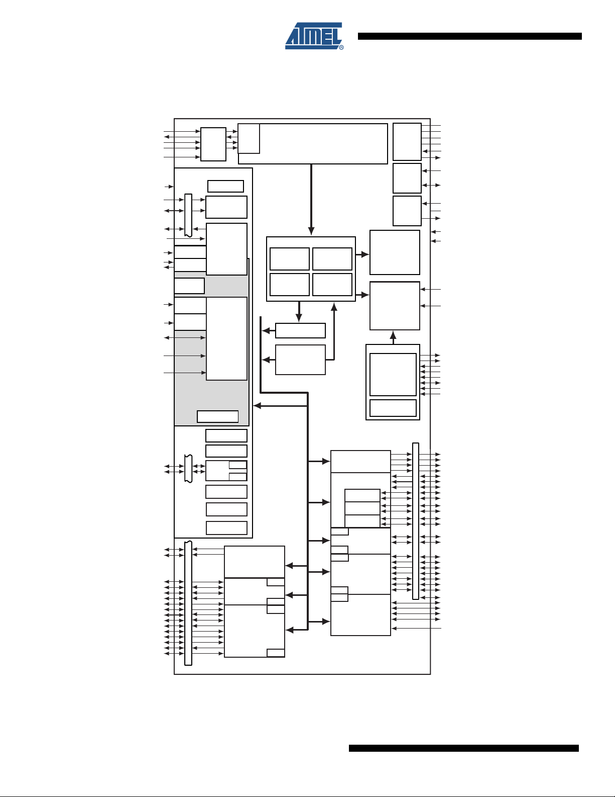
2. Block Diagram
Figure 2-1. AT91SAM7L128/64 Block Diagram
TDI
TDO
TMS
TCK
JTAGSEL
TST
FIQ
IRQ0-IRQ1
PCK0-PCK2
CLKIN
PLLRC
XIN
XOUT
VDDIO1
VDDIO1
NRST
NRSTB
FWUP
System Controller
PIO
PLL
OSC
32k RCOSC
BOD
POR
VDDIO1
JTAG
SCAN
2 MHz RCOSC
AIC
PMC
Supply
Controller
RTC
ICE
ARM7TDMI
Processor
Memory Controller
Embedded
Flash
Controller
Abort
Status
Peripheral Bridge
Peripheral Data
Controller
11 Channels
APB
Address
Decoder
Misalignment
Detection
Charge
Pump
LCD
Voltage
Regulator
1.8 V
Voltage
Regulator
SRAM
2 Kbytes( Back-up)
4 Kbytes (Core)
Flash
64/128 Kbytes
ROM
(12 Kbytes)
Fast Flash
Programming
Interface
SAM-BA
CAPP1
CAPM1
CAPP2
CAPM2
VDDINLCD
VDD3V6
VDDLCD
VDDIO2
VDDIO1
GND
VDDOUT
VDDCORE
VDDIO2
VDDCORE
ERASE
PGMRDY
PGMNVALID
PGMNOE
PGMCK
PGMM0-PGMM3
PGMD0-PGMD15
PGMNCMD
PGMEN0-PGMEN2
DRXD
DTXD
SEG00-SEG39
COM0-COM9
RXD0
TXD0
SCK0
RTS0
CTS0
RXD1
TXD1
SCK1
RTS1
CTS1
DCD1
DSR1
DTR1
RI1
PIO
PIO
PIT
WDT
PDC
DBGU
PDC
PIOA (26 IOs)
PIOB (24 IOs)
PIOC (30 IOs)
LCD Controller
USART0
USART1
PDC
PDC
PDC
PDC
Timer Counter
PDC
PDC
PDC
PDC
PDC
PWMC
TC0
TC1
TC2
TWI
SPI
ADC
PIO
PWM0
PWM1
PWM2
PWM3
TCLK0
TCLK1
TCLK2
TIOA0
TIOB0
TIOA1
TIOB1
TIOA2
TIOB2
TWD
TWCK
NPCS0
NPCS1
NPCS2
NPCS3
MISO
MOSI
SPCK
ADTRG
AD0
AD1
AD2
AD3
ADVREF
4
AT91SAM7L128/64 Preliminary
6257AS–ATARM–28-Feb-08
AT91SAM7L128/64 Preliminary
3. Signal Description
Table 3-1. Signal Description List
Active
Signal Name Function Type
Power
VDDIO1
VDDOUT Voltage Regulator Output Power
VDDCORE Core Power Supply Power Connected externally to VDDOUT
VDDINLCD Charge Pump Power Supply Power From 1.80V to 3.6V
VDD3V6 Charge Pump Output Power
VDDLCD LCD Voltage Regulator Power Supply Power
VDDIO2
CAPP1 Charge pump capacitor 1 Power
CAPM1 Charge pump capacitor 1 Power
CAPP2 Charge pump capacitor 2 Power
CAPM2 Charge pump capacitor 2 Power
FWUP Force Wake-up Input Low VDDIO1 Needs external Pull-up.
WKUP0-15
GND Ground Ground
XIN 32 kHz Oscillator Input Input VDDIO1
XOUT 32 kHz Oscillator Output Output VDDIO1
CLKIN Main Clock input Input VDDIO1 Should be tied low when not used.
PCK0 - PCK2 Programmable Clock Output Output
PLLRC PLL Filter Input VDDCORE
PLLRCGND PLL RC Filter Ground Power
TCK Test Clock Input VDDIO1 No internal pull-up resistor
TDI Test Data In Input VDDIO1 No internal pull-up resistor
TDO Test Data Out Output VDDIO1
TMS Test Mode Select Input VDDIO1 No internal pull-up resistor
JTAGSEL JTAG Selection Input VDDIO1 Internal Pull-down resistor
ERASE
I/O Lines (PIOC) and Voltage Regulator
Power Supply
LCD Voltage Regulator Output
and
LCD I/O Lines Power Supply (PIOA and
PIOB)
Wake-up inputs used in Backup mode and
Fast Start-up inputs in Wait mode
Clocks, Oscillators and PLLs
Flash and NVM Configuration Bits Erase
Command
Power From 1.80V to 3.6V
Power 1.80V to 3.6V
Input VDDIO1
ICE and JTAG
Flash Memory
Input High VDDIO1 Internal Pull-down (15 k
Level
Vol tag e
Reference Comments
Capacitor needed between CAPP1
and CAPM1.
Capacitor needed between CAPP2
and CAPM2.
Must not be connected to external
Ground.
Ω) resistor
6257AS–ATARM–28-Feb-08
5

Table 3-1. Signal Description List (Continued)
Active
Signal Name Function Type
Reset/Test
NRST Microcontroller Reset I/O Low VDDIO1 Internal Pull-up (100 kΩ) resistor
TST Test Mode Select Input High VDDIO1 Internal Pull-down (15 kΩ) resistor
NRSTB Asynchronous Master Reset Input Low VDDIO1 Internal Pull-up (15 k
Debug Unit
DRXD Debug Receive Data Input
DTXD Debug Transmit Data Output
AIC
IRQ0 - IRQ1 External Interrupt Inputs Input
FIQ Fast Interrupt Input Input
PIO
PA0 - PA25 Parallel IO Controller A I/O VDDIO2 Pulled-up input at reset
PB0 - PB23 Parallel IO Controller B I/O VDDIO2 Pulled-up input at reset
PC0 - PC29 Parallel IO Controller C I/O VDDIO1 Pulled-up input at reset
USART
SCK0 - SCK1 Serial Clock I/O
TXD0 - TXD1 Transmit Data I/O
RXD0 - RXD1 Receive Data Input
RTS0 - RTS1 Request To Send Output
CTS0 - CTS1 Clear To Send Input
DCD1 Data Carrier Detect Input
DTR1 Data Terminal Ready Output
DSR1 Data Set Ready Input
RI1 Ring Indicator Input
Timer/Counter
TCLK0 - TCLK2 External Clock Inputs Input
TIOA0 - TIOA2 Timer Counter I/O Line A I/O
TIOB0 - TIOB2 Timer Counter I/O Line B I/O
PWM Controller
PWM0 - PWM3 PWM Channels Output
Serial Peripheral Interface
MISO Master In Slave Out I/O
MOSI Master Out Slave In I/O
SPCK SPI Serial Clock I/O
NPCS0 SPI Peripheral Chip Select 0 I/O Low
NPCS1-NPCS3 SPI Peripheral Chip Select 1 to 3 Output Low
Level
Vol tag e
Reference Comments
Ω) resistor
6
AT91SAM7L128/64 Preliminary
6257AS–ATARM–28-Feb-08

AT91SAM7L128/64 Preliminary
Table 3-1. Signal Description List (Continued)
Active
Signal Name Function Type
Two-Wire Interface
TWD Two-wire Serial Data I/O
TWCK Two-wire Serial Clock I/O
Analog-to-Digital Converter
AD0-AD3 Analog Inputs Input VDDCORE
ADTRG ADC Trigger Input
ADVREF ADC Reference Analog VDDCORE
Fast Flash Programming Interface
PGMEN0PGMEN2
PGMM0PGMM3
PGMD0PGMD15
PGMRDY Programming Ready Output High VDDIO1
PGMNVALID Data Direction Output Low VDDIO1
PGMNOE Programming Read Input Low VDDIO1
PGMCK Programming Clock Input VDDIO1
PGMNCMD Programming Command Input Low VDDIO1
COM[9:0] Common Terminals Output VDDIO2
SEG[39:0] Segment Terminals Output VDDIO2
Programming Enabling Input VDDIO1
Programming Mode Input VDDIO1
Programming Data I/O VDDIO1
Segmented LCD Controller
Level
Vol tag e
Reference Comments
6257AS–ATARM–28-Feb-08
7

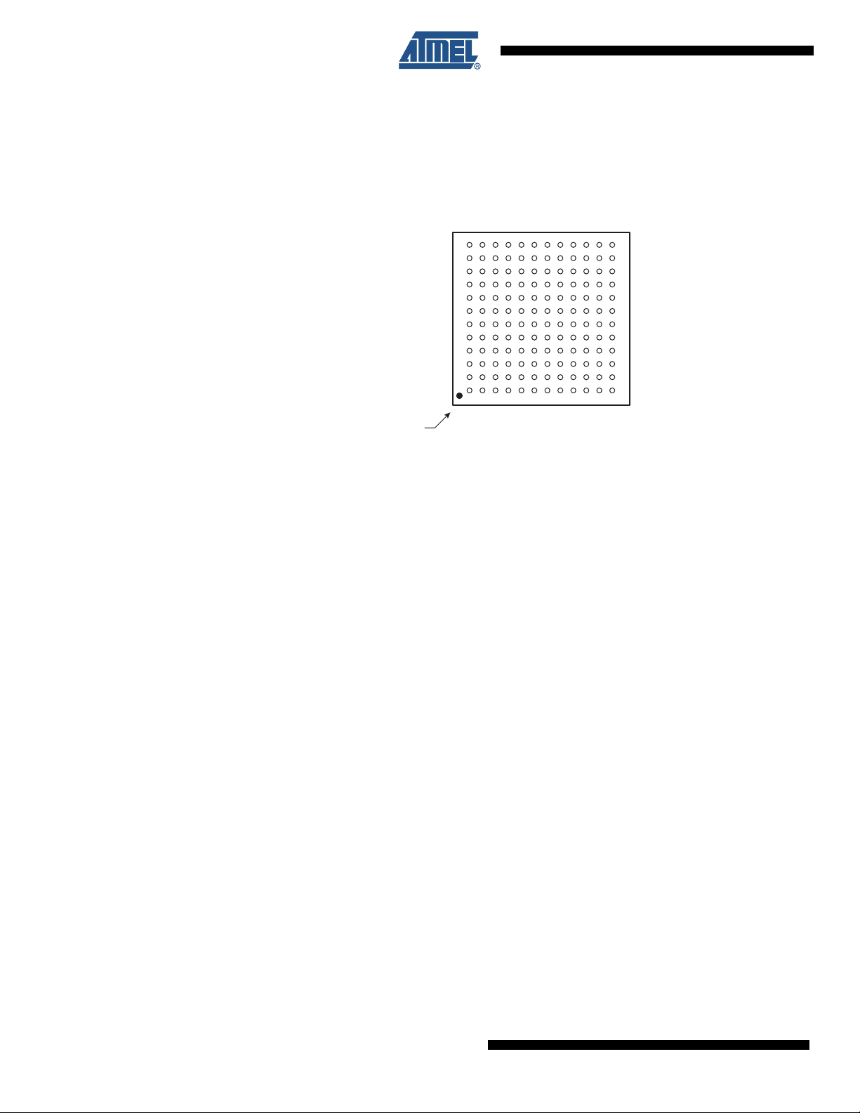
4. Package and Pinout
The AT91SAM7L128/64 is available in:
• 20 x 14 mm 128-lead LQFP package with a 0.5 mm lead-pitch
• 10 x 10 mm 144-ball LFBGA package with a 0.8 mm pitch.
The part is also available in die delivery.
4.1 128-lead LQFP Package Outline
Figure 4-1 shows the orientation of the 128-lead LQFP package.
A detailed mechanical description is given in the Mechanical Characteristics section of the product datasheet.
Figure 4-1. 128-lead LQFP Package Outline (Top View)
103
128
102
1
65
64
39
38
8
AT91SAM7L128/64 Preliminary
6257AS–ATARM–28-Feb-08
AT91SAM7L128/64 Preliminary
4.2 128-lead LQFP Package Pinout
Table 4-1. Pinout for 128-lead LQFP Package
1 TST 33 VDDLCD 65 PB21 97 PC10/PGMM3
2 VDDCORE 34 VDD3V6 66 PB22 98 PC11/PGMD0
3 PA0 35 CAPM2 67 PB23 99 PC12/PGMD1
4 PA1 36 CAPP2 68 GND 100 VDDCORE
5 PA2 37 CAPM1 69 ADVREF 101 PC13/PGMD2
6 PA3 38 CAPP1 70 AD3 102 PC14/PGMD3
7 PA4 39 VDDINLCD 71 AD2 103 PC15/PGMD4
8 PA5 40 GND 72 AD1 104 PC16/PGMD5
9 PA6 41 PB0 73 AD0 105 PC17/PGMD6
10 PA7 42 PB1 74 VDDOUT 106 PC18/PGMD7
11 PA8 43 PB2 75 VDDIO1 107 PC19/PGMD8
12 PA9 44 PB3 76 GND 108 PC20/PGMD9
13 PA10 45 PB4 77 PC28 109 PC21/PGMD10
14 GND 46 PB5 78 PC29 110 PC22/PGMD11
15 VDDIO2 47 PB6 79 NRST 111 PC23/PGMD12
16 PA11 48 PB7 80 ERASE 112 PC24/PGMD13
17 PA12 49 PB8 81 TCK 113 PC25/PGMD14
18 PA13 50 PB9 82 TMS 114 PC26/PGMD15
19 PA14 51 PB10 83 JTAGSEL 115 PC27
20 PA15 52 PB11 84 VDDCORE 116 TDI
21 PA16 53 PB12 85 VDDIO1 117 TDO
22 PA17 54 PB13 86 GND 118 FWUP
23 PA18 55 VDDIO2 87 PC0/PGMEN0 119 VDDIO1
24 PA19 56 GND 88 PC1/PGMEN1 120 GND
25 PA20 57 PB14 89 PC2/PGMEN2 121 PLLRC
26 PA21 58 PB15 90 PC3/PGMNCMD 122 PLLRCGND
27 PA22 59 PB16 91 PC4/PGMRDY 123 GND
28 VDDCORE 60 PB17 92 PC5/PGMNOE 124 VDDCORE
29 PA23 61 PB18 93 PC6/PGMNVALID 125 CLKIN
30 PA24 62 VDDCORE 94 PC7/PGMM0 126 NRSTB
31 PA25 63 PB19 95 PC8/PGMM1 127 XIN/PGMCK
32 VDDIO2 64 PB20 96 PC9/PGMM2 128 XOUT
6257AS–ATARM–28-Feb-08
9
4.3 144-ball LFBGA Package Outline
Figure 4-2 shows the orientation of the 144-ball LFBGA package.
A detailed mechanical description is given in the Mechanical Characteristics section of the product datasheet.
Figure 4-2. 144-ball LFBGA Package Outline (Top View)
Ball A1
12
11
10
9
8
7
6
5
4
3
2
1
ABCDEFGHJKLM
10
AT91SAM7L128/64 Preliminary
6257AS–ATARM–28-Feb-08

AT91SAM7L128/64 Preliminary
4.4 144-ball LFBGA Pinout
Table 4-2. SAM7L128/64 Pinout for 144-ball LFBGA Package
Pin Signal Name Pin Signal Name Pin Signal Name Pin Signal Name
A1 XOUT D1 PA6 G1 VDD3V6 K1 CAPM1
A2 XIN D2 PA5 G2 PA17 K2 VDDIO2
A3 VDDCORE D3 PA7 G3 PA16 K3 VDDIO2
A4 GND D4 NC G4 PA15 K4 PA25
A5 PLLRCGND D5 PC26/PGMD15 G5 GND K5 PB3
A6 PLLRC D6 PC25/PGMD14 G6 GND K6 PB10
A7 PC24/PGMD13 D7 PC21/PGMD11 G7 GND K7 PB13
A8 PC23//PGMD12 D8 PC18/PGMD7 G8 VDDIO1 K8 PB15
A9 PC17/PGMD6 D9 PC6/PGMNVALID G9 NRST K9 PB20
A10 NC D10 PC7/PGMM0 G10 TMS K10 VDDCORE
A11 PC14 D11 PC4/PGMRDY G11 ERASE K11 VDDCORE
A12 PC12 D12 PC3/PGMNCMD G12 VDDOUT K12 AD2
B1 PA1 E1 VDDIO2 H1 CAPM2 L1 CAPP1
B2 PA0 E2 PA10 H2 PA22 L2 VDDIO2
B3 NRSTB E3 PA9 H3 PA19 L3 VDDIO2
B4 TEST E4 PA11 H4 PA18 L4 PB4
B5 TDO E5 PA8 H5 GND L5 PB5
B6 PC27 E6 VDDIO1 H6 GND L6 PB11
B7 GND E7 VDDIO1 H7 GND L7 PB12
B8 NC E8 VDDIO1 H8 VDDCORE L8 PB17
B9 PC20/PGMD9 E9 PC5/PGMNOE H9 PC29 L9 PB19
B10 PC15/PGMD4 E10 PC0/PGMEN0 H10 VDDCORE L10 PB22
B11 PC13/PGMD2 E11 PC2/PGMEN2 H11 PC28 L11 PB23
B12 PC11/PGMD0 E12 VDDCORE H12 AD0 L12 AD3
C1 PA3 F1 VDDLCD J1 CAPP2 M1 VDDINLCD
C2 PA4 F2 PA13 J2 PA23 M2 PB0
C3 PA2 F3 PA14 J3 PA24 M3 PB1
C4 CLKIN F4 PA12 J4 PA21 M4 PB2
C5 FWUP F5 GND J5 PA20 M5 PB6
C6 TDI F6 GND J6 PB8 M6 PB7
C7 PC22/PGMD11 F7 GND J7 PB9 M7 VDDIO2
C8 PC19/PGMD8 F8 VDDIO1 J8 PB14 M8 PB16
C9 PC16/PGMD5 F9 TCK J9 VDDCORE M9 PB18
C10 PC9/PGMM2 F10 JTAGSEL J10 VDDCORE M10 PB21
C11 PC10/PGMM3 F11 PC1/PGMEN1 J11 VDDCORE M11 GND
C12 PC8/PGMM1 F12 VDDIO1 J12 AD1 M12 ADVREF
6257AS–ATARM–28-Feb-08
11

5. Power Considerations
5.1 Power Supplies
The AT91SAM7L128/64 has six types of power supply pins and integrates a voltage regulator,
allowing the device to be supplied with only one voltage. The six power supply pin types are:
• VDDOUT pin. It is the output of the voltage regulator. Output voltage can be programmed
from 1.55V to 1.80V by steps of 100 mV.
• VDDIO1 pin. It powers the voltage regulator input and all the PIOC IO lines (1.8V-3.6V).
VDDIO1 voltage must be above 2.2V to allow the chip to start-up (POR threshold).
• VDDIO2 pin. It powers the PIOA and PIOB I/O lines (1.8V-3.6V). It is also the output of the
LCD voltage regulator. The output voltage can be programmed from 2.4V to 3.4V with 16
steps.
• VDDCORE pin. It powers the logic of the device, the PLL, the 2 MHz Fast RC oscillator, the
ADC and the Flash memory. It must be connected to the VDDOUT pin with a decoupling
capacitor.
• VDDINLCD pin. It powers the charge pump which can be used as LCD Regulator power
supply. Voltage ranges from 1.8V to 3.6V.
No separate ground pins are provided for the different power supplies. Only GND pins are provided and should be connected as shortly as possible to the system ground plane.
5.2 Low Power Modes
The various low power modes of the AT91SAM7L128/64 are described below.
5.2.1 Off (Power Down) Mode
In off (power down) mode, the entire chip is shut down. Only a low level on the FWUP pin can
wake up the AT91SAM7L128/64 (by a push-button for example). Internally, except for the
FWUP pin through VDDIO1, none of the chip is supplied.
Once the internal main power switch has been activated by FWUP, the 32 kHz RC oscillator and
the Supply Controller are supplied, then the core and peripherals are reset and the
AT91SAM7L128/64 enters in active mode. Refer to the System Controller Block Diagram, Fig-
ure 9-1 on page 30.
At first power-up, if FWUP is tied high, the device enters off mode. The PIOA and PIOB pins’
states are undefined. PIOC and NRST pins are initialized as high impedance inputs.
Once the device enters active mode, the core and the parallel input/output controller are reset.
Then, if the chip enters off mode, PIOA and PIOB pins are configured as inputs with pull-ups and
PIOC pins as high impedance inputs.
Current consumption in this mode is typically 100 nA.
5.2.2 Backup Mode
In backup mode, the supply controller, the zero-power power-on reset and the 32 kHz oscillator
(software selectable internal RC or external crystal) remain running. The voltage regulator and
the core are switched off.
Prior to entering this mode, the RTC, the backup SRAM, the brownout detector, the charge
pump, the LCD voltage regulator and the LCD controller can be set on or off separately.
12
AT91SAM7L128/64 Preliminary
6257AS–ATARM–28-Feb-08

5.2.3 Wait Mode
5.2.4 Idle Mode
5.2.5 Active Mode
AT91SAM7L128/64 Preliminary
Table 5-1 on page 13 shows an example of backup mode with backup SRAM and RTC running.
When entering this mode, all PIO pins keep their previous states, they are reinitialized as inputs
with pull-ups at wake-up.
The AT91SAM7L128/64 can be awakened from this mode through the FWUP pin, an event on
WUP0-15 pins, or an RTC alarm or brownout event.
Current consumption is 3.5 µA typical without the LCD controller running.
In wait mode, the voltage regulator must be set in deep mode. Voltage regulator output voltage
should be set at a minimum voltage to decrease leakage in the digital core. No clock is running
in the core. From this mode, a fast start-up is available (refer to Section 5.4 ”Fast Start-Up”).
In this mode, all PIO pins keep their previous states.
The processor is in idle mode which means that the processor has no clock but the Master clock
(MCK) remains running. The processor can also be wakened by an IRQ or FIQ.
The total dynamic power consumption is less than 30 mA at full speed (36 MHz) when running
out of the Flash. The power management controller can be used to adapt the frequency and the
regulator output voltage can be adjusted to optimize power consumption.
5.2.6 Low Power Mode Summary Table
The modes detailed above are the main modes. In off mode, no options are available but once
the shutdown controller is set to on, each part can be set to on, or off, separately and more
modes can be active. The table below shows a summary of the configurations of the low power
modes.
Table 5-1. Low Power Mode Configuration Summary
SUPC,
32 kHz
Oscillator,
Mode FWUP
Off Mode X FWUP pin 100 nA typ < 5 ms
Backup Mode
(with SRAM and
RTC)
Wait Mode (with
SRAM and RTC)
Idle Mode X X X X X
XXXX
XXXX XX
POR RTC
Notes: 1. When considering wake-up time, the time required to start the PLL is not taken into account. Once started, the
AT91SAM7128/L64 works with the 2 MHz Fast RC oscillator. The user has to add the PLL start-up time if it is needed in the
system. The wake-up time is defined as the time taken for wake up until the first instruction is fetched.
2. The external LCD current consumption and the external loads on PIOs are not taken into account in the calculation.
3. BOD current consumption is not included.
4. Depends on MCK frequency.
Backup
SRAM
Regulator
(Deep Mode) Core
Potential Wake-up
Sources Consumption
FWUP pin
WUP0-15 pins
BOD alarm
RTC alarm
Fast start-up through
WUP0-15 pins
IRQs
FIQ
(2)(3)
Wake-up Time
3.5 µA typ < 0.5 ms
9 µA typ
(4) (4)
< 2 µs (in case of
fast start-up)
(1)
6257AS–ATARM–28-Feb-08
13
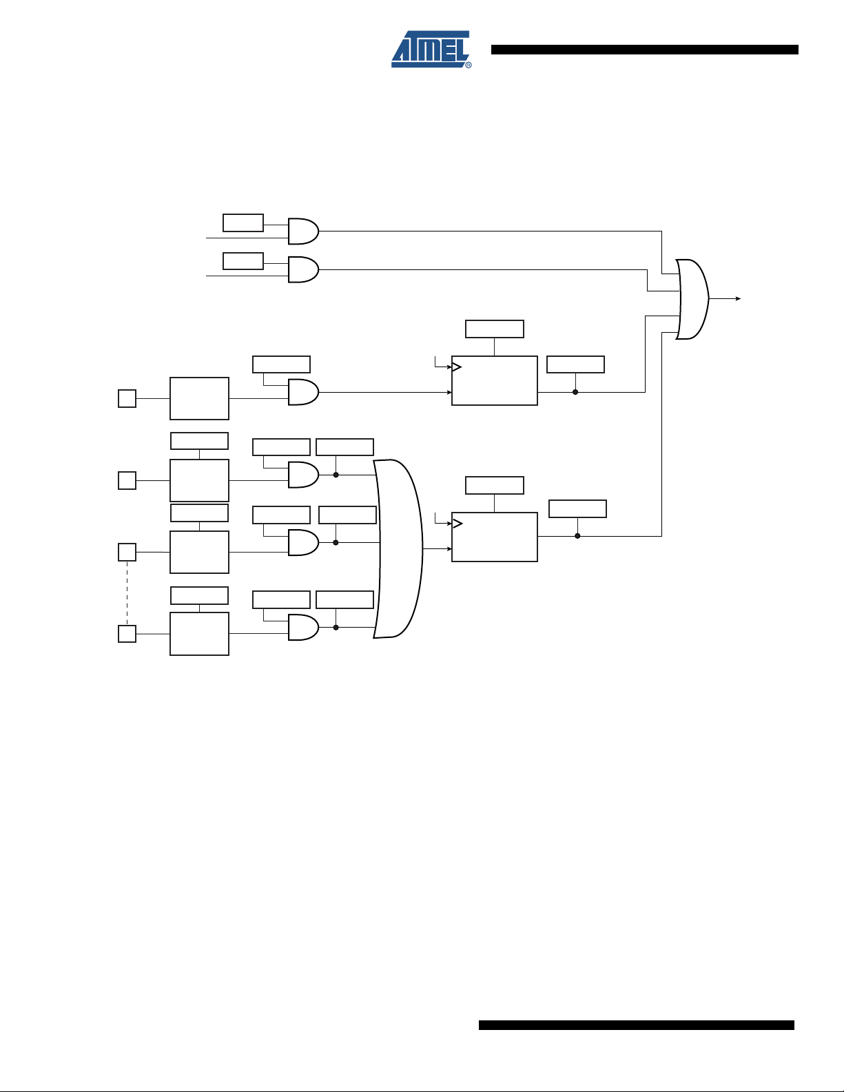
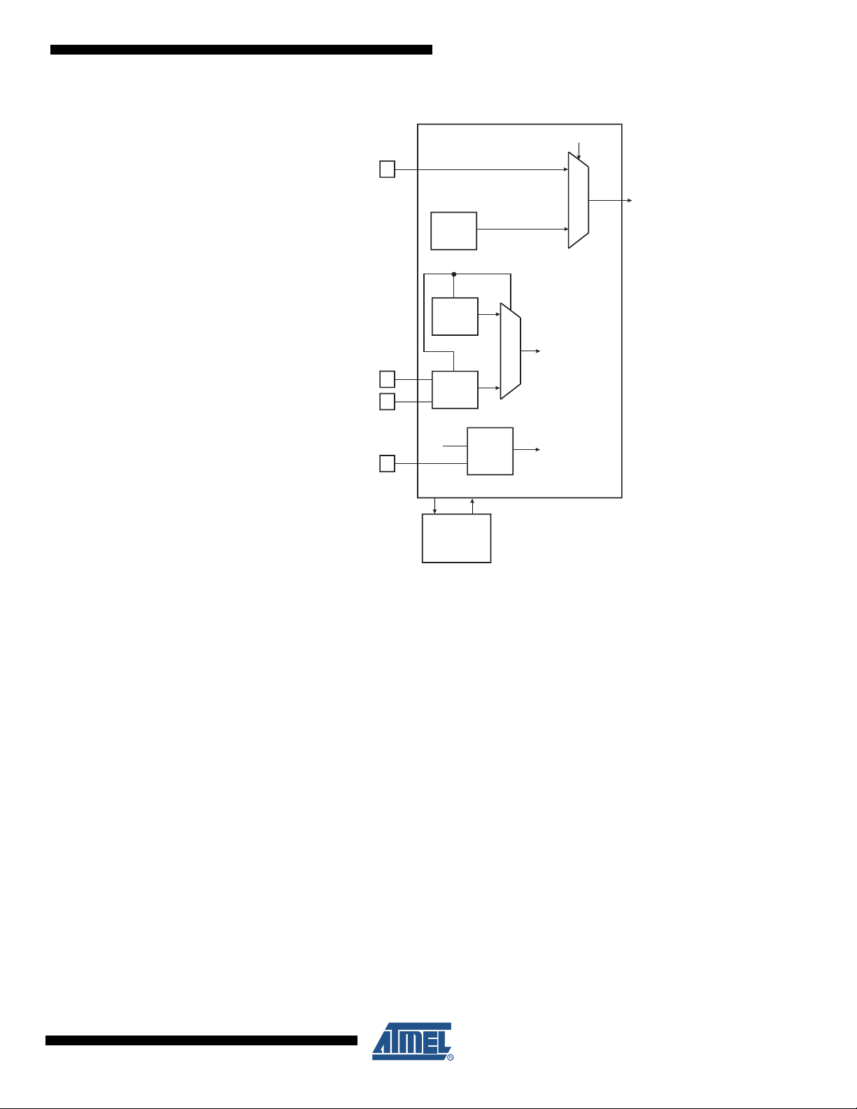
5.3 Wake-up Sources
The wake-up events allow the device to exit from backup mode. When a wake-up event is
detected, the supply controller performs a sequence which automatically reenables the voltage
regulator and the backup SRAM power supply, if it is not already enabled.
Figure 5-1. Wake Up Sources
FWUP
WKUP0
WKUP1
WKUP15
brown_out
rtc_alarm
Falling
Edge
Detector
WKUPT0
Falling/Rising
Edge
Detector
WKUPT1
Falling/Rising
Edge
Detector
WKUPT15
Falling/Rising
Edge
Detector
BODEN
RTCEN
FWUPDBC
FWUPEN FWUP
WKUPEN0
WKUPEN1
WKUPEN15
WKUPIS0
WKUPIS1
WKUPIS15
SLCK
Debouncer
WKUPDBC
SLCK
Debouncer
Core
Supply
Restart
WKUPS
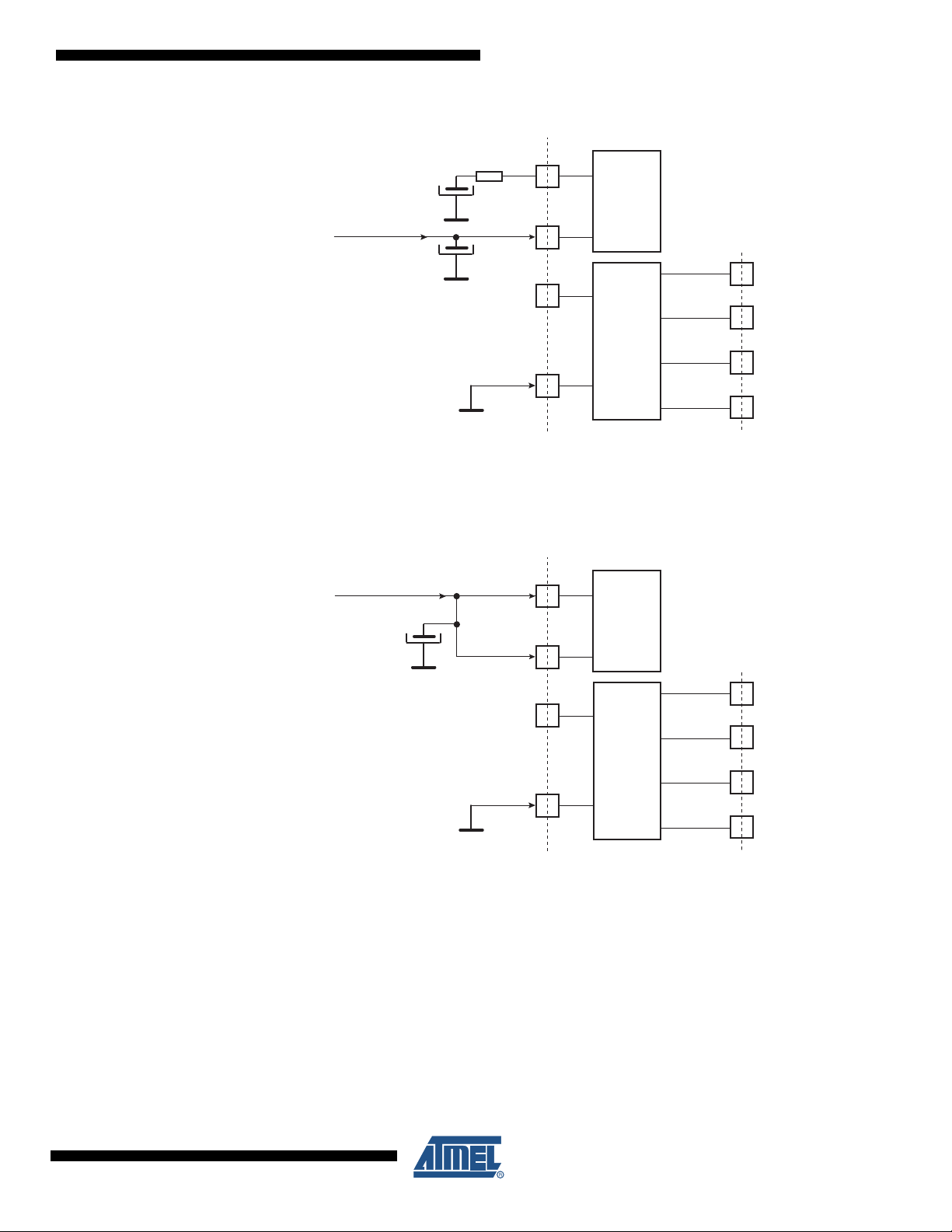
5.4 Fast Start-Up
14
AT91SAM7L128/64 Preliminary
The SAM7L128/64 allows the processor to restart in a few microseconds while the processor is
in wait mode. A fast start up can occur upon detection of a low level on one of the 16 wake-up
inputs.
The fast restart circuitry, as shown in Figure 5-2, is fully asynchronous and provides a fast startup signal to the power management controller. As soon as the fast start-up signal is asserted,
the PMC automatically restarts the embedded 2 MHz Fast RC oscillator, switches the master
clock on this 2 MHz clock and reenables the processor clock, if it is disabled.
6257AS–ATARM–28-Feb-08

Figure 5-2. Fast Start-Up Circuitry
FSTT0
WKUP0
FSTT1
AT91SAM7L128/64 Preliminary
5.5 Voltage Regulator
The AT91SAM7L128/64 embeds a voltage regulator that is managed by the supply controller.
This internal regulator is only intended to supply the internal core of AT91SAM7L128/64. It features three different operating modes:
• In normal mode, the voltage regulator consumes less than 30 µA static current and draws
• In deep mode, the current consumption of the voltage regulator is less than 8.5 µA. It can
• In shutdown mode, the voltage regulator consumes less than 1 µA while its output is driven
Furthermore, in normal and deep modes, the regulator output voltage can be programmed by
software with 4 different steps within the range of 1.55V to 1.80V. The default output voltage is
1.80V in both normal and deep modes. The voltage regulator can regulate 1.80V output voltage
as long as the input voltage is above 1.95V. Below 1.95V input voltage, the output voltage
remains above 1.65V.
WKUP1
FSTT15
WKUP15
fast_restart
60 mA of output current.
draw up to 1 mA of output current. The default output voltage is 1.80V and the start-up time to
reach normal mode is inferior to 400 µs.
internally to GND. The default output voltage is 1.80V and the start-up time to reach normal
mode is inferior to 400 µs.
6257AS–ATARM–28-Feb-08
Output voltage adjusting ability allows current consumption reduction on VDDCORE and also
enables programming a lower voltage when the input voltage is lower than 1.95V.
At 1.55V, the Flash is still functional but with slower read access time. Programming or erasing
the Flash is not possible under these conditions. MCK maximum frequency is 25 MHz with
VDDCORE at 1.55V (1.45V minimum).
The regulator has an indicator that can be used by the software to show that the output voltage
has the correct value (output voltage has reached at least 80% of the typical voltage). This flag
is used by the supply controller. This feature is only possible when the voltage regulator is in
normal mode at 1.80V.
Adequate output supply decoupling is mandatory for VDDOUT in order to reduce ripple and
avoid oscillations. One external 2.2 µF (or 3.3 µF) X7R capacitor must be connected between
VDDOUT and GND.
15

Adequate input supply decoupling is mandatory for VDDIO1 in order to improve startup stability
and reduce source voltage drop. The input decoupling capacitor should be placed close to the
chip. For example, two capacitors can be used in parallel, 100 nF NPO and 4.7 µF X7R.
5.6 LCD Power Supply
The AT91SAM7L128/64 embeds an on-chip LCD power supply comprising a regulated charge
pump and an adjustable voltage regulator.
The regulated charge pump output delivers 3.6V as long as its input is supplied between 1.8V
and 3.6V. The regulated charge pump only requires two external flying capacitors and one external tank capacitor to operate.
Adequate input supply decoupling is mandatory for VDDINLCD in order to improve startup stability and reduce source voltage drop. The input decoupling capacitor should be placed close to
the chip.
Current consumption of the charge pump and LCD bias when active is 350 µA (max case).
The regulated charge pump can be used to supply the LCD voltage regulator or as a 3.6V voltage reference delivering up to 4 mA.
The LCD voltage regulator output voltage is software selectable from 2.4V to 3.4V with 16 levels. Its input should be supplied in the range of 2.5 to 3.6V. The LCD voltage regulator can be
supplied by the regulated charge pump output or by an external supply.
When the LCD voltage regulator is not used, its output must be connected to an external source
in order to supply the PIOA and PIOB I/O lines.
Figure 5-3 below shows the typical schematics needed:
Figure 5-3. The Charge Pump Supplies the LCD Regulator
R = 10Ω
External supply
VDDIO2
VDDLCD
VDD3V6
VDDINLCD
LCD
Voltage
Regulator
Charge
Pump
CAPP1
CAPM1
CAPP2
CAPM2
16
AT91SAM7L128/64 Preliminary
6257AS–ATARM–28-Feb-08
AT91SAM7L128/64 Preliminary
Figure 5-4. The LCD Regulator is Externally Supplied
R = 10Ω
External supply
VDDIO2
VDDLCD
VDD3V6
VDDINLCD
LCD
Voltage
Regulator
Charge
Pump
CAPP1
CAPM1
CAPP2
CAPM2
If the charge pump is not needed, the user can apply an external voltage. See Figure 5-5 below:
Figure 5-5. The Charge Pump and the LCD Regulator are Not Used
External supply
VDDIO2
VDDLCD
LCD
Voltage
Regulator
CAPP1
VDD3V6
CAPM1
Charge
Pump
VDDINLCD
CAPP2
CAPM2
Please note that in this topology, switching time enhancement buffers are not available. (Refer
Section 10.13 ”Segment LCD Controller”.)
6257AS–ATARM–28-Feb-08
17

5.7 Typical Powering Schematics
The AT91SAM7L128/64 supports a 1.8V-3.6V single supply mode. The internal regulator input
connected to the source and its output feeds VDDCORE. Figure 5-6 shows the power schemat-
ics to be used.
Figure 5-6. 3.3V System Single Power Supply Schematic
R = 10Ω
Main Supply (1.8V-3.6V)
VDDIO2
VDDLCD
VDD3V6
VDDINLCD
VDDIO1
VDDOUT
VDDCORE
LCD
Voltage
Regulator
Charge
Pump
Voltage
Regulator
CAPP1
CAPM1
CAPP2
CAPM2
18
AT91SAM7L128/64 Preliminary
6257AS–ATARM–28-Feb-08

6. I/O Line Considerations
6.1 JTAG Port Pins
TMS, TDI and TCK are schmitt trigger inputs. TMS, TDI and TCK do not integrate a pull-up
resistor.
TDO is an output, driven at up to VDDIO, and has no pull-up resistor.
The JTAGSEL pin is used to select the JTAG boundary scan when asserted at a high level. The
JTAGSEL pin integrates a permanent pull-down resistor of about 15 kΩ to GND, so that it can be
left unconnected for normal operations.
6.2 Test Pin
The TST pin is used for manufacturing test or fast programming mode of the AT91SAM7L128/64
when asserted high. The TST pin integrates a permanent pull-down resistor of about 15 kΩ to
GND, so that it can be left unconnected for normal operations.
To enter fast programming mode, the TST and CLKIN pins must be tied high while FWUP is tied
low.
AT91SAM7L128/64 Preliminary
6.3 NRST Pin
6.4 NRSTB Pin
6.5 ERASE Pin
The NRST pin is bidirectional. It is handled by the on-chip reset controller and can be driven low
to provide a reset signal to the external components or asserted low externally to reset the
microcontroller. There is no constraint on the length of the reset pulse and the reset controller
can guarantee a minimum pulse length.
The NRST pin integrates a permanent pull-up resistor to VDDIO1 of about 100 kΩ.
The NRSTB pin is input only and enables asynchronous reset of the AT91SAM7L128/64 when
asserted low. The NRSTB pin integrates a permanent pull-up resistor of about 15 kΩ. This
allows connection of a simple push button on the NRBST pin as a system-user reset.
In all modes, this pin will reset the chip. It can be used as an external system reset source.
In harsh environments, it is recommended to add an external capacitor (10 nF) between NRSTB
and VDDIO1.
NRSTB pin must not be connected to VDDIO1. There must not be an external pull-up on
NRSTB.
The ERASE pin is used to reinitialize the Flash content and some of its NVM bits. It integrates a
permanent pull-down resistor of about 15 kΩ to GND, so that it can be left unconnected for nor-
mal operations.
6257AS–ATARM–28-Feb-08
This pin is debounced by SCLK to improve the glitch tolerance. When the ERASE pin is tied high
during less than 100 ms, it is not taken into account. The pin must be tied high during more than
220 ms to perform the reinitialization of the Flash.
19

6.6 PIO Controller Lines
All the I/O lines; PA0 to PA25, PB0 to PB23, PC0 to PC29 integrate a programmable pull-up
resistor. Programming of this pull-up resistor is performed independently for each I/O line
through the PIO controllers. All I/Os have input schmitt triggers.
Typical pull-up value is 100 kΩ.
Maximum frequency is:
• 36 MHz under 25 pF of load on PIOC
• 36 MHz under 25 pF of load on PIOA and PIOB
6.7 I/O Line Current Drawing
The PIO lines PC5 to PC8 are high-drive current capable. Each of these I/O lines can drive up to
4 mA permanently. The remaining I/O lines can draw only 2 mA.
Each I/O is designed to achieve very small leakage. However, the total current drawn by all the
I/O lines cannot exceed 150 mA.
20
AT91SAM7L128/64 Preliminary
6257AS–ATARM–28-Feb-08

7. Processor and Architecture
7.1 ARM7TDMI Processor
• RISC processor based on ARMv4T Von Neumann Architecture
– Runs at up to 36 MHz, providing 0.9 MIPS/MHz
• Two instruction sets
–ARM
– Thumb high code density 16-bit instruction set
• Three-stage pipeline architecture
– Instruction Fetch (F)
– Instruction
– Execute (E)
7.2 Debug and Test Features
• Integrated embedded in-circuit emulator
– Two watchpoint units
– Test access port accessible through a JTAG protocol
– Debug communication channel
• Debug Unit
–Two-pin UART
– Debug communication channel interrupt handling
– Chip ID Register
• IEEE1149.1 JTAG Boundary-scan on all digital pins
®
high-performance 32-bit instruction set
Decode (D)
AT91SAM7L128/64 Preliminary
7.3 Memory Controller
• Programmable Bus Arbiter
• Address decoder provides selection signals for
• Abort Status Registers
• Misalignment Detector
• Remap Command
• Enhanced Embedded Flash Controller
– Handles requests from the ARM7TDMI and the Peripheral DMA Controller
– Five internal 1 Mbyte memory areas
– One 256 Mbyte embedded peripheral area
– Source, Type and all parameters of the access leading to an abort are saved
– Facilitates debug by detection of bad pointers
– Alignment checking of all data accesses
– Abort generation in case of misalignment
– Remaps the SRAM in place of the embedded non-volatile memory
– Allows handling of dynamic exception vectors
– Peripheral protection against write and/or user access
6257AS–ATARM–28-Feb-08
21

– Embedded Flash interface, up to three programmable wait states
– Prefetch buffer, buffering and anticipating the 16-bit requests, reducing the required
wait states
– Key-protected program, erase and lock/unlock sequencer
– Single command for erasing, programming and locking operations
– Interrupt generation in case of forbidden operation
7.4 Peripheral DMA Controller
• Handles data transfer between peripherals and memories
• Eleven channels
– Two for each USART
– Two for the Debug Unit
– Two for the Serial Peripheral Interface
– Two for the Two Wire Interface
– One for the Analog-to-digital Converter
• Low bus arbitration overhead
– One Master Clock cycle needed for a transfer from memory to peripheral
– Two Master Clock cycles needed for a transfer from peripheral to memory
• Next Pointer management for reducing interrupt latency requirements
22
AT91SAM7L128/64 Preliminary
6257AS–ATARM–28-Feb-08

8. Memories
AT91SAM7L128/64 Preliminary
• 128 Kbytes of Flash Memory (AT91SAM7L128)
– Single plane
– One bank of 512 pages of 256 bytes
– Fast access time, 15 MHz single-cycle access in Worst Case conditions
– Page programming time: 4.6 ms, including page auto-erase
– Page programming without auto-erase: 2.3 ms
– Full chip erase time: 10 ms
– 10,000 write cycles, 10-year data retention capability
– 16 lock bits, each protecting 16 lock regions of 32 pages
– Protection Mode to secure contents of the Flash
• 64 Kbytes of Flash Memory (AT91SAM7L64)
– Single plane
– One bank of 256 pages of 256 bytes
– Fast access time, 15 MHz single-cycle access in Worst Case conditions
– Page programming time: 4.6 ms, including page auto-erase
– Page programming without auto-erase: 2.3 ms
– Full chip erase time: 10 ms
– 10,000 write cycles, 10-year data retention capability
– 8 lock bits, each protecting 8 lock regions of 32 pages
– Protection Mode to secure contents of the Flash
• 6 Kbytes of Fast SRAM
– Single-cycle access at full speed
– 2 Kbytes of Backup SRAM
– 4 Kbytes of Core SRAM
6257AS–ATARM–28-Feb-08
23

Figure 8-1. Memory Mapping
Address Memory Space
0x0000 0000
Internal Memories
0x0FFF FFFF
0x1000 0000
Undefined
(Abort)
0xEFFF FFFF
0xF000 0000
Internal Peripherals
0xFFFF FFFF
256 MBytes
14 x 256 MBytes
3,584 MBytes
256M Bytes
0x0000 0000
0x000F FFFF
0x0010 0000
0x001F FFFF
0x0020 0000
0x002F FFFF
0x0030 0000
0x003F FFFF
0x0040 0000
0x004F FFFF
0x0050 0000
0x0FFF FFFF
0xF000 0000
0xFFF9 FFFF
0xFFFA 0000
0xFFFA 3FFF
0xFFFA 4000
0xFFFB 3FFF
0xFFFB 4000
0xFFFB 7FFF
0xFFFB 8000
0xFFFB BFFF
0xFFFB C000
0xFFFB FFFF
0xFFFC 0000
0xFFFC 3FFF
0xFFFC 4000
0xFFFC 7FFF
0xFFFC 8000
0xFFFC BFFF
0xFFFC C000
0xFFFC FFFF
0xFFFD 0000
0xFFFD 7FFF
0xFFFD 8000
0xFFFD BFFF
0xFFFD C000
0xFFFD FFFF
0xFFFE 0000
0xFFFE 3FFF
0xFFFE 4000
0xFFFF EFFF
0xFFFF F000
0xFFFF FFFF
Internal Memory Mapping
Boot Memory (1)
Flash before Remap
SRAM after Remap
Internal Flash
Internal SRAM
(Core) 4 kbytes
Internal SRAM
(Back-up) 2 kbytes
Internal ROM
Reserved
Peripheral Mapping
Reserved
TC0, TC1, TC2
Reserved
SLCDC
TWI
Reserved
USART0
USART1
Reserved
PWMC
Reserved
ADC
Reserved
SPI
Reserved
SYSC
16 Kbytes
16 Kbytes
16 Kbytes
16 Kbytes
16 Kbytes
16 Kbytes
16 Kbytes
16 Kbytes
1 MBytes
1 MBytes
1 MBytes
253 MBytes
Note:
(1) Can be ROM, Flash or SRAM
depending on GPNVM1 and REMAP
System Controller Mapping
0xFFFF F000
AIC
0xFFFF F1FF
0xFFFF F200
DBGU
0xFFFF F3FF
0xFFFF F400
0xFFFF F5FF
0xFFFF F600
0xFFFF F7FF
0xFFFF F800
0xFFFF F9FF
0xFFFF FA00
0xFFFF FBFF
0xFFFF FC00
0xFFFF FCFF
0xFFFF FD00
0xFFFF FD0F
0xFFFF FD10
0xFFFF FD2F
0xFFFF FD30
0xFFFF FD3F
0xFFFF FD40
0xFFFF FD4F
0xFFFF FD50
0xFFFF FD5F
0xFFFF FD60
0xFFFF FD7F
0xFFFF FD80
0xFFFF FEFF
0xFFFF FF00
0xFFFF FFFF
PIOA
PIOB
PIOC
Reserved
PMC
RSTC
SUPC
Reserved
PIT
WDT
RTC
Reserved
MC
512 Bytes/
128 registers
512 Bytes/
128 registers
512 Bytes/
128 registers
512 Bytes/
128 registers
512 Bytes/
128 registers
256 Bytes/
64 registers
16 Bytes/
4 registers
32 Bytes/
8 registers
16 Bytes/
4 registers
16 Bytes/
4 registers
32 Bytes/
8 registers
256 Bytes/
64 registers
24
AT91SAM7L128/64 Preliminary
6257AS–ATARM–28-Feb-08

8.1 Embedded Memories
8.1.1 Internal Memories
8.1.1.1 Internal SRAM
The AT91SAM7L128/64 embeds a high-speed 4-Kbyte SRAM bank and a 2-Kbyte backup
SRAM bank. The backup SRAM is directly supplied on 1.8V-3.6V supply domain.
The 4-Kbyte Core SRAM is supplied by VDDCORE which is connected to the output of the voltage regulator.
After reset and until the Remap Command is performed, the 4-Kbyte Core SRAM is only accessible at address 0x0020 0000. The 2-Kbyte Backup SRAM is accessible at address 0x0030
0000.
After remap, the 4-Kbyte Core SRAM also becomes available at address 0x0.
The user can see the 6 Kbytes of SRAM contiguously at address 0x002F F000.
8.1.1.2 Internal ROM
The AT91SAM7L128/64 embeds an Internal ROM. The ROM is always mapped at address
0x0040 0000. The ROM contains the FFPI and SAM-BA program.
AT91SAM7L128/64 Preliminary
8.1.1.3 Internal Flash
ROM size is 12 Kbytes.
• The AT91SAM7L128 features one bank of 128 Kbytes of Flash.
• The AT91SAM7L64 features one bank of 64 Kbytes of Flash.
At any time, the Flash is mapped to address 0x0010 0000.
A general purpose NVM (GPNVM1) bit is used to boot either on the ROM (default) or from the
Flash.
This GPNVM1 bit can be cleared or set respectively through the commands “Clear General-purpose NVM Bit” and “Set General-purpose NVM Bit” of the EEFC User Interface.
Setting the GPNVM Bit 1 selects the boot from the Flash, clearing it selects the boot from the
ROM. Asserting ERASE clears the GPNVM Bit 1 and thus selects the boot from the ROM by
default.
6257AS–ATARM–28-Feb-08
25
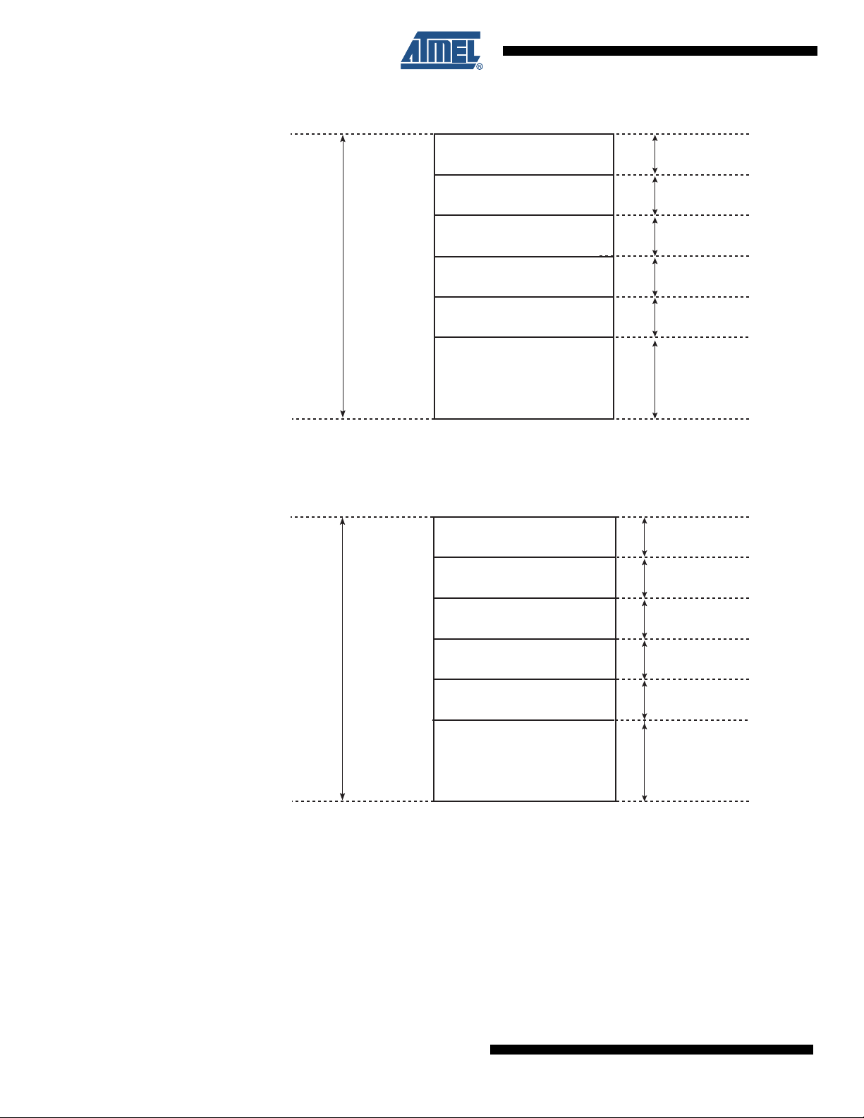
Figure 8-2. Internal Memory Mapping with GPNVM Bit 1 = 0 (default)
256 Mbytes
0x0000 0000
0x000F FFFF
0x0010 0000
0x001F FFFF
0x0020 0000
0x002F FFFF
0x0030 0000
0x003F FFFF
0x0040 0000
0x004F FFFF
0x0050 0000
0x0FFF FFFF
ROM Before Remap
Core SRAM (4 Kbytes) After Remap
Internal FLASH
Internal SRAM (Core)
4 Kbytes
Internal SRAM (Backup)
2 Kbytes
Internal ROM
12 Kbytes
Undefined Areas
(Abort)
Figure 8-3. Internal Memory Mapping with GPNVM Bit 1 = 1
256 Mbytes
0x0000 0000
0x000F FFFF
0x0010 0000
0x001F FFFF
0x0020 0000
0x002F FFFF
0x0030 0000
0x003F FFFF
0x0040 0000
0x004F FFFF
0x0050 0000
Flash Before Remap
Core SRAM (4 Kbytes) After Remap
Internal FLASH
Internal SRAM (Core)
4 Kbytes
Internal SRAM (Backup)
2 Kbytes
Internal ROM
12 Kbytes
Undefined Areas
(Abort)
1 Mbyte
1 Mbyte
1 Mbyte
1 Mbyte
1 Mbyte
251 Mbytes
1 Mbyte
1 Mbyte
1 Mbyte
1 Mbyte
1 Mbyte
251 Mbytes
8.1.2 Embedded Flash
8.1.2.1 Flash Overview
• The Flash of the AT91SAM7L128 is organized in 512 pages (single plane) of 256 bytes.
• The Flash of the AT91SAM7L64 is organized in 256 pages (single plane) of 256 bytes.
The Flash contains a 128-byte write buffer, accessible through a 32-bit interface.
8.1.2.2 Flash Power Supply
The Flash is supplied by VDDCORE through a power switch controlled by the Supply Controller.
26
AT91SAM7L128/64 Preliminary
0x0FFF FFFF
6257AS–ATARM–28-Feb-08

8.1.2.3 Enhanced Embedded Flash Controller
The Enhanced Embedded Flash Controller (EEFC) manages accesses performed by the masters of the system. It enables reading the Flash and writing the write buffer. It also contains a
User Interface, mapped within the Memory Controller on the APB.
The Enhanced Embedded Flash Controller ensures the interface of the Flash block with the 32bit internal bus. Its 128-bit wide memory interface increases performance. It also manages the
programming, erasing, locking and unlocking sequences of the Flash using a full set of commands. One of the commands returns the embedded Flash descriptor definition that informs the
system about the Flash organization, thus making the software generic.
8.1.2.4 Lock Regions
The AT91SAM7L128 Embedded Flash Controller manages 16 lock bits to protect 16 regions of
the flash against inadvertent flash erasing or programming commands. The AT91SAM7L128
contains 16 lock regions and each lock region contains 32 pages of 256 bytes. Each lock region
has a size of 8 Kbytes.
The AT91SAM7L64 Embedded Flash Controller manages 8 lock bits to protect 8 regions of the
flash against inadvertent flash erasing or programming commands. The AT91SAM7L64 contains 8 lock regions and each lock region contains 32 pages of 256 bytes. Each lock region has
a size of 8 Kbytes.
AT91SAM7L128/64 Preliminary
If a locked-region’s erase or program command occurs, the command is aborted and the EEFC
triggers an interrupt.
The 16 NVM bits are software programmable through the EEFC User Interface. The command
“Set Lock Bit” enables the protection. The command “Clear Lock Bit” unlocks the lock region.
Asserting the ERASE pin clears the lock bits, thus unlocking the entire Flash.
8.1.2.5 Security Bit Feature
The AT91SAM7L128/64 features a security bit, based on a specific General Purpose NVM bit
(GPNVM bit 0). When the security is enabled, any access to the Flash, either through the ICE
interface or through the Fast Flash Programming Interface, is forbidden. This ensures the confidentiality of the code programmed in the Flash.
This security bit can only be enabled, through the command “Set General Purpose NVM Bit 0” of
the EEFC User Interface. Disabling the security bit can only be achieved by asserting the
ERASE pin at 1, and after a full Flash erase is performed. When the security bit is deactivated,
all accesses to the Flash are permitted.
It is important to note that the assertion of the ERASE pin should always be longer than 200 ms.
As the ERASE pin integrates a permanent pull-down, it can be left unconnected during normal
operation. However, it is safer to connect it directly to GND for the final application.
8.1.2.6 Calibration Bits
NVM bits are used to calibrate the brownout detector and the voltage regulator. These bits are
factory configured and cannot be changed by the user. The ERASE pin has no effect on the calibration bits.
6257AS–ATARM–28-Feb-08
27

8.1.2.7 GPNVM Bits
The AT91SAM7L128/64 features two GPNVM bits that can be cleared or set respectively
through the commands “Clear GPNVM Bit” and “Set GPNVM Bit” of the EEFC User Interface..
Table 8-1. General-purpose Non-volatile Memory Bits
GPNVMBit[#] Function
0 Security bit
1 Boot mode selection
8.1.3 Fast Flash Programming Interface
The Fast Flash Programming Interface allows programming the device through either a serial
JTAG interface or through a multiplexed fully-handshaked parallel port. It allows gang programming with market-standard industrial programmers.
The FFPI supports read, page program, page erase, full erase, lock, unlock and protect
commands.
The Fast Flash Programming Interface is enabled and the Fast Programming Mode is entered
when TST and CLKIN are tied high while FWUP is tied low.
• The Flash of the AT91SAM7L128 is organized in 512 pages of 256 bytes (single plane).
• The Flash of the AT91SAM7L64 is organized in 256 pages of 256 bytes (single plane).
The Flash contains a 128-byte write buffer, accessible through a 32-bit interface.
8.1.4 SAM-BA Boot
The SAM-BA Boot is a default Boot Program which provides an easy way to program in-situ the
on-chip Flash memory.
The SAM-BA Boot Assistant supports serial communication via the DBGU.
The SAM-BA Boot provides an interface with SAM-BA Graphic User Interface (GUI).
The SAM-BA Boot resides in ROM and is mapped at address 0x0 when GPNVM bit 1 is set to 0.
28
AT91SAM7L128/64 Preliminary
6257AS–ATARM–28-Feb-08

9. System Controller
The System Controller manages all vital blocks of the microcontroller, interrupts, clocks, power,
time, debug and reset.
The System Controller Block Diagram is shown in Figure 9-1 on page 30.
9.1 System Controller Mapping
The System Controller peripherals are all mapped to the highest 4 Kbytes of address space,
between addresses 0xFFFF F000 and 0xFFFF FFFF. Figure 8-1 on page 24 shows the mapping of the System Controller. Note that the Memory Controller configuration user interface is
also mapped within this address space
AT91SAM7L128/64 Preliminary
6257AS–ATARM–28-Feb-08
29
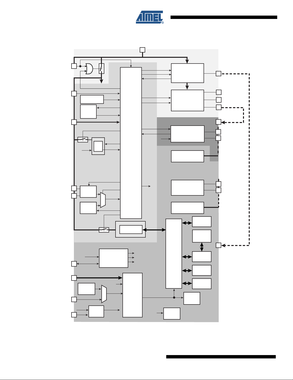
Figure 9-1. System Controller Block Diagram
VDDIO1
FWUP
NRSTB
WKUP0 - WKUP15
XIN
XOUT
Zero-Power
Power-on Reset
Brownout
SLCK
Xtal 32 kHz
Embedded
32 kHz RC
Detector
Oscillator
Oscillator
brown_out
RTC
osc32k_xtal_en
osc32k_sel
osc32k_rc_en
Backup Power Supply
supply_on
bod_on
rtc_on
rtc_nreset
rtc_alarm
Slow Clock
SLCK
sram_on
Supply
Controller
SRAM 2 Kbytes
vr_on
vr_mode
vr_ok
lcd_mode
lcd_out
lcd_nreset
lcd_eof
core_nreset
Software Controlled
Voltage Regulator
LCD Power Supply
Segment
SLCK
Controller
PIOA - PIOB
LCD
Charge
Pump
LCD
ADC
PIOC
VDDOUT
CAPM1-CAPP1
CAPM2-CAPP2
VDDLCD
VDDLCD
SEG0 - SEG39
COM0 - COM7
ADVREF
AD0 - AD3
SRAM
4 kbytes
Peripherals
30
proc_nreset
periph_nreset
ice_nreset
Power
Management
Controller
Master Clock
MCK
SLCK
NRST
FSTT0 - FSTT15
FCIN
PLLRC
core_nreset
Embedded
2 MHz RC
Oscillator
SLCK PLLCK
PLL
Reset
Controller
SLCK
Main Clock
MAINCK
AT91SAM7L128/64 Preliminary
Memory
Controller
Watchdog
Timer
VDDCORE
Peripheral
Bridge
ARM7TDMI
Flash
Periodic
Interval
Timer
Core Power Supply
6257AS–ATARM–28-Feb-08

9.2 Supply Controller (SUPC)
The Supply Controller controls the power supplies of each section of the product:
• the processor and the peripherals
• the Flash memory
• the backup SRAM
• the LCD controller, the charge pump and the LCD voltage regulator
• the Real Time Clock
The Supply Controller has its own reset circuitry and is clocked by the 32 kHz Slow clock
generator.
The reset circuitry is based on the NRSTB pin, a zero-power power-on reset cell and a brownout
detector cell. The zero-power power-on reset allows the Supply Controller to start properly, while
the software-programmable brownout detector allows detection of either a battery discharge or
main voltage loss.
The Slow Clock generator is based on a 32 kHz crystal oscillator and an embedded 32 kHz RC
oscillator. The Slow Clock defaults to the RC oscillator, but the software can enable the crystal
oscillator and select it as the Slow Clock source.
The Supply Controller starts up the device by sequentially enabling the internal power switches
and the Voltage Regulator, then it generates the proper reset signals to the core power supply.
AT91SAM7L128/64 Preliminary
It also enables to set the system in different low power modes and to wake it up from a wide
range of events.
9.3 Reset Controller
• Based on one power-on reset cell and a brownout detector
• Status of the last reset; either power-up reset, software reset, user reset, watchdog reset,
brownout reset
• Controls the internal resets and the NRST pin output
• Allows to shape a signal on the NRST line, guaranteeing that the length of the pulse meets
any requirement.
9.3.1 Brownout Detector (BOD) and Power-on Reset
The AT91SAM7L128/64 embeds one zero-power power-on reset and a brownout detection circuit. Both monitor VDDIO1.
The zero-power power-on reset circuit is always active. It provides an internal reset signal to the
AT91SAM7L128/64 for power-on and power-off operations and ensures a proper reset for the
Supply Controller.
The brownout detection circuit is disabled by default and can be enabled by software. It monitors
VDDIO1.
The brownout detection circuit is factory calibrated.
6257AS–ATARM–28-Feb-08
The threshold is programmable via software. It can be selected from 1.9V to 3.4V with 100 mV
steps. It can be programmed to generate either a wake-up alarm or a reset.
It can be used to wake up the chip from backup mode if the supply drops below a selected
threshold (to warn the end user about a discharged battery for example) and to reset the chip
when the voltage is too low.
31

BOD current consumption is 25 µA, typically.
To decrease current consumption, the software can disable the brownout detector, especially in
low-power mode.
The software can also configure the BOD in “switched” mode. In this mode, an internal state
machine switches on and off periodically and stores the output of the BOD.
This decreases the current consumption (inferior to 2 µA) while the detection is still active. This
feature is suitable in low-power mode where voltage detection is still needed.
9.4 Clock Generator
The clock generator embeds one low-power RC oscillator, one fast RC oscillator, one crystal
oscillator and one PLL with the following characteristics:
It provides SLCK, MAINCK and PLLCK.
The Supply Controller selects between the internal RC oscillator and the 32 kHz crystal oscillator. The unused oscillator is disabled so that power consumption is optimized.
The 2 MHz Fast RC oscillator is the default selected clock (MAINCK) which is used at start-up .
The user can select an external clock (CLKIN) through software.
• RC Oscillator ranges between 22 kHz and 42 kHz
• Fast RC Oscillator ranges between 1.5 MHz and 2.5 MHz
• Crystal Oscillator at 32 kHz (can be bypassed)
• PLL output ranges between 18 MHz and 47 MHz
The PLL needs an external RC filter and starts up in a very short time (inferior to 1 ms).
32
AT91SAM7L128/64 Preliminary
6257AS–ATARM–28-Feb-08
AT91SAM7L128/64 Preliminary
Figure 9-2. Clock Generator Block Diagram
Clock Generator
CLKIN
Embedded
2 MHz RC
Oscillator
OSCSEL
Embedded
32 kHz RC
Oscillator
XIN
XOUT
Xtal 32 kHz
Oscillator
Slow Clock
SLCK
MCK_SEL
Main Clock
MAINCK
9.5 Power Management Controller
The Power Management Controller uses the clock generator outputs to provide:
• The Processor Clock PCK
• The Master Clock MCK
• All the peripheral clocks, independently controllable
• Three programmable clock outputs PCKx
The Master Clock (MCK) is programmable from a few hundred Hz to the maximum operating frequency of the device.
The Processor Clock (PCK) switches off when entering processor idle mode, thus allowing
reduced power consumption while waiting for an interrupt.
The LCD Controller clock is SCLK.
PLLRC
SLCK
Power
Management
Controller
PLL and
Divider
ControlStatus
PLL Clock
PLLCK
6257AS–ATARM–28-Feb-08
33

Figure 9-3. Power Management Controller Block Diagram
9.6 Advanced Interrupt Controller
• Controls the interrupt lines (nIRQ and nFIQ) of an ARM Processor
• Individually maskable and vectored interrupt sources
– Source 0 is reserved for the Fast Interrupt Input (FIQ)
– Source 1 is reserved for system peripherals (RTC, PIT, EFC, PMC, DBGU, etc.)
– Other sources control the peripheral interrupts or external interrupts
– Programmable edge-triggered or level-sensitive internal sources
– Programmable positive/negative edge-triggered or high/low level-sensitive external
sources
• 8-level Priority Controller
– Drives the normal interrupt nIRQ of the processor
– Handles priority of the interrupt sources
– Higher priority interrupts can be served during service of lower priority interrupt
• Vectoring
– Optimizes interrupt service routine branch and execution
– One 32-bit vector register per interrupt source
– Interrupt vector register reads the corresponding current interrupt vector
•Protect Mode
– Easy debugging by preventing automatic operations
•Fast Forcing
– Permits redirecting any interrupt source on the fast interrupt
• General Interrupt Mask
– Provides processor synchronization on events without triggering an interrupt
SLCK
MAINCK
PLLCK
SLCK
MAINCK
PLLCK
Master Clock Controller
Prescaler
/1,/2,/4,...,/64
Programmable Clock Controller
Prescaler
/1,/2,/4,...,/64
Processor
Clock
Controller
Idle Mode
Peripherals
Clock Controller
ON/OFF
PCK
int
MCK
periph_clk[2..14]
pck[0..2]
9.7 Debug Unit
34
AT91SAM7L128/64 Preliminary
• Comprises:
– One two-pin UART
– One Interface for the Debug Communication Channel (DCC) support
6257AS–ATARM–28-Feb-08

– One set of Chip ID Registers
– One Interface providing ICE Access Prevention
•Two-pin UART
– USART-compatible User Interface
– Programmable Baud Rate Generator
– Parity, Framing and Overrun Error
– Automatic Echo, Local Loopback and Remote Loopback Channel Modes
• Debug Communication Channel Support
– Offers visibility of COMMRX and COMMTX signals from the ARM Processor
• Chip ID Registers
– Identification of the device revision, sizes of the embedded memories, set of
– Chip ID is 0x2733 0740 (VERSION 0) for AT91SAM7L128
– Chip ID is 0x2733 0540 (VERSION 0) for AT91SAM7L64
9.8 Period Interval Timer
• 20-bit programmable counter plus 12-bit interval counter
AT91SAM7L128/64 Preliminary
peripherals
9.9 Watchdog Timer
9.10 Real-time Clock
9.11 PIO Controllers
• 12-bit key-protected Programmable Counter running on prescaled SLCK
• Provides reset or interrupt signals to the system
• Counter may be stopped while the processor is in debug state or in idle mode
• Two Hundred Year Calendar
• Programmable Periodic Interrupt
• Time, Date and Alarm 32-bit Parallel Load
• Three PIO Controllers.
– PIO A controls 26 I/O lines
– PIO B controls 24 I/O lines
– PIO C controls 30 I/O lines
• Fully programmable through set/clear registers
• Multiplexing of two peripheral functions per I/O line
• For each I/O line (whether assigned to a peripheral or used as general-purpose I/O)
– Input change interrupt
– Half a clock period glitch filter
– Multi-drive option enables driving in open drain
– Programmable pull-up on each I/O line
– Pin data status register, supplies visibility of the level on the pin at any time
• Synchronous output, provides Set and Clear of several I/O lines in a single write
6257AS–ATARM–28-Feb-08
35

10. Peripherals
10.1 User Interface
The User Peripherals are mapped in the 256 MBytes of the address space between
0xF000 0000 and 0xFFFF EFFF. Each peripheral is allocated 16 Kbytes of address space.
A complete memory map is presented in Figure 8-1 on page 24.
10.2 Peripheral Identifiers
The AT91SAM7L128/64 embeds a wide range of peripherals. Table 10-1 defines the Peripheral
Identifiers of the AT91SAM7L128/64. Unique peripheral identifiers are defined for both the
Advanced Interrupt Controller and the Power Management Controller.
Table 10-1. Peripheral Identifiers
Peripheral
ID
0 AIC Advanced Interrupt Controller FIQ
1 SYSIRQ
2 PIOA Parallel I/O Controller A
3 PIOB Parallel I/O Controller B
4 PIOC Parallel I/O Controller C
5 SPI Serial Peripheral Interface
6 US0 USART 0
7 US1 USART 1
8 Reserved
9 TWI Two-wire Interface
10 PWMC PWM Controller
11 SLCDC Segmented LCD Controller
12 TC0 Timer/Counter 0
13 TC1 Timer/Counter 1
14 TC2 Timer/Counter 2
15 ADC
16 - 29 Reserved
30 AIC Advanced Interrupt Controller IRQ0
31 AIC Advanced Interrupt Controller IRQ1
Peripheral
Mnemonic
(1)
(1)
Peripheral
Name
System Interrupt
Analog-to Digital Converter
External
Interrupt
36
Note: 1. Setting SYSIRQ and ADC bits in the clock set/clear registers of the PMC has no effect. The
System Controller and ADC are continuously clocked. The ADC clock is automatically started
for the first conversion. In Sleep Mode the ADC clock is automatically stopped after each
conversion.
AT91SAM7L128/64 Preliminary
6257AS–ATARM–28-Feb-08

10.3 Peripheral Multiplexing on PIO Lines
The AT91SAM7L128/64 features three PIO controllers, PIOA, PIOB and PIOC, that multiplex
the I/O lines of the peripheral set.
PIO Controller A, B and C control respectively 26, 24 and 30 lines. Each line can be assigned to
one of two peripheral functions, A or B.
Table 10-2 on page 38 defines how the I/O lines of the peripherals A, B or the analog inputs are
multiplexed on the PIO Controller A, B and C. The two columns “Function” and “Comments”
have been inserted for the user’s own comments; they may be used to track how pins are
defined in an application.
Note that some peripheral functions that are output only may be duplicated in the table.
At reset, all I/O lines are automatically configured as input with the programmable pull-up
enabled, so that the device is maintained in a static state as soon as a reset is detected.
AT91SAM7L128/64 Preliminary
6257AS–ATARM–28-Feb-08
37

10.4 PIO Controller A Multiplexing
Table 10-2. Multiplexing on PIO Controller A
PIO Controller A Application Usage
I/O Line Peripheral A Peripheral B Extra Function Function Comments
PA 0 C OM 0
PA 1 C OM 1
PA 2 C OM 2
PA 3 C OM 3
PA 4 C OM 4
PA 5 C OM 5
PA6 SEG0
PA7 SEG1
PA8 SEG2
PA9 SEG3
PA10 SEG4
PA11 SEG5
PA12 SEG6
PA13 SEG7
PA14 SEG8
PA15 SEG9
PA16 SEG10
PA17 SEG11
PA18 SEG12
PA 19
PA 20
PA21 SEG15
PA 22 SEG16
PA23 SEG17
PA 24 SEG18
PA25 SEG19
SEG13
SEG14
38
AT91SAM7L128/64 Preliminary
6257AS–ATARM–28-Feb-08

AT91SAM7L128/64 Preliminary
10.5 PIO Controller B Multiplexing
Table 10-3. Multiplexing on PIO Controller B
PIO Controller B Application Usage
I/O Line Peripheral A Peripheral B Extra Function Function Comments
PB0 SEG20
PB1 SEG21
PB2 SEG22
PB3 SEG23
PB4 SEG24
PB5 SEG25
PB6 SEG26
PB7 SEG27
PB8 SEG28
PB9 SEG29
PB10 SEG30
PB11 SEG31
PB12 NPCS3 SEG32
PB13 NPCS2 SEG33
PB14 NPCS1 SEG34
PB15 RTS1 SEG35
PB16 RTS0 SEG36
PB17 DTR1 SEG37
PB18 PWM0 SEG38
PB19 PWM1 SEG39
PB20 PWM2 COM6
PB21 PWM3 COM7
PB22 NPCS1 PCK1 COM8
PB23 PCK0 NPCS3 COM9
6257AS–ATARM–28-Feb-08
39

10.6 PIO Controller C Multiplexing
Table 10-4. Multiplexing on PIO Controller C
PIO Controller C Application Usage
I/O Line Peripheral A Peripheral B Extra Functions Function Comments
PC0 CTS1 PWM2 PGMEN0/WKUP0
PC1 DCD1 TIOA2 PGMEN1/WKUP1
PC2 DTR1 TIOB2 PGMEN2/WKUP2
PC3 DSR1 TCLK1 PGMNCMD/WKUP3
PC4 RI1 TCLK2 PGMRDY/WKUP4
PC5 IRQ1 NPCS2 PGMNOE/WKUP5
PC6 NPCS1 PCK2
PGMNVALID/WKUP6
2)
PC7 PWM0 TIOA0 PGMMO/High drive
PC8 PWM1 TIOB0 PGMM1/High drive
PC9 PWM2 SCK0 PGMM2/High drive
PC10 TWD NPCS3 PGMM3/High drive
PC11 TWCK TCLK0 PGMD0/WKUP7
PC12 RXD0 NPCS3 PGMD1/WKUP8
PC13 TXD0 PCK0 PGMD2/WKUP9
PC14 RTS0 ADTRG PGMD3/WKUP10
PC15 CTS0 PWM3 PGMD4/WKUP11
PC16 DRXD NPCS1 PGMD5
(1)(2)
(1)(2)
(1)(2)
(1)(2)
(1)(2)
(1)(2)
(1)(
(1)(2)
(1)(2)
(1)(2)
(1)(2)
(1)(2)
PC17 DTXD NPCS2 PGMD6
PC18 NPCS0 PWM0 PGMD7
PC19 MISO PWM1 PGMD8
PC20 MOSI PWM2 PGMD9
PC21 SPCK PWM3 PGMD10
PC22 NPCS3 TIOA1 PGMD11
PC23 PCK0 TIOB1 PGMD12
PC24 RXD1 PCK1 PGMD13
PC25 TXD1 PCK2 PGMD14
PC26
RTS0 FIQ PGMD15/WKUP12
PC27 NPCS2 IRQ0 WKUP13
PC28 SCK1 PWM0 WKUP14
PC29 RTS1 PWM1 WKUP15
Notes: 1. Wake-Up source in Backup mode (managed by the SUPC).
2. Fast Start-Up source in Wait mode (managed by the PMC).
(1)(2)
(1)(2)
(1)(2)
(1)(2)
40
AT91SAM7L128/64 Preliminary
6257AS–ATARM–28-Feb-08

10.7 Serial Peripheral Interface
• Supports communication with external serial devices
– Four chip selects with external decoder allow communication with up to 15
peripherals
– Serial memories, such as DataFlash
– Serial peripherals, such as ADCs, DACs, LCD Controllers, CAN Controllers and
Sensors
– External co-processors
• Master or slave serial peripheral bus interface
– 8- to 16-bit programmable data length per chip select
– Programmable phase and polarity per chip select
– Programmable transfer delays per chip select, between consecutive transfers and
between clock and data
– Programmable delay between consecutive transfers
– Selectable mode fault detection
– Maximum frequency at up to Master Clock
AT91SAM7L128/64 Preliminary
®
and 3-wire EEPROMs
10.8 Two Wire Interface
• Master, Multi-Master and Slave Mode Operation
• Compatibility with Atmel two-wire interface, serial memory and I
• One, two or three bytes for slave address
• Sequential read/write operations
• Bit Rate: Up to 400 kbit/s
• General Call Supported in Slave Mode
• Connecting to PDC channel capabilities optimizes data transfers in Master Mode only
10.9 USART
• Programmable Baud Rate Generator
• 5- to 9-bit full-duplex synchronous or asynchronous serial communications
2
– One channel for the receiver, one channel for the transmitter
– Next buffer support
– 1, 1.5 or 2 stop bits in Asynchronous Mode
– 1 or 2 stop bits in Synchronous Mode
– Parity generation and error detection
– Framing error detection, overrun error detection
– MSB or LSB first
– Optional break generation and detection
– By 8 or by 16 over-sampling receiver frequency
– Hardware handshaking RTS - CTS
– Modem Signals Management DTR-DSR-DCD-RI on USART1
– Receiver time-out and transmitter timeguard
C compatible devices
6257AS–ATARM–28-Feb-08
41
10.10 Timer Counter
– Multi-drop Mode with address generation and detection
– Optional Manchester Encoding
• RS485 with driver control signal
• ISO7816, T = 0 or T = 1 Protocols for interfacing with smart cards
– NACK handling, error counter with repetition and iteration limit
• IrDA modulation and demodulation
– Communication at up to 115.2 Kbps
• Test Modes
– Remote Loopback, Local Loopback, Automatic Echo
• Three 16-bit Timer Counter Channels
– Three output compare or two input capture
• Wide range of functions including:
– Frequency measurement
– Event counting
– Interval measurement
– Pulse generation
– Delay timing
– Pulse Width Modulation
– Up/down capabilities
• Each channel is user-configurable and contains:
– Three external clock inputs
• Five internal clock inputs, as defined in Table 10-5
Table 10-5. Timer Counter Clock Assignment
10.11 PWM Controller
42
AT91SAM7L128/64 Preliminary
TC Clock input Clock
TIMER_CLOCK1 MCK/2
TIMER_CLOCK2 MCK/8
TIMER_CLOCK3 MCK/32
TIMER_CLOCK4 MCK/128
TIMER_CLOCK5 MCK/1024
– Two multi-purpose input/output signals
– Two global registers that act on all three TC channels
• Four channels, one 16-bit counter per channel
• Common clock generator, providing thirteen different clocks
– One Modulo n counter providing eleven clocks
– Two independent linear dividers working on modulo n counter outputs
6257AS–ATARM–28-Feb-08

• Independent channel programming
– Independent enable/disable commands
– Independent clock selection
– Independent period and duty cycle, with double buffering
– Programmable selection of the output waveform polarity
– Programmable center or left aligned output waveform
10.12 Analog-to-Digital Converter
• 4-channel ADC supplied by the internal voltage regulator
• 10-bit 460 Ksamples/sec. or 8-bit 660 Ksamples/sec. Successive Approximation Register
ADC
• ±2 LSB Integral Non Linearity, ±1 LSB Differential Non Linearity
• Integrated 4-to-1 multiplexer
• External voltage reference for better accuracy on low voltage inputs
• Individual enable and disable of each channel
• Multiple trigger sources
– Hardware or software trigger
– External trigger pin
– Timer Counter 0 to 2 outputs TIOA0 to TIOA2 trigger
• Sleep Mode and conversion sequencer
– Automatic wakeup on trigger and back to sleep mode after conversions of all
enabled channels
AT91SAM7L128/64 Preliminary
10.13 Segment LCD Controller
The Segment LCD Controller/driver is intended for monochrome passive liquid crystal display
(LCD) with up to 10 common terminals and up to 40 segment terminals.
• 40 segments and 10 common terminals display capacity
• Support static, 1/2, 1/3, 1/4, 1/5, 1/6, 1/7, 1/8, 1/9 and 1/10 Duty
• Support static, 1/2, 1/3, 1/4 Bias
• Power-save mode display
• Software-selectable low-power waveform capability
• Flexible frame frequency selection
• Segment and common pins, not needed for driving the display, can be used as ordinary I/O
pins
• Switching time enhancement internal buffers
6257AS–ATARM–28-Feb-08
43

11. Package Drawings
Figure 11-1. 128-lead LQFP Package Drawing
44
.
Table 11-1. Device and LQFP Package Maximum Weight
AT91SAM7L128/64 800 mg
Table 11-2. Package Reference
JEDEC Drawing Reference MS-026
JESD97 Classification e3
Table 11-3. LQFP Package Characteristics
Moisture Sensitivity Level 3
AT91SAM7L128/64 Preliminary
6257AS–ATARM–28-Feb-08

Figure 11-2. 144-lead LFBGA Package Drawing
AT91SAM7L128/64 Preliminary
All dimensions are in mm
Table 11-4. Device and LFBGA Package Maximum Weight
AT91SAM7L128/64 mg
Table 11-5. Package Reference
JEDEC Drawing Reference MS-026
JESD97 Classification e1
Table 11-6. LFBGA Package Characteristics
Moisture Sensitivity Level 3
This package respects the recommendations of the NEMI User Group.
6257AS–ATARM–28-Feb-08
45

12. Ordering Information
Table 12-1. Ordering Information
Ordering Code Package Package Type Temperature Operating Range
AT91SAM7L128-AU LQFP128 Green Industrial (-40°C to 85°C)
AT91SAM7L64-AU LQFP128 Green Industrial (-40°C to 85°C)
AT91SAM7L128-CU LFBGA144 Green Industrial (-40°C to 85°C)
AT91SAM7L64-CU LFBGA144 Green Industrial (-40°C to 85°C)
46
AT91SAM7L128/64 Preliminary
6257AS–ATARM–28-Feb-08

Revision History
Doc. Rev Comments
6257AS First issue
AT91SAM7L128/64 Preliminary
Change
Request
Ref.
6257AS–ATARM–28-Feb-08
47
 Loading...