

Page 1

BDTIC www.bdtic.com/ATMEL
Features
• Incorporates the ARM7TDMI
– High-performance 32-bit RISC Architecture
– High-density 16-bit Instruction Set
– Leader in MIPS/Watt
– Little-endian
– EmbeddedICE
• 8-, 16- and 32-bit Read and Write Support
• 256K Bytes of On-chip SRAM
– 32-bit Data Bus
– Single-clock Cycle Access
• Fully Programmable External Bus Interface (EBI)
– Maximum External Address Space of 64M Bytes
– Up to Eight Chip Selects
– Software Programmable 8/16-bit External Data Bus
• Eight-level Priority, Individually Maskable, Vectored Interrupt Controller
– Four External Interrupts, including a High-priority, Low-latency Interrupt Request
• 32 Programmable I/O Lines
• Three-channel 16-bit Timer/Counter
– Three External Clock Inputs
– Two Multi-purpose I/O Pins per Channel
• Two USARTs
– Two Dedicated Peripheral Data Controller (PDC) Channels per USART
• Programmable Watchdog Timer
• Advanced Power-saving Features
– CPU and Peripheral Can be Deactivated Individually
• Fully Static Operation:
– 0 Hz to 75 MHz Internal Frequency Range at VDDCORE = 1.8V, 85°C
• 2.7V to 3.6V I/O Operating Range
• 1.65V to 1.95V Core Operating Range
• -40°C to +85° C Temperature Range
• Available in 100-lead LQFP Package (Green)
™
(In-circuit Emulation)
®
ARM® Thumb® Processor Core
AT91 ARM
Thumb-based
Microcontroller
AT91R40008
Summary
1. Description
The AT91R40008 microcontroller is a member of the Atmel AT91 16/32-bit microcontroller family, which is based on the ARM7TDMI processor core. This processor has a
high-performance, 32-bit RISC architecture with a high-density, 16-bit instruction set
and very low power consumption. Furthermore, it features 256K bytes of on-chip
SRAM and a large number of internally banked registers, resulting in very fast exception handling, and making the device ideal for real-time control applications.
The AT91R40008 microcontroller features a direct connection to off-chip memory,
including Flash, through the fully programmable External Bus Interface (EBI). An 8level priority vectored interrupt controller, in conjunction with the Peripheral Data Controller, significantly improves the real-time performance of the device.
The device is manufactured using Atmel’s high-density CMOS technology. By combining the ARM7TDMI processor core with a large, on-chip, high-speed SRAM and a
wide range of peripheral functions on a monolithic chip, the AT91R40008 is a powerful
microcontroller that offers a flexible and high-performance solution to many computeintensive embedded control applications.
Note: This is a summary document. A complete document
is available on our Web site at www.atmel.com.
http://www.atmel.com/dyn/resources/prod_documents/doc
1354.pdf
1732FS–ATARM–12-Apr-06
Page 2
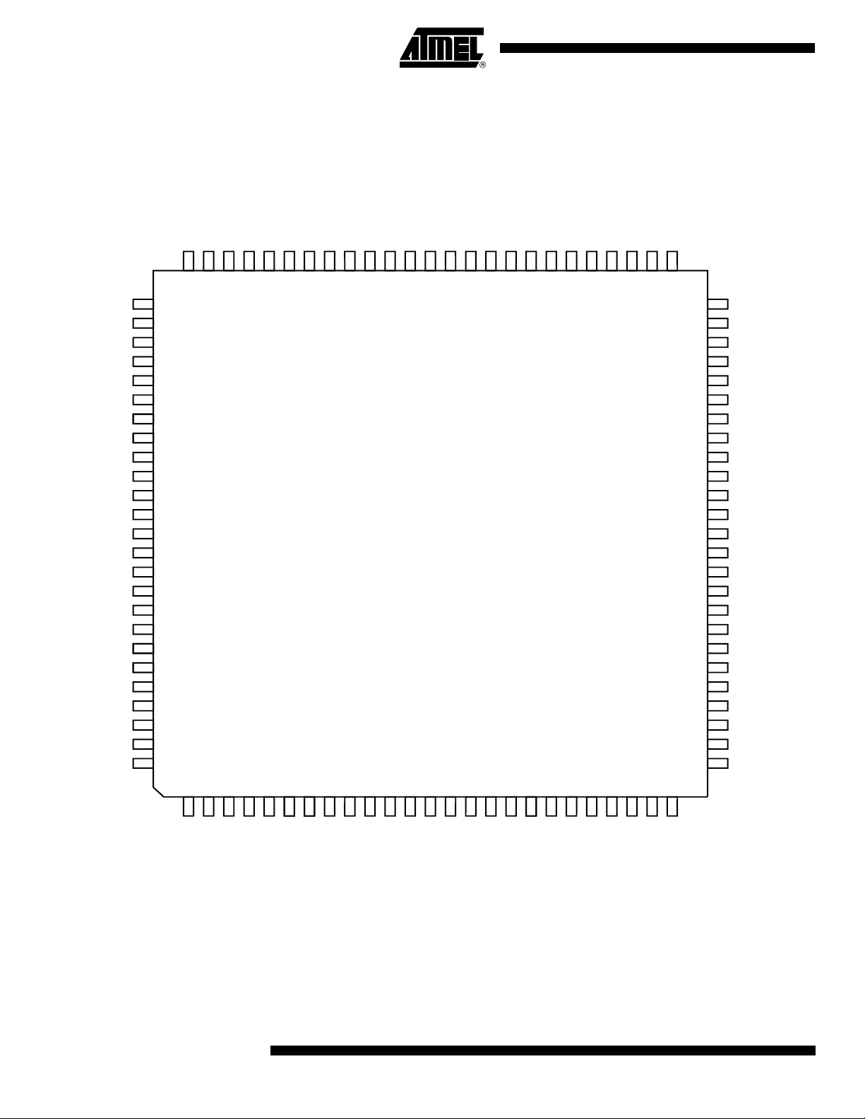
2. Pin Configuration
Figure 2-1. AT91R40008 in 100-lead LQFP Package
P16
P15/RXD0
P14/TXD0
P13/SCK0
P21/TXD1/NTRI
P18
P20/SCK1
P19
P17
P12/FIQ
GND
P10/IRQ1
P11/IRQ2
VDDIO
VDDCORE
P9/IRQ0
P8/TIOB2
P7/TIOA2
P6/TCLK2
P4/TIOA1
P5/TIOB1
P3/TCLK1
GND
GND
P2/TIOB0
P22/RXD1
NWR1/NUB
GND
NRST
NWDOVF
VDDIO
MCKI
P23
P24/BMS
P25/MCKO
GND
GND
TMS
TDI
TDO
TCK
NRD/NOE
NWR0/NWE
VDDCORE
VDDIO
NWAIT
NCS0
NCS1
P26/NCS2
P27/NCS3
7551747372717069686766656463626160595857565554
76
77
78
79
80
81
82
83
84
85
86
87
88
89
90
91
92
93
94
95
96
97
98
99
100
53
52
50
49
48
47
46
45
44
43
42
41
40
39
38
37
36
35
34
33
32
31
30
29
28
27
26
P1/TIOA0
P0/TCLK0
D15
D14
D13
D12
VDDIO
D11
D10
D9
D8
D7
D6
D5
GND
D4
D3
D2
D1
D0
P31/A23/CS4
P30/A22/CS5
VDDIO
VDDCORE
P29/A21/CS6
1252
3
4
5
6
7
8
9
GND
A0/NLB
A1
A2A2
A3
A5A6A7
A4
101112131415116171819202122
A9
A8
VDDIO
A10
A11
A12
A13
A14
GND
GND
A15
A16
A17
23
A18
24
A19
P28/A20/CS7
2
AT91R40008
1732FS–ATARM–12-Apr-06
Page 3

3. Pin Description
Table 3-1. AT91R40008 Pin Description
Module Name Function Type
A0 - A23 Address Bus Output – All valid after reset
D0 - D15 Data Bus I/O –
NCS0 - NCS3 Chip Select Output Low
CS4 - CS7 Chip Select Output High A23 - A20 after reset
NWR0 Lower Byte 0 Write Signal Output Low Used in Byte Write option
NWR1 Upper Byte 1 Write Signal Output Low Used in Byte Write option
EBI
AIC
TC
NRD Read Signal Output Low Used in Byte Write option
NWE Write Enable Output Low Used in Byte Select option
NOE Output Enable Output Low Used in Byte Select option
NUB Upper Byte Select Output Low Used in Byte Select option
NLB Lower Byte Select Output Low Used in Byte Select option
NWAIT Wait Input Input Low
BMS Boot Mode Select Input – Sampled during reset
FIQ Fast Interrupt Request Input – PIO-controlled after reset
IRQ0 - IRQ2 External Interrupt Request Input – PIO-controlled after reset
TCLK0 - TCLK2 Timer External Clock Input – PIO-controlled after reset
TIOA0 - TIOA2 Multipurpose Timer I/O pin A I/O – PIO-controlled after reset
AT91R40008
Active
Level Comments
TIOB0 - TIOB2 Multipurpose Timer I/O pin B I/O – PIO-controlled after reset
SCK0 - SCK1 External Serial Clock I/O – PIO-controlled after reset
USART
PIO P0 - P31 Parallel IO line I/O –
WD NWDOVF Watchdog Overflow Output Low Open-drain
Clock
Reset
ICE
Power
TXD0 - TXD1 Transmit Data Output Output – PIO-controlled after reset
RXD0 - RXD1 Receive Data Input Input – PIO-controlled after reset
MCKI Master Clock Input Input – Schmidt trigger
MCKO Master Clock Output Output –
NRST Hardware Reset Input Input Low Schmidt trigger
NTRI Tri-state Mode Select Input Low Sampled during reset
TMS Test Mode Select Input – Schmidt trigger, internal pull-up
TDI Test Data Input Input – Schmidt trigger, internal pull-up
TDO Test Data Output Output –
TCK Test Clock Input – Schmidt trigger, internal pull-up
VDDIO I/O Power Power – 3V nominal supply
VDDCORE Core Power Power – 1.8V nominal supply
GND Ground Ground –
1732FS–ATARM–12-Apr-06
3
Page 4
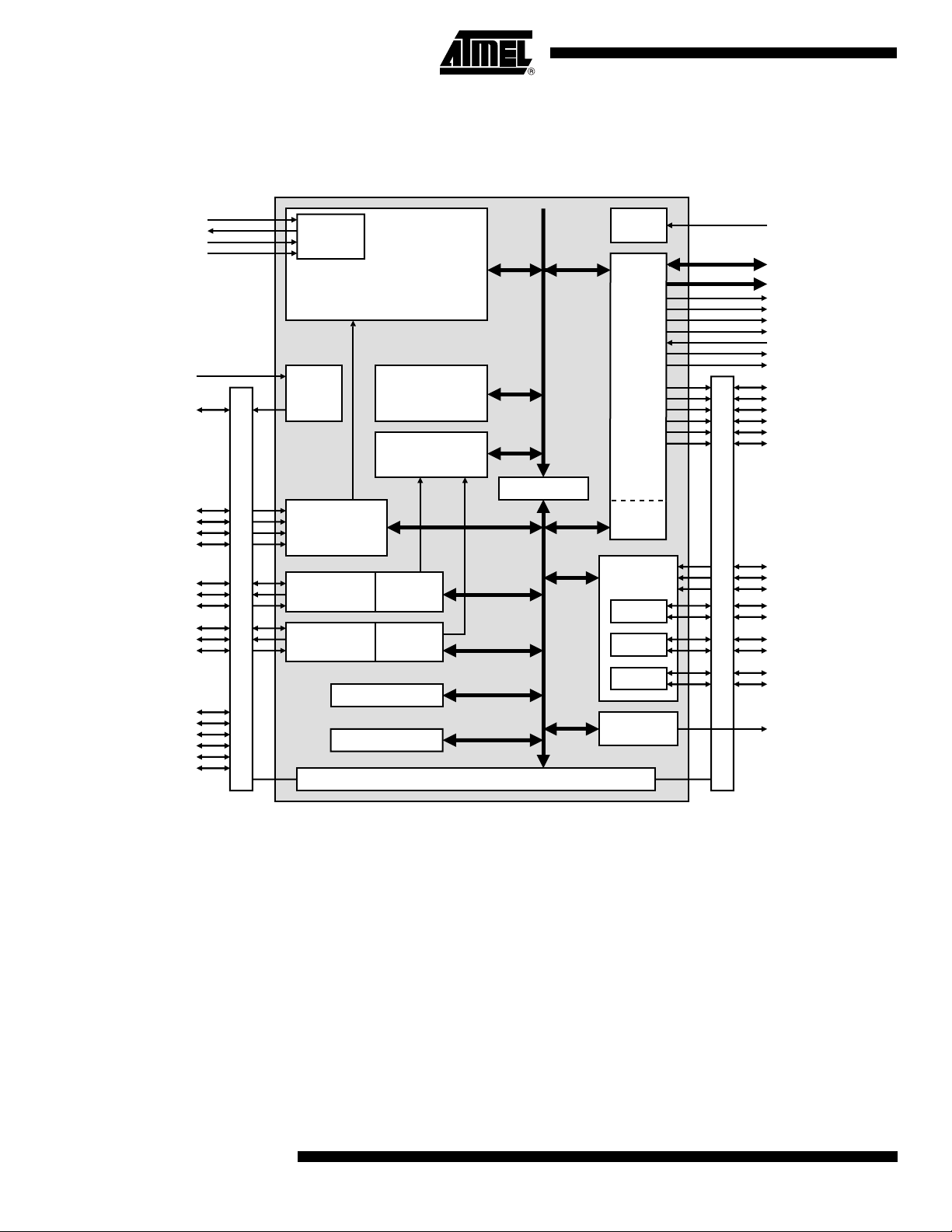
4. Block Diagram
Figure 4-1. AT91R40008
MCKI
P25/MCKO
P12/FIQ
P9/IRQ0
P10/IRQ1
P11/IRQ2
P13/SCK0
P14/TXD0
P15/RXD0
P20/SCK1
P21/TXD1/NTRI
P22/RXD1
P16
P17
P18
P19
P23
P24/BMS
TMS
TDO
TDI
TCK
Embedded
ICE
Reset
ARM7TDMI Core
ASB
Clock
AIC: Advanced
Interrupt Controller
P
I
O
USART0
USART1
256K Bytes RAM
ASB
Controller
2 PDC
Channels
2 PDC
Channels
PS: Power Saving
Chip ID
PIO: Parallel I/O Controller
AMBA Bridge
APB
EBI: External Bus Interface
EBI User
Interface
TC: Timer
Counter
TC0
TC1
TC2
WD: Watchdog
Timer
P
I
O
NRST
D0-D15
A1-A19
A0/NLB
NRD/NOE
NWR0/NWE
NWR1/NUB
NWAIT
NCS0
NCS1
P26/NCS2
P27/NCS3
P28/A20/CS7
P29/A21/CS6
P30/A22/CS5
P31/A23/CS4
P0/TCLK0
P3/TCLK1
P6/TCLK2
P1/TIOA0
P2/TIOB0
P4/TIOA1
P5/TIOB1
P7/TIOA2
P8/TIOB2
NWDOVF
4
AT91R40008
1732FS–ATARM–12-Apr-06
Page 5

5. Architectural Overview
The AT91R40008 microcontroller integrates an ARM7TDMI with EmbeddedICE interface,
memories and peripherals. The architecture consists of two main buses: the Advanced System Bus (ASB) and the Advanced Peripheral Bus (APB). Designed for maximum performance
and controlled by the memory controller, the ASB interfaces the ARM7TDMI processor with
the on-chip 32-bit memories, the External Bus Interface (EBI) and the AMBA
AMBA Bridge drives the APB, which is designed for accesses to on-chip peripherals and optimized for low power consumption.
The AT91R40008 microcontroller implements the ICE port of the ARM7TDMI processor on
dedicated pins, offering a complete, low-cost and easy-to-use debug solution for target
debugging.
5.1 Memories
The AT91R40008 microcontroller embeds 256K bytes of internal SRAM. The internal memory
is directly connected to the 32-bit data bus and is single-cycle accessible.
The AT91R40008 microcontroller features an External Bus Interface (EBI), which enables
connection of external memories and application-specific peripherals. The EBI supports 8- or
16-bit devices and can use two 8-bit devices to emulate a single 16-bit device. The EBI implements the early read protocol, enabling faster memory accesses than standard memory
interfaces.
AT91R40008
™
Bridge. The
5.2 Peripherals
The AT91R40008 microcontrollers integrate several peripherals, that are classified as system
or user peripherals. All on-chip peripherals are 32-bit accessible by the AMBA Bridge, and can
be programmed with a minimum number of instructions. The peripheral register set consists of
control, mode, data, status and enable/disable/status registers.
An on-chip Peripheral Data Controller (PDC) transfers data between the on-chip USARTs and
on- and off-chip memories address space without processor intervention. Most importantly,
the PDC removes the processor interrupt handling overhead, making it possible to transfer up
to 64K contiguous bytes without reprogramming the start address, thus increasing the performance of the microcontroller and reducing the power consumption.
5.2.1 System Peripherals
The External Bus Interface (EBI) controls the external memory or peripheral devices via an 8or 16-bit data bus and is programmed through the Advanced Peripheral Bus (APB). Each chip
select line has its own programming register.
The Power-saving (PS) module implements the Idle mode (ARM7TDMI core clock stopped
until the next interrupt) and enables the user to adapt the power consumption of the microcontroller to application requirements (independent peripheral clock control).
The Advanced Interrupt Controller (AIC) controls the internal interrupt sources from the internal peripherals and the four external interrupt lines (including the FIQ) to provide an interrupt
and/or fast interrupt request to the ARM7TDMI. It integrates an 8-level priority controller and,
using the Auto-vectoring feature, reduces the interrupt latency time.
1732FS–ATARM–12-Apr-06
The Parallel Input/Output Controller (PIO) controls up to 32 I/O lines. It enables the user to
select specific pins for on-chip peripheral input/output functions and general-purpose
5
Page 6

5.2.2 User Peripherals
input/output signal pins. The PIO controller can be programmed to detect an interrupt on a signal change from each line.
The Watchdog (WD) can be used to prevent system lock-up if the software becomes trapped
in a deadlock.
The Special Function (SF) module integrates the Chip ID, the Reset Status and the Protect
registers.
Two independently configurable USARTs enable communication at a high baud rate in synchronous or asynchronous mode. The format includes start, stop and parity bits and up to 8
data bits. Each USART also features a Time-out and a Time-guard register, facilitating the
use of the two dedicated Peripheral Data Controller (PDC) channels.
The 3-channel, 16-bit Timer/Counter (TC) is highly programmable and supports capture or
waveform modes. Each TC channel can be programmed to measure or generate different
kinds of waves, and can detect and control two input/output signals. The TC also has three
external clock signals.
6
AT91R40008
1732FS–ATARM–12-Apr-06
Page 7

AT91R40008
6. Associated Documentation
The AT91R40008 is part of the AT91X40 series of microcontrollers, a member of the Atmel AT91 16/32-bit microcontroller
family, which is based on the ARM7TDMI processor core. The table below contains details of associated documentation for
further reference.
Associated Documentation
Product Information Document Title
Internal architecture of processor
ARM/Thumb instruction sets
Embedded in-circuit-emulator
External memory interface mapping
Peripheral operations
Peripheral user interfaces
ARM7TDMI (Thumb) Datasheet
AT91x40 Series Datasheet
AT91R40008
DC characteristics
Power consumption
Thermal and reliability considerations
AC characteristics
Product overview
Ordering information
Packaging information
Soldering profile
AT91R40008 Electrical Characteristics
AT91R40008 Summary Datasheet (this document)
1732FS–ATARM–12-Apr-06
7
Page 8

7. Product Overview
7.1 Power Supply
The AT91R40008 microcontroller has two types of power supply pins:
• VDDCORE pins, which power the chip core (i.e., the ARM7TDMI, embedded memory and
the peripherals).
• VDDIO pins, which power the I/O lines.
An independent I/O supply allows a flexible adaptation to external component signal levels.
7.2 Input/Output Considerations
After the reset, the peripheral I/Os are initialized as inputs to provide the user with maximum
flexibility. It is recommended that in any application phase, the inputs to the AT91R40008
microcontroller be held at valid logic levels to minimize the power consumption.
7.3 Master Clock
The AT91R40008 microcontroller has a fully static design and works on the Master Clock
(MCK) provided on the MCKI pin from an external source.
The Master Clock is also provided as an output of the device on the pin MCKO, which is multiplexed through a general-purpose I/O line. While NRST is active, MCKO remains low. After
the reset, the MCKO is valid and outputs an image of the MCK signal. The PIO controller must
be programmed to use this pin as standard I/O line.
7.4 Reset
Reset restores the default states of the user interface registers (defined in the user interface of
each peripheral) and forces the ARM7TDMI to perform the next instruction fetch from address
zero. Except for the program counter, the ARM7TDMI registers do not have defined reset
states.
7.4.1 NRST Pin
NRST is active low-level input. It is asserted asynchronously, but exit from reset is synchronized internally to the MCK. The signal presented on MCKI must be active within the
specification for a minimum of 10 clock cycles up to the rising edge of NRST to ensure correct
operation.
The first processor fetch occurs 80 clock cycles after the rising edge of NRST.
7.4.2 Watchdog Reset
The Watchdog can be programmed to generate an internal reset. In this case, the reset has
the same effect as the NRST pin assertion, but the pins BMS and NTRI are not sampled. Boot
Mode and Tri-state Mode are not updated. If the NRST pin is asserted and the Watchdog trig
gers the internal reset, the NRST pin has priority.
7.5 Emulation Functions
7.5.1 Tri-state Mode
The AT91R40008 microcontroller provides a tri-state mode, which is used for debug purposes.
This enables the connection of an emulator probe to an application board without having to
desolder the device from the target board. In tri-state mode, all the output pin drivers of the
AT91R40008 microcontroller are disabled.
-
8
AT91R40008
1732FS–ATARM–12-Apr-06
Page 9

To enter tri-state mode, the NTRI pin must be held low during the last 10 clock cycles before
the rising edge of NRST. For normal operation, the NTRI pin must be held high during reset by
a resistor of up to 400 kΩ.
NTRI is multiplexed with I/O line P21 and USART1 serial data transmit line TXD1.
Standard RS-232 drivers generally contain internal 400 kΩ pull-up resistors. If TXD1 is con-
nected to a device not including this pull-up, the user must make sure that a high level is tied
on NTRI while NRST is asserted.
7.5.2 JTAG/ICE Debug
ARM standard embedded in-circuit emulation is supported via the JTAG/ICE port. The pins
TDI, TDO, TCK and TMS are dedicated to this debug function and can be connected to a host
computer via the external ICE interface.
In ICE Debug mode, the ARM7TDMI core responds with a non-JTAG chip ID that identifies the
microcontroller. This is not fully IEEE1149.1 compliant.
7.6 Memory Controller
The ARM7TDMI processor address space is 4G bytes. The memory controller decodes the
internal 32-bit address bus and defines three address spaces:
• Internal memories in the four lowest megabytes
• Middle space reserved for the external devices (memory or peripherals) controlled by the
• Internal peripherals in the four highest megabytes
In any of these address spaces, the ARM7TDMI operates in Little-endian mode only.
AT91R40008
EBI
7.6.1 Internal Memories
7.6.2 Boot Mode Select
The AT91R40008 microcontroller integrates 256K bytes of internal SRAM. All internal memories are 32 bits wide and single-clock cycle accessible. Byte (8-bit), half-word (16-bit) or word
(32-bit) accesses are supported and are executed within one cycle. Fetching Thumb or ARM
instructions is supported and internal memory can store twice as many Thumb instructions as
ARM ones.
The SRAM is mapped at address 0x0 (after the Remap command), allowing ARM7TDMI
exception vectors between 0x0 and 0x20 to be modified by the software.
Placing the SRAM on-chip and using the 32-bit data bus bandwidth maximizes the microcontroller performance and minimizes the system power consumption. The 32-bit bus increases
the effectiveness of the use of the ARM instruction set and the ability of processing data that is
wider than 16-bit, thus making optimal use of the ARM7TDMI advanced performance.
Being able to dynamically update application software in the 256-Kbyte SRAM adds an extra
dimension to the AT91R40008.
The ARM reset vector is at address 0x0. After the NRST line is released, the ARM7TDMI executes the instruction stored at this address. This means that this address must be mapped in
nonvolatile memory after the reset.
The input level on the BMS pin during the last 10 clock cycles before the rising edge of the
NRST selects the type of boot memory (see Table 7-1).
1732FS–ATARM–12-Apr-06
9
Page 10

7.6.3 Remap Command
7.6.4 Abort Control
The BMS pin is multiplexed with the I/O line P24, which can be programmed after reset like
any standard PIO line.
Table 7-1. Boot Mode Select
BMS Boot Memory
1 External 8-bit memory on NCS0
0 External 16-bit memory on NCS0
The ARM vectors (Reset, Abort, Data Abort, Pre-fetch Abort, Undefined Instruction, Interrupt,
Fast Interrupt) are mapped from address 0x0 to address 0x20. In order to allow these vectors
to be redefined dynamically by the software, the AT91R40008 microcontroller uses a Remap
command that enables switching between the boot memory and the internal primary SRAM
bank addresses. The Remap command is accessible through the EBI User Interface by writing
one in RCB of EBI_RCR (Remap Control Register). Performing a Remap command is mandatory if access to the other external devices (connected to chip-selects 1 to 7) is required. The
Remap operation can only be changed back by an internal reset or an NRST assertion.
The abort signal providing a Data Abort or a Pre-fetch Abort exception to the ARM7TDMI is
asserted when accessing an undefined address in the EBI address space.
No abort is generated when reading the internal memory or by accessing the internal peripherals, whether or not the address is defined.
7.6.5 External Bus Interface
The External Bus Interface handles the accesses between addresses 0x0040 0000 and
0xFFC0 0000. It generates the signals that control access to the external devices, and can be
configured from eight 1M byte banks up to four 16M bytes banks. It supports byte-, half-wordand word-aligned accesses.
For each of these banks, the user can program:
• Number of wait states
• Number of data float times (wait time after the access is finished to prevent any bus
contention in case the device is too long in releasing the bus)
• Data bus width (8-bit or 16-bit)
The user can program the EBI to control one 16-bit device (Byte Select Access mode) with a
16-bit wide data bus or two 8-bit devices in parallel that emulate a 16-bit memory (Byte Write
Access mode).
The External Bus Interface also features the Early Read Protocol, configurable for all the
devices, which significantly reduces access time requirements on an external device in the
case of single-clock cycle access.
10
AT91R40008
1732FS–ATARM–12-Apr-06
Page 11

8. Peripherals
The AT91R40008 microcontroller peripherals are connected to the 32-bit wide Advanced
Peripheral Bus. Peripheral registers are only word accessible – byte and half-word accesses
are not supported. If a byte or a half-word access is attempted, the memory controller automatically masks the lowest address bits and generates a word access.
Each peripheral has a 16-Kbyte address space allocated (the AIC only has a 4-Kbyte address
space).
8.0.1 Peripheral Registers
The following registers are common to all peripherals:
• Control Register – write-only register that triggers a command when a one is written to the
• Mode Register – read/write register that defines the configuration of the peripheral. Usually
• Data Registers – read and/or write registers that enable the exchange of data between the
• Status Register – read-only register that returns the status of the peripheral.
• Enable/Disable/Status Registers are shadow command registers. Writing a one in the
Unused bits in the peripheral registers are shown as “–” and must be written at 0 for upward
compatibility. These bits read 0.
AT91R40008
corresponding position at the appropriate address. Writing a zero has no effect.
has a value of 0x0 after a reset.
processor and the peripheral.
Enable Register sets the corresponding bit in the Status Register. Writing a one in the
Disable Register resets the corresponding bit and the result can be read in the Status
Register. Writing a bit to zero has no effect. This register access method maximizes the
efficiency of bit manipulation and enables modification of a register with a single noninterruptible instruction, replacing the costly read-modify-write operation.
8.0.2 Peripheral Interrupt Control
The Interrupt Control of each peripheral is controlled from the Status Register using the interrupt mask. The Status Register bits are ANDed to their corresponding interrupt mask bits and
the result is then ORed to generate the Interrupt Source signal to the Advanced Interrupt
Controller.
The interrupt mask is read in the Interrupt Mask Register and is modified with the Interrupt
Enable Register and the Interrupt Disable Register. The enable/disable/status (or mask)
makes it possible to enable or disable peripheral interrupt sources with a non-interruptible single instruction. This eliminates the need for interrupt masking at the AIC or Core level in realtime and multi-tasking systems.
8.0.3 Peripheral Data Controller
The AT91R40008 microcontroller has a 4-channel PDC dedicated to the two on-chip USARTs.
One PDC channel is dedicated to the receiver and one to the transmitter of each USART.
The user interface of a PDC channel is integrated in the memory space of each USART. It
contains a 32-bit Address Pointer Register (RPR or TPR) in addition to a 16-bit Transfer
Counter Register (RCR or TCR). When the programmed number of transfers are performed, a
status bit indicating the end of transfer is set in the USART Status Register and an interrupt
can be generated.
1732FS–ATARM–12-Apr-06
11
Page 12

8.1 System Peripherals
8.1.1 PS: Power-saving
The Power-saving feature optimizes power consumption, enabling the software to stop the
ARM7TDMI clock (Idle mode), restarting it when the module receives an interrupt (or reset). It
also enables on-chip peripheral clocks to be enabled and disabled individually, matching
power consumption and application need.
8.1.2 AIC: Advanced Interrupt Controller
The Advanced Interrupt Controller has an 8-level priority, individually maskable, vectored
interrupt controller, and drives the NIRQ and NFIQ pins of the ARM7TDMI from:
• The external fast interrupt line (FIQ)
• The three external interrupt request lines (IRQ0 - IRQ2)
• The interrupt signals from the on-chip peripherals
The AIC is extensively programmable offering maximum flexibility, and its vectoring features
reduce the real-time overhead in handling interrupts.
The AIC also features a spurious vector, which reduces spurious interrupt handling to a minimum, and a protect mode that facilitates the debug capabilities.
8.1.3 PIO: Parallel I/O Controller
The AT91R40008 microcontroller has 32 programmable I/O lines. Six pins are dedicated as
general-purpose I/O pins. Other I/O lines are multiplexed with an external signal of a peripheral to optimize the use of available package pins. The PIO controller enables generation of an
interrupt on input change on any of the PIO pins.
8.1.4 WD: Watchdog
The Watchdog is built around a 16-bit counter and is used to prevent system lock-up if the software becomes trapped in a deadlock. It can generate an internal reset or interrupt, or assert
an active level on the dedicated pin NWDOVF. All programming registers are password-protected to prevent unintentional programming.
8.1.5 SF: Special Function
The AT91R40008 microcontroller provides registers that implement the following special
functions:
• Chip identification
• RESET status
• Protect mode
12
AT91R40008
1732FS–ATARM–12-Apr-06
Page 13

8.2 User Peripherals
8.2.1 USART: Universal Synchronous/
Asynchronous Receiver Transmitter
The AT91R40008 microcontroller provides two identical, full-duplex, universal synchronous/asynchronous receiver/transmitters.
Each USART has its own baud rate generator and two dedicated Peripheral Data Controller
channels. The data format includes a start bit, up to 8 data bits, an optional programmable parity bit and up to 2 stop bits.
The USART also features a Receiver Time-out Register, facilitating variable length frame support when it is working with the PDC, and a Time-guard Register, used when interfacing with
slow remote equipment.
8.2.2 TC: Timer/Counter
The AT91R40008 microcontroller features a Timer/Counter block that includes three identical
16-bit Timer/Counter channels. It is possible to independently program each channel to perform a wide range of functions, including frequency measurement, event counting, interval
measurement, pulse generation, delay timing and pulse width modulation.
The Timer/Counter can be used in Capture or Waveform mode, and all three counter channels
can be started simultaneously and chained together.
AT91R40008
1732FS–ATARM–12-Apr-06
13
Page 14
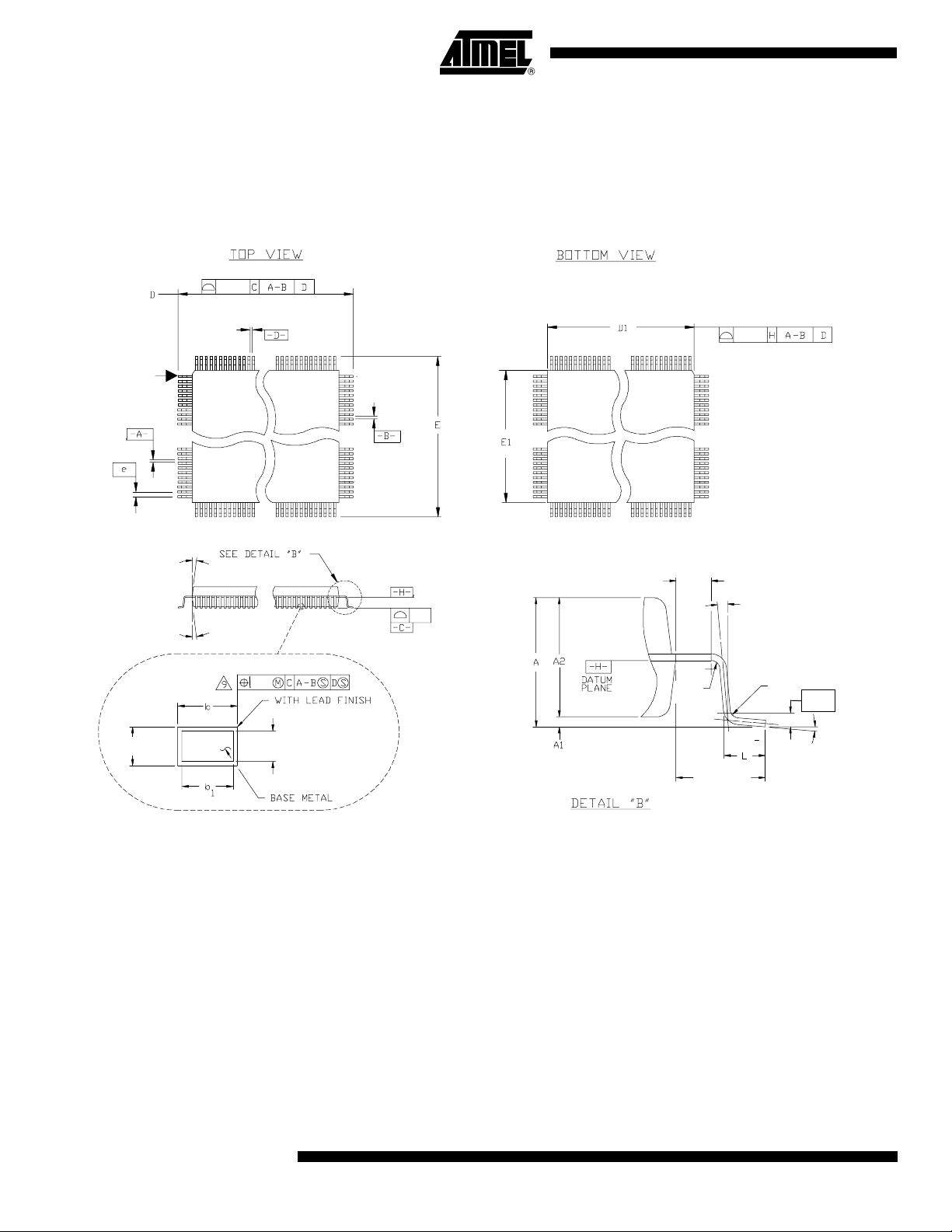
9. Packaging Information
Figure 9-1. 100-lead Thin Quad Flat Pack Package Outline
aaa
PIN 1
bbb
ddd
cc
1
ccc
S
R1
1
L1
R2
0.25
14
AT91R40008
1732FS–ATARM–12-Apr-06
Page 15

Table 9-1. Common Dimensions (mm)
Symbol Min Nom Max
c 0.09 0.2
c1 0.09 0.16
L 0.45 0.6 0.75
L1 1.00 REF
R2 0.08 0.2
R1 0.08
S0.2
q0° 3.5° 7°
θ10°
θ2 11° 12° 13°
θ3 11° 12° 13°
A 1.6
A1 0.05 0.15
A2 1.35 1.4 1.45
AT91R40008
Tolerances of Form and Position
aaa 0.2
bbb 0.2
Table 9-2. Lead Count Dimensions (mm)
Pin
Count
100 16.0 14.0 0.17 0.22 0.27 0.17 0.2 0.23 0.50 0.10 0.06
D/E
BSC
D1/E1
BSC
bb1
e
BSC ccc dddMin Nom Max Min Nom Max
Table 9-3. Device and 100-lead LQFP Package Maximum Weight
710 mg
Table 9-4. 100-lead LQFP Package Characteristics
Moisture Sensitivity Level 3
1732FS–ATARM–12-Apr-06
15
Page 16

10. Soldering Profile
10.1 LQFP Package Soldering Profile (Green)
Table 10-1 gives the recommended soldering profile from J-STD-020C.
Table 10-1. Soldering Profile Green Compliant Package
Profile Feature Green Package
Average Ramp-up Rate (217°C to Peak) 3°C/sec. max.
Preheat Temperature 175°C ±25°C 180 sec. max.
Temperature Maintained Above 217°C 60 sec. to 150 sec.
Time within 5°C of Actual Peak Temperature 20 sec. to 40 sec.
Peak Temperature Range 260 +0 °C
Ramp-down Rate 6°C/sec. max.
Time 25°C to Peak Temperature 8 min. max.
Note: The package is certified to be backward compatible with Pb/Sn soldering profile.
A maximum of three reflow passes is allowed per component.
16
AT91R40008
1732FS–ATARM–12-Apr-06
Page 17

11. Ordering Information
Table 11-1. Ordering Information
Ordering Code Package Package Type Operation Range
AT91R40008-66AU LQFP 100 Green
AT91R40008
Industrial
(-40°C to 85° C)
1732FS–ATARM–12-Apr-06
17
Page 18

Revision History
Doc. Rev Date Comments
1732AS Jun-01 First issue
1732BS Jul-01 Updated
1732CS 29-Jan-02
pg. 9 Added information to Internal Memories
pg. 14 Changed Table 4
pg. 16 Added Table 6, Package Weight
pg. 17 Added section, Soldering Profile
1732DS 17-Mar-04
pg. 1 Features: Fully Static Operation; frequency changed
pg. 16 Added Table 8, 100-Lead LQFP Package Characteristics
1732ES 14-Jun-05
Change
Request
Ref.
1732FS 12-Apr-06
Global
pg. 17 added 10.1 ”LQFP Package Soldering Profile (Green)”
pg. 18 new package info inserted in 11. ”Ordering Information”
page 16
page 17
New corporate format numbering
package reference TQFP changed to LQFP
10. ”Soldering Profile” and
11. ”Ordering Information”
AT91R40006-66AI LQFP 100, Sn/Pb package ref. removed.
CSR 05-328
#2601
18
AT91R40008
1732FS–ATARM–12-Apr-06
 Loading...