

Page 1

Features
• Utilizes the ARM7TDMI
– High-performance 32-bit RISC Architecture
– High-density 16-bit Instruction Set
– Leader in MIPS/Watt
– Embedded ICE (In-Circuit Emulation)
• 8K Bytes Internal SRAM
• Fully-programmable External Bus Interface (EBI)
– Maximum External Address Space of 128M Bytes
– Eight Chip Selects
– Software Programmable 8/16-bit External Databus
• 8-level Priority, Individually Maskable, Vectored Interrupt Controller
– Seven External Interrupts, Including a High-priority, Low-latency Interrupt Request
• Fifty-eight Programmable I/O Lines
• 6-channel 16-bit Timer/Counter
– Six External Clock Inputs and Two Multi-purpose I/O Pins per Channel
• Three USARTs
• Master/Slave SPI Interface
– 8-bit to 16-bit Programmable Data Length
– Four External Slave Chip Selects
• Programmable Watchdog Timer
• 8-channel 10-bit ADC
• 2-channel 10-bit DAC
• Clock Generator with On-chip Main Oscillator and PLL for Multiplication
– 3 to 20 MHz Frequency Range Main Oscillator
• Real-time Clock with On-chip 32 kHz Oscillator
– Battery Backup Operation and External Alarm
• 8-channel Peripheral Data Controller for USARTs and SPIs
• Advanced Power Management Controller (APMC)
– Normal, Wait, Slow, Standby and Power-down modes
• IEEE 1149.1 JTAG Boundary-scan on all Digital Pins
• Fully Static Operation: 0 Hz to 33 MHz
• 2.7V to 3.6V Core Operating Range
• 2.7V to 5.5V I/O Operating Range
• 2.7V to 3.6V Analog Operating Range
• 1.8V to 3.6V Backup Battery Operating Range
• 2.7V to 3.6V Oscillator and PLL Operating Range
• -40°C to +85°C Temperature Range
• Available in a 176-lead LQFP or 176-ball BGA Package
®
ARM® Thumb® Processor Core
AT91
ARM
®
Thumb®
Microcontrollers
AT91M55800A
1. Description
The AT91M55800A is a member of the Atmel AT91 16/32-bit microcontroller family,
which is based on the ARM7TDMI processor core. This processor has a high-performance 32-bit RISC architecture with a high-density 16-bit instruction set and very low
power consumption. In addition, a large number of internally banked registers result in
very fast exception handling, making the device ideal for real-time control
applications.
The fully programmable External Bus Interface provides a direct connection to off-chip
memory in as fast as one clock cycle for a read or write operation. An eight-level prior-
Rev. 1745D–ATARM–04-Nov-05
Page 2

ity vectored interrupt controller in conjunction with the peripheral data controller significantly improve the real-time
performance of the device.
The device is manufactured using Atmel’s high-density CMOS technology. By combining the ARM7TDMI processor core
with an on-chip SRAM, a wide range of peripheral functions, analog interfaces and low-power oscillators on a monolithic
chip, the Atmel AT91M55800A is a powerful microcontroller that provides a highly-flexible and cost-effective solution to
many ultra low-power applications.
2
AT91M55800A
1745D–ATARM–04-Nov-05
Page 3

AT91M55800A
2. Pin Configurations
Table 2-1. Pin Configuration for 176-lead LQFP Package
Pin AT91M55800A Pin AT91M55800A Pin AT91M55800A Pin AT91M55800A
1 GND 45 GND 89 GND 133 GND
2 GND 46 GND 90 GND 134 GND
3 NCS0 47 D8 91 PA19/RXD1 135 NCS4
4 NCS1 48 D9 92 PA20/SCK2 136 NCS5
5 NCS2 49 D10 93 PA21/TXD2 137 NCS6
6 NCS3 50 D11 94 PA22/RXD2 138 NCS7
7 NLB/A0 51 D12 95 PA23/SPCK 139 PB0
8 A1 52 D13 96 PA24/MISO 140 PB1
9 A2 53 D14 97 PA25/MOSI 141 PB2
10 A3 54 D15 98 PA26/NPCS0/NSS 142 PB3/IRQ4
11 A4 55 PB19/TCLK0 99 PA27/NPCS1 143 PB4/IRQ5
12 A5 56 PB20/TIOA0 100 PA28/NPCS2 144 PB5
13 A6 57 PB21/TIOB0 101 PA29/NPCS3 145 PB6/AD0TRIG
14 A7 58 PB22/TCLK1 102 VDDIO 146 PB7/AD1TRIG
15 VDDIO 59 VDDIO 103 GND 147 VDDIO
16 GND 60 GND 104 VDDPLL 148 GND
17 A8 61 PB23/TIOA1 105 XIN 149 PB8
18 A9 62 PB24/TIOB1 106 XOUT 150 PB9
19 A10 63 PB25/TCLK2 107 GNDPLL 151 PB10
20 A11 64 PB26/TIOA2 108 PLLRC 152 PB11
21 A12 65 PB27/TIOB2 109 VDDBU
22 A13 66 PA0/TCLK3 110 XIN32
23 A14 67 PA1/TIOA3 111 XOUT32
24 A15 68 PA2/TIOB3 112 NRSTBU
25 A16 69 PA3/TCLK4 113 GNDBU
26 A17 70 PA4/TIOA4 114 WAKEUP
27 A18 71 PA5/TIOB4 115 SHDN
28 A19 72 PA6/TCLK5 116 GNDBU
29 VDDIO 73 VDDIO 117 VDDA
30 GND 74 GND 118 AD0
31 A20 75 PA7/TIOA5 119 AD1
32 A21 76 PA8/TIOB5 120 AD2
33 A22 77 PA9/IRQ0 121 AD3
34 A23 78 PA10/IRQ1 122 AD4
35 D0 79 PA11/IRQ2 123 AD5
36 D1 80 PA12/IRQ3 124 AD6
37 D2 81 PA13/FIQ 125 AD7
38 D3 82 PA14/SCK0 126 ADVREF
39 D4 83 PA15/TXD0 127 DAVREF
40 D5 84 PA16/RXD0 128 DA0
41 D6 85 PA17/SCK1 129 DA1
42 D7 86 PA18/TXD1/NTRI 130 GNDA
43 VDDCORE 87 VDDCORE 131 VDDCORE 175 VDDCORE
44 VDDIO 88 VDDIO 132 VDDIO 176 VDDIO
Notes: 1. Analog pins
2. Battery backup pins
(2)
(2)
(2)
(2)
(2)
(2)
(2)
(2)
(1)
(1)
(1)
(1)
(1)
(1)
(1)
(1)
(1)
(1)
(1)
(1)
(1)
(1)
153 PB12
154 PB13
155 PB14
156 PB15
157 PB16
158 PB17
159 NWDOVF
160 MCKO
161 VDDIO
162 GND
163 PB18/BMS
164 JTAGSEL
165 TMS
166 TDI
167 TDO
168 TCK
169 NTRST
170 NRST
171 NWAIT
172 NOE/NRD
173 NWE/NWR0
174 NUB/NWR1
1745D–ATARM–04-Nov-05
3
Page 4

Table 2-2. Pin Configuration for 176-ball BGA Package
Pin AT91M55800A Pin AT91M55800A Pin AT91M55800A Pin AT91M55800A
A1 NCS1 C1 A0/NLB E1 A4 G1 A12
A2 NWAIT C2 NCS0 E2 A3 G2 A9
A3 NRST C3 VDDIO E3 A5 G3 A8
A4 NTRST C4 VDDCORE E4 GND G4 GND
A5 PB18/BMS C5 TMS E5 – G5 –
A6 NWDOVF C6 VDDIO E6 – G6 –
A7 PB16 C7 MCK0 E7 – G7 –
A8 PB12 C8 PB13 E8 – G8 –
A9 PB10 C9 PB6/AD0TRIG E9 – G9 –
A10 PB9 C10 VDDIO E10 – G10 –
A11 PB8 C11 PB4/IRQ5 E11 – G11 –
A12 NCS7 C12 PB0 E12 AD6 G12 AD3
A13 NCS6 C13 VDDIO E13 AD5 G13 AD2
A14 GND C14 DA0 E14 NRSTBU G14 GND
A15 DAVREF C15 ADVREF E15 GNDBU G15 XIN32
B1 NCS2 D1 A2 F1 A10 H1 A15
B2 NUB/NWR1 D2 A1 F2 A7 H2 A14
B3 NWE/NWR0 D3 NCS3 F3 VDDIO H3 A13
B4 NOE/NRD D4 GND F4 A6 H4 A11
B5 TD0 D5 TCK F5 – H5 –
B6 TDI D6 JTAGSEL F6 – H6 –
B7 PB17 D7 GND F7 – H7 –
B8 PB11 D8 PB15 F8 – H8 –
B9 PB7/AD1TRIG D9 PB14 F9 – H9 –
B10 PB3/IRQ4 D10 PB5 F10 – H10 –
B11 PB2 D11 PB1 F11 – H11 –
B12 NCS5 D12 GND F12 GND H12 AD1
B13 NCS4 D13 VDDCORE F13 AD4 H13 AD0
B14 DA1 D14 AD7 F14 VDDBU H14 WAKEUP
B15 GNDA D15 VDDA F15 XOUT32 H15 GND
4
AT91M55800A
1745D–ATARM–04-Nov-05
Page 5

AT91M55800A
Table 2-2. Pin Configuration for 176-ball BGA Package (Continued)
Pin AT91M55800A Pin AT91M55800A Pin AT91M55800A Pin AT91M55800A
J1 A17 L1 A20 N1 D4 R1 D10
J2 A18 L2 A23 N2 D6 R2 D11
J3 VDDIO L3 D0 N3 VDDIO R3 D12
J4 A16 L4 D1 N4 D14 R4 D13
J5 – L5 – N5 PB19/TCLK0 R5 PB20/TIOA0
J6 – L6 – N6 VDDIO R6 PB23/TIOA1
J7 – L7 – N7 PB25/TCLK2 R7 PB24/TIOB1
J8 – L8 – N8 PA1/TIOA3 R8 PA3/TCLK4
J9 – L9 – N9 VDDIO R9 PA4/TIOA4
J10 – L10 – N10 PA8/TIOB5 R10 PA5/TIOB4
J11 – L11 – N11 PA9/IRQ0 R11 PA6/TCLK5
J12 PA29/NPCS3 L12 PA25/MOSI N12 VDDCORE R12 PA12/IRQ3
J13 SHDN L13 PA22RXD2 N13 VDDIO R13 PA14/SCK0
J14 VDDPLL L14 PA26/NPCS0/NSS N14 PA19/RXD1 R14 PA15/TXD0
J15 PLLRC L15 XOUT N15 GND R15 PA16/RXD0
K1 A19 M1 D2 P1 D5
K2 A22 M2 D3 P2 D7
K3 A21 M3 VDDCORE P3 D8
K4 GND M4 GND P4 D9
K5 – M5 GND P5 D15
K6 – M6 PB21/TIOB0 P6 PB22/TCLK1
K7 – M7 GND P7 PB26/TIOA2
K8 – M8 PB27/TIOB2 P8 PA2/TIOB3
K9 – M9 PA0/TCLK3 P9 PA7/TIOA5
K10 – M10 GND P10 PA10/IRQ1
K11 – M11 PA23/SPCK P11 PA11/IRQ2
K12 PA28/NPCS2 M12 GND P12 PA13/FIQ
K13 VDDIO M13 PA21/TXD2 P13 PA17SCK1
K14 PA27/NPCS1 M14 PA24/MISO P14 PA18/TXD1/NTRI
K15 GNDPLL M15 XIN P15 PA20/SCK2
1745D–ATARM–04-Nov-05
5
Page 6
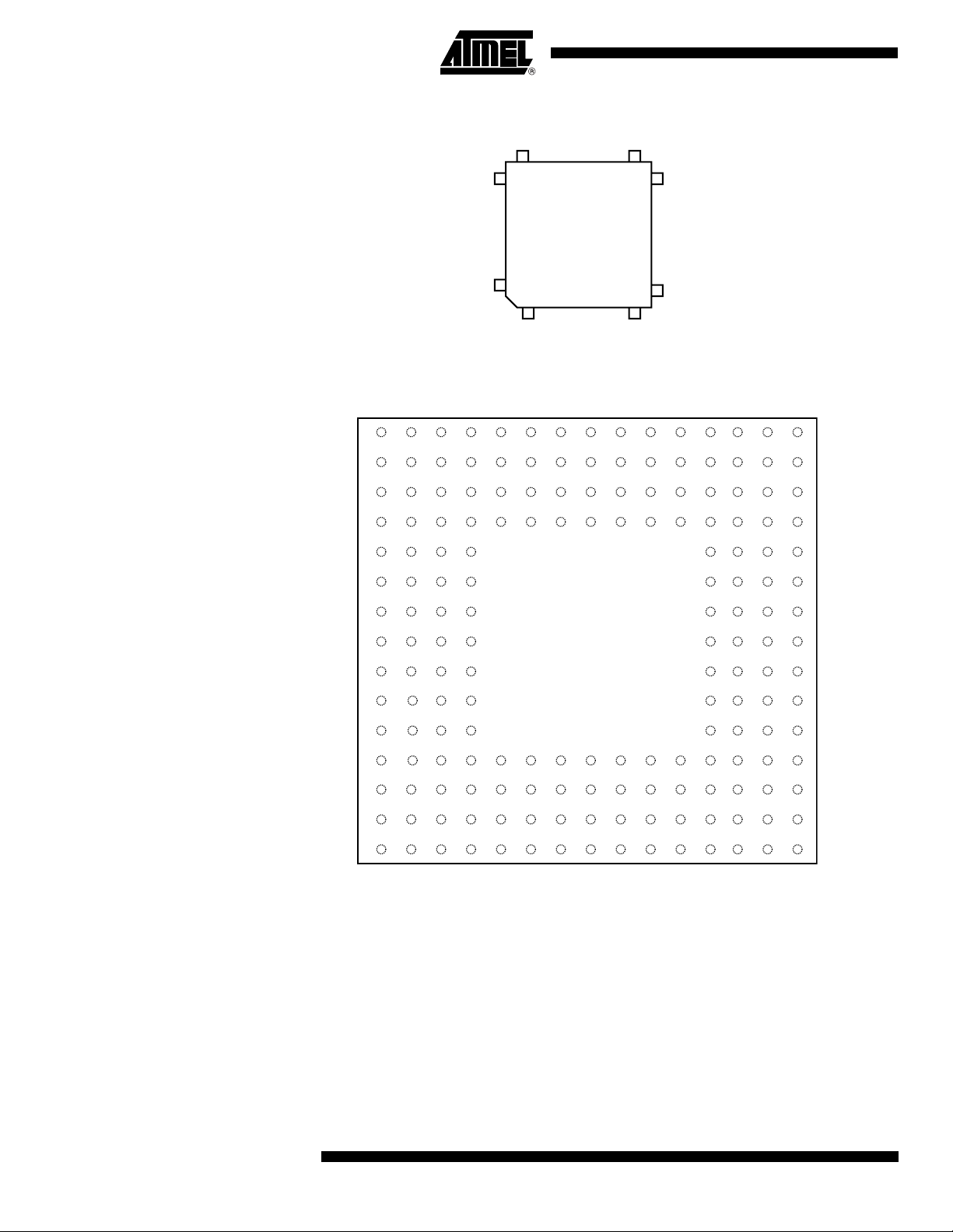
Figure 2-1. 176-lead LQFP Pinout
132 89
133
176
Figure 2-2. 176-ball BGA Pinout
123456789101112
A
B
C
D
E
F
G
88
45
144
13 14 15
H
J
K
L
M
N
P
R
6
AT91M55800A
1745D–ATARM–04-Nov-05
Page 7

3. Pin Description
Table 3-1. Pin Description
Module Name Function Type
A0 - A23 Address bus Output –
D0 - D15 Data bus I/O –
NCS0 - NCS7 Chip select Output Low
NWR0 Lower byte 0 write signal Output Low Used in Byte-write option
NWR1 Lower byte 1 write signal Output Low Used in Byte-write option
EBI
AIC
Timer
NRD Read signal Output Low Used in Byte-write option
NWE Write enable Output Low Used in Byte-select option
NOE Output enable Output Low Used in Byte-select option
NUB Upper byte-select Output Low Used in Byte-select option
NLB Lower byte-select Output Low Used in Byte-select option
NWAIT Wait input Input Low
BMS Boot mode select Input – Sampled during reset
IRQ0 - IRQ5 External interrupt request Input – PIO-controlled after reset
FIQ Fast external interrupt request Input – PIO-controlled after reset
TCLK0 - TCLK5 Timer external clock Input – PIO-controlled after reset
TIOA0 - TIOA5 Multipurpose timer I/O pin A I/O – PIO-controlled after reset
AT91M55800A
Active
Level Comments
TIOB0 - TIOB5 Multipurpose timer I/O pin B I/O – PIO-controlled after reset
SCK0 - SCK2 External serial clock I/O – PIO-controlled after reset
USART
SPI
PIO
WD NWDOVF Watchdog timer overflow Output Low Open drain
ADC
TXD0 - TXD2 Transmit data output Output – PIO-controlled after reset
RXD0 - RXD2 Receive data input Input – PIO-controlled after reset
SPCK SPI clock I/O – PIO-controlled after reset
MISO Master in slave out I/O – PIO-controlled after reset
MOSI Master out slave in I/O – PIO-controlled after reset
NSS Slave select Input Low PIO-controlled after reset
NPCS0 - NPCS3 Peripheral chip select Output Low PIO-controlled after reset
PA0 - PA29 Parallel I/O port A I/O – Input after reset
PB0 - PB27 Parallel I/O port B I/O – Input after reset
AD0-AD7 Analog input channels 0 - 7 Analog in –
AD0TRIG ADC0 external trigger Input – PIO-controlled after reset
AD1TRIG ADC1 external trigger Input – PIO-controlled after reset
ADVREF Analog reference Analog ref –
1745D–ATARM–04-Nov-05
7
Page 8

Table 3-1. Pin Description (Continued)
Module Name Function Type
DAC
Clock
APMC
Reset
JTAG/ICE
DA0 - DA1 Analog output channels 0 - 1 Analog out –
DAVREF Analog reference Analog ref –
XIN Main oscillator input Input –
XOUT Main oscillator output Output –
PLLRC RC filter for PLL Input –
XIN32 32 kHz oscillator input Input –
XOUT32 32 kHz oscillator output Output –
MCKO System clock Output –
WAKEUP Wakeup request Input –
SHDN Shutdown request Output – Tri-state after backup reset
NRST Hardware reset input Input Low Schmidt trigger
NRSTBU
NTRI Tri-state mode select Input Low Sampled during reset
JTAGSEL
TMS Test mode select Input – Schmidt trigger, internal pull-up
TDI Test data input Input – Schmidt trigger, internal pull-up
TDO Test data output Output –
TCK Test clock Input – Schmidt trigger, internal pull-up
NTRST Test reset input Input Low Schmidt trigger, internal pull-up
Hardware reset input for battery
part
Selects between ICE and JTAG
mode
Input Low Schmidt trigger
Input –
Active
Level Comments
Power
8
VDDA Analog power Analog pwr –
GNDA Analog ground Analog gnd –
VDDBU Power backup Power –
GNDBU Ground backup Ground –
VDDCORE Digital core power Power –
VDDIO Digital I/O power Power –
VDDPLL Main oscillator and PLL power Power –
GND Digital ground Ground –
GNDPLL PLL ground Ground –
AT91M55800A
1745D–ATARM–04-Nov-05
Page 9
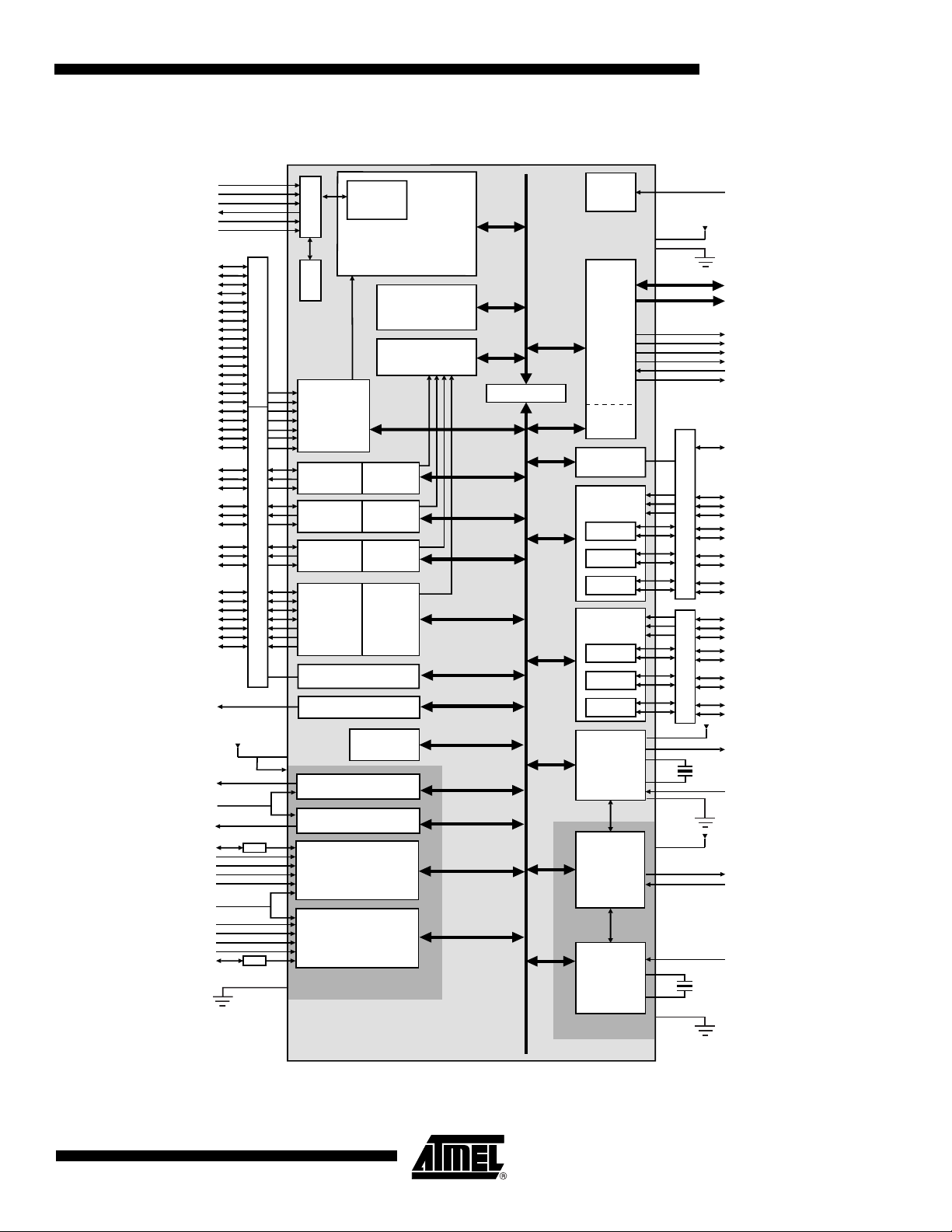
4. Block Diagram
AT91M55800A
JTAGSEL
NTRST
TMS
TDO
PB10
PB11
PB12
PB13
PB14
PB15
PB16
PB17
PB3/IRQ4
PB4/IRQ5
PA9/IRQ0
PA10/IRQ1
PA11/IRQ2
PA12/IRQ3
PA13/FIQ
PA14/SCK0
PA15/TXD0
PA16/RXD0
PA17/SCK1
PA18/TXD1/NTRI
PA19/RXD1
PA20/SCK2
PA21/TXD2
PA22/RXD2
PA23/SPCK
PA24/MISO
PA25/MOSI
PA26/NPCS0/NSS
PA27/NPCS1
PA28/NPCS2
PA29/NPCS3
NWDOVF
VDDA
DA0
DAVREF
DA1
PB6/AD0TRIG
AD0
AD1
AD2
AD3
ADVREF
AD4
AD5
AD6
AD7
PB7/AD1TRIG
GNDA
TDI
TCK
PB0
PB1
PB2
PB5
PB8
PB9
I
I
XIN
16 MHz
XOUT
XIN32
32.768 kHz
XOUT32
NRST
VDDIO, VDDCORE
GND
D0 - D15
A1 - A23
A0/NLB
NRD/NOE
NWR0/NWE
NWR1/NUB
NWAIT
NCS0 - NCS7
PB18/BMS
PB19/TCLK0
PB22/TCLK1
PB25/TCLK2
PB20/TIOA0
PB21/TIOB0
PB23/TIOA1
PB24/TIOB1
PB26/TIOA2
PB27/TIOB2
PA0/TCLK3
PA3/TCLK4
PA6/TCLK5
PA1/TIOA3
PA2/TIOB3
PA4/TIOA4
PA5/TIOB4
PA7/TIOA5
PA8/TIOB5
VDDPLL
MCKO
PLLRC
GNDPLL
VDDBU
SHDN
WAKEUP
NRSTBU
GNDBU
Embedded
ICE
Reset
JTAGSEL
ARM7TDMI Core
JTAG
2 PDC
Channels
2 PDC
Channels
2 PDC
Channels
2 PDC
Channels
Chip ID
Internal RAM
8K Bytes
ASB
Controller
P
I
O
B
AIC:
Advanced
Interrupt
Controller
USART0
P
I
O
A
USART1
USART2
SPI: Serial
Peripheral
Interface
PIOA Controller
WD: Watchdog Timer
DAC0
DAC1
4-Channel
ADC0
4-Channel
ADC1
Analog
ASB
AMBA Bridge
APB
EBI: External
Bus Interface
EBI User
Interface
PIOB
Controller
TC: Timer
Counter
Block 0
TC0
TC1
TC2
TC: Timer
Counter
Block 1
TC3
TC4
TC5
Clock
Generator
PLL
APMC:
Advanced
Power
Management
Controller
RTC:
Real Time
Clock
Battery Backup
P
O
B
P
O
A
1745D–ATARM–04-Nov-05
9
Page 10

5. Architectural Overview
The AT91M55800A microcontroller integrates an ARM7TDMI with its embedded ICE interface, memories and peripherals. Its architecture consists of two main buses, the Advanced
System Bus (ASB) and the Advanced Peripheral Bus (APB). Designed for maximum performance and controlled by the memory controller, the ASB interfaces the ARM7TDMI processor
with the on-chip 32-bit memories, the External Bus Interface (EBI) and the AMBA
The AMBA Bridge drives the APB, which is designed for accesses to on-chip peripherals and
optimized for low power consumption.
The AT91M55800A microcontroller implements the ICE port of the ARM7TDMI processor on
dedicated pins, offering a complete, low cost and easy-to-use debug solution for target
debugging.
5.1 Memory
The AT91M55800A microcontroller embeds 8K bytes of internal SRAM. The internal memory
is directly connected to the 32-bit data bus and is single-cycle accessible.
The AT91M55800A microcontroller features an External Bus Interface (EBI), which enables
connection of external memories and application-specific peripherals. The EBI supports 8- or
16-bit devices and can use two 8-bit devices to emulate a single 16-bit device. The EBI implements the early read protocol, enabling faster memory accesses than standard memory
interfaces.
™
Bridge.
5.2 Peripherals
The AT91M55800A microcontroller integrates several peripherals, which are classified as system or user peripherals. All on-chip peripherals are 32-bit accessible by the AMBA Bridge, and
can be programmed with a minimum number of instructions. The peripheral register set is
composed of control, mode, data, status and enable/disable/status registers.
An on-chip, 8-channel Peripheral Data Controller (PDC) transfers data between the on-chip
USARTs/SPI and the on and off-chip memories without processor intervention. One PDC
channel is connected to the receiving channel and one to the transmitting channel of each
USART and of the SPI.
Most importantly, the PDC removes the processor interrupt handling overhead and significantly reduces the number of clock cycles required for a data transfer. It can transfer up to 64K
contiguous bytes. As a result, the performance of the microcontroller is increased and the
power consumption reduced.
5.2.1 System Peripherals
The External Bus Interface (EBI) controls the external memory and peripheral devices via an
8- or 16-bit data bus and is programmed through the APB. Each chip select line has its own
programming register.
The Advanced Power Management Controller (APMC) optimizes power consumption of the
product by controlling the clocking elements such as the oscillators and the PLL, system and
user peripheral clocks, and the power supplies.
10
The Advanced Interrupt Controller (AIC) controls the internal interrupt sources from the internal peripherals and the eight external interrupt lines (including the FIQ), to provide an interrupt
and/or fast interrupt request to the ARM7TDMI. It integrates an 8-level priority controller and,
using the Auto-vectoring feature, reduces the interrupt latency time.
AT91M55800A
1745D–ATARM–04-Nov-05
Page 11

5.2.2 User Peripherals
AT91M55800A
The Real-time Clock (RTC) peripheral is designed for very low power consumption, and combines a complete time-of-day clock with alarm and a two-hundred year Gregorian calendar,
complemented by a programmable periodic interrupt.
The Parallel Input/Output Controllers (PIOA and PIOB) control the 58 I/O lines. They enable
the user to select specific pins for on-chip peripheral input/output functions, and general-purpose input/output signal pins. The PIO controllers can be programmed to detect an interrupt
on a signal change from each line.
The Watchdog (WD) can be used to prevent system lock-up if the software becomes trapped
in a deadlock.
The Special Function (SF) module integrates the Chip ID and Reset Status registers.
Three USARTs, independently configurable, enable communication at a high baud rate in synchronous or asynchronous mode. The format includes start, stop and parity bits and up to 8
data bits. Each USART also features a Timeout and a Time Guard Register, facilitating the
use of the two dedicated Peripheral Data Controller (PDC) channels.
The six 16-bit Timer/Counters (TC) are highly programmable and support capture or waveform
modes. Each TC channel can be programmed to measure or generate different kinds of
waves, and can detect and control two input/output signals. Each TC also has three external
clock signals.
The SPI provides communication with external devices in master or slave mode. It has four
external chip selects which can be connected to up to 15 devices. The data length is programmable, from 8- to 16-bits.
The two identical 4-channel 10-bit analog-to-digital converters (ADC) are based on a Successive Approximation Register (SAR) approach.
1745D–ATARM–04-Nov-05
11
Page 12

6. Associated Documentation
Table 6-1. Associated Documentation
Product Information Document Title
Internal architecture of processor
AT91M55800A
ARM/Thumb instruction sets
Embedded in-circuit-emulator
External memory interface mapping
Peripheral operations
Peripheral user interfaces
Ordering information
Packaging information
Soldering profile
Errata
DC Characteristics
Power consumption
Thermal and reliability coniderations
AC characteristics
Product overview
Ordering information
Packaging information
Soldering profile
ARM7TDMI (Thumb) Datasheet 0673
AT91M55800A Datasheet (This document) 1745
AT91M55800A Electrical Characteristics 1727
AT91M55800A Summary Datasheet 1745S
Literature
Number
12
AT91M55800A
1745D–ATARM–04-Nov-05
Page 13

7. Product Overview
7.1 Power Supplies
The AT91M55800A has 5 kinds of power supply pins:
• VDDCORE pins, which power the chip core
• VDDIO pins, which power the I/O Lines
• VDDPLL pins, which power the oscillator and PLL cells
• VDDA pins, which power the analog peripherals ADC and DAC
• VDDBU pins, which power the RTC, the 32768 Hz oscillator and the Shut-down Logic of
VDDIO and VDDCORE are separated to permit the I/O lines to be powered with 5V, thus
resulting in full TTL compliance.
The following ground pins are provided:
• GND for both VDDCORE and VDDIO
• GNDPLL for VDDPLL
•GNDA for VDDA
• GNDBU for VDDBU
All of these ground pins must be connected to the same voltage (generally the board electric
ground) with wires as short as possible. GNDPLL, GNDA and GNDBU are provided separately in order to allow the user to add a decoupling capacitor directly between the power and
ground pads. In the same way, the PLL filter resistor and capacitors must be connected to the
device and to GNDBU with wires as short as possible. Also, the main oscillator crystal and the
32768 Hz crystal external load capacitances must be connected respectively to GNDPLL and
to GNDBU with wires as short as possible.
AT91M55800A
the APMC
The main constraints applying to the different voltages of the device are:
• VDDBU must be lower than or equal to VDDCORE
• VDDA must be higher than or equal to VDDCORE
• VDDCORE must be lower than or equal to VDDIO
The nominal power combinations supported by the AT91M55800A are described in the following table:
Table 7-1. Nominal Power Combinations
VDDIO VDDCORE VDDA VDDPLL VDDBU
3V 3V 3V 3V 3V 33 MHz
3.3V 3.3V 3.3V 3.3V 3.3V 33 MHz
5V 3.3V 3.3V 3.3V 3.3V 33 MHz
7.2 Input/Output Considerations
After the reset, the peripheral I/Os are initialized as inputs to provide the user with maximum
flexibility. It is recommended that in any application phase, the inputs to the AT91M55800A
microcontroller be held at valid logic levels to minimize the power consumption.
Maximum Operating
Frequency
1745D–ATARM–04-Nov-05
13
Page 14

7.3 Master Clock
7.4 Reset
7.4.1 NRST Pin
Master Clock is generated in one of the following ways, depending on programming in the
APMC registers:
• From the 32768 Hz low-power oscillator that clocks the RTC
• The on-chip main oscillator together with a PLL generate a software-programmable main
clock in the 500 Hz to 33 MHz range. The main oscillator can be bypassed to allow the user
to enter an external clock signal.
The Master Clock (MCK) is also provided as an output of the device on the pin MCKO, whose
state is controlled by the APMC module.
Reset restores the default states of the user interface registers (defined in the user interface of
each peripheral), and forces the ARM7TDMI to perform the next instruction fetch from address
zero. Aside from the program counter, the ARM7TDMI registers do not have defined reset
states.
NRST is active low-level input. It is asserted asynchronously, but exit from reset is synchronized internally to the MCK. At reset, the source of MCK is the Slow Clock (32768 Hz crystal),
and the signal presented on MCK must be active within the specification for a minimum of 10
clock cycles up to the rising edge of NRST, to ensure correct operation.
7.4.2 NTRST Pin
Test Access Port (TAP) reset functionality is provided through the NTRST signal.
The NTRST control pin initializes the selected TAP controller. The TAP controller involved in
this reset is determined according to the initial logical state applied on the JTAGSEL pin after
the last valid NRST.
In either Boundary Scan or ICE Mode a reset can be performed from the same or different circuitry, as shown in Figure 7-1 below. But in all cases, the NTRST like the NRST signal, must
be asserted after each power-up. (See the AT91M55800A electrical datasheet, Atmel lit°
1727, for the necessary minimum pulse assertion time.)
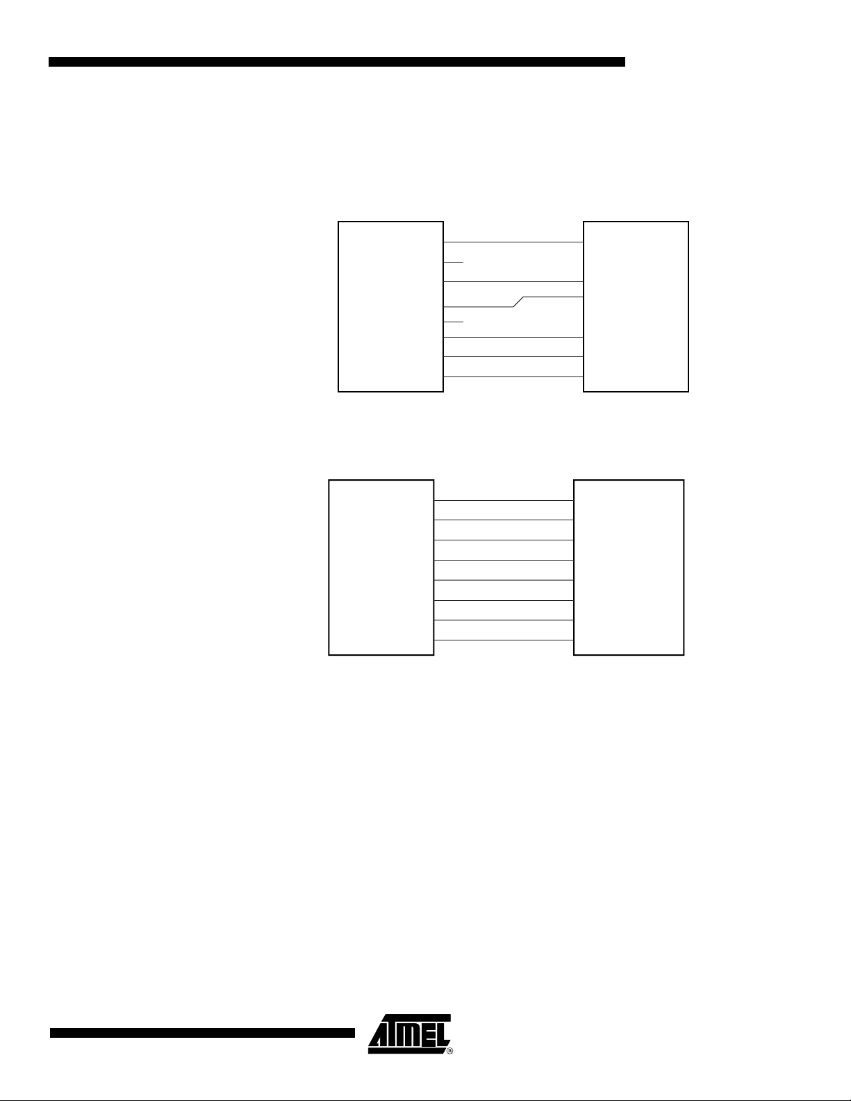
Figure 7-1. Separate or Common Reset Management
Reset
Controller
Reset
Controller
NTRST
NRST
AT91M55800A
(1) (2)
Reset
Controller
NTRST
NRST
AT91M55800A
14
Notes: 1. NRST and NTRST handling in Debug Mode during development.
2. NRST and NTRST handling during production.
AT91M55800A
1745D–ATARM–04-Nov-05
Page 15

In order to benefit the most regarding the separation of NRST and NTRST during the Debug
phase of development, the user must independently manage both signals as shown in example (1) of Figure 7-1 above. However, once Debug is completed, both signals are easily
managed together during production as shown in example (2) of Figure 7-1 above.
7.4.3 Watchdog Reset
The watchdog can be programmed to generate an internal reset. In this case, the reset has
the same effect as the NRST pin assertion, but the pins BMS and NTRI are not sampled. Boot
Mode and Tri-state Mode are not updated. If the NRST pin is asserted and the watchdog triggers the internal reset, the NRST pin has priority.
7.5 Emulation Functions
7.5.1 Tri-state Mode
The AT91M55800A provides a Tri-state Mode, which is used for debug purposes. This
enables the connection of an emulator probe to an application board without having to desolder the device from the target board. In Tri-state Mode, all the output pin drivers of the
AT91M55800A microcontroller are disabled.
To enter Tri-state Mode, the pin NTRI must be held low during the last 10 clock cycles before
the rising edge of NRST. For normal operation the pin NTRI must be held high during reset, by
a resistor of up to 400K Ohm.
AT91M55800A
NTRI is multiplexed with I/O line PA18 and USART 1 serial data transmit line TXD1.
Standard RS232 drivers generally contain internal 400K Ohm pull-up resistors. If TXD1 is connected to a device not including this pull-up, the user must make sure that a high level is tied
on NTRI while NRST is asserted.
7.5.2 JTAG/ICE Debug Mode
ARM Standard Embedded In-Circuit Emulation is supported via the JTAG/ICE port. It is connected to a host computer via an external ICE Interface. The JTAG/ICE debug mode is
enabled when JTAGSEL is low.
In ICE Debug Mode the ARM Core responds with a non-JTAG chip ID which identifies the core
to the ICE system. This is not JTAG compliant.
7.5.3 IEEE 1149.1 JTAG Boundary-scan
JTAG Boundary-scan is enabled when JTAGSEL is high. The functions SAMPLE, EXTEST
and BYPASS are implemented. There is no JTAG chip ID. The Special Function module provides a chip ID which is independent of JTAG.
It is not possible to switch directly between JTAG and ICE operations. A chip reset must be
performed (NRST and NTRST) after JTAGSEL is changed.
7.6 Memory Controller
The ARM7TDMI processor address space is 4G bytes. The memory controller decodes the
internal 32-bit address bus and defines three address spaces:
1745D–ATARM–04-Nov-05
• Internal memories in the four lowest megabytes
• Middle space reserved for the external devices (memory or peripherals) controlled by the
EBI
15
Page 16

7.6.1 Internal Memories
7.6.2 Boot Mode Select
• Internal peripherals in the four highest megabytes
In any of these address spaces, the ARM7TDMI operates in Little-Endian mode only.
The AT91M55800A microcontroller integrates an 8-Kbyte SRAM bank. This memory bank is
mapped at address 0x0 (after the remap command), allowing ARM7TDMI exception vectors
between 0x0 and 0x20 to be modified by the software. The rest of the bank can be used for
stack allocation (to speed up context saving and restoring), or as data and program storage for
critical algorithms. All internal memory is 32 bits wide and single-clock cycle accessible. Byte
(8-bit), half-word (16-bit) or word (32-bit) accesses are supported and are executed within one
cycle. Fetching Thumb or ARM instructions is supported and internal memory can store twice
as many Thumb instructions as ARM ones.
The ARM reset vector is at address 0x0. After the NRST line is released, the ARM7TDMI executes the instruction stored at this address. This means that this address must be mapped in
nonvolatile memory after the reset.
The input level on the BMS pin during the last 10 clock cycles before the rising edge of the
NRST selects the type of boot memory (see Table 7-2).
The pin BMS is multiplexed with the I/O line PB18 that can be programmed after reset like any
standard PIO line.
7.6.3 Remap Command
7.6.4 Abort Control
Table 7-2. Boot Mode Select
BMS Boot Mode
1 External 8-bit memory on NCS0
0 External 16-bit memory on NCS0
The ARM vectors (Reset, Abort, Data Abort, Prefetch Abort, Undefined Instruction, Interrupt,
Fast Interrupt) are mapped from address 0x0 to address 0x20. In order to allow these vectors
to be redefined dynamically by the software, the AT91M55800A microcontroller uses a remap
command that enables switching between the boot memory and the internal RAM bank
addresses. The remap command is accessible through the EBI User Interface, by writing one
in RCB of EBI_RCR (Remap Control Register). Performing a remap command is mandatory if
access to the other external devices (connected to chip selects 1 to 7) is required. The remap
operation can only be changed back by an internal reset or an NRST assertion.
The abort signal providing a Data Abort or a Prefetch Abort exception to the ARM7TDMI is
asserted when accessing an undefined address in the EBI address space.
No abort is generated when reading the internal memory or by accessing the internal peripherals, whether the address is defined or not.
16
AT91M55800A
1745D–ATARM–04-Nov-05
Page 17

7.7 External Bus Interface
The External Bus Interface handles the accesses between addresses 0x0040 0000 and
0xFFC0 0000. It generates the signals that control access to the external devices, and can
configure up to eight 16-Mbyte banks. In all cases it supports byte, half-word and word aligned
accesses.
For each of these banks, the user can program:
• Number of wait states
• Number of data float times (wait time after the access is finished to prevent any bus
contention in case the device is too long in releasing the bus)
• Data bus width (8-bit or 16-bit)
• With a 16-bit wide data bus, the user can program the EBI to control one 16-bit device
(Byte Access Select Mode) or two 8-bit devices in parallel that emulate a 16-bit memory
(Byte-write Access mode).
The External Bus Interface features also the Early Read Protocol, configurable for all the
devices, that significantly reduces access time requirements on an external device.
AT91M55800A
1745D–ATARM–04-Nov-05
17
Page 18

8. Peripherals
The AT91M55800A peripherals are connected to the 32-bit wide Advanced Peripheral Bus.
Peripheral registers are only word accessible – byte and half-word accesses are not supported. If a byte or a half-word access is attempted, the memory controller automatically
masks the lowest address bits and generates a word access.
Each peripheral has a 16-Kbyte address space allocated (the AIC only has a 4-Kbyte address
space).
8.1 Peripheral Registers
The following registers are common to all peripherals:
• Control Register – Write-only register that triggers a command when a one is written to the
corresponding position at the appropriate address. Writing a zero has no effect.
• Mode Register – read/write register that defines the configuration of the peripheral. Usually
has a value of 0x0 after a reset.
• Data Register – read and/or write register that enables the exchange of data between the
processor and the peripheral.
• Status Register – Read-only register that returns the status of the peripheral.
• Enable/Disable/Status Registers – shadow command registers. Writing a one in the Enable
Register sets the corresponding bit in the Status Register. Writing a one in the Disable
Register resets the corresponding bit and the result can be read in the Status Register.
Writing a bit to zero has no effect. This register access method maximizes the efficiency of
bit manipulation, and enables modification of a register with a single non-interruptible
instruction, replacing the costly read-modify-write operation.
Unused bits in the peripheral registers are shown as “–” and must be written at 0 for upward
compatibility. These bits read 0.
8.2 Peripheral Interrupt Control
The Interrupt Control of each peripheral is controlled from the status register using the interrupt mask. The status register bits are ANDed to their corresponding interrupt mask bits and
the result is then ORed to generate the Interrupt Source signal to the Advanced Interrupt
Controller.
The interrupt mask is read in the Interrupt Mask Register and is modified with the Interrupt
Enable Register and the Interrupt Disable Register. The enable/disable/status (or mask)
makes it possible to enable or disable peripheral interrupt sources with a non-interruptible single instruction. This eliminates the need for interrupt masking at the AIC or Core level in realtime and multi-tasking systems.
8.3 Peripheral Data Controller
An on-chip, 8-channel Peripheral Data Controller (PDC) transfers data between the on-chip
USARTs/SPI and the on and off-chip memories without processor intervention. One PDC
channel is connected to the receiving channel and one to the transmitting channel of each
USART and SPI.
The user interface of a PDC channel is integrated in the memory space of each peripheral. It
contains a 32-bit address pointer register and a 16-bit count register. When the programmed
data is transferred, an end of transfer interrupt is generated by the corresponding peripheral.
18
AT91M55800A
1745D–ATARM–04-Nov-05
Page 19

Most importantly, the PDC removes the processor interrupt handling overhead and significantly reduces the number of clock cycles required for a data transfer. It can transfer up to 64K
contiguous bytes. As a result, the performance of the microcontroller is increased and the
power consumption reduced.
8.4 System Peripherals
8.4.1 APMC: Advanced Power Management Controller
The AT91M55800A Advanced Power Management Controller allows optimization of power
consumption. The APMC enables/disables the clock inputs of most of the peripherals and the
ARM Core. Moreover, the main oscillator, the PLL and the analog peripherals can be put in
standby mode allowing minimum power consumption to be obtained. The APMC provides the
following operating modes:
• Normal: clock generator provides clock to the entire chip except the RTC.
• Wait mode: ARM Core clock deactivated
• Slow Clock mode: clock generator deactivated, master clock 32 kHz
• Standby mode: RTC active, all other clocks disabled
• Power down: RTC active, supply on the rest of the circuit deactivated
AT91M55800A
8.4.2 RTC: Real-time Clock
The AT91M55800A features a Real-time Clock (RTC) peripheral that is designed for very low
power consumption. It combines a complete time-of-day clock with alarm and a two-hundred
year Gregorian calendar, complemented by a programmable periodic interrupt.
The time and calendar values are coded in Binary-Coded Decimal (BCD) format. The time format can be 24-hour mode or 12-hour mode with an AM/PM indicator.
Updating time and calendar fields and configuring the alarm fields is performed by a parallel
capture on the 32-bit data bus. An entry control is performed to avoid loading registers with
incompatible BCD format data or with an incompatible date according to the current month/
year/century.
8.4.3 AIC: Advanced Interrupt Controller
The AIC has an 8-level priority, individually maskable, vectored interrupt controller, and drives
the NIRQ and NFIQ pins of the ARM7TDMI from:
• The external fast interrupt line (FIQ)
• The six external interrupt request lines (IRQ0 - IRQ5)
• The interrupt signals from the on-chip peripherals.
The AIC is largely programmable offering maximum flexibility, and its vectoring features
reduce the real-time overhead in handling interrupts.
The AIC also features a spurious vector, which reduces Spurious Interrupt handling to a minimum, and a protect mode that facilitates the debug capabilities.
8.4.4 PIO: Parallel I/O Controller
The AT91M55800A has 58 programmable I/O lines. 13 pins are dedicated as general-purpose
I/O pins. The other I/O lines are multiplexed with an external signal of a peripheral to optimize
the use of available package pins. The PIO lines are controlled by two separate and identical
1745D–ATARM–04-Nov-05
19
Page 20

PIO Controllers called PIOA and PIOB. The PIO controller enables the generation of an interrupt on input change and insertion of a simple input glitch filter on any of the PIO pins.
8.4.5 WD: Watchdog
The Watchdog is built around a 16-bit counter, and is used to prevent system lock-up if the
software becomes trapped in a deadlock. It can generate an internal reset or interrupt, or
assert an active level on the dedicated pin NWDOVF. All programming registers are password-protected to prevent unintentional programming.
8.4.6 SF: Special Function
The AT91M55800A provides registers which implement the following special functions.
• Chip identification
• RESET status
8.5 User Peripherals
8.5.1 USART: Universal Synchronous/
Asynchronous Receiver Transmitter
The AT91M55800A provides three identical, full-duplex, universal synchronous/asynchronous
receiver/transmitters.
Each USART has its own baud rate generator, and two dedicated Peripheral Data Controller
channels. The data format includes a start bit, up to 8 data bits, an optional programmable parity bit and up to 2 stop bits.
The USART also features a Receiver Timeout register, facilitating variable-length frame support when it is working with the PDC, and a Time-guard register, used when interfacing with
slow remote equipment.
8.5.2 TC: Timer Counter
The AT91M55800A features two Timer Counter blocks that include three identical 16-bit timer
counter channels. Each channel can be independently programmed to perform a wide range
of functions including frequency measurement, event counting, interval measurement, pulse
generation, delay timing and pulse-width modulation.
The Timer Counters can be used in Capture or Waveform mode, and all three counter channels can be started simultaneously and chained together.
8.5.3 SPI: Serial Peripheral Interface
The SPI provides communication with external devices in master or slave mode. It has four
external chip selects that can be connected to up to 15 devices. The data length is programmable, from 8- to 16-bit.
8.5.4 ADC: Analog-to-digital Converter
The two identical 4-channel 10-bit analog-to-digital converters (ADC) are based on a Successive Approximation Register (SAR) approach.
Each ADC has 4 analog input pins, AD0 to AD3 and AD4 to AD7, digital trigger input pins
AD0TRIG and AD1TRIG, and provides an interrupt signal to the AIC. Both ADCs share the
analog power supply pins VDDA and GNDA, and the input reference voltage pin ADVREF.
20
AT91M55800A
1745D–ATARM–04-Nov-05
Page 21

Each channel can be enabled or disabled independently, and has its own data register. The
ADC can be configured to automatically enter Sleep mode after a conversion sequence, and
can be triggered by the software, the Timer Counter, or an external signal.
8.5.5 DAC: Digital-to-analog Converter
Each DAC has an analog output pin, DA0 and DA1, and provides an interrupt signal to the AIC
DA0IRQ and DA1IRQ. Both DACs share the analog power supply pins VDDA and GNDA, and
the input reference DAVREF.
AT91M55800A
1745D–ATARM–04-Nov-05
21
Page 22

9. Memory Map
Figure 9-1. AT91M55800A Memory Map Before and after Remap Command
Before Remap After Remap
Address Function Size Abort Control
0xFFFFFFFF
0xFFC00000
0xFFBFFFFF
0x00400000
0x003FFFFF
On-chip
Peripherals
Reserved
On-chip RAM
4M Bytes
1M Byte
No
No
Address Function Size Abort Control
0xFFFFFFFF
0xFFC00000
0xFFBFFFFF
0x00400000
0x003FFFFF
On-chip
Peripherals
External
Devices
(up to 8)
Reserved
4M Bytes
Up to 8 Devices
Programmable Page Size
1, 4, 16, 64M Bytes
1M Byte No
No
Ye s
0x00300000
0x002FFFFF
0x00200000
0x001FFFFF
0x00100000
0x000FFFFF
0x00000000
Reserved
On-chip
Device
Reserved
On-chip
Device
External
Devices Selected
by NCS0
1M Byte
1M Byte
1M Byte
No
No
No
0x00300000
0x002FFFFF
0x00200000
0x001FFFFF
0x00100000
0x000FFFFF
0x00000000
Reserved
On-chip
Device
Reserved
On-chip
Device
On-chip RAM
1M Byte
1M Byte
1M Byte
No
No
No
22
AT91M55800A
1745D–ATARM–04-Nov-05
Page 23

10. Peripheral Memory Map
Figure 1. AT91M55800A Peripheral Memory Map
AT91M55800A
Address Peripheral Peripheral Name Size
0xFFFFFFFF
0xFFFFF000
0xFFFFBFFF
0xFFFF8000
0xFFFF7FFF
0xFFFF4000
0xFFFF3FFF
0xFFFF0000
0xFFFEFFFF
0xFFFEC000
0xFFFD7FFF
0xFFFD4000
0xFFFD3FFF
0xFFFD0000
0xFFFCBFFF
0xFFFC8000
0xFFFC7FFF
0xFFFC4000
0xFFFC3FFF
0xFFFC0000
0xFFFBFFFF
0xFFFBC000
0xFFFBBFFF
0xFFFB8000
0xFFFB7FFF
0xFFFB4000
0xFFFB3FFF
0xFFFB0000
0xFFFAFFFF
0xFFFAC000
0xFFFABFFF
0xFFFA8000
0xFFF03FFF
0xFFF00000
0xFFE03FFF
0xFFE00000
0xFFC00000
AIC
WD
APMC
PIO B
PIO A
TC 3,4,5
TC 0,1,2
USART2
USART1
USART0
SPI
RTC
ADC1
ADC0
DAC1
DAC0
SF
EBI
Advanced Interrupt Controller
Reserved
WatchdogTimer
Advanced Power
Management Controller
Parallel I/O Controller B
Parallel I/O Controller A
Reserved
Timer Counter Channels 3,4,5
Timer Counter Channels 0,1,2
Reserved
Universal Synchronous/
Asynchronous
Receiver/Transmitter 2
Universal Synchronous/
Asynchronous
Receiver/Transmitter 1
Universal Synchronous/
Asynchronous
Receiver/Transmitter 0
Serial Peripheral Interface
Real-time Clock
Analog-to-digital Converter 1
Analog-to-digital Converter 0
Digital-to-analog Converter 1
Digital-to-analog Converter 0
Reserved
Special Function
Reserved
External Bus Interface
Reserved
4K Bytes
16K Bytes
16K Bytes
16K Bytes
16K Bytes
16K Bytes
16K Bytes
16K Bytes
16K Bytes
16K Bytes
16K Bytes
16K Bytes
16K Bytes
16K Bytes
16K Bytes
16K Bytes
16K Bytes
16K Bytes
1745D–ATARM–04-Nov-05
23
Page 24

11. EBI: External Bus Interface
The EBI generates the signals that control the access to the external memory or peripheral
devices. The EBI is fully-programmable and can address up to 128M bytes. It has eight chip
selects and a 24-bit address bus.
The 16-bit data bus can be configured to interface with 8- or 16-bit external devices. Separate
read and write control signals allow for direct memory and peripheral interfacing.
The EBI supports different access protocols allowing single-clock cycle memory accesses.
The main features are:
• External memory mapping
• 8 active-low chip select lines
• 8- or 16-bit data bus
• Byte-write or byte-select lines
• Remap of boot memory
• Two different read protocols
• Programmable wait state generation
• External wait request
• Programmable data float time
The EBI User Interface is described on page 48.
24
AT91M55800A
1745D–ATARM–04-Nov-05
Page 25

11.1 External Memory Mapping
The memory map associates the internal 32-bit address space with the external 24-bit
address bus.
The memory map is defined by programming the base address and page size of the external
memories (see EBI User Interface registers EBI_CSR0 to EBI_CSR7). Note that A0 - A23 is
only significant for 8-bit memory; A1 - A23 is used for 16-bit memory.
If the physical memory device is smaller than the programmed page size, it wraps around and
appears to be repeated within the page. The EBI correctly handles any valid access to the
memory device within the page. (See Figure 11-1.)
In the event of an access request to an address outside any programmed page, an Abort signal is generated. Two types of Abort are possible: instruction prefetch abort and data abort.
The corresponding exception vector addresses are respectively 0x0000 000C and 0x0000
0010. It is up to the system programmer to program the error handling routine to use in case of
an Abort (see the ARM7TDMI datasheet for further information).
Figure 11-1. External Memory Smaller than Page Size
Memory
Map
1-Mbyte Device
1-Mbyte Device
1-Mbyte Device
1-Mbyte Device
Low
Low
Low
Low
AT91M55800A
Base + 4M Byte
Hi
Base + 3M Byte
Hi
Base + 2M Byte
Hi
Base + 1M Byte
Hi
Base
Repeat 3
Repeat 2
Repeat 1
1745D–ATARM–04-Nov-05
25
Page 26

11.2 EBI Pin Description
Name Description Type
A0 - A23 Address bus (output) Output
D0 - D15 Data bus (input/output) I/O
NCS0 - NCS7 Active low chip selects (output) Output
NRD Read Enable (output) Output
NWR0 - NWR1 Lower and upper write enable (output) Output
NOE Output enable (output) Output
NWE Write enable (output) Output
NUB, NLB Upper and lower byte-select (output) Output
NWAIT Wait request (input) Input
The following table shows how certain EBI signals are multiplexed:
Multiplexed Signals Functions
A0 NLB 8- or 16-bit data bus
NRD NOE Byte-write or byte-select access
NWR0 NWE Byte-write or byte-select access
NWR1 NUB Byte-write or byte-select access
26
AT91M55800A
1745D–ATARM–04-Nov-05
Page 27
11.3 Data Bus Width
AT91M55800A
A data bus width of 8 or 16 bits can be selected for each chip select. This option is controlled
by the DBW field in the EBI_CSR (Chip-select Register) for the corresponding chip select.
Figure 11-2 shows how to connect a 512K x 8-bit memory on NCS2.
Figure 11-2. Memory Connection for an 8-bit Data Bus
EBI
D0 - D7
D8 - D15
A1 - A18
A0
NWR1
NWR0
NRD
NCS2
D0 - D7
A1 - A18
A0
Write Enable
Output Enable
Memory Enable
Figure 11-3 shows how to connect a 512K x 16-bit memory on NCS2.
Figure 11-3. Memory Connection for a 16-bit Data Bus
EBI
D0 - D7
D8 - D15
A1 - A19
NLB
NUB High Byte Enable
NWE
NOE
NCS2
D0 - D7
D8 - D15
A0 - A18
Low Byte Enable
Write Enable
Output Enable
Memory Enable
11.4 Byte-write or Byte-select Access
Each chip select with a 16-bit data bus can operate with one of two different types of write
access:
• Byte-write Access supports two Byte-write and a single read signal.
• Byte-select Access selects upper and/or lower byte with two byte-select lines, and separate
read and write signals.
This option is controlled by the BAT field in the EBI_CSR (Chip-select Register) for the corresponding chip select.
Byte-write Access is used to connect 2 x 8-bit devices as a 16-bit memory page.
• The signal A0/NLB is not used.
• The signal NWR1/NUB is used as NWR1 and enables upper byte writes.
• The signal NWR0/NWE is used as NWR0 and enables lower byte writes.
• The signal NRD/NOE is used as NRD and enables half-word and byte reads.
Figure 11-4 shows how to connect two 512K x 8-bit devices in parallel on NCS2.
1745D–ATARM–04-Nov-05
27
Page 28
Figure 11-4. Memory Connection for 2 x 8-bit Data Busses
EBI
D0 - D7
D8 - D15
A1 - A19
A0
NWR1
NWR0
NRD
NCS2
D0 - D7
A0 - A18
Write Enable
Read Enable
Memory Enable
D8 - D15
A0 - A18
Write Enable
Read Enable
Memory Enable
Byte-select Access is used to connect 16-bit devices in a memory page.
• The signal A0/NLB is used as NLB and enables the lower byte for both read and write
operations.
• The signal NWR1/NUB is used as NUB and enables the upper byte for both read and write
operations.
• The signal NWR0/NWE is used as NWE and enables writing for byte or half word.
• The signal NRD/NOE is used as NOE and enables reading for byte or half word.
Figure 11-5 shows how to connect a 16-bit device with byte and half-word access (e.g. 16-bit
SRAM) on NCS2.
Figure 11-5. Connection for a 16-bit Data Bus with Byte and Half-word Access
EBI
D0 - D7
D8 - D15
A1 - A19
NLB
NUB High Byte Enable
NWE
NOE
NCS2
D0 - D7
D8 - D15
A0 - A18
Low Byte Enable
Write Enable
Output Enable
Memory Enable
28
AT91M55800A
1745D–ATARM–04-Nov-05
Page 29

AT91M55800A
Figure 11-6 shows how to connect a 16-bit device without byte access (e.g. Flash) on NCS2.
Figure 11-6. Connection for a 16-bit Data Bus Without Byte-write Capability.
11.5 Boot on NCS0
EBI
D0 - D7
D8 - D15
A1 - A19
NLB
NUB
NWE
NOE
NCS2
D0 - D7
D8 - D15
A0 - A18
Write Enable
Output Enable
Memory Enable
Depending on the device and the BMS pin level during the reset, the user can select either an
8-bit or 16-bit external memory device connected on NCS0 as the Boot Memory. In this case,
EBI_CSR0 (Chip-select Register 0) is reset at the following configuration for chip select 0:
• 8 wait states (WSE = 1, NWS = 7)
• 8-bit or 16-bit data bus width, depending on BMS
Byte access type and number of data float time are respectively set to Byte-write Access and
0. With a nonvolatile memory interface, any value can be programmed for these parameters.
Before the remap command, the user can modify the chip select 0 configuration, programming
the EBI_CSR0 with exact boot memory characteristics. The base address becomes effective
after the remap command, but the new number of wait states can be changed immediately.
This is useful if a boot sequence needs to be faster.
1745D–ATARM–04-Nov-05
29
Page 30
11.6 Read Protocols
The EBI provides two alternative protocols for external memory read access: standard and
early read. The difference between the two protocols lies in the timing of the NRD (read cycle)
waveform.
The protocol is selected by the DRP field in EBI_MCR (Memory Control Register) and is valid
for all memory devices. Standard read protocol is the default protocol after reset.
Note: In the following waveforms and descriptions, NRD represents NRD and NOE since the two sig-
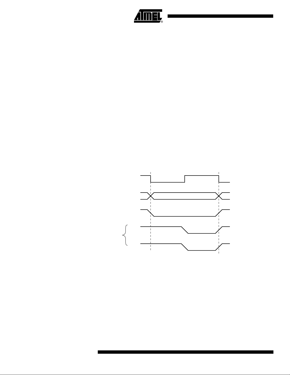
11.6.1 Standard Read Protocol
Standard read protocol implements a read cycle in which NRD and NWE are similar. Both are
active during the second half of the clock cycle. The first half of the clock cycle allows time to
ensure completion of the previous access as well as the output of address and NCS before the
read cycle begins.
During a standard read protocol, external memory access, NCS is set low and ADDR is valid
at the beginning of the access while NRD goes low only in the second half of the master clock
cycle to avoid bus conflict (see Figure 11-7). NWE is the same in both protocols. NWE always
goes low in the second half of the master clock cycle (see Figure 11-8).
Figure 11-7. Standard Read Protocol
nals have the same waveform. Likewise, NWE represents NWE, NWR0 and NWR1 unless
NWR0 and NWR1 are otherwise represented. ADDR represents A0 - A23 and/or A1 - A23.
11.6.2 Early Read Protocol
Early read protocol provides more time for a read access from the memory by asserting NRD
at the beginning of the clock cycle. In the case of successive read cycles in the same memory,
NRD remains active continuously. Since a read cycle normally limits the speed of operation of
the external memory system, early read protocol can allow a faster clock frequency to be
used. However, an extra wait state is required in some cases to avoid contentions on the
external bus.
MCK
ADDR
NCS
NRD
or
NWE
30
AT91M55800A
1745D–ATARM–04-Nov-05
Page 31
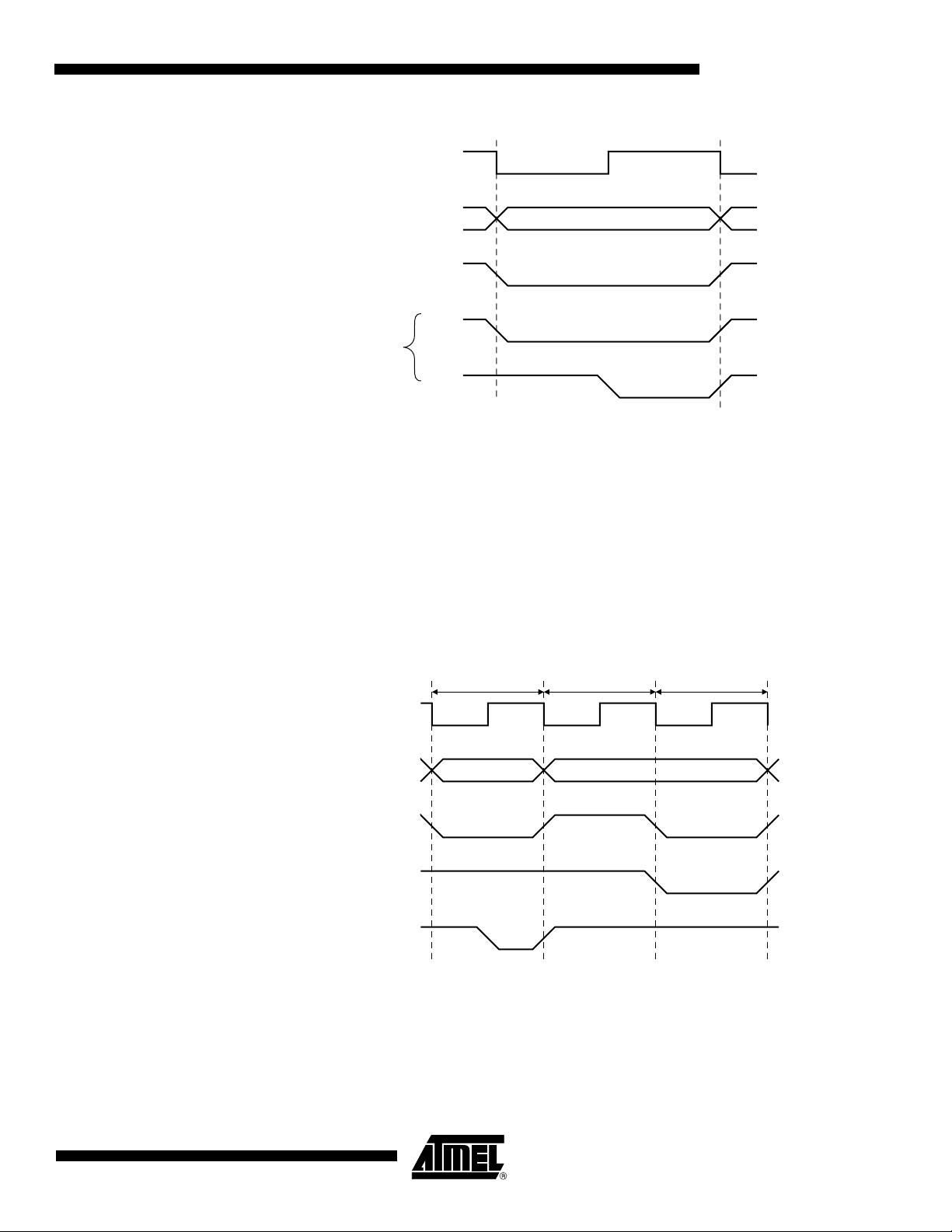
Figure 11-8. Early Read Protocol
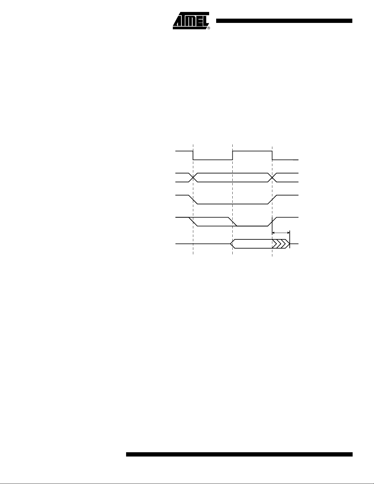
11.6.3 Early Read Wait State
In early read protocol, an early read wait state is automatically inserted when an external write
cycle is followed by a read cycle to allow time for the write cycle to end before the subsequent
read cycle begins (see Figure 11-9). This wait state is generated in addition to any other programmed wait states (i.e. data float wait).
AT91M55800A
MCK
ADDR
NCS
NRD
or
NWE
No wait state is added when a read cycle is followed by a write cycle, between consecutive
accesses of the same type or between external and internal memory accesses.
Early read wait states affect the external bus only. They do not affect internal bus timing.
Figure 11-9. Early Read Wait State
MCK
ADDR
NCS
NRD
NWE
Write Cycle
Early Read Wait
Read Cycle
1745D–ATARM–04-Nov-05
31
Page 32

11.7 Write Data Hold Time
During write cycles in both protocols, output data becomes valid after the falling edge of the
NWE signal and remains valid after the rising edge of NWE, as illustrated in the figure below.
The external NWE waveform (on the NWE pin) is used to control the output data timing to
guarantee this operation.
It is therefore necessary to avoid excessive loading of the NWE pins, which could delay the
write signal too long and cause a contention with a subsequent read cycle in standard
protocol.
Figure 11-10. Data Hold Time
MCK
ADDR
NWE
Data output
In early read protocol the data can remain valid longer than in standard read protocol due to
the additional wait cycle which follows a write access.
32
AT91M55800A
1745D–ATARM–04-Nov-05
Page 33

11.8 Wait States
The EBI can automatically insert wait states. The different types of wait states are listed below:
• Standard wait states
• Data float wait states
• External wait states
• Chip select change wait states
• Early read wait states (as described in Read Protocols)
11.8.1 Standard Wait States
Each chip select can be programmed to insert one or more wait states during an access on
the corresponding device. This is done by setting the WSE field in the corresponding
EBI_CSR. The number of cycles to insert is programmed in the NWS field in the same
register.
Below is the correspondence between the number of standard wait states programmed and
the number of cycles during which the NWE pulse is held low:
AT91M55800A
0 wait states 1/2 cycle
1 wait state 1 cycle
For each additional wait state programmed, an additional cycle is added.
Figure 11-11. One Wait State Access
1 Wait State Access
MCK
ADDR
NCS
NWE
NRD
Notes: 1. Early Read Protocol
2. Standard Read Protocol
(1)
(2)
11.8.2 Data Float Wait State
Some memory devices are slow to release the external bus. For such devices it is necessary
to add wait states (data float waits) after a read access before starting a write access or a read
access to a different external memory.
The Data Float Output Time (t
field of the EBI_CSR register for the corresponding chip select. The value (0 - 7 clock cycles)
1745D–ATARM–04-Nov-05
) for each external memory device is programmed in the TDF
DF
33
Page 34
indicates the number of data float waits to be inserted and represents the time allowed for the
data output to go high impedance after the memory is disabled.
Data float wait states do not delay internal memory accesses. Hence, a single access to an
external memory with long t
will not slow down the execution of a program from internal
DF
memory.
The EBI keeps track of the programmed external data float time during internal accesses, to
ensure that the external memory system is not accessed while it is still busy.
Internal memory accesses and consecutive accesses to the same external memory do not
have added Data Float wait states.
Figure 11-12. Data Float Output Time
MCK
ADDR
NCS
11.8.3 External Wait
NRD
D0-D15
Notes: 1. Early Read Protocol
2. Standard Read Protocol
(1) (2)
t
DF
The NWAIT input can be used to add wait states at any time. NWAIT is active low and is
detected on the rising edge of the clock.
If NWAIT is low at the rising edge of the clock, the EBI adds a wait state and changes neither
the output signals nor its internal counters and state. When NWAIT is de-asserted, the EBI finishes the access sequence.
The NWAIT signal must meet setup and hold requirements on the rising edge of the clock.
34
AT91M55800A
1745D–ATARM–04-Nov-05
Page 35
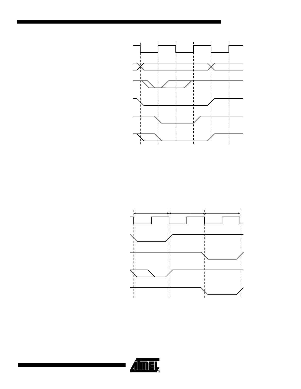
Figure 11-13. External Wait
MCK
ADDR
NWAIT
NCS
NWE
AT91M55800A
Notes: 1. Early Read Protocol
2. Standard Read Protocol
11.8.4 Chip Select Change Wait States
A chip select wait state is automatically inserted when consecutive accesses are made to two
different external memories (if no wait states have already been inserted). If any wait states
have already been inserted, (e.g., data float wait) then none are added.
Figure 11-14. Chip Select Wait
NRD
MCK
NCS1
NCS2
NRD
(1)
(1) (2)
(2)
Mem 1 Chip Select Wait Mem 2
1745D–ATARM–04-Nov-05
NWE
Notes: 1. Early Read Protocol
2. Standard Read Protocol
35
Page 36

11.9 Memory Access Waveforms
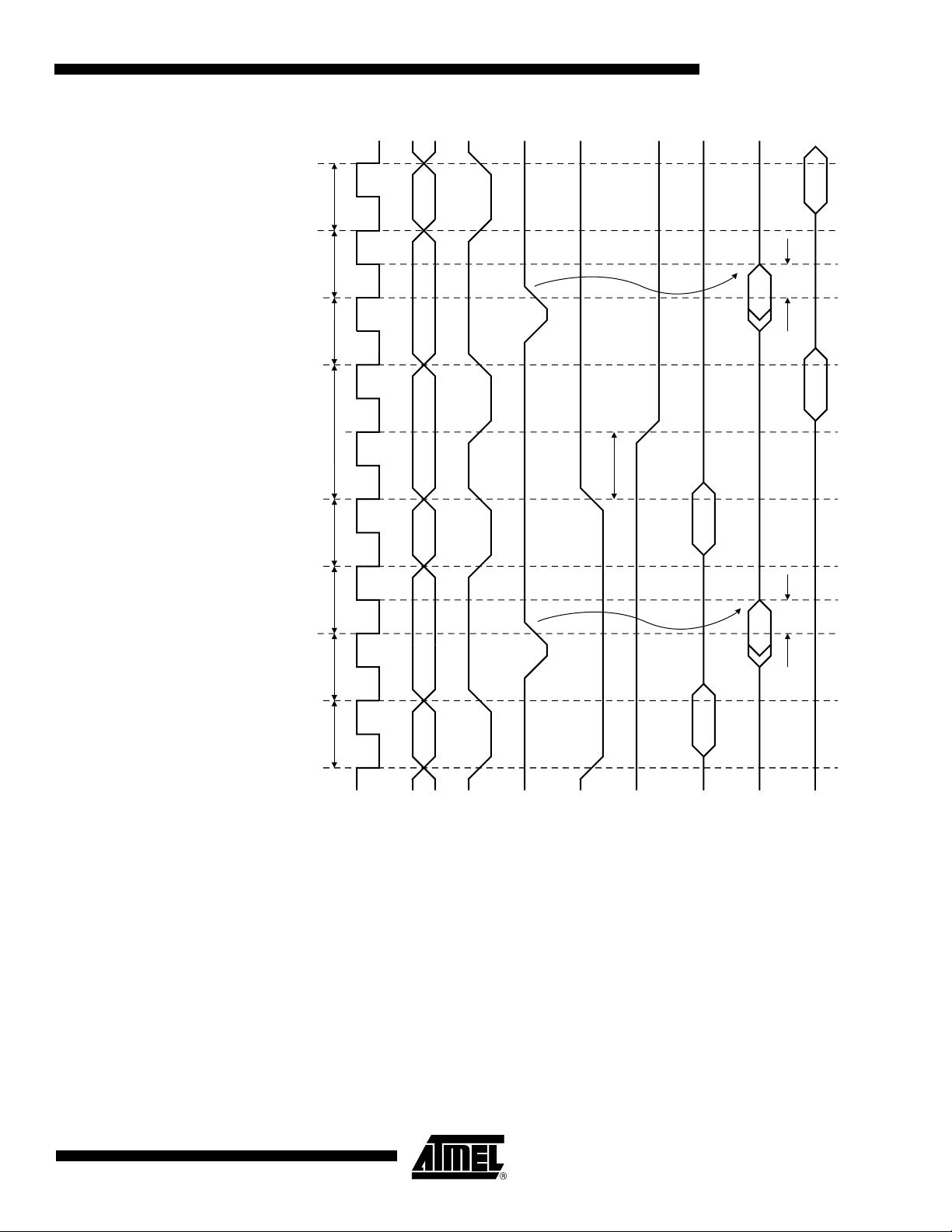
Figure 11-15 through Figure 11-18 show examples of the two alternative protocols for external
memory read access.
Figure 11-15. Standard Read Protocol with no t
Read Mem 2
Write Mem 2
Read Mem 2
DF
Chip Select
Change Wait
WHDX
t
WHDX
t
Read Mem 1
Write Mem 1
Read Mem 1
MCK
A0 - A23
NRD
NWE
NCS1
NCS2
D0 - D15 (Mem 1)
D0 - D15 (AT91)
D0 - D15 (Mem 2)
36
AT91M55800A
1745D–ATARM–04-Nov-05
Page 37
AT91M55800A
Figure 11-16. Early Read Protocol with no t
Read
Mem 2
Wait Cycle
Early Read
Write
Mem 2
Read
Mem 2
Read
Mem 1
DF
Chip Select
Change Wait
WHDX
Long t
WHDX
Long t
Wait Cycle
Early Read
Write
Mem 1
Read
Mem 1
MCK
A0 - A23
NRD
NWE
NCS1
NCS2
D0 - D15 (Mem 1)
D0 - D15 (AT91)
D0 - D15 (Mem 2)
1745D–ATARM–04-Nov-05
37
Page 38

Figure 11-17. Standard Read Protocol with t
Write
Mem 2
Write
Mem 2
Write
Mem 2
DF
Data
Read Mem 2
Read
Mem 2
Data
Read Mem 1
Write
Mem 1
Data
Float Wait
Float Wait
Float Wait
DF
t
DF
t
WHDX
t
DF
t
38
AT91M55800A
Read Mem 1
MCK
A0 - A23
NRD
NWE
NCS1
NCS2
D0 - D15 (Mem 1)
D0 - D15 (AT91)
1745D–ATARM–04-Nov-05
D0 - D15 (Mem 2)
Page 39
AT91M55800A
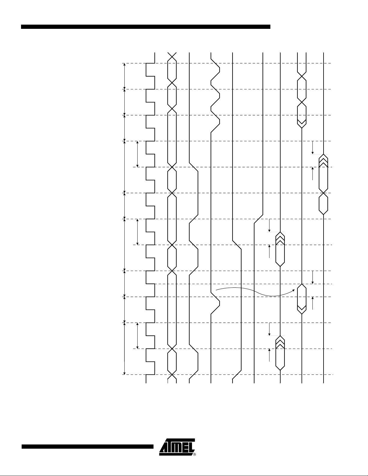
Figure 11-18. Early Read Protocol with t
Write
Mem 2
Write
Mem 2
Write
Mem 2
Data
Float Wait
Read Mem 2
Read
Mem 2
DF
DF
t
Data
Read Mem 1
Early
Read Wait
Write
Mem 1
Data
Read Mem 1
Float Wait
Float Wait
MCK
A0 - A23
NRD
NWE
NCS1
NCS2
DF
t
WHDX
t
DF
t
1745D–ATARM–04-Nov-05
D0 - D15 (Mem 1)
D0 - D15 (AT91)
D0 - D15 (Mem 2)
39
Page 40

Figure 11-19 through Figure 11-25 show the timing cycles and wait states for read and write
access to the various AT91M55800A external memory devices. The configurations described
are as follows:
Table 11-1. Memory Access Waveforms
Figure Number Number of Wait States Bus Width Size of Data Transfer
11-19 0 16 Word
11-20 1 16 Word
11-21 1 16 Half-word
11-22 0 8 Word
11-23 1 8 Half-word
11-24 1 8 Byte
11-25 0 16 Byte
40
AT91M55800A
1745D–ATARM–04-Nov-05
Page 41

Figure 11-19. 0 Wait States, 16-bit Bus Width, Word Transfer
MCK
AT91M55800A
READ ACCESS
· Standard Protocol
· Early Protocol
A1 - A23
NCS
NLB
NUB
NRD
D0 - D15
Internal Bus
ADDR
ADDR+1
B2B1 B
X X B2 B
1
4 B3
B4 B3 B2 B
1
WRITE ACCESS
· Byte Write/
Byte Select Option
1745D–ATARM–04-Nov-05
NRD
NWE
B2 B
1
B2 B1
B4 B
B
3 D0 - D15
B
3 D0 - D15
4
41
Page 42

Figure 11-20. 1 Wait State, 16-bit Bus Width, Word Transfer
1 Wait State 1 Wait State
MCK
READ ACCESS
· Standard Protocol
A1 - A23
NCS
NLB
NUB
NRD
D0 - D15
Internal Bus
ADDR
B2 B1
X X B
2 B1
ADDR+1
B4 B3
B4 B3 B2 B
1
· Early Protocol
WRITE ACCESS
· Byte Write/
Byte Select Option
NRD
D0 - D15
NWE
D0 - D15
B2B
B4B
B4B
3
3
B2B
1
1
42
AT91M55800A
1745D–ATARM–04-Nov-05
Page 43

Figure 11-21. 1 Wait State, 16-bit Bus Width, Half-word Transfer
1 Wait State
MCK
A1 - A23
NCS
NLB
NUB
READ ACCESS
· Standard Protocol
NRD
AT91M55800A
· Early Protocol
WRITE ACCESS
· Byte Write/
Byte Select Option
D0 - D15
Internal Bus
NRD
D0 - D15
NWE
D0 - D15
B2 B
B2 B
B2 B
1
X X B2 B
1
1
1
1745D–ATARM–04-Nov-05
43
Page 44

Figure 11-22. 0 Wait States, 8-bit Bus Width, Word Transfer
MCK
A0 - A23
NCS
READ ACCESS
· Standard Protocol
NRD
D0 - D15
Internal Bus
· Early Protocol
NRD
D0 - D15
ADDR
X B
1
X X X B
X B
1
ADDR+1
1
X B
2
X X B2 B
X B
2
ADDR+2 ADDR+3
X B
3
1
X B3 B2 B
X B
3
1
X B
4
B4 B3 B2 B
X B
4
1
WRITE ACCESS
NWR0
NWR1
D0 - D15
X B
1
X B
2
X B
3
X B
4
44
AT91M55800A
1745D–ATARM–04-Nov-05
Page 45

Figure 11-23. 1 Wait State, 8-bit Bus Width, Half-word Transfer
AT91M55800A
MCK
A0 - A23
NCS
READ ACCESS
· Standard Protocol
NRD
D0 - D15
Internal Bus
· Early Protocol
NRD
1 Wait State
ADDR
X B
X X X B
1
1 Wait State
1
ADDR+1
X B
2
X X B2 B
1
D0 - D15
WRITE ACCESS
NWR0
NWR1
D0 - D15
X B
X B
1
1
X B
X B
2
2
1745D–ATARM–04-Nov-05
45
Page 46

Figure 11-24. 1 Wait State, 8-bit Bus Width, Byte Transfer
1 Wait State
MCK
A0 - A23
NCS
READ ACCESS
· Standard Protocol
NRD
· Early Protocol
WRITE ACCESS
D0-D15
Internal Bus
NRD
D0 - D15
NWR0
NWR1
D0-D15
X B
X B
XB1
X X X B
1
1
1
46
AT91M55800A
1745D–ATARM–04-Nov-05
Page 47

Figure 11-25. 0 Wait States, 16-bit Bus Width, Byte Transfer
MCK
X X X
A1-A23
ADDR
0 ADDR X X X 0
AT91M55800A
Internal Address
READ ACCESS
·
Standard Protocol
Internal Bus
·
Early Protocol
NCS
NLB
NUB
NRD
D0-D15
NRD
ADDR X X X 0 ADDR X X X 1
X B
1
X X X B
1
B2X
X X B2X
WRITE ACCESS
·
Byte Write Option
·
Byte Select Option
1745D–ATARM–04-Nov-05
D0-D15
NWR0
NWR1
D0-D15
NWE
XB
B1B
1
1
B2X
B2B
2
47
Page 48

11.10 EBI User Interface
The EBI is programmed using the registers listed in the table below. The Remap Control Register (EBI_RCR) controls exit from Boot Mode (see Section 11.5 ”Boot on NCS0” on page 29)
The Memory Control Register (EBI_MCR) is used to program the number of active chip
selects and data read protocol. Eight Chip-select Registers (EBI_CSR0 to EBI_CSR7) are
used to program the parameters for the individual external memories. Each EBI_CSR must be
programmed with a different base address, even for unused chip selects.
Base Address: 0xFFE00000 (Code Label EBI_BASE)
Table 11-2. EBI Memory Map
Offset Register Name Access Reset State
0x00 Chip-select Register 0 EBI_CSR0 Read/Write
0x04 Chip-select Register 1 EBI_CSR1 Read/Write 0x10000000
0x08 Chip-select Register 2 EBI_CSR2 Read/Write 0x20000000
0x0C Chip-select Register 3 EBI_CSR3 Read/Write 0x30000000
0x10 Chip-select Register 4 EBI_CSR4 Read/Write 0x40000000
0x14 Chip-select Register 5 EBI_CSR5 Read/Write 0x50000000
0x18 Chip-select Register 6 EBI_CSR6 Read/Write 0x60000000
0x1C Chip-select Register 7 EBI_CSR7 Read/Write 0x70000000
0x20 Remap Control Register EBI_RCR Write-only –
0x24 Memory Control Register EBI_MCR Read/Write 0
Notes: 1. 8-bit boot (if BMS is detected high)
2. 16-bit boot (if BMS is detected low)
0x0000203E
0x0000203D
(1)
(2)
48
AT91M55800A
1745D–ATARM–04-Nov-05
Page 49

AT91M55800A
11.10.1 EBI Chip Select Register Register Name: EBI_CSR0 - EBI_CSR7 Access Type: Read/Write Reset Value: See Table 11-2 Absolute Address: 0xFFE00000 - 0xFFE0001C
31 30 29 28 27 26 25 24
BA
23 22 21 20 19 18 17 16
BA ––––
15 14 13 12 11 10 9 8
––CSENBAT TDF PAGES
76543210
PAGES – WSE NWS DBW
• DBW: Data Bus Width
Code Label
DBW Data Bus Width
0 0 Reserved –
EBI_DBW
0 1 16-bit data bus width EBI_DBW_16
1 0 8-bit data bus width EBI_DBW_8
1 1 Reserved –
• NWS: Number of Wait States
This field is valid only if WSE is set.
NWS Number of Standard Wait States
0 0 0 1 EBI_NWS_1
0 0 1 2 EBI_NWS_2
0 1 0 3 EBI_NWS_3
0 1 1 4 EBI_NWS_4
1 0 0 5 EBI_NWS_5
1 0 1 6 EBI_NWS_6
1 1 0 7 EBI_NWS_7
1 1 1 8 EBI_NWS_8
• WSE: Wait State Enable (Code Label EBI_WSE)
0 = Wait state generation is disabled. No wait states are inserted.
1 = Wait state generation is enabled.
Code Label
EBI_NWS
1745D–ATARM–04-Nov-05
49
Page 50

• PAGES: Page Size
Code Label
PAGES Page Size Active Bits in Base Address
0 0 1M Byte 12 Bits (31-20) EBI_PAGES_1M
0 1 4M Bytes 10 Bits (31-22) EBI_PAGES_4M
1 0 16M Bytes 8 Bits (31-24) EBI_PAGES_16M
1 1 64M Bytes 6 Bits (31-26) EBI_PAGES_64M
EBI_PAGES
• TDF: Data Float Output Time
Code Label
TDF Number of Cycles Added after the Transfer
0 0 0 0 EBI_TDF_0
0 0 1 1 EBI_TDF_1
0 1 0 2 EBI_TDF_2
0 1 1 3 EBI_TDF_3
1 0 0 4 EBI_TDF_4
1 0 1 5 EBI_TDF_5
1 1 0 6 EBI_TDF_6
1 1 1 7 EBI_TDF_7
EBI_TDF
• BAT: Byte Access Type
Code Label
BAT Selected BAT
0 Byte-write access type EBI_BAT_BYTE_WRITE
1 Byte-select access type EBI_BAT_BYTE_SELECT
EBI_BAT
• CSEN: Chip Select Enable (Code Label EBI_CSEN)
0 = Chip select is disabled.
1 = Chip select is enabled.
• BA: Base Address (Code Label EBI_BA)
These bits contain the highest bits of the base address. If the page size is larger than 1M byte, the unused bits of the base
address are ignored by the EBI decoder.
50
AT91M55800A
1745D–ATARM–04-Nov-05
Page 51

AT91M55800A
11.10.2 EBI Remap Control Register Register Name: EBI_RCR Access Type: Write-only Absolute Address: 0xFFE00020 Offset: 0x20
31 30 29 28 27 26 25 24
––––––––
23 22 21 20 19 18 17 16
––––––––
15 14 13 12 11 10 9 8
––––––––
76543210
–––––––RCB
• RCB: Remap Command Bit (Code Label EBI_RCB)
0 = No effect.
1 = Cancels the remapping (performed at reset) of the page zero memory devices.
11.10.3 EBI Memory Control Register Register Name: EBI_MCR Access Type: Read/Write Reset Value: 0 Absolute Address: 0xFFE00024 Offset: 0x24
31 30 29 28 27 26 25 24
––––––––
23 22 21 20 19 18 17 16
––––––––
15 14 13 12 11 10 9 8
––––––––
76543210
–––DRP––––
• DRP: Data Read Protocol
Code Label
DRP Selected DRP
0 Standard read protocol for all external memory devices enabled EBI_DRP_STANDARD
EBI_DRP
1 Early read protocol for all external memory devices enabled EBI_DRP_EARLY
1745D–ATARM–04-Nov-05
51
Page 52

12. APMC: Advanced Power Management Controller
The AT91M55800A features an Advanced Power Management Controller, which optimizes
both the power consumption of the device and the complete system. The APMC controls the
clocking elements such as the oscillators and the PLL, the core and the peripheral clocks, and
has the capability to control the system power supply.
Main Power is used throughout this document to identify the voltages powering the
AT91M55800A and other components of the system, with the exception of the Battery Backup
voltage, which is applied to the VDDBU. Main Power supplies VDDIO, VDDCORE and, if
required, the analog voltage VDDA. A battery or battery capacitor generally supplies the Battery Backup Power.
The APMC consists of the following elements:
• The RTC Oscillator, which provides the Slow Clock at 32768 Hz.
• The Main Oscillator, which provides a clock that depends on the frequency of the crystal
connected to the XIN and XOUT pins.
• The Phase Lock Loop.
• The ARM Core Clock Controller, which allows entry to the Idle Mode.
• The Peripheral Clock Controller, which conserves the power consumption of unused
peripherals.
• The Master Clock Output Controller.
• The Shut-down Logic, which controls the Main Power.
Figure 12-1. APMC Module
WAKEUP
NRSTBU
XIN32
XOUT32
XIN
XOUT
Reset Control
VDDBU
VDDIO/VDDCORE
RTC
OSC
Advanced Peripheral Bus
PLL Main OSC
Shut-down
Logic
PLL TimerOSC Timer
RTC
Alarm
(1)
Device
Clock
Control
APMC
IRQ
Control
SHDN
Slow Clock_SLCK
Arm Clock
0
Peripheral Clocks
n
ARM Interrupt (IRQ and FIQ)
SLCKIRQ
APMCIRQ
52
Note: The RTC peripheral is described in a separate section.
AT91M55800A
1745D–ATARM–04-Nov-05
Page 53

12.1 Operating Modes
AT91M55800A
Five operating modes are supported by the APMC and offer different power consumption levels and event response latency times.
•Normal Mode:
The Main Power supply is switched on; the ARM Core Clock is enabled and the peripheral
clocks are enabled according to the application requirements.
• Idle Mode:
The Main Power is switched on; the ARM Core Clock is disabled and waiting for the next
interrupt (or a main reset); the peripheral clocks are enabled according to the application
requirements and the PDC transfers are still possible.
• Slow Clock Mode:
Similar to Normal Mode, but the Main Oscillator and the PLL are switched off to save
power; the device core and peripheral run in Slow Clock Mode; Note that Slow Clock
Mode is the mode selected after the reset.
• Standby Mode:
A combination of the Slow Clock Mode and the Idle Mode, which enables the processor to
respond quickly to a wake-up event by keeping very low power consumption.
• Power-down Mode:
The Main Power supply is turned off at the external power source until a programmable
edge on the wake-up signal or a programmable RTC Alarm occurs.
1745D–ATARM–04-Nov-05
53
Page 54

Figure 12-2. APMC Block Diagram
WAKEUP
WKEDG
NRSTBU
XIN32
XOUT32
Edge Detector
Backup
Reset
WKACKC
Reset
Control
RTC
Oscillator
ALWKEN
ALSHEN
SHDALC
Backup Reset
Slow Clock
WKACKS
Wake-up
Acknowledge
Alarm
Shut-down
Alarm
RTC Alarm
Shut-down
Alarm
Output
Controller
RTC
SHDALS
SHDN
(1)
Battery Power
VDDBU
XOUT
NIRQ
NFIQ
XIN
APMC_SCDR
Set
IDLE MODE
FF
Clear
MOSCEN
Main
Oscillator
MOSCBYP
APMC_SCSR
ARM7TDMI
Clock
MUL
PLL
MCK (Master Clock)
APMC_PCER
APMC_PCDR
APMC_PCSR
CSS
Prescaler
Peripheral Clocks
Main Power
VDDIO
VDDCORE
PRES
MCKODS
MCKO
54
Note: 1. The RTC is described in another chapter
AT91M55800A
1745D–ATARM–04-Nov-05
Page 55

12.2 Slow Clock Generator
The AT91M55800A has a very low power 32 kHz oscillator powered by the backup battery
voltage supplied on the VDDBU pins. The XIN32 and XOUT32 pins must be connected to a
32768 Hz crystal. The oscillator has been especially designed to connect to a 6 pF typical load
capacitance crystal and does not require any external capacitor, as it integrates the XIN32 and
XOUT32 capacitors to ground. For a higher typical load capacitance, two external capacitances must be wired as shown in Figure 12-3:
Figure 12-3. Higher Typical Load Capacitance
12.2.1 Backup Reset Controller
The backup reset controller initializes the logic supplied by the backup battery power. A simple
RC circuit connected to the NRSTBU pin provides a power-on reset signal to the RTC and the
shutdown logic. When the reset signal increases and as the startup time of the 32 kHz oscilla
tor is around 300 ms, the AT91M55800A maintains the internal backup reset signal for 32768
oscillator clock cycles in order to guarantee the backup power supplied logic does not operate
before the oscillator output is stabilized.
Alternatively, a reset supervisor can be connected to the NRSTBU pin in place of the RC.
XIN32 XOUT32 GNDPLL
C
C
L1
L2
AT91M55800A
-
12.2.2 Slow Clock
The Slow Clock is the only clock considered permanent in an AT91M55800A-based system
and is essential in the operations of the APMC (Advanced Power Management Controller). In
any use-case, a 32768 Hz crystal must be connected to the XIN32 and XOUT32 pins in order
to ensure that the Slow Clock is present.
1745D–ATARM–04-Nov-05
55
Page 56

12.3 Clock Generator
12.3.1 Main Oscillator
The clock generator consists of the main oscillator, the PLL and the clock selection logic with
its prescaler. It aims at selecting the Master Clock, called MCK throughout this datasheet. The
clock generator also contains the circuitry needed to drive the MCKO pin with the master clock
signal.
The Main Oscillator is designed for a 3 to 20 MHz fundamental crystal. The typical crystal connection is illustrated in Figure 12-4. The 1 kΩ resistor is only required for crystals with
frequencies lower than 8 MHz. The oscillator contains 25 pF capacitances on each XIN and
XOUT pin. Consequently, CL1 and CL2 can be removed when a crystal with a load capacitance of 12.5 pF is used.
Figure 12-4. Typical Crystal Connection of Main Oscillator
XIN XOUT GNDPLL
1KΩ
12.3.2 Phase Lock Loop
C
C
L1
L2
The Main Oscillator can be bypassed if the MOSCBYP bit in the Clock Generator Mode Register (APMC_CGMR) is set to 1. In this case, any frequency (up to the maximum specified in the
electrical characteristics datasheet) can be input on the XIN pin. If the PLL is used, a minimum
input frequency is required.
To minimize the power required to start up the system, the Main Oscillator is disabled after the
reset. The software can deactivate the Main Oscillator to reduce the power consumption by
clearing the MOSCEN bit in APMC_CGMR. The MOSCS (Main Oscillator Status) bit in
APMC_SR is automatically cleared, indicating that the Main Oscillator is off.
Writing the MOSCEN bit in APMC_CGMR reactivates the Main Oscillator and loads the value
written in the OSCOUNT field in APMC_CGMR in the oscillator counter. Then, the oscillator
counter decrements every 8 clock cycles and when it reaches 0, the MOSCS bit is set and can
provide an interrupt.
The Main Oscillator output signal feeds the phase lock loop, which aims at multiplying the frequency of its input signal by a number up to 64. This number is programmed in the MUL field
of APMC_CGMR and the multiplication ratio is the programmed value plus one (MUL+1). If a
null value is programmed into MUL, the PLL is automatically disabled to save power.
The PLL is disabled at reset to minimize the power consumption.
A start-up sequence must be executed to enable the PLL if it is disabled. This sequence is
started by writing a new MUL value in APMC_CGMR. This automatically clears the LOCK bit
56
AT91M55800A
1745D–ATARM–04-Nov-05
Page 57

12.3.3 PLL Filter
AT91M55800A
in APMC_SR and loads the PLL counter with the value programmed in the PLLCOUNT field.
Then, the PLL counter decrements at each Slow Clock cycle.
Note: Programming one in PLLCOUNT is the minimum allowed and guarantees at least 2 Slow Clock
cycles before the lock bit is set. Programming n in PLLCOUNT guarantees (n+1) the delay of
Slow Clock cycles. When the PLL Counter reaches 0, the LOCK bit in APMC_SR is set and can
cause an interrupt. Programming MUL or PLLCOUNT before the LOCK bit is set may lead to
unpredictable behavior.
If the PLL multiplication is changed while the PLL is already active, the LOCK bit in APMC_SR
is automatically cleared and the same sequence is restarted. The PLL is automatically
bypassed while the frequency is changing (while LOCK is 0). If the Main Oscillator is reacti
vated at the same time the PLL is enabled, the LOCK bit is set only when both the Main
Oscillator and the PLL are stabilized.
The Phase Lock Loop has a dedicated PLLRC pin which must connect with an appropriate
second order filter made up of one resistor and two capacitors. If the integrated PLL is not
used, it can remain disabled. The PLLRC pin must be grounded if the resistor and the capaci
tors need to be saved. The following figure shows a typical filter connection.
Figure 12-5. Typical Filter Connection
PLLRC
-
-
In order to obtain optimal results with a 16 MHz input frequency and a 32 MHz output frequency, the typical component values for the PLL filter are:
R = 287Ω - C1 = 680 nF - C2 = 68 nF
The lock time with these values is about 3.5 µs in this example.
12.3.4 Master Clock Selection
The MCK (Master Clock) can be selected through the CSS field in APMC_CGMR between the
Slow Clock, the output of the Main Oscillator or the output of the PLL.
The following CSS field definitions are forbidden and the write operations are not taken into
account by the APMC:
• deselect the Slow Clock if the Main Oscillator is disabled or its output is not stabilized
• disable the PLL without having first selected the Slow Clock or the Main Oscillator clock
• select the PLL clock and, in the same register, write disable the PLL
• select either the Main Oscillator or the PLL clocks and, in the same register, write disable
the Main Oscillator
• disable the Main Oscillator without having first selected the Slow Clock
This clock switch is performed in some Slow Clocks and PLLs or Main Oscillator clock cycles
as described in the state machine diagram below:
GNDPLL
C
R
C
1
2
1745D–ATARM–04-Nov-05
57
Page 58

Figure 12-6. Clock Switch
12.3.5 Slow Clock Interrupt
The APMC also features the Slow Clock interrupt, allowing the user to detect when the Master
Clock is actually switched to the Slow Clock. Switching from the Slow Clock to a higher frequency is generally performed safely, as the processor is running slower than the target
frequency. However, switching from a high frequency to the Slow Clock requires the high frequency to be valid during the switch time. The Slow Clock interrupt permits the user to know
exactly when the switch has been achieved, thus, when the Main Oscillator or the PLL can be
disabled.
5 SLCK Cycles
PLL Clock Mode
7 SLCK Cycles
+
3 PLL Clock Cycles
Slow Clock Mode
4 SLCK Cycles
+
3 PLL Clock Cycles
5 SLCK Cycles
3 PLL Clock Cycles
4 SLCK Cycles
3 Oscillator Clock Cycles
3 SLCK Cycles
3 Oscillator Clock Cycles
+
+
+
5 SLCK Cycles
Oscillator Clock Mode
12.3.6 Prescaler
The prescaler is the last stage to provide the master clock. It permits the selected clock to be
divided by a power of 2 between 1 and 64. The default value is 1 after the reset. The prescaler
allows the microcontroller operating frequency to reach down to 512 Hz.
Precautions must be taken when defining a master clock lower than the Slow Clock, as some
peripherals (RTC and APMC) can still operate at Slow Clock frequency. In this case, access to
the peripheral registers that are updated at 32 kHz cannot be ensured.
12.3.7 Master Clock Output
The Master Clock can be output to the MCKO pad. The MCKO pad can be tri-stated to minimize power consumption by setting the bit MCKODS (Master Clock Output Disable) in
APMC_CGMR (default is MCKO enabled).
58
AT91M55800A
1745D–ATARM–04-Nov-05
Page 59

12.4 System Clock
The AT91M55800A has only one system clock: the ARM Core clock. It can be enabled and
disabled by writing to the System Clock Enable (APMC_SCER) and System Clock Disable
Registers (APMC_SCDR). The status of the ARM Core clock (at least for debug purposes)
can be read in the System Clock Status Register (APMC_SCSR).
The ARM Core clock is enabled after a reset and is automatically re-enabled by any enabled
interrupt.
When the ARM Core clock is disabled, the current instruction is finished before the clock is
stopped.
Note: Stopping the ARM Core does not prevent PDC transfers.
12.5 Peripheral Clocks
Each peripheral clock integrated in the AT91M55800A can be individually enabled and disabled by writing to the Peripheral Clock Enable (APMC_PCER) and Peripheral Clock Disable
(APMC_PCDR) Registers. The status of the peripheral clocks can be read in the Peripheral
Clock Status Register (APMC_PCSR).
When a peripheral clock is disabled, the clock is immediately stopped. When the clock is reenabled, the peripheral resumes action where it left off.
AT91M55800A
In order to stop a peripheral, it is recommended that the system software waits until the peripheral has executed its last programmed operation before disabling the clock. This is to avoid
data corruption or erroneous behavior of the system.
The peripheral clocks are automatically disabled after a reset.
The bits that control the peripheral clocks are the same as those that control the Interrupt
Sources in the AIC.
12.6 Shut-down and Wake-up
The APMC (Advanced Power Management Controller) integrates shut-down and wake-up
logic to control an external main power supply. This logic is supplied by the Battery Backup
Power. This feature makes the Power-down mode possible.
If the SHDN pin is connected to the shut-down pin of the main power supply, the Shut-down
command (SHDALC) in APMC_PCR disables the main power. The shut-down input of the
converter is generally pulled up or down by a resistor, depending on its active level.
There are 3 ways to exit Power-down mode and restart the main power:
• An alarm programmed in the RTC occurs and the bit ALWKEN in APMC_PMR is set.
• An edge defined by the field WKEDG in APMC_PMR occurs on the pin WAKEUP.
• The user opens the Shut-down line with an external jumper or push-button.
Figure 12-7 shows a typical application using the Shut-down and Wake-up features.
1745D–ATARM–04-Nov-05
59
Page 60

Figure 12-7. Shut-down and Wake-up Features
AT91M55800
Supply
Resistor
required by
some DC/DC
Converters
DC/DC ConverterPower
SHD
Battery
Backup
+
-
Shut-down
Jumper
Disable
VDDIO
VDDCORE
GND
VDDBU
NRSTBU
GNDBU
SHDN
12.7 Alarm
WAKE-UP
Main Start Up
To accommodate the different types of main power supply available, and different signals that
can command the shut-down of this device, tri-state, level 0 and level 1 are user-definable for
the Shut-down pin. The Wake-up pin can be configured as detected on the positive or negative edge, and at high or low level. They are selected by the SHDALS and WKACKS fields in
APMC_PMR.
If the Shut-down feature is not used, the pin SHDN can be used as an Alarm Output Signal
from the RTC Alarm. The Alarm State corresponds to Shut-down, and the Acknowledge or
Non-Alarm State corresponds to Wake-up.
The alarm control logic is the same as that for Shut-down. The SHDALC command in
APMC_PCR (defined by the field SHDALS in APMC_PMR) and the WKACKS command in
APMC_PCR (defined by the field WKACKS field in APMC_PMR) control the SHDN pin.
The alarm can be positioned by an RTC Alarm and be acknowledged by a programmable
edge on the WAKEUP pin. The Backup Reset initializes the logic in Non-Alarm State.
60
AT91M55800A
1745D–ATARM–04-Nov-05
Page 61

12.8 First Start-up Sequence
At initial startup, or after VDDBU has been disconnected, the battery-supplied logic must be
initialized.
The Battery Backup Reset sets the following default state:
• Shut-down Logic
Initialized in the Wake-up state (or Non Alarm)
• The Power Mode Register
Shut-down defines SHDN as level 0 (SHDALS = 1)
Wake-up defines SHDN as tri-state (WKACKS = 0)
• The Real-time Clock Configuration and Data Registers
A simple RC network can be used as a power-on reset for the battery supply.
The pin SHDN is tri-stated by default. An external resistor must hold the main power supply
shut-down pin in the inactive state. The shut-down logic can be programmed with the correct
active level of the power supply shut-down input during the first start-up sequence.
The first time the system is powered up, the SHDN pin is tri-stated because different power
supplies use different logic levels for their shut-down input signals. To minimize backup battery power consumption, there is no internal pull-up or pull-down on this signal.
AT91M55800A
If the power supply needs a logic level on its shut-down input in order to start the main power
supply then an external “Force Start Up” jumper is required to provide this level.
The jumper provides the necessary level on the SHDN to maintain the power supply when the
AT91 boots, and it can be removed until the next loss of battery power.
1745D–ATARM–04-Nov-05
61
Page 62

12.9 APMC User Interface
Base Address:0xFFFF4000 (Code Label APMC_BASE)
Table 12-1. APMC Memory Map
Offset Register Name Access Main Reset Backup Reset
0x00 System Clock Enable Register APMC_SCER W – –
0x04 System Clock Disable Register APMC_SCDR W – –
0x08 System Clock Status Register APMC_SCSR R 0x1 –
0x0C Reserved – – – –
0x10 Peripheral Clock Enable Register APMC_PCER W – –
0x14 Peripheral Clock Disable Register APMC_PCDR W –
0x18 Peripheral Clock Status Register APMC_PCSR R 0 –
0x1C Reserved – W –
0x20 Clock Generator Mode Register APMC_CGMR R/W 0 –
0x24 Reserved – – – –
0x28 Power Control Register APMC_PCR W –
0x2C Power Mode Register APMC_PMR R/W 0x1
0x30 Status Register APMC_SR R – –
0x34 Interrupt Enable Register APMC_IER W – –
0x38 Interrupt Disable Register APMC_IDR W – –
0x3C Interrupt Mask Register APMC_IMR R 0 –
62
AT91M55800A
1745D–ATARM–04-Nov-05
Page 63

AT91M55800A
12.9.1 APMC System Clock Enable Register Register Name: APMC_SCER Access Type: Write-only Offset: 0x00
31 30 29 28 27 26 25 24
––––––––
23 22 21 20 19 18 17 16
––––––––
15 14 13 12 11 10 9 8
––––––––
76543210
–––––––
• CPU: System Clock Enable Bit
0 = No effect.
1 = Enables the System Clock.
CPU
12.9.2 APMC System Clock Disable Register Register Name: APMC_SCDR Access Type: Write-only Offset: 0x04
31 30 29 28 27 26 25 24
––––––––
23 22 21 20 19 18 17 16
––––––––
15 14 13 12 11 10 9 8
––––––––
76543210
–––––––
• CPU: System Clock Disable Bit
0 = No effect.
1 = Disables the System Clock.
CPU
1745D–ATARM–04-Nov-05
63
Page 64

12.9.3 APMC System Clock Status Register Register Name: APMC_SCSR Access Type: Read-only Reset Value: 0x1 Offset: 0x08
31 30 29 28 27 26 25 24
––––––––
23 22 21 20 19 18 17 16
––––––––
15 14 13 12 11 10 9 8
––––––––
76543210
–––––––
• CPU: System Clock Status Bit
0 = System Clock is disabled.
1 = System Clock is enabled.
12.9.4 APMC Peripheral Clock Enable Register Register Name: APMC_PCER Access Type: Write-only Offset: 0x10
CPU
31 30 29 28 27 26 25 24
––––––––
23 22 21 20 19 18 17 16
–––––
15 14 13 12 11 10 9 8
ADC0 PIOB PIOA
76543210
TC1 TC0 SPI US2 US1 US0
–
TC5 TC4 TC3 TC2
DAC1 DAC0 ADC1
––
• Peripheral Clock Enable (per peripheral)
0 = No effect.
1 = Enables the peripheral clock.
64
AT91M55800A
1745D–ATARM–04-Nov-05
Page 65
AT91M55800A
12.9.5 APMC Peripheral Clock Disable Register Register Name: APMC_PCDR Access Type: Write-only Offset: 0x14
31 30 29 28 27 26 25 24
––––––––
23 22 21 20 19 18 17 16
–––––
15 14 13 12 11 10 9 8
ADC0 PIOB PIOA
76543210
TC1 TC0 SPI US2 US1 US0
–
TC5 TC4 TC3 TC2
• Peripheral Clock Disable (per peripheral)
0 = No effect.
1 = Disables the peripheral clock.
DAC1 DAC0 ADC1
––
12.9.6 APMC Peripheral Clock Status Register Register Name: APMC_PCSR Access Type: Read-only Reset Value: 0x0 Offset: 0x18
31 30 29 28 27 26 25 24
––––––––
23 22 21 20 19 18 17 16
–––––
15 14 13 12 11 10 9 8
ADC0 PIOB PIOA
76543210
TC1 TC0 SPI US2 US1 US0
–
TC5 TC4 TC3 TC2
DAC1 DAC0 ADC1
––
• Peripheral Clock Status (per peripheral)
0 = The peripheral clock is disabled.
1 = The peripheral clock is enabled.
1745D–ATARM–04-Nov-05
65
Page 66

12.9.7 APMC Clock Generator Mode Register Register Name: APMC_CGMR Access Type: Read/Write Reset Value: 0x0 Offset: 0x20
31 30 29 28 27 26 25 24
––
23 22 21 20 19 18 17 16
OSCOUNT
15 14 13 12 11 10 9 8
CSS MUL
76543210
–
PRES
PLLCOUNT
–
MCKODS MOSCEN MOSCBYP
• MOSCBYP: Main Oscillator Bypass (Code Label APMC_MOSC_BYP)
0 = Crystal must be connected between XIN and XOUT.
1 = External clock must be provided on XIN.
• MOSCEN: Main Oscillator Enable (Code Label APMC_MOSC_EN)
0 = Main Oscillator is disabled.
1 = Main Oscillator is enabled.
Note: When operating in Bypass Mode, the Main Oscillator must be disabled. MOSCEN and MOSCBYP bits must never be set
together.
• MCKODS: Master Clock Output Disable (Code Label APMC_MCKO_DIS)
0 = The MCKO pin is driven with the Master Clock (MCK).
1 = The MCKO pin is tri-stated.
• PRES: Prescaler Selection
PRES Prescaler Selected Code Label
0 0 0 None. Prescaler Output is the selected clock. APMC_PRES_NONE
0 0 1 Selected clock is divided by 2 APMC_PRES_DIV2
0 1 0 Selected clock is divided by 4 APMC_PRES_DIV4
0 1 1 Selected clock is divided by 8 APMC_PRES_DIV8
1 0 0 Selected clock is divided by 16 APMC_PRES_DIV16
1 0 1 Selected clock is divided by 32 APMC_PRES_DIV32
1 1 0 Selected clock is divided by 64 APMC_PRES_DIV64
111Reserved –
• MUL: Phase Lock Loop Factor
0 = The PLL is deactivated, reducing power consumption to a minimum.
1 - 63 = The PLL output is at a higher frequency (MUL+1) than the input if the bit lock is set in APMC_SR.
66
AT91M55800A
1745D–ATARM–04-Nov-05
Page 67

AT91M55800A
• CSS: Clock Source Selection
CSS Clock Source Selection Code Label
0 0 Low-frequency clock provided by the RTC APMC_CSS_LF
0 1 Main oscillator Output or external clock APMC_CSS_MOSC
1 0 Phase Lock Loop Output APMC_CSS_PLL
1 1 Reserved –
• OSCOUNT: Main Oscillator Counter
Specifies the number of 32,768 Hz divided by 8 clock cycles for the main oscillator start-up timer to count before the main
oscillator is stabilized, after the oscillator is enabled. The main oscillator counter is a down-counter which is preloaded with
the OSCOUNT value when the MOSCEN bit in the Clock Generator Mode register (CGMR) is set, but only if the
OSCOUNT value is different from 0x0.
• PLLCOUNT: PLL Lock Counter
Specifies the number of 32,768 Hz clock cycles for the PLL lock timer to count before the PLL is locked, after the PLL is
started. The PLL counter is a down-counter which is preloaded with the PLLCOUNT value when the MUL field in the Clock
Generator Mode register (CGMR) is modified, but only if the MUL value is different from 0 (PLL disabled) and also the
PLLCOUNT value itself different from 0x0. PLLCOUNT must be loaded with a minimum value of 2 in order to guarantee a
time of at least one slow clock period.
1745D–ATARM–04-Nov-05
67
Page 68

12.9.8 APMC Power Control Register Register Name: APMC_PCR Access Type: Write-only Offset: 0x28
31 30 29 28 27 26 25 24
––––––––
23 22 21 20 19 18 17 16
––––––––
15 14 13 12 11 10 9 8
––––––––
76543210
––––––
WKACKC SHDALC
• SHDALC: Shut-down or Alarm Command (Code Label APMC_SHDALC)
0 = No effect.
1 = Configures the SHDN pin as defined by the field SHDALS in APMC_PMR.
• WKACKC: Wake-up or Alarm Acknowledge Command (Code Label APMC_WKACKC)
0 = No effect.
1 = Configures the SHDN pin as defined by the field WKACKS in APMC_PMR.
Note: If both the SHDALC and WKACKS bits are set, the WKACKS command has priority.
68
AT91M55800A
1745D–ATARM–04-Nov-05
Page 69

AT91M55800A
12.9.9 APMC Power Mode Register Register Name: APMC_PMR Access Type: Read/Write Backup Reset Value:0x1 Offset: 0x2C
31 30 29 28 27 26 25 24
––––––––
23 22 21 20 19 18 17 16
––––––––
15 14 13 12 11 10 9 8
––––––––
76543210
WKEDG ALSHEN ALWKEN WKACKS SHDALS
• SHDALS: Shut-down or Alarm Output Selection
This field defines the state of the SHDAL pin when shut-down or alarm is requested.
SHDALS Shut-down or Alarm Output Selected Code Label
0 0 Tri-stated APMC_SHDALS_OUT_TRIS
0 1 Level 0 APMC_SHDALS_OUT_LEVEL0
1 0 Level 1 APMC_SHDALS_OUT_LEVEL1
11Reserved –
• WKACKS: Wake-up or Alarm Acknowledge Output Selection
This field defines the state of the WKACKS pin when wake-up or alarm acknowledge is requested.
Wake-up or Alarm Acknowledge Output
WKACKS
0 0 Tri-stated APMC_WKACKS_OUT_TRIS
0 1 Level 0 APMC_WKACKS_OUT_LEVEL_0
1 0 Level 1 APMC_WKACKS_OUT_LEVEL_1
1 1 Reserved –
Selected Code Label
• ALWKEN: Alarm Wake-up Enable (Code Label APMC_WKEN)
0 = The alarm from the RTC has no wake-up effect.
1 = The alarm from the RTC commands a wake-up.
• ALSHEN: Alarm Shut-down Enable (Code Label APMC_ALSHEN)
0 = The alarm from the RTC has no shut-down effect.
1 = If ALWKEN is 0, the alarm from the RTC commands a shut-down.
1745D–ATARM–04-Nov-05
69
Page 70

• WKEDG: Wake-up Input Edge Selection
This field defines the edge to detect on the Wake-up pin (WAKEUP) to provoke a wake-up.
WKEDG Wake-up Input Edge Selection Code Label
0 0 None. No edge is detected on wake-up. APMC_WKEDG_NONE
0 1 Positive edge APMC_WKEDG_POS_EDG
1 0 Negative edge APMC_WKEDG_NEG_EDG
1 1 Both edges APMC_WKEDG_BOTH_EDG
70
AT91M55800A
1745D–ATARM–04-Nov-05
Page 71
AT91M55800A
12.9.10 APMC Status Register Register Name: APMC_SR Access Type: Read-only Offset: 0x30
31 30 29 28 27 26 25 24
––––––––
23 22 21 20 19 18 17 16
––––––––
15 14 13 12 11 10 9 8
––––––––
76543210
––––––
• MOSCS: Main Oscillator Status (Code Label APMC_MOSCS)
0 = Main Oscillator output signal is not stabilized or the Main Oscillator is disabled.
1 = The Main Oscillator is enabled and its output is stabilized. Actually, this bit indicates that the Main Oscillator counter
reached 0.
• LOCK: PLL Lock Status (Code Label APMC_PLL_LOCK)
0 = PLL output signal or main oscillator output signal is not stabilized, or the main oscillator is disabled.
1 = Main Oscillator is enabled and its output is stabilized and the PLL output signal is stabilized. Actually, this bit is set
when the PLL Lock Counter reaches 0.
LOCK MOSCS
12.9.11 APMC Interrupt Enable Register Register Name: APMC_IER Access Type: Write-only Offset: 0x34
31 30 29 28 27 26 25 24
––––––––
23 22 21 20 19 18 17 16
––––––––
15 14 13 12 11 10 9 8
––––––––
76543210
––––––
LOCK MOSCS
• MOSCS: Main Oscillator Interrupt Enable (Code Label APMC_MOSCS)
0 = No effect.
1 = Enables the Main Oscillator Stabilized Interrupt.
• LOCK: PLL Lock Interrupt Enable (Code Label APMC_PLL_LOCK)
0 = No effect.
1 = Enables the PLL Lock Interrupt.
1745D–ATARM–04-Nov-05
71
Page 72

12.9.12 APMC Interrupt Disable Register Register Name: APMC_IDR Access Type: Write-only Offset: 0x38
31 30 29 28 27 26 25 24
––––––––
23 22 21 20 19 18 17 16
––––––––
15 14 13 12 11 10 9 8
––––––––
76543210
––––––
LOCK MOSCS
• MOSCS: Main Oscillator Interrupt Disable (Code Label APMC_MOSCS)
0 = No effect.
1 = Disables the Main Oscillator Stabilized Interrupt.
• LOCK: PLL Lock Interrupt Disable (Code Label APMC_PLL_LOCK)
0 = No effect.
1 = Disables the PLL Lock Interrupt.
12.9.13 APMC Interrupt Mask Register Register Name: APMC_IMR Access Type: Read-only Reset Value: 0x0 Offset: 0x3C
31 30 29 28 27 26 25 24
––––––––
23 22 21 20 19 18 17 16
––––––––
15 14 13 12 11 10 9 8
––––––––
76543210
––––––
LOCK MOSCS
• MOSCS: Main Oscillator Interrupt Mask (Code Label APMC_MOSCS)
0 = The Main Oscillator Interrupt is disabled.
1 = The Main Oscillator Interrupt is enabled.
• LOCK: PLL Lock Interrupt Mask (Code Label APMC_PLL_LOCK)
0 = The PLL Lock Interrupt is disabled.
1 = The PLL Lock Interrupt is enabled.
72
AT91M55800A
1745D–ATARM–04-Nov-05
Page 73
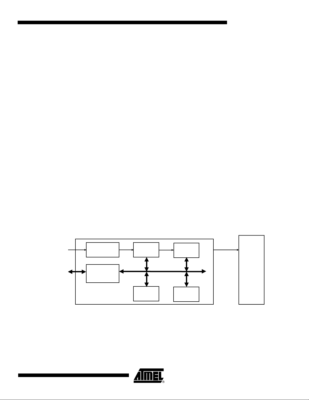
13. RTC: Real-time Clock
The AT91M55800A features a Real-time Clock (RTC) peripheral that is designed for very low
power consumption. It combines a complete time-of-day clock with alarm and a two-hundred
year Gregorian calendar, complemented by a programmable periodic interrupt.
The time and calendar values are coded in Binary-Coded Decimal (BCD) format. The time format can be 24-hour mode or 12-hour mode with an AM/PM indicator.
Updating time and calendar fields and configuring the alarm fields is performed by a parallel
capture on the 32-bit data bus. An entry control is performed to avoid loading registers with
incompatible BCD format data or with an incompatible date according to the current month/
year/century.
13.1 Year 2000 Conformity
The Real-time Clock complies fully with the Year 2000 Conformity Requirements as stated in
the British Standards Institution Document Ref BSI-DISC PD2000-1: “Year 2000 conformity
shall mean that neither performance nor functionality is affected by dates prior to, during and
after the year 2000”.
It has been tested to be compliant with the four associated rules:
1. No value for current date will cause any interruption in operation.
2. Date-based functionality must behave consistently for dates prior to, during and after
year 2000.
3. In all interfaces and data storage, the century in any date must be specified either
explicitly or by unambiguous algorithms or inferencing rules.
4. Year 2000 must be recognized as a leap year.
The RTC represents the year as a four-digit number (1998, 1999, 2000, 2001, etc.) so that the
century is unambiguously identified, in accordance with Rule 3.
AT91M55800A
Figure 13-1. RTC Block Diagram
SLCK:
Slow Clock
Advanced
Peripheral
Bus
32768 Divider
Bus Interface
Time
Entry
Control
Date
Interrupt
Control
RTCIRQ
AIC
1745D–ATARM–04-Nov-05
73
Page 74

13.2 Functional Description
The RTC provides a full Binary-Coded Decimal (BCD) clock which includes century (19/20),
year (with leap years), month, date, day, hours, minutes and seconds.
The valid year range is 1900 to 2099, a two-hundred year Gregorian calendar achieving full
Y2K compliance.
The RTC can operate in 24-hour mode or in 12-hour mode with an AM/PM indicator.
Corrections for leap years are included (all years divisible by 4 being leap years, including
year 2000). This is correct up to the year 2099.
13.2.1 Timing
The RTC is updated in real-time at one second intervals in normal mode for the counters of
seconds, at 1 minute intervals for the counter of minutes and so on.
Due to the asynchronous operation of the RTC with respect to the rest of the chip, to be certain that the value read in the RTC registers (century, year, month, date, day, hours, minutes,
seconds) are valid and stable, it is necessary to read these registers twice. If the data is the
same both times, then it is valid. Therefore, a minimum of two and a maximum of three
accesses is required.
13.2.2 Alarm
The RTC has five programmable fields with which to program an alarm: MONTH and DATE in
the Calendar Alarm Register (RTC_CAR), and SEC, MIN and HOUR in the Time Alarm Register (RTC_TAR). Each of these fields can be enabled or disabled using the bits MTHEN,
DATEN, SECEN, MINEN, HOUREN to match the alarm condition.
13.2.3 Error Checking
• If all the fields are enabled, an alarm flag is generated (the corresponding flag is asserted
and an interrupt generated if enabled) at a given month, date, hour, minute and second.
• If only the “seconds” field is enabled, then an alarm is generated every minute.
• Depending on the combination of fields enabled, a large number of possibilities are
available to the user ranging from minutes to 365/366 days.
A verification on user interface data is performed when accessing the century, year, month,
date, day, hours, minutes, seconds and alarms. A check is performed on illegal BCD entries
such as illegal date of the month with regards to the year and century configured.
If one of the time fields is not correct, the data is not loaded into the register/counter and a flag
is set in the Valid Entry Register (RTC_VER). This flag cannot be reset by the user. It is reset
as soon as an acceptable value is programmed. This avoids any further side effects in the
hardware. The same processing is done for the alarm.
The following checks are processed:
1. Century (check if it is in range 19 - 20)
2. Year (BCD entry check)
3. Date (check range 01 - 31)
4. Month (check if it is in BCD range 01 - 12,
check validity regarding “date”)
5. Day (check range 1 - 7)
74
AT91M55800A
1745D–ATARM–04-Nov-05
Page 75

6. Hour (BCD check, in 24-hour mode check range 00 - 23 and check that AM/PM flag is
not set if RTC is set in 24-Hour mode, in 12-Hour mode check range 01 - 12)
7. Minute (check BCD and range 00 - 59)
8. Second (check BCD and range 00 - 59)
Note: If the 12-hour mode is selected by means of the RTC_MODE register, a 12-hour value can be
13.2.4 Updating Time/Calendar
To update any of the time/calendar fields, the user must first stop the RTC by setting the corresponding field in the Mode Register (RTC_MR). Bit UPDTIM must be set to update time fields
(hour, minute, second) and bit UPDCAL must be set to update calendar fields (century, year,
month, date, day).
Then the user must poll or wait for the interrupt (if enabled) of bit ACKUPD in the Status Register (RTC_SR). Once the bit reads 1 (the user must clear this status bit by writing ACKUPD to
1 in RTC_SCR), the user can write to the appropriate register.
Once the update is finished, the user must reset (0) UPDTIM and/or UPDCAL in the Mode
Register (RTC_MR).
AT91M55800A
programmed and the returned value on RTC_TIME will be the corresponding 24-hour value.
The entry control checks the value of the AM/PM indicator (bit 22 of RTC_TIME register) to
determine the range to be checked.
When programming the calendar fields, the time fields remain enabled. This avoids a time slip
in case the user stays in the calendar update phase for several tens of seconds or more.
1745D–ATARM–04-Nov-05
75
Page 76

13.3 RTC User Interface
Base Address:0xFFFB8000 (Code Label RTC_BASE)
Table 13-1. RTC Memory Map
Offset Register Name Access Reset State
0x0000 Mode Register RTC_MR Read/Write 0x00000000
0x0004 Hour Mode Register RTC_HMR Read/Write 0x00000000
0x0008 Time Register RTC_TIMR Read/Write 0x00000000
0x000C Calendar Register RTC_CALR Read/Write 0x01819819
0x0010 Time Alarm Register RTC_TAR Read/Write 0x00000000
0x0014 Calendar Alarm Register RTC_CAR Read/Write 0x00000000
0x0018 Status Register RTC_SR Read-only 0x00000000
0x001C Status Clear Register RTC_SCR Write-only –
0x0020 Interrupt Enable Register RTC_IER Write-only –
0x0024 Interrupt Disable Register RTC_IDR Write-only –
0x0028 Interrupt Mask Register RTC_IMR Read-only 0x00000000
0x002C Valid Entry Register RTC_VER Read-only 0x00000000
76
AT91M55800A
1745D–ATARM–04-Nov-05
Page 77

AT91M55800A
13.3.1 RTC Mode Register Register Name:RTC_MR Access: Read/Write Offset: 0x00
31 30 29 28 27 26 25 24
––––––––
23 22 21 20 19 18 17 16
––––––
15 14 13 12 11 10 9 8
––––––
76543210
––––––
UPDCAL UPDTIM
• UPDTIM: Update Request Time Register (Code Label RTC_UPDTIM)
0 = Enables the RTC time counting.
1 = Stops the RTC time counting.
Time counting consists of second, minute and hour counters. Time counters can be programmed once this bit is set.
• UPDCAL: Update Request Calendar Register (Code Label RTC_UPDCAL)
0 = Disables the RTC calendar counting.
1 = Stops the RTC calendar counting.
Calendar counting consists of day, date, month, year and century counters. Calendar counters can be programmed once
this bit is set.
• TEVSEL: Time Event Selection
The event which generates the flag TIMEV in RTC_SR (Status Register) depends on the value of TEVSEL.
CEVSEL
TEVSEL
TEVSEL Event Code Label
0 0 Minute change RTC_TEVSEL_MN_CHG
0 1 Hour change RTC_TEVSEL_HR_CHG
1 0 Every day at midnight RTC_TEVSEL_EVDAY_MD
1 1 Every day at noon RTC_TEVSEL_EVDAY_NOON
• CEVSEL: Calendar Event Selection
The event which generates the flag CALEV in RTC_SR depends on the value of CEVSEL.
CEVSEL Event Code Label
0 0 Week change
0 1 Month change
1 0 Year change
1 1 Reserved –
(every Monday at time 00:00:00) RTC_CEVSEL_WEEK_CHG
(every 01 of each month at time 00:00:00) RTC_CEVSEL_MONTH_CHG
(every January 1st at time 00:00:00) RTC_CEVSEL_YEAR_CHG
1745D–ATARM–04-Nov-05
77
Page 78

13.3.2 RTC Hour Mode Register Register Name: RTC_HMR Access Type: Read/Write Reset State: 0x0 Offset: 0x04
31 30 29 28 27 26 25 24
––––––––
23 22 21 20 19 18 17 16
––––––––
15 14 13 12 11 10 9 8
––––––––
76543210
–––––––
• HRMOD: 12/24 Hour Mode
HRMOD Selected HRMOD Code Label
0 24-Hour mode is selected RTC_24_HRMOD
1 12-Hour mode is selected RTC_12_HRMOD
HRMOD
78
AT91M55800A
1745D–ATARM–04-Nov-05
Page 79

AT91M55800A
13.3.3 RTC Time Register Register Name: RTC_TIMR Access Type: Read/Write Reset State: 0x0 Offset: 0x08
31 30 29 28 27 26 25 24
––––––––
23 22 21 20 19 18 17 16
–
15 14 13 12 11 10 9 8
–
76543210
–
• SEC: Current Second (Code Label RTC_SEC)
The range that can be set is 0 - 59 (BCD).
The lowest four bits encode the units. The higher bits encode the tens.
• MIN: Current Minute (Code Label RTC_MIN)
The range that can be set is 0-59 (BCD).
The lowest four bits encode the units. The higher bits encode the tens.
• HOUR: Current Hour (Code Label RTC_HOUR)
The range that can be set is 1 - 12 (BCD) in 12-hour mode or 0 - 23 (BCD) in 24-hour mode.
• AMPM: Ante Meridiem Post Meridiem Indicator (Code Label RTC_AMPM)
This bit is the AM/PM indicator in 12-hour mode. It must be written at 0 if HRMOD in RTC_HMR defines 24-Hour mode.
0 = AM.
1 = PM.
AMPM HOUR
MIN
SEC
1745D–ATARM–04-Nov-05
79
Page 80

13.3.4 RTC Calendar Register Register Name: RTC_CALR Access Type: Read/Write Reset State: 0x01819819 Offset: 0x0C
31 30 29 28 27 26 25 24
––
23 22 21 20 19 18 17 16
DAY MONTH
15 14 13 12 11 10 9 8
YEAR
76543210
––
DATE
CENT
• CENT: Current Century (Code Label RTC_CENT)
The range that can be set is 19 - 20 (BCD).
The lowest four bits encode the units. The higher bits encode the tens.
• YEAR: Current Year (Code Label RTC_YEAR)
The range that can be set is 00 - 99 (BCD).
The lowest four bits encode the units. The higher bits encode the tens.
• MONTH: Current Month (Code Label RTC_MONTH)
The range that can be set is 01 - 12 (BCD).
The lowest four bits encode the units. The higher bits encode the tens.
• DAY: Current Day (Code Label RTC_DAY)
The range that can be set is 1 - 7 (BCD).
The significance of the number (which number represents which day) is user defined as it has no effect on the date
counter.
• DATE: Current Date (Code Label RTC_DATE)
The range that can be set is 01 - 31 (BCD).
The lowest four bits encode the units. The higher bits encode the tens.
80
AT91M55800A
1745D–ATARM–04-Nov-05
Page 81

AT91M55800A
13.3.5 RTC Time Alarm Register Register Name: RTC_TAR Access Type: Read/Write Reset State: 0x0 Offset: 0x10
31 30 29 28 27 26 25 24
––––––––
23 22 21 20 19 18 17 16
HOUREN AMPM HOUR
15 14 13 12 11 10 9 8
MINEN MIN
76543210
SECEN SEC
• SEC: Second Alarm
This field is the alarm field corresponding to the BCD-coded second counter.
• SECEN: Second Alarm Enable
SECEN Selected SECEN Code Label
0 The second matching alarm is disabled. RTC_SEC_ALARM_DIS
1 The second matching alarm is enabled. RTC_SEC_ALARM_EN
• MIN: Minute Alarm
This field is the alarm field corresponding to the BCD-coded minute counter.
• MINEN: Minute Alarm Enable
MINEN Selected MINEN Code Label
0 The minute matching alarm is disabled. RTC_MIN_ALARM_DIS
1 The minute matching alarm is enabled. RTC_MIN_ALARM_EN
• HOUR: Hour Alarm
This field is the alarm field corresponding to the BCD-coded hour counter.
• AMPM: AM/PM Indicator
This bit is the AM/PM indicator in 12-Hour mode. It must be written at 0 if HRMOD in RTC_HMR defines 24-Hour mode.
• HOUREN: Hour Alarm Enable
HOUREN Selected HOUREN Code Label
0 The hour matching alarm is disabled. RTC_HOUR_ALARM_DIS
1 The hour matching alarm is enabled. RTC_HOUR_ALARM_EN
1745D–ATARM–04-Nov-05
81
Page 82

13.3.6 RTC Calendar Alarm Register Register Name: RTC_CAR Access Type: Read/Write Reset State: 0x0 Offset: 0x14
31 30 29 28 27 26 25 24
DATEN
23 22 21 20 19 18 17 16
MTHEN
15 14 13 12 11 10 9 8
––––––––
76543210
––––––––
–
––
DATE
MONTH
• MONTH: Month Alarm
This field is the alarm field corresponding to the BCD-coded month counter.
• MTHEN: Month Alarm Enable
MTHEN Selected MTHEN Code Label
0 The month matching alarm is disabled. RTC_MONTH_ALARM_DIS
1 The month matching alarm is enabled. RTC_MONTH_ALARM_EN
•DATE: Date Alarm
This field is the alarm field corresponding to the BCD-coded date counter.
• DATEN: Date Alarm Enable
DATEN Selected DATEN Code Label
0 The date matching alarm is disabled. RTC_DATE_ALARM_DIS
1 The date matching alarm is enabled. RTC_DATE_ALARM_EN
82
AT91M55800A
1745D–ATARM–04-Nov-05
Page 83

AT91M55800A
13.3.7 RTC Status Register Register Name: RTC_SR Access Type: Read-only Reset State: 0x0 Offset: 0x18
31 30 29 28 27 26 25 24
––––––––
23 22 21 20 19 18 17 16
––––––––
15 14 13 12 11 10 9 8
––––––––
76543210
–––
• ACKUPD: Acknowledge for Update (Code Label RTC_ACKUPD)
0 = Time and Calendar registers cannot be updated.
1 = Time and Calendar registers can be updated.
• ALARM: Alarm Flag (Code Label RTC_ALARM)
0 = No alarm matching condition occurred.
1 = An alarm matching condition has occurred.
• SEC: Second Event (Code Label RTC_SEC)
0 = No second event has occurred since the last clear.
1 = At least one second event has occurred since the last clear.
• TIMEV: Time Event (Code Label RTC_TIMEV)
0 = No time event has occurred since the last clear.
1 = At least one time event has occurred since the last clear.
The time event is selected in the TEVSEV field in RTC_CR and can be any one of the following events: minute change,
hour change, noon, midnight (day change).
• CALEV: Calendar Event (Code Label RTC_CALEV)
0 = No calendar event has occurred since the last clear.
1 = At least one calendar event has occurred since the last clear.
The calendar event is selected in the CEVSEL field in RTC_CR and can be any one of the following events: week change,
month change, year change.
CALEV TIMEV SEC ALARM ACKUPD
1745D–ATARM–04-Nov-05
83
Page 84

13.3.8 RTC Status Clear Register Register Name: RTC_SCR Access Type: Write-only Offset: 0x1C
31 30 29 28 27 26 25 24
––––––––
23 22 21 20 19 18 17 16
––––––––
15 14 13 12 11 10 9 8
––––––––
76543210
–––
CALEV TIMEV SEC ALARM ACKUPD
• ACKUPD: Acknowledge for Update Interrupt Clear (Code Label RTC_ACKUPD)
0 = No effect.
1 = Clears Acknowledge for Update status bit.
• ALARM: Alarm Flag Interrupt Clear (Code Label RTC_ALARM)
0 = No effect.
1 = Clears Alarm Flag bit.
• SEC: Second Event Interrupt Clear (Code Label RTC_SEC)
0 = No effect.
1 = Clears Second Event bit.
• TIMEV: Time Event Interrupt Clear (Code Label RTC_TIMEV)
0 = No effect.
1 = Clears Time Event bit.
• CALEV: Calendar Event Interrupt Clear (Code Label RTC_CALEV)
0 = No effect.
1 = Clears Calendar Event bit.
84
AT91M55800A
1745D–ATARM–04-Nov-05
Page 85

AT91M55800A
13.3.9 RTC Interrupt Enable Register Register Name: RTC_IER Access Type: Write-only Offset: 0x20
31 30 29 28 27 26 25 24
––––––––
23 22 21 20 19 18 17 16
––––––––
15 14 13 12 11 10 9 8
––––––––
76543210
–––
• ACKUPD: Acknowledge Update Interrupt Enable (Code Label RTC_ACKUPD)
0 = No effect.
1 = The acknowledge for update interrupt is enabled.
• ALARM: Alarm Interrupt Enable (Code Label RTC_ALARM)
0 = No effect.
1 = The alarm interrupt is enabled.
• SEC: Second Event Interrupt Enable (Code Label RTC_SEC)
0 = No effect.
1 = The second periodic interrupt is enabled.
• TIMEV: Time Event Interrupt Enable (Code Label RTC_TIMEV)
0 = No effect.
1 = The selected time event interrupt is enabled.
• CALEV: Calendar Event Interrupt Enable (Code Label RTC_CALEV)
0 = No effect.
1 = The selected calendar event interrupt is enabled.
CALEV TIMEV SEC ALARM ACKUPD
1745D–ATARM–04-Nov-05
85
Page 86

13.3.10 RTC Interrupt Disable Register Register Name: RTC_IDR Access Type: Write-only Offset: 0x24
31 30 29 28 27 26 25 24
––––––––
23 22 21 20 19 18 17 16
––––––––
15 14 13 12 11 10 9 8
––––––––
76543210
–––
CALEV TIMEV SEC ALARM ACKUPD
• ACKUPD: Acknowledge Update Interrupt Disable (Code Label RTC_ACKUPD)
0 = No effect.
1 = The acknowledge for update interrupt is disabled.
• ALARM: Alarm Interrupt Disable (Code Label RTC_ALARM)
0 = No effect.
1 = The alarm interrupt is disabled.
• SEC: Second Event Interrupt Disable (Code Label RTC_SEC)
0 = No effect.
1 = The second periodic interrupt is disabled.
• TIMEV: Time Event Interrupt Disable (Code Label RTC_TIMEV)
0 = No effect.
1 = The selected time event interrupt is disabled.
• CALEV: Calendar Event Interrupt Disable (Code Label RTC_CALEV)
0 = No effect.
1 = The selected calendar event interrupt is disabled.
86
AT91M55800A
1745D–ATARM–04-Nov-05
Page 87

AT91M55800A
13.3.11 RTC Interrupt Mask Register Register Name: RTC_IMR Access Type: Read-only Reset State: 0x0 Offset: 0x28
31 30 29 28 27 26 25 24
––––––––
23 22 21 20 19 18 17 16
––––––––
15 14 13 12 11 10 9 8
––––––––
76543210
–––
• ACKUPD: Acknowledge Update Interrupt Mask (Code Label RTC_ACKUPD)
0 = The acknowledge for update interrupt is disabled.
1 = The acknowledge for update interrupt is enabled.
• ALARM: Alarm Interrupt Mask (Code Label RTC_ALARM)
0 = The alarm interrupt is disabled.
1 = The alarm interrupt is enabled.
• SEC: Second Event Interrupt Mask (Code Label RTC_SEC)
0 = The second periodic interrupt is disabled.
1 = The second periodic interrupt is enabled.
• TIMEV: Time Event Interrupt Mask (Code Label RTC_TIMEV)
0 = The selected time event interrupt is disabled.
1 = The selected time event interrupt is enabled.
• CALEV: Calendar Event Interrupt Mask (Code Label RTC_CALEV)
0 = The selected calendar event interrupt is disabled.
1 = The selected calendar event interrupt is enabled.
CALEV TIMEV SEC ALARM ACKUPD
1745D–ATARM–04-Nov-05
87
Page 88

13.3.12 RTC Valid Entry Register Register Name: RTC_VER Access Type: Read-only Reset State: 0x0 Offset: 0x2C
31 30 29 28 27 26 25 24
––––––––
23 22 21 20 19 18 17 16
––––––––
15 14 13 12 11 10 9 8
––––––––
76543210
––––
NVCAL NVTAL NVC NVT
• NVT: Non-Valid Time (Code Label RTC_NVT)
0 = No invalid data has been detected in RTC_TIMR.
1 = RTC_TIMR has contained invalid data since it was last programmed.
• NVC: Non-Valid Calendar (Code Label RTC_NVC)
0 = No invalid data has been detected in RTC_CALR.
1 = RTC_CALR has contained invalid data since it was last programmed.
• NVTAL: Non-Valid Time Alarm (Code Label RTC_NVTAL)
0 = No invalid data has been detected in RTC_TAR.
1 = RTC_TAR has contained invalid data since it was last programmed.
• NVCAL: Non-Valid Calendar Alarm (Code Label RTC_NVCAL)
0 = No invalid data has been detected in RTC_CAR.
1 = RTC_CAR has contained invalid data since it was last programmed.
88
AT91M55800A
1745D–ATARM–04-Nov-05
Page 89
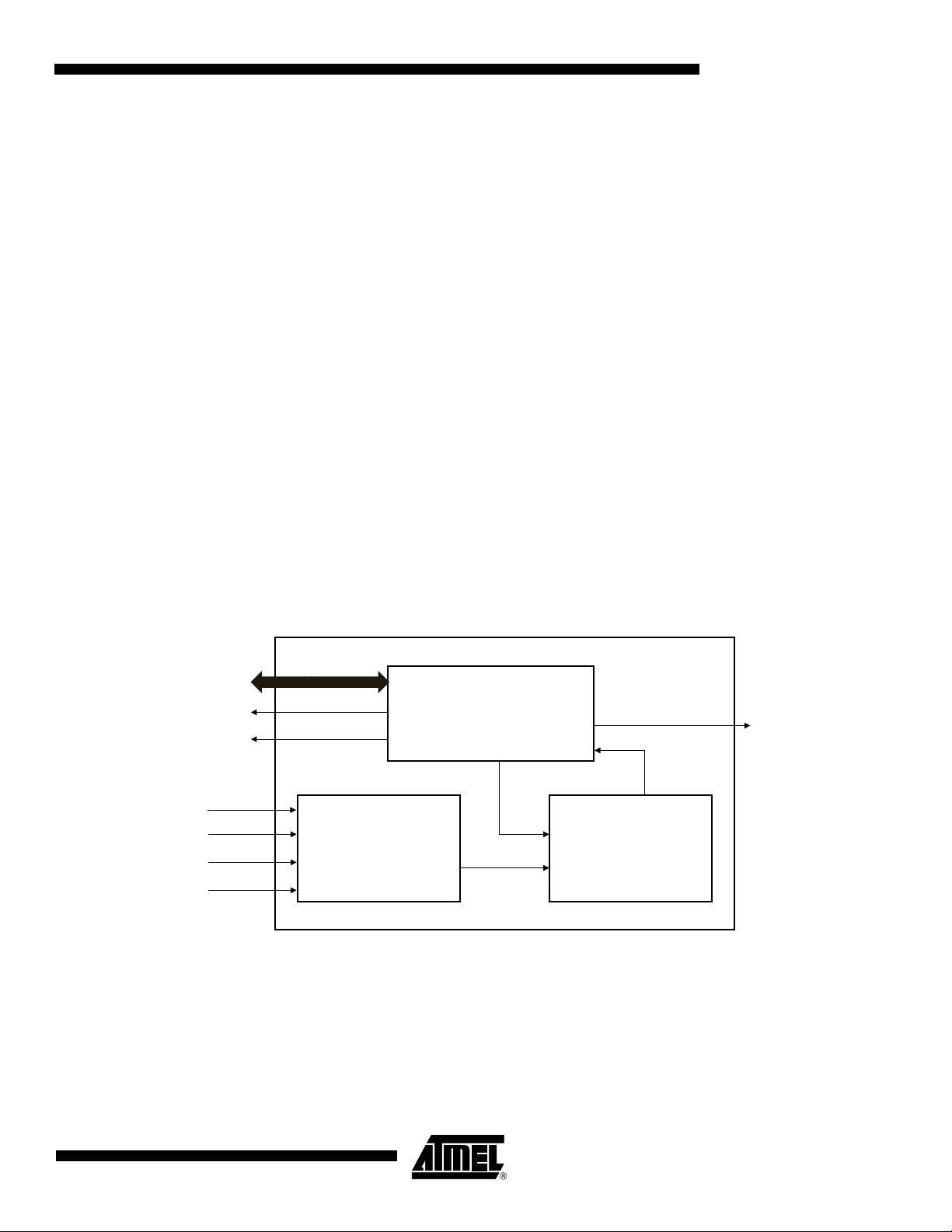
14. WD: Watchdog Timer
The AT91M55800A has an internal Watchdog Timer that can be used to prevent system lockup if the software becomes trapped in a deadlock.
In normal operation the user reloads the watchdog at regular intervals before the timer overflow occurs. If an overflow does occur, the watchdog timer generates one or a combination of
the following signals, depending on the parameters in WD_OMR (Overflow Mode Register):
• If RSTEN is set, an internal reset is generated (WD_RESET as shown in Figure 14-1).
• If IRQEN is set, a pulse is generated on the signal WDIRQ which is connected to the
Advanced Interrupt Controller
• If EXTEN is set, a low level is driven on the NWDOVF signal for a duration of 8 MCK cycles.
The watchdog timer has a 16-bit down counter. Bits 12 - 15 of the value loaded when the
watchdog is restarted are programmable using the HPVC parameter in WD_CMR (Clock
Mode). Four clock sources are available to the watchdog counter: MCK/32, MCK/128,
MCK/1024 or MCK/4096. The selection is made using the WDCLKS parameter in WD_CMR.
This provides a programmable time-out period of 4 ms to 8 sec. with a 33 MHz system clock.
All write accesses are protected by control access keys to help prevent corruption of the
watchdog should an error condition occur. To update the contents of the mode and control
registers it is necessary to write the correct bit pattern to the control access key bits at the
same time as the control bits are written (the same write access).
AT91M55800A
Figure 14-1. Watchdog Timer Block Diagram
Advanced
Peripheral
Bus (APB)
WD_RESET
WDIRQ
MCK/32
MCK/128
MCK/1024
MCK/4096
Clock Select
Control Logic
CLK_CNT
Clear
NWDOVF
Overflow
16-Bit
Programmable
Down Counter
1745D–ATARM–04-Nov-05
89
Page 90

14.0.1 WD User Interface WD Base Address: 0xFFFF8000 (Code Label WD_BASE)
Table 14-1. WD Memory Map
Offset Register Name Access Reset State
0x00 Overflow Mode Register WD_OMR Read/Write 0
0x04 Clock Mode Register WD_CMR Read/Write 0
0x08 Control Register WD_CR Write-only –
0x0C Status Register WD_SR Read-only 0
90
AT91M55800A
1745D–ATARM–04-Nov-05
Page 91

AT91M55800A
14.0.2 WD Overflow Mode Register Name: WD_OMR Access: Read/Write Reset Value: 0 Offset: 0x00
31 30 29 28 27 26 25 24
––––––––
23 22 21 20 19 18 17 16
––––––––
15 14 13 12 11 10 9 8
OKEY
76543210
OKEY EXTEN IRQEN RSTEN WDEN
• WDEN: Watchdog Enable (Code Label WD_WDEN)
0 = Watchdog is disabled and does not generate any signals.
1 = Watchdog is enabled and generates enabled signals.
• RSTEN: Reset Enable (Code Label WD_RSTEN)
0 = Generation of an internal reset by the Watchdog is disabled.
1 = When overflow occurs, the Watchdog generates an internal reset.
• IRQEN: Interrupt Enable (Code Label WD_IRQEN)
0 = Generation of an interrupt by the Watchdog is disabled.
1 = When overflow occurs, the Watchdog generates an interrupt.
• EXTEN: External Signal Enable (Code Label WD_EXTEN)
0 = Generation of a pulse on the pin NWDOVF by the Watchdog is disabled.
1 = When an overflow occurs, a pulse on the pin NWDOVF is generated.
• OKEY: Overflow Access Key (Code Label WD_OKEY)
Used only when writing WD_OMR. OKEY is read as 0.
0x234 = Write access in WD_OMR is allowed.
Other value = Write access in WD_OMR is prohibited.
1745D–ATARM–04-Nov-05
91
Page 92

14.0.3 WD Clock Mode Register Name: WD_CMR Access: Read/Write Reset Value: 0 Offset: 0x04
31 30 29 28 27 26 25 24
––––––––
23 22 21 20 19 18 17 16
––––––––
15 14 13 12 11 10 9 8
CKEY
76543210
CKEY
–
HPCV WDCLKS
• WDCLKS: Clock Selection
Code Label
WDCLKS Clock Selected
0 0 MCK/32 WD_WDCLKS_MCK32
0 1 MCK/128 WD_WDCLKS_MCK128
1 0 MCK/1024 WD_WDCLKS_MCK1024
1 1 MCK/4096 WD_WDCLKS_MCK4096
WD_WDCLKS
• HPCV: High Pre-load Counter Value (Code Label WD_HPCV)
Counter is preloaded when watchdog counter is restarted with bits 0 to 11 set (FFF) and bits 12 to 15 equaling HPCV.
• CKEY: Clock Access Key (Code Label WD_CKEY)
Used only when writing WD_CMR. CKEY is read as 0.
0x06E: Write access in WD_CMR is allowed.
Other value: Write access in WD_CMR is prohibited.
92
AT91M55800A
1745D–ATARM–04-Nov-05
Page 93

AT91M55800A
14.0.4 WD Control Register Name: WD_CR Access: Write-only Offset: 0x08
31 30 29 28 27 26 25 24
––––––––
23 22 21 20 19 18 17 16
––––––––
15 14 13 12 11 10 9 8
RSTKEY
76543210
RSTKEY
• RSTKEY: Restart Key (Code Label WD_RSTKEY)
0xC071 = Watch Dog counter is restarted.
Other value = No effect.
1745D–ATARM–04-Nov-05
93
Page 94

14.0.5 WD Status Register Name: WD_SR Access: Read-only Reset Value: 0x0 Offset: 0x0C
31 30 29 28 27 26 25 24
––––––––
23 22 21 20 19 18 17 16
––––––––
15 14 13 12 11 10 9 8
––––––––
76543210
–––––––
WDOVF
• WDOVF: Watchdog Overflow (Code Label WD_WDOVF)
0 = No watchdog overflow.
1 = A watchdog overflow has occurred since the last restart of the watchdog counter or since internal or external reset.
14.0.6 WD Enabling Sequence
To enable the Watchdog Timer, the sequence is as follows:
1. Disable the Watchdog by clearing the bit WDEN:
Write 0x2340 to WD_OMR
This step is unnecessary if the WD is already disabled (reset state).
2. Initialize the WD Clock Mode Register:
3. Write 0x373C to WD_CMR
(HPCV = 15 and WDCLKS = MCK/8)
4. Restart the timer: Write 0xC071 to WD_CR
5. Enable the watchdog:
Write 0x2345 to WD_OMR (interrupt enabled)
94
AT91M55800A
1745D–ATARM–04-Nov-05
Page 95

15. AIC: Advanced Interrupt Controller
The AT91M55800A has an 8-level priority, individually maskable, vectored interrupt controller.
This feature substantially reduces the software and real-time overhead in handling internal
and external interrupts.
The interrupt controller is connected to the NFIQ (fast interrupt request) and the NIRQ (standard interrupt request) inputs of the ARM7TDMI processor. The processor’s NFIQ line can
only be asserted by the external fast interrupt request input: FIQ. The NIRQ line can be
asserted by the interrupts generated by the on-chip peripherals and the external interrupt
request lines: IRQ0 to IRQ5.
An 8-level priority encoder allows the customer to define the priority between the different
NIRQ interrupt sources.
Internal sources are programmed to be level sensitive or edge-triggered. External sources can
be programmed to be positive or negative edge-triggered or high- or low-level sensitive.
The interrupt sources are listed in Table 15-1 on page 96 and the AIC programmable registers
in Table 15-2 on page 101.
Figure 15-1. Advanced Interrupt Controller Block Diagram
AT91M55800A
FIQ Source
Advanced Peripheral
Bus (APB)
Internal Interrupt Sources
External Interrupt Sources
Note: After a hardware reset, the AIC pins are controlled by the PIO Controller. They must be configured to be controlled by the
peripheral before being used.
Memorization
Control
Logic
Memorization
Prioritization
Controller
NFIQ
Manager
NIRQ
Manager
NFIQ
ARM7TDMI
Core
NIRQ
1745D–ATARM–04-Nov-05
95
Page 96

Table 15-1. AIC Interrupt Sources
Interrupt Source Interrupt Name Interrupt Description
0 FIQ Fast interrupt
1 SWIRQ Software interrupt
2 US0IRQ USART Channel 0 interrupt
3 US1IRQ USART Channel 1 interrupt
4 US2IRQ USART Channel 2 interrupt
5 SPIRQ SPI interrupt
6 TC0IRQ Timer Channel 0 interrupt
7 TC1IRQ Timer Channel 1 interrupt
8 TC2IRQ Timer Channel 2 interrupt
9 TC3IRQ Timer Channel 3 interrupt
10 TC4IRQ Timer Channel 4 interrupt
11 TC5IRQ Timer Channel 5 interrupt
12 WDIRQ Watchdog interrupt
13 PIOAIRQ Parallel I/O Controller A interrupt
14 PIOBIRQ Parallel I/O Controller B interrupt
15 AD0IRQ Analog-to-digital Converter Channel 0 interrupt
16 AD1IRQ Analog-to-digital Converter Channel 1 interrupt
17 DA0IRQ Digital-to-analog Converter Channel 0 interrupt
18 DA1IRQ Digital-to-analog Converter Channel 1 interrupt
19 RTCIRQ Real-time Clock interrupt
20 APMCIRQ Advanced Power Management Controller interrupt
21 – Reserved
22 – Reserved
23 SLCKIRQ Slow Clock Interrupt
24 IRQ5 External interrupt 5
25 IRQ4 External interrupt 4
26 IRQ3 External interrupt 3
27 IRQ2 External interrupt 2
28 IRQ1 External interrupt 1
29 IRQ0 External interrupt 0
30 COMMRX RX Debug Communication Channel interrupt
31 COMMTX TX Debug Communication Channel interrupt
96
AT91M55800A
1745D–ATARM–04-Nov-05
Page 97

15.1 Hardware Interrupt Vectoring
The hardware interrupt vectoring reduces the number of instructions to reach the interrupt
handler to only one. By storing the following instruction at address 0x00000018, the processor
loads the program counter with the interrupt handler address stored in the AIC_IVR register.
Execution is then vectored to the interrupt handler corresponding to the current interrupt.
ldr PC,[PC,# -&F20]
The current interrupt is the interrupt with the highest priority when the Interrupt Vector Register
(AIC_IVR) is read. The value read in the AIC_IVR corresponds to the address stored in the
Source Vector Register (AIC_SVR) of the current interrupt. Each interrupt source has its corresponding AIC_SVR. In order to take advantage of the hardware interrupt vectoring it is
necessary to store the address of each interrupt handler in the corresponding AIC_SVR, at
system initialization.
15.2 Priority Controller
The NIRQ line is controlled by an 8-level priority encoder. Each source has a programmable
priority level of 7 to 0. Level 7 is the highest priority and level 0 the lowest.
When the AIC receives more than one unmasked interrupt at a time, the interrupt with the
highest priority is serviced first. If both interrupts have equal priority, the interrupt with the lowest interrupt source number (see Table Table 15-1) is serviced first.
AT91M55800A
The current priority level is defined as the priority level of the current interrupt at the time the
register AIC_IVR is read (the interrupt which is serviced).
In the case when a higher priority unmasked interrupt occurs while an interrupt already exists,
there are two possible outcomes depending on whether the AIC_IVR has been read.
When the end of interrupt command register (AIC_EOICR) is written the current interrupt level
is updated with the last stored interrupt level from the stack (if any). Hence at the end of a
higher priority interrupt, the AIC returns to the previous state corresponding to the preceding
lower priority interrupt which had been interrupted.
15.3 Interrupt Handling
The interrupt handler must read the AIC_IVR as soon as possible. This de-asserts the NIRQ
request to the processor and clears the interrupt in case it is programmed to be edge-triggered. This permits the AIC to assert the NIRQ line again when a higher priority unmasked
interrupt occurs.
• If the NIRQ line has been asserted but the AIC_IVR has not been read, then the processor
reads the new higher priority interrupt handler address in the AIC_IVR register and the
current interrupt level is updated.
• If the processor has already read the AIC_IVR then the NIRQ line is reasserted. When the
processor has authorized nested interrupts to occur and reads the AIC_IVR again, it reads
the new, higher priority interrupt handler address. At the same time the current priority
value is pushed onto a first-in last-out stack and the current priority is updated to the higher
priority.
1745D–ATARM–04-Nov-05
At the end of the interrupt service routine, the end of interrupt command register (AIC_EOICR)
must be written. This allows pending interrupts to be serviced.
97
Page 98

15.4 Interrupt Masking
Each interrupt source, including FIQ, can be enabled or disabled using the command registers
AIC_IECR and AIC_IDCR. The interrupt mask can be read in the Read-only register AIC_IMR.
A disabled interrupt does not affect the servicing of other interrupts.
15.5 Interrupt Clearing and Setting
All interrupt sources which are programmed to be edge-triggered (including FIQ) can be individually set or cleared by respectively writing to the registers AIC_ISCR and AIC_ICCR. This
function of the interrupt controller is available for auto-test or software debug purposes.
15.6 Fast Interrupt Request
The external FIQ line is the only source which can raise a fast interrupt request to the processor. Therefore, it has no priority controller.
The external FIQ line can be programmed to be positive or negative edge-triggered or high- or
low-level sensitive in the AIC_SMR0 register.
The fast interrupt handler address can be stored in the AIC_SVR0 register. The value written
into this register is available by reading the AIC_FVR register when an FIQ interrupt is raised.
By storing the following instruction at address 0x0000001C, the processor loads the program
counter with the interrupt handler address stored in the AIC_FVR register.
ldr PC,[PC,# -&F20]
Alternatively, the interrupt handler can be stored starting from address 0x0000001C as
described in the ARM7TDMI datasheet.
15.7 Software Interrupt
Interrupt source 1 of the advanced interrupt controller is a software interrupt. It must be programmed to be edge-triggered in order to set or clear it by writing to the AIC_ISCR and
AIC_ICCR.
This is totally independent of the SWI instruction of the ARM7TDMI processor.
15.8 Spurious Interrupt
When the AIC asserts the NIRQ line, the ARM7TDMI enters IRQ mode and the interrupt handler reads the IVR. It may happen that the AIC de-asserts the NIRQ line after the core has
taken into account the NIRQ assertion and before the read of the IVR.
This behavior is called a Spurious Interrupt.
The AIC is able to detect these Spurious Interrupts and returns the Spurious Vector when the
IVR is read. The Spurious Vector can be programmed by the user when the vector table is
initialized.
A Spurious Interrupt may occur in the following cases:
• With any sources programmed to be level sensitive, if the interrupt signal of the AIC input is
de-asserted at the same time as it is taken into account by the ARM7TDMI.
• If an interrupt is asserted at the same time as the software is disabling the corresponding
source through AIC_IDCR (this can happen due to the pipelining of the ARM Core).
98
AT91M55800A
1745D–ATARM–04-Nov-05
Page 99

15.9 Protect Mode
AT91M55800A
The same mechanism of Spurious Interrupt occurs if the ARM7TDMI reads the IVR (application software or ICE) when there is no interrupt pending. This mechanism is also valid for the
FIQ interrupts.
Once the AIC enters the Spurious Interrupt management, it asserts neither the NIRQ nor the
NFIQ lines to the ARM7TDMI as long as the Spurious Interrupt is not acknowledged. Therefore, it is mandatory for the Spurious Interrupt Service Routine to acknowledge the “Spurious”
behavior by writing to the AIC_EOICR (End of Interrupt) before returning to the interrupted
software. It also can perform other operation(s), e.g. trace possible undesirable behavior.
The Protect Mode permits reading of the Interrupt Vector Register without performing the
associated automatic operations. This is necessary when working with a debug system.
When a Debug Monitor or an ICE reads the AIC User Interface, the IVR could be read. This
would have the following consequences in normal mode:
• If an enabled interrupt with a higher priority than the current one is pending, it would be
stacked.
• If there is no enabled pending interrupt, the spurious vector would be returned.
In either case, an End of Interrupt Command would be necessary to acknowledge and to
restore the context of the AIC. This operation is generally not performed by the debug system.
Hence the debug system would become strongly intrusive, and could cause the application to
enter an undesired state.
This is avoided by using Protect Mode.
The Protect Mode is enabled by setting the AIC bit in the SF Protect Mode Register.
When Protect Mode is enabled, the AIC performs interrupt stacking only when a write access
is performed on the AIC_IVR. Therefore, the Interrupt Service Routines must write (arbitrary
data) to the AIC_IVR just after reading it.
The new context of the AIC, including the value of the Interrupt Status Register (AIC_ISR), is
updated with the current interrupt only when IVR is written.
An AIC_IVR read on its own (e.g. by a debugger), modifies neither the AIC context nor the
AIC_ISR.
Extra AIC_IVR reads performed in between the read and the write can cause unpredictable
results. Therefore, it is strongly recommended not to set a breakpoint between these 2
actions, nor to stop the software.
The debug system must not write to the AIC_IVR as this would cause undesirable effects.
1745D–ATARM–04-Nov-05
99
Page 100

The following table shows the main steps of an interrupt and the order in which they are performed according to the mode:
Action Normal Mode Protect Mode
Calculate active interrupt
(higher than current or spurious)
Determine and return the vector of the
active interrupt
Memorize interrupt Read AIC_IVR Read AIC_IVR
Push on internal stack the current priority
level
Acknowledge the interrupt
No effect
Notes: 1. NIRQ de-assertion and automatic interrupt clearing if the source is programmed as level
(2)
sensitive
2. Note that software which has been written and debugged using Protect Mode will run correctly in Normal Mode without modification. However in Normal Mode the AIC_IVR write has
no effect and can be removed to optimize the code.
(1)
Read AIC_IVR Read AIC_IVR
Read AIC_IVR Read AIC_IVR
Read AIC_IVR Write AIC_IVR
Read AIC_IVR Write AIC_IVR
Write AIC_IVR –
100
AT91M55800A
1745D–ATARM–04-Nov-05
 Loading...