


查询AT91M43300供应商
Features
• Utilizes the ARM7TDMI
– High-performance 32-bit RISC Architecture
– High-density 16-bit Instruction Set
– Leader in MIPS/Watt
– Embedded ICE (In-Circuit Emulation)
• 3K Bytes Internal RAM
• Fully-programmable External Bus Interface (EBI)
– Maximum External Address Space of 64M Bytes
– Up to 8 Chip Selects
– Software-programmable 8/16-bit External Data Bus
• 8-channel Peripheral Data Controller
• 8-level Priority, Individually-maskable, Vectored Interrupt Controller
– 5 External Interrupts, including a High-priority, Low-latency Interrupt Request
• 58 Programmable I/O Lines
• 6-channel 16-bit Timer/Counter
– 6 External Clock Inputs
– 2 Multi-purpose I/O Pins per Channel
• 3 USARTs
– 2 Dedicated Peripheral Data Controller (PDC) Channels per USART
– Support for up to 9-bit Data Transfers
• Master/Slave SPI Interface
– 2 Dedicated Peripheral Data Controller (PDC) Channels
– 8- to 16-bit Programmable Data Length
– 4 External Slave Chip Selects
• Programmable Watchdog Timer
• Power Management Controller (PMC)
– CPU and Peripherals can be Deactivated Individually
• IEEE 1149.1 JTAG Boundary Scan on all Active Pins
• Fully Static Operation: 0 Hz to 25 MHz (12 MHz @ 1.8V)
• 1.8V to 3.6V Core Operating Voltage Range
• 2.7V to 5.5V I/O Operating Voltage Range
• -40° to +85°C Operating Temperature Range
• Available in a 144-ball PBGA Package
™
ARM® Thumb® Processor Core
AT91
ARM
®
Thumb®
Microcontrollers
AT91M43300
Description
The AT91M43300 is a member of the Atmel AT91 16/32-bit Microcontroller family,
which is based on the ARM7TDMI processor core.
This processor has a high-performance 32-bit RISC architecture with a high-density
16-bit instruction set and features very low power consumption. In addition, a large
number of internally banked registers result in very fast exception handling, making
the device ideal for real-time control applications. The AT91 ARM-based MCU family
also features Atmel’s high-density, in-system programmable, nonvolatile memory
technology.
The AT91M43300 has a direct connection to off-chip memory, including Flash,
through the fully-programmable External Bus Interface.
The AT91M43300 is manufactured using Atmel’s high-density CMOS technology. By
combining the ARM7TDMI microcontroller core with an on-chip SRAM, and a wide
range of peripheral functions on a monolithic chip, the AT91M43300 provides a highlyflexible and cost-effective solution to many compute-intensive multi-processor applications.
The compact BGA package reduces required board space to an absolute minimum.
Rev. 1322A–10/99
1

Pin Description
Table 1. AT91M43300 Pin Description
Module Name Function Type
A0 - A23 Address Bus Output – All valid after reset
D0 - D15 Data Bus I/O –
CS4 - CS7 Chip Select Output High A23 - A20 after reset
NCS0 - NCS3 Chip Select Output Low
NWR0 Lower Byte 0 Write Signal Output Low Used in Byte Write option
NWR1 Lower Byte 1 Write Signal Output Low Used in Byte Write option
EBI
AIC
Timer
USART
SPI
PIO
WD NWDOVF Watchdog Timer Overflow Output Low Open drain
Clock
Reset NRST Hardware Reset Input Input Low Schmitt trigger, internal pull-up
JTAG/ICE
Power
Emulation NTRI Tristate Mode Enable Input Low Sampled during reset
NRD Read Signal Output Low Used in Byte Write option
NWE Write Enable Output Low Used in Byte Select option
NOE Output Enable Output Low Used in Byte Select option
NUB Upper Byte Select (16-bit SRAM) Output Low Used in Byte Select option
NLB Lower Byte Select (16-bit SRAM) Output Low Used in Byte Select option
NWAIT Wait Input Input Low
BMS Boot Mode Select Input – Sampled during reset
IRQ0 - IRQ3 External Interrupt Request Input – PIO-controlled after reset
FIQ Fast External Interrupt Request Input – PIO-controlled after reset
TCLK0 - TCLK5 Timer External Clock Input – PIO-controlled after reset
TIOA0 - TIOA5 Multi-purpose Timer I/O Pin A I/O – PIO-controlled after reset
TIOB0 - TIOB5 Multi-purpose Timer I/O Pin B I/O – PIO-controlled after reset
SCK0 - SCK2 External Serial Clock I/O – PIO-controlled after reset
TXD0 - TXD2 Transmit Data Output Output – PIO-controlled after reset
RXD0 - RXD2 Receive Data Input Input – PIO-controlled after reset
SPCK SPI Clock I/O – PIO-controlled after reset
MISO Master In Slave Out I/O – PIO-controlled after reset
MOSI Master Out Slave In I/O – PIO-controlled after reset
NSS Slave Select Input Low PIO-controlled after reset
NPCS0 - NPCS3 Peripheral Chip Select Output Low PIO-controlled after reset
PA0 - PA29 Programmable I/O Port A I/O – Input after reset
PB0 - PB27 Programmable I/O Port B I/O – Input after reset
MCKI Master Clock Input Input – Schmitt trigger
MCKO Master Clock Output Output –
JTAGSEL Selects between JTAG and ICE mode Input –
TMS Test Mode Select Input – Schmitt trigger, internal pull-up
TDI Test Data In Input – Schmitt trigger, internal pull-up
TDO Test Data Out Output –
TCK Test Clock Input – Schmitt trigger, internal pull-up
NTRST Test Reset Input Input Low Schmitt trigger, internal pull-up
VDDIO I/O Power Power – 3V or 5V nominal supply
VDDCORE Core Power Power – 2.0V or 3V nominal supply
GND Ground Ground –
Active
Level
Comments
High enables IEEE 1149.1 JTAG
boundary scan
2
AT91M43300
Pin Configuration
Figure 1. AT91M43300 in 144-ball BGA Package (top view)
123456789101112
AT91M43300
A
B
C
D
E
F
G
H
J
K
L
M
NUB
NOE
NWR1
NCS0 NWE
NCS2 NCS1 VDDCORE NCS3 GND NRST PB10 PB14 PB9 VDDCORE
A3 A2 GND PB13 PB16 PB12
VDDIO GND A10 PA7
A9 A14 A8 PB23
A15 VDDIO A21
A18 D0 GND PB20
A20
CS7
D4 VDDIO VDDCORE PA5
D5 D7 GND VDDIO PA10
D6 D8 D9 GND PA9
TCK TDI VDDIO PB17
NRD
VDDIO TDO NTRST MCKI PB15 PB8 PB6 GND
NWR0
NWAIT A5 PB18
A4 A1 A6
A12 A7 A0
A13 A17 A11
CS6
D2 A22
CS5
A19 D3 PA2
D1 D11 D12
D10 D14 PB24
D15 VDDIO PA0
PB22
GND PA1
TCLK1
GND VDDIO PB7 PB5
MCKO
TMS
BMS
A23
CS4
TIOB1
TCLK3
TIOA3
JTAGSEL
PB19
TCLK0
A16
D13
PB21
TIOB0
PB26
TIOA2
PA4
TIOA4
PA6
TCLK5
TIOA5
TIOA1
PB27
TIOB2
TIOA0
TIOB3
TIOB4
NWDOVF VDDIO
PA8
PA19
TIOB5
RXD1
PB25
PA25
TCLK2
MOSI
PA12
PA11
IRQ3
IRQ2
PA3
PA20
TCLK4
SCK2
PA16
PA17
RXD0
SCK1
VDDIO
IRQ1
PA13
IRQ0
FIQ
PB4 PB3
PB2 PB1
PB11 PB0
GND GND
PA22
RXD2
GND GND
PA23
SPCK
PA27
NPCS1
PA24
MISO
GND PA21
VDDCORE
PA14
SCK0
GND
PA29
NPCS3
PA28
NPCS2
PA26
NPCS0 /NSS
TXD2
PA18 / TXD1
NTRI
PA15
TXD0
3

Architectural Overview
The AT91M43300 architecture consists of two main buses,
the Advanced System Bus (ASB) and the Advanced
Peripheral Bus (APB). The ASB is designed for maximum
performance. It interfaces the processor with the on-chip
32-bit memories and the external memories and devices by
means of the External Bus Interface (EBI). The APB is
designed for accesses to on-chip peripherals and is optimized for low power consumption. The AMBA Bridge provides an interface between the ASB and the APB.
An on-chip Peripheral Data Controller (PDC) transfers data
between the on-chip USARTs/SPI and the on- and off-chip
memories without processor intervention. Most importantly,
the PDC removes the processor interrupt handling overhead and significantly reduces the number of clock cycles
required for a data transfer. It can transfer up to 64K contiguous bytes without reprogramming the starting address. As
a result, the performance of the microcontroller is
increased and the power consumption reduced.
The AT91M43300 peripherals are designed to be easily
programmable with a minimum number of instructions.
Each peripheral has a 16K-byte address space allocated in
the upper 3M bytes of the 4G byte address space. Except
for the interrupt controller, the peripheral base address is
the lowest address of its memory space. The peripheral
register set is composed of control, mode, data, status and
interrupt registers.
To maximize the efficiency of bit manipulation, frequentlywritten registers are mapped into three memory locations.
The first address is used to set the individual register bits,
the second resets the bits and the third address reads the
value stored in the register. A bit can be set or reset by writing a one to the corresponding position at the appropriate
address. Writing a zero has no effect. Individual bits can
thus be modified without having to use costly read-modifywrite and complex bit manipulation instructions.
All of the external signals of the on-chip peripherals are
under the control of the Parallel I/O controller. The PIO
controller can be programmed to insert an input filter on
each pin or generate an interrupt on a signal change. After
reset, the user must carefully program the PIO Controller in
order to define which peripheral signals are connected with
off-chip logic.
The ARM7TDMI processor operates in little-endian mode
in the AT91M43300 microcontroller. The processor’s internal architecture and the ARM and Thumb instruction sets
are described in the ARM7TDMI datasheet. The memory
map and the on-chip peripherals are described in the
datasheet entitled “AT91M63200 Datasheet” (Literature
No. 1028). Electrical characteristics for the AT91M43300
are documented in the datasheet “AT91M63200 Electrical
and Mechanical Characteristics” (Literature No. 1090).
The ARM standard In-Circuit Emulation debug interface is
supported via the ICE port of the AT91M43300 via the
JTAG/ICE port when JTAGSEL is low. IEEE JTAG boundary scan is supported via the JTAG/ICE port when JTAGSEL is high.
PDC: Peripheral Data Controller
The AT91M43300 has an 8-channel PDC dedicated to the
three on-chip USARTs and to the SPI. One PDC channel is
connected to the receiving channel and one to the transmitting channel of each peripheral.
The user interface of a PDC channel is integrated in the
memory space of each USART channel and in the memory
space of the SPI. It contains a 32-bit address pointer register and a 16-bit count register. When the programmed data
is transferred, an end-of-transfer interrupt is generated by
the corresponding peripheral. See the USART section and
the SPI section for more details on PDC operation and programming.
Power Supplies
The AT91M43300 has two kinds of power supply pins:
• VDDCORE pins, which power the chip core
• VDDIO pins, which power the I/O lines
This allows core power consumption to be reduced by supplying it with a lower voltage than the I/O lines. The
VDDCORE pins must never be powered at a voltage
greater than the supply voltage applied to the VDDIO pins.
Typical supported voltage combinations are shown in the
following table:
Pins Typical Supply Voltages
VDDCORE 3.0V or 3.3V 3.0V or 3.3V 2.0V
VDDIO 5.0V 3.0V or 3.3V 3.0V or 3.3V
4
AT91M43300

Block Diagram
Figure 2. AT91M43300
JTAGSEL
NTRST
TMS
TDO
TDI
TCK
JTAGSEL
Embedded
ICE
AT91M43300
Reset
NRST
MCKI
PB17/MCKO
PB3
PB4
PB5
PB6
PB7
PB8
PB9
PB10
PB11
PB12
PB13
PB14
PB15
PB16
PA9/IRQ0
PA10/IRQ1
PA11/IRQ2
PA12/IRQ3
PA13/FIQ
PA14/SCK0
PA15/TXD0
PA16/RXD0
PA17/SCK1
PA18/TXD1/NTRI
PA19/RXD1
PA20/SCK2
PA21/TXD2
PA22/RXD2
PA23/SPCK
PA24/MISO
PA25/MOSI
PA26/NPCS0/NSS
PA27/NPCS1
PA28/NPCS2
PA29/NPCS3
ARM7TDMI
JTAG
Clock
P
I
O
AIC: Advanced
Interrupt Controller
USART0
USART1
USART2
SPI: Serial
Peripheral
Interface
2 PDC
Channels
Core
Internal RAM
2K Bytes
Internal RAM
1K Bytes
ASB
Controller
2 PDC
Channels
2 PDC
Channels
2 PDC
Channels
PMC: Power
Management
Controller
Chip ID
ASB
AMBA Bridge
APB
EBI: External
Bus Interface
EBI User
Interface
TC: Timer/
Counter
Block 0
TC0
TC1
TC2
TC: Timer/
Counter
Block 1
TC0
TC1
TC2
P
I
O
D0-D15
A0/NLB
A1-A19
A20/CS7
A21/CS6
A22/CS5
A23/CS4
NRD/NOE
NWR0/NWE
NWR1/NUB
NWAIT
NCS0
NCS1
NCS2
NCS3
PB0
PB1
PB2
PB18/BMS
PB19/TCLK0
PB22/TCLK1
PB25/TCLK2
PB20/TIOA0
PB21/TIOB0
PB23/TIOA1
PB24/TIOB1
PB26/TIOA2
PB27/TIOB2
PA0/TCLK3
PA3/TCLK4
PA6/TCLK5
PA1/TIOA3
PA2/TIOB3
PA4/TIOA4
PA5/TIOB4
PA7/TIOA5
PA8/TIOB5
NWDOVF
WD: Watchdog
Timer
PIOA: Parallel I/O
Controller A
PIOB: Parallel I/O
Controller B
5

EBI: External Bus Interface
The EBI generates the signals that control the access to
the external memory or peripheral devices. The EBI is fully
programmable and can address up to 64M bytes. It has
eight chip selects and a 24-bit address bus, the upper four
bits of which are multiplexed with a chip select.
The 16-bit data bus can be configured to interface with 8or 16-bit external devices. Separate read and write control
signals allow for direct memory and peripheral interfacing.
The EBI supports different access protocols, allowing single-clock-cycle memory accesses.
The main features are:
• External memory mapping
• Up to eight chip select lines
• 8- or 16-bit data bus
• Byte-write or byte-select lines
• Remap of boot memory
• Two different read protocols
• Programmable wait state generation
• External wait request
• Programmable data float time
AIC: Advanced Interrupt Controller
The AT91M43300 has an 8-level priority, individuallymaskable, vectored interrupt controller. This feature substantially reduces the software and real-time overhead in
handling internal and external interrupts.
The interrupt controller is connected to the NFIQ (fast interrupt request) and the NIRQ (standard interrupt request)
inputs of the ARM7TDMI processor. The processor’s NFIQ
line can only be asserted by the external fast interrupt
request input: FIQ. The NIRQ line can be asserted by the
interrupts generated by the on-chip peripherals and the
external interrupt request lines: IRQ0 to IRQ3.
An 8-level priority encoder allows the customer to define
the priority between the different NIRQ interrupt sources.
Internal sources are programmed to be level sensitive or
edge triggered. External sources can be programmed to be
positive- or negative-edge triggered or high- or low-level
sensitive.
PIO: Parallel I/O Controller
The AT91M43300 features 58 programmable I/O lines. 14
pins on the AT91M43300 are dedicated as general-purpose I/O pins. Other I/O lines are multiplexed with on-chip
peripheral I/O signals in order to optimize the use of available package pins. The I/O lines are controlled by two separate and identical PIO controllers (PIOA and PIOB). Each
PIO controller also provides an internal interrupt signal to
the Advanced Interrupt Controller (AIC).
USART: Universal
Synchronous/Asynchronous
Receiver/Transmitter
The AT91M43300 provides three identical, full-duplex, universal synchronous/asynchronous receiver/transmitters
that interface to the APB and are connected to the Peripheral Data Controller.
The main features are:
• Programmable baud rate generator
• Parity, framing and overrun error detection
• Line break generation and detection
• Automatic echo, local loopback and remote loopback
channel modes
• Multi-drop mode: address detection and generation
• Interrupt generation
• Two dedicated Peripheral Data Controller channels
• 5-, 6-, 7-, 8- and 9-bit character length
SPI: Serial Peripheral Interface
The AT91M43300 features an SPI that provides communication with external devices in master or slave mode.
The SPI has four external chip selects that can be connected to up to 15 devices. The data length is programmable, from 8- to 16-bit.
As for the USART, a two-channel PDC is used to move
data directly between memory and the SPI without CPU
intervention for maximum real-time processing throughput.
TC: Timer/Counter
The AT91M43300 features two identical timer/counter
blocks, each containing three identical 16-bit timer/counter
channels. Each channel can be independently programmed to perform a wide range of functions, including
frequency measurement, event counting, interval measurement, pulse generation, delay timing and pulse width modulation.
Each timer/counter channel has three external clock inputs,
five internal clock inputs, and two multi-purpose input/output signals which can be configured by the user. Each
channel drives an internal interrupt signal which can be
programmed to generate processor interrupts via the
Advanced Interrupt Controller (AIC).
Each timer/counter block features two global registers that
act upon all three TC channels. The Block Control Register
allows the three channels to be started simultaneously with
the same instruction. The Block Mode Register defines the
external clock inputs for each timer/counter channel, allowing them to be chained.
6
AT91M43300

AT91M43300
WD: Watchdog Timer
The AT91M43300 features an internal Watchdog Timer
that can be used to guard against system lock-up if the
software becomes trapped in a deadlock.
PMC: Power Management Controller
The Power Management Controller allows optimization of
power consumption. The PMC enables/disables the clock
inputs to most of the peripherals as well as to the ARM processor core.
When the ARM core clock is disabled, the current instruction is processed before the clock is stopped. The clock
can be re-enabled by any enabled interrupt or by a hardware reset.
Ordering Information
Max Speed
(MHz)
25 2.7V to 3.6V 2.7V to 5.5V
12 1.8V to 3.6V 2.7V to 3.6V
Core Operating
Vol tage
I/O Operating
Voltage Ordering Code
AT91M43300-25CC
AT91M43300-25CI Industrial
AT91M43300-12CC-1.8 Commercial
AT91M43300-12CI-1.8 Industrial
When a peripheral clock is disabled, the clock is immediately stopped. When the clock is re-enabled, the peripheral
resumes action where it left off.
Due to the static nature of the design, the contents of the
on-chip RAM and registers for which the clocks are disabled remain unchanged.
SF: Special Function
The AT91M43300 provides registers that implement the
following special functions:
• Chip identification
• RESET status
Operating
RAM
(bytes) Package
3K BGA 144
Tempera ture
Range
Commercial
(0°C to 70°C)
(-40°C to 85°C)
(0°C to 70°C)
(-40°C to 85°C)
7

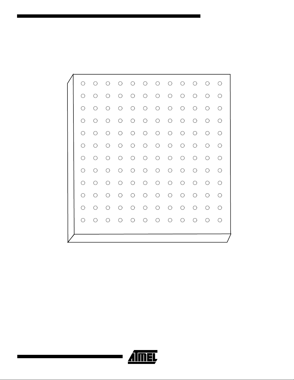
Package Outline BGA144
Figure 3. 144-ball Ball Grid Array Package
TOP VIEW
BOTTOM VIEW
Symbol
Max.
SIDE VIEW
8
AT91M43300

Atmel Headquarters Atmel Operations
Corporate Headquarters
2325 Orchard Parkway
San Jose, CA 95131
TEL (408) 441-0311
FAX (408) 487-2600
Europe
Atmel U.K., Ltd.
Coliseum Business Centre
Riverside Way
Camberley, Surrey GU15 3YL
England
TEL (44) 1276-686-677
FAX (44) 1276-686-697
Asia
Atmel Asia, Ltd.
Room 1219
Chinachem Golden Plaza
77 Mody Road Tsimhatsui
East Kowloon
Hong Kong
TEL (852) 2721-9778
FAX (852) 2722-1369
Japan
Atmel Japan K.K.
9F, Tonetsu Shinkawa Bldg.
1-24-8 Shinkawa
Chuo-ku, Tokyo 104-0033
Japan
TEL (81) 3-3523-3551
FAX (81) 3-3523-7581
Atmel Colorado Springs
1150 E. Cheyenne Mtn. Blvd.
Colorado Springs, CO 80906
TEL (719) 576-3300
FAX (719) 540-1759
Atmel Rousset
Zone Industrielle
13106 Rousset Cedex
France
TEL (33) 4-4253-6000
FAX (33) 4-4253-6001
Fax-on-Demand
North America:
1-(800) 292-8635
International:
1-(408) 441-0732
e-mail
literature@atmel.com
Web Site
http://www.atmel.com
BBS
1-(408) 436-4309
© Atmel Corporation 1999.
Atmel Corporation makes no warranty for the use of its products, other than those expressly contained in the Company’s standard warranty which is detailed in Atmel’s Terms and Conditions located on the Company’s web site. The Company assumes no responsibility for
any errors which may appear in this document, reserves the right to change devices or specifications detailed herein at any time without
notice, and does not make any commitment to update the information contained herein. No licenses to patents or other intellectual property of Atmel are granted by the Company in connection with the sale of Atmel products, expressly or by implication. Atmel’s products are
not authorized for use as critical components in life support devices or systems.
ARM, Thumb, ARM7TDMI, and ARM Powered are trademarks of ARM Limited.
All other marks bearing
Terms and product names in this document may be trademarks of others.
®
and/or ™ are registered trademarks and trademarks of Atmel Corporation.
Printed on recycled paper.
1322A–10/99/5M
 Loading...