

Page 1

BDTIC www.bdtic.com/ATMEL
Features
• Utilizes the ARM7TDMI
– High-performance 32-bit RISC Architecture
– High-density 16-bit Instruction Set
– Leader in MIPS/Watt
– Embedded ICE (In-circuit Emulation)
• 8K Bytes Internal SRAM
• Fully Programmable External Bus Interface (EBI)
– Maximum External Address Space of 64M Bytes
– Up to 8 Chip Selects
– Software Programmable 8/16-bit External Data Bus
• 8-channel Peripheral Data Controller
• 8-level Priority, Individually Maskable, Vectored Interrupt Controller
– 5 External Interrupts, Including a High-priority, Low-latency Interrupt Request
• 54 Programmable I/O Lines
• 6-channel 16-bit Timer/Counter
– 6 External Clock Inputs, 2 Multi-purpose I/O Pins per Channel
• 2 USARTs
– 2 Dedicated Peripheral Data Controller (PDC) Channels per USART
– Support for up to 9-bit Data Transfers
• 2 Master/Slave SPI Interfaces
– 2 Dedicated Peripheral Data Controller (PDC) Channels per SPI
– 8- to 16-bit Programmable Data Length
– 4 External Slave Chip Selects per SPI
• 3 System Timers
– Period Interval Timer (PIT); Real-time Timer (RTT); Watchdog Timer (WDT)
• Power Management Controller (PMC)
– CPU and Peripherals Can be Deactivated Individually
• Clock Generator with 32.768 kHz Low-power Oscillator and PLL
– Support for 38.4 kHz Crystals
– Software Programmable System Clock (up to 33 MHz)
®
• IEEE
• Fully Static Operation: 0 Hz to 33 MHz, Internal Frequency Range at V
• 2.7V to 3.6V Core and PLL Operating Voltage Range; 2.7V to 5.5V I/O Operating Voltage
• -40°C to +85°C Temperature Range
• Available in a 144-lead LQFP Package (Green) and a 144-ball BGA Package (RoHS
1149.1 JTAG Boundary Scan on All Active Pins
85°C
Range
compliant)
®
ARM® Thumb® Processor Core
DDCORE
= 3.0V,
AT91 ARM
Thumb
Microcontrollers
AT91M42800A
Rev. 1779D–ATARM–14-Apr-06
Page 2

1. Description
The AT91M42800A is a member of the Atmel AT91 16/32-bit microcontroller family, which is
based on the ARM7TDMI processor core. This processor has a high-performance 32-bit RISC
architecture with a high-density 16-bit instruction set and very low power consumption. In addition, a large number of internally banked registers result in very fast exception handling,
making the device ideal for real-time control applications. The AT91 ARM-based MCU family
also features Atmel’s high-density, in-system programmable, nonvolatile memory technology.
The AT91M42800A has a direct connection to off-chip memory, including Flash, through the
External Bus Interface.
The Power Management Controller allows the user to adjust device activity according to system requirements, and, with the 32.768 kHz low-power oscillator, enables the AT91M42800A
to reduce power requirements to an absolute minimum. The AT91M42800A is manufactured
using Atmel’s high-density CMOS technology. By combining the ARM7TDMI processor core
with on-chip SRAM and a wide range of peripheral functions including timers, serial communication controllers and a versatile clock generator on a monolithic chip, the AT91M42800A
provides a highly flexible and cost-effective solution to many compute-intensive applications.
2
AT91M42800A
1779D–ATARM–14-Apr-06
Page 3
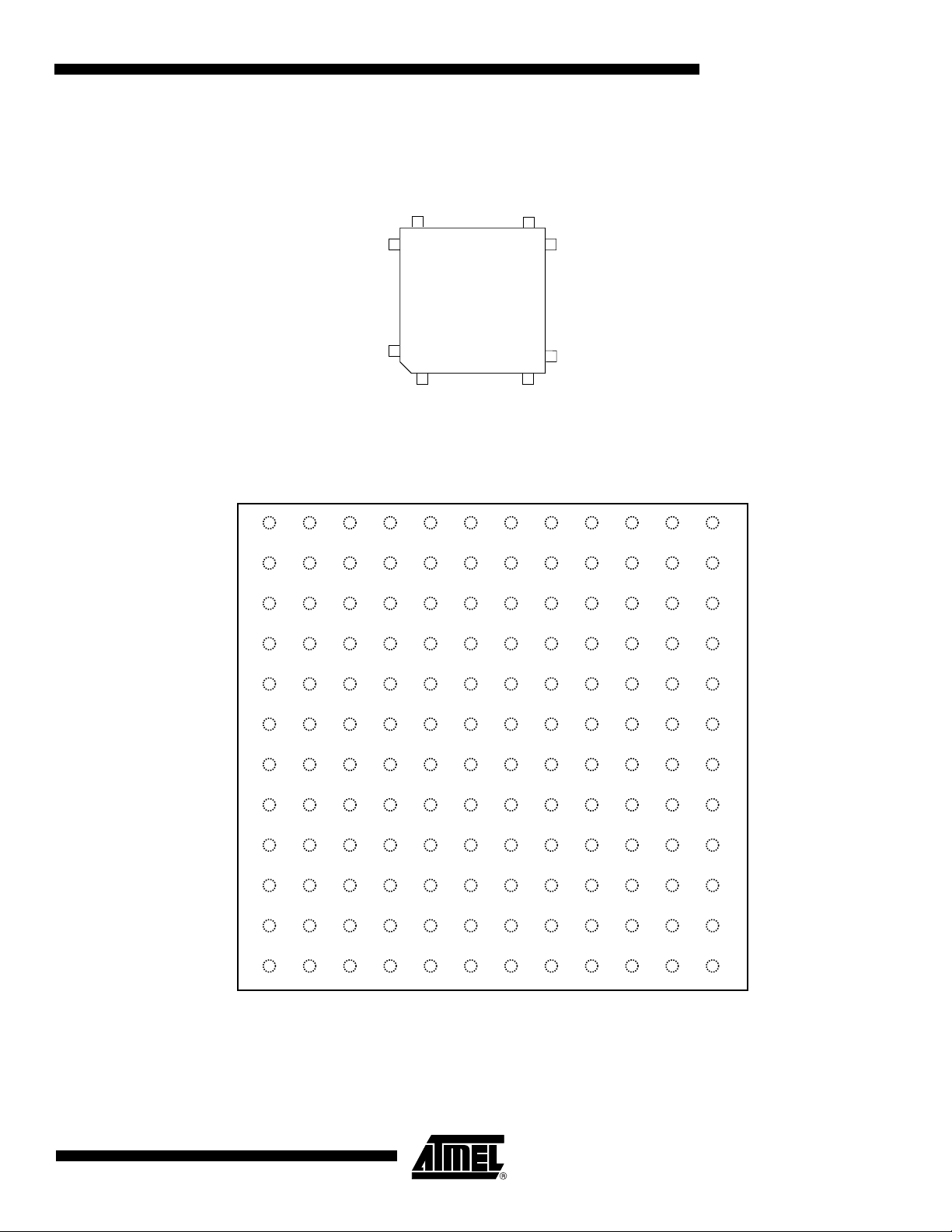
2. Pin Configuration
Figure 2-1. Pin Configuration in TQFP144 Package (Top View)
108 73
AT91M42800A
109
AT91M42800 33AI
144
136
Figure 2-2. Pin Configuration in BGA144 Package (Top View)
123456789101112
A
B
C
D
E
72
37
1779D–ATARM–14-Apr-06
F
G
H
J
K
L
M
3
Page 4

Table 1. AT91M42800A Pinout in TQFP 144 Package
Pin# Name Pin# Name Pin# Name Pin# Name
1 GND 37 GND 73 GND 109 GND
2 GND 38 GND 74 GND 110 GND
3 NLB/A0 39 D4 75 PB22/TIOA5 111 PA26
4 A1 40 D5 76 PB23/TIOB5 112 MODE0
5 A2 41 D6 77 PA0/IRQ0 113 XIN
6 A3 42 D7 78 PA1/IRQ1 114 XOUT
7 A4 43 D8 79 PA2/IRQ2 115 GND
8 A5 44 D9 80 PA3/IRQ3 116 PLLRCA
9 A6 45 D10 81 PA4/FIQ 117 VDDPLL
10 A7 46 D11 82 PA5/SCK0 118 PLLRCB
11 A8 47 D12 83 PA6/TXD0 119 VDDPLL
12 VDDIO 48 VDDIO 84 VDDIO 120 VDDIO
13 GND 49 GND 85 GND 121 GND
14 A9 50 D13 86 PA7/RXD0 122 NWDOVF
15 A10 51 D14 87 PA8/SCK1 123 PA27/BMS
16 A11 52 D15 88 PA9/TXD1/NTRI 124 MODE1
17 A12 53 PB6/TCLK0 89 PA10/RXD1 125 TMS
18 A13 54 PB7/TIOA0 90 PA11/SPCKA 126 TDI
19 A14 55 PB8/TIOB0 91 PA12/MISOA 127 TDO
20 A15 56 PB9/TCLK1 92 PA13/MOSIA 128 TCK
21 A16 57 PB10/TIOA1 93 PA14/NPCSA0/NSSA 129 NTRST
22 A17 58 PB11/TIOB1 94 PA15/NPCSA1 130 NRST
23 A18 59 PB12/TCLK2 95 PA16/NPCSA2 131 PA28
24 VDDIO 60 VDDIO 96 VDDIO 132 VDDIO
25 GND 61 GND 97 GND 133 GND
26 A19 62 PB13/TIOA2 98 PA17/NPCSA3 134 PA29/PME
27 PB2/A20/CS7 63 PB14/TIOB2 99 PA18/SPCKB 135 NWAIT
28 PB3/A21/CS6 64 PB15/TCLK3 100 PA19/MISOB 136 NOE/NRD
29 PB4/A22/CS5 65 PB16/TIOA3 101 PA20/MOSIB 137 NWE/NWR0
30 PB5/A23/CS4 66 PB17/TIOB3 102 PA21/NPCSB0/NSSB 138 NUB/NWR1
31 D0 67 PB18/TCLK4 103 PA22/NPCSB1 139 NCS0
32 D1 68 PB19/TIOA4 104 PA23/NPCSB2 140 NCS1
33 D2 69 PB20/TIOB4 105 PA24/NPCSB3 141 PB0/NCS2
34 D3 70 PB21/TCLK5 106 PA25/MCKO 142 PB1/NCS3
35 VDDCORE 71 VDDCORE 107 VDDCORE 143 VDDCORE
36 VDDIO 72 VDDIO 108 VDDIO 144 VDDIO
4
AT91M42800A
1779D–ATARM–14-Apr-06
Page 5

AT91M42800A
Table 2. AT91M42800A Pinout in BGA 144 Package
Pin# Name Pin# Name Pin# Name Pin# Name
A1 PB1/NCS3 D1 A2 G1 A17 K1 D1
A2 NCS0 D2 A3 G2 A16 K2 VDDCORE
A3 NCS1 D3 A4 G3 A11 K3 VDDIO
A4 GND D4 NWAIT G4 A13 K4 D9
A5 PLLRCB D5 PA29/PME G5 GND K5 D10
A6 GND D6 PA28 G6 GND K6 D14
A7 PLLRCA D7 TCK G7 GND K7 PB9/TCLK1
A8 GND D8 TMS G8 GND K8 PB13/TIOA2
A9 XOUT D9 MODE1 G9 PA9/TXD1/NTRI K9 PB11/TIOB1
A10 XIN D10 PA25/MCKO G10 PA10/RXD1 K10 VDDIO
A11 MODE0 D11 PA21/NPCSB0 G11 PA8/SCK1 K11 PB16/TIOA3
A12 PA22/NPCSB1 D12 PA18/SPCKB G12 PA7/RXD0 K12 PB23/TIOB5
B1 NUB/NWR1 E1 A7 H1 A18 L1 D3
B2 PB0/NCS2 E2 VDDIO H2 VDDIO L2 D2
B3 VDDCORE E3 A6 H3 A15 L3 D5
B4 NWE/NWR0 E4 A5 H4 A14 L4 D8
B5 VDDPLL E5 GND H5 A19 L5 VDDIO
B6 TDO E6 GND H6 GND L6 D13
B7 VDDPLL E7 GND H7 GND L7 PB8/TIOB0
B8 NWDOVF E8 NTRST H8 GND L8 VDDIO
B9 PA26 E9 PA13/MOSIA H9 PA6/TXD0 L9 PB17/TIOB3
B10 PA19/MISOB E10 PA16/NPCSA2 H10 PA4/FIQ L10 VDDCORE
B11 PA24/NPCSB3 E11 VDDIO H11 VDDIO L11 PB20/TIOB4
B12 PA23/NPCSB2 E12 PA17/NPCSA3 H12 PA5/SCK0 L12 PB22/TIOA5
C1 NLB/A0 F1 A8 J1 PB5/A23/CS4 M1 D4
C2 A1 F2 A12 J2 D0 M2 D6
C3 VDDIO F3 A9 J3 PB4/A22/CS5 M3 D7
C4 NOE/NRD F4 A10 J4 PB3/A21/CS6 M4 D11
C5 VDDIO F5 GND J5 PB2/A20/CS7 M5 D12
C6 NRST F6 GND J6 D15 M6 PB7/TIOA0
C7 TDI F7 GND J7 PB6/TCLK0 M7 PB12/TCLK2
C8 VDDIO F8 GND J8 PB10/TIOA1 M8 PB15/TCLK3
C9 PA27/BMS F9 PA12/MISOA J9 PA3/IRQ3 M9 PB14/TIOB2
C10 VDDIO F10 PA15/NPCSA1 J10 PA2/IRQ2 M10 PB18/TCLK4
C11 VDDCORE F11 PA11/SPCKA J11 PA0/IRQ0 M11 PB19/TIOA4
C12 PA20/MOSIB F12 PA14/NPCSA0 J12 PA1/IRQ1 M12 PB21/TCLK5
1779D–ATARM–14-Apr-06
5
Page 6

3. Pin Description
Table 3. AT91M42800A Pin Description
Module Name Function Type
A0 - A23 Address Bus Output – All valid after reset
D0 - D15 Data Bus I/O –
CS4 - CS7 Chip Select Output High A23 - A20 after reset
NCS0 - NCS3 Chip Select Output Low
NWR0 Lower Byte 0 Write Signal Output Low Used in Byte Write option
NWR1 Lower Byte 1 Write Signal Output Low Used in Byte Write option
NRD Read Signal Output Low Used in Byte Write option
EBI
NWE Write Enable Output Low Used in Byte Select option
NOE Output Enable Output Low Used in Byte Select option
NUB Upper Byte Select (16-bit SRAM) Output Low Used in Byte Select option
NLB Lower Byte Select (16-bit SRAM) Output Low Used in Byte Select option
NWAIT Wait Input Input Low
BMS Boot Mode Select Input – Sampled during reset
PME Protect Mode Enable Input High PIO-controlled after reset
Active
Level Comments
AIC
TC
USART
SPIA
SPIB
PIO
ST NWDOVF Watchdog Timer Overflow Output Low Open drain
IRQ0 - IRQ3 External Interrupt Request Input – PIO-controlled after reset
FIQ Fast External Interrupt Request Input – PIO-controlled after reset
TCLK0 - TCLK5 Timer External Clock Input – PIO-controlled after reset
TIOA0 - TIOA5 Multi-purpose Timer I/O Pin A I/O – PIO-controlled after reset
TIOB0 - TIOB5 Multi-purpose Timer I/O Pin B I/O – PIO-controlled after reset
SCK0 - SCK1 External Serial Clock I/O – PIO-controlled after reset
TXD0 - TXD1 Transmit Data Output Output – PIO-controlled after reset
RXD0 - RXD1 Receive Data Input Input – PIO-controlled after reset
SPCKA/SPCKB Clock I/O – PIO-controlled after reset
MISOA/MISOB Master In Slave Out I/O – PIO-controlled after reset
MOSIA/MOSIB Master Out Slave In I/O – PIO-controlled after reset
NSSA/NSSB Slave Select Input Low PIO-controlled after reset
NPCSA0 - NPCSA3
NPCSB0 - NPCSB3
PA0 - PA29 Programmable I/O Port A I/O – Input after reset
PB0 - PB23 Programmable I/O Port B I/O – Input after reset
Peripheral Chip Selects Output Low PIO-controlled after reset
6
AT91M42800A
1779D–ATARM–14-Apr-06
Page 7

Table 3. AT91M42800A Pin Description (Continued)
Module Name Function Type
XIN Oscillator Input or External Clock Input –
XOUT Oscillator Output Output –
CLOCK
Test and
Reset
PLLRCA RC Filter for PLL A Input –
PLLRCB RC Filter for PLL B Input –
MCKO Clock Output Output –
NRST Hardware Reset Input Input Low Schmitt trigger
MODE0 - MODE1 Mode Selection Input
TMS Test Mode Select Input – Schmitt trigger, internal pull-up
TDI Test Data In Input – Schmitt trigger, internal pull-up
AT91M42800A
Active
Level Comments
JTAG/ICE
Emulation NTRI Tri-state Mode Enable Input Low Sampled during reset
Power
TDO Test Data Out Output –
TCK Test Clock Input – Schmitt trigger, internal pull-up
NTRST Test Reset Input Input Low Schmitt trigger, internal pull-up
VDDIO I/O Power Power – 3V or 5V nominal supply
VDDCORE Core Power Power – 3V nominal supply
VDDPLL PLL Power Power – 3V nominal supply
GND Ground Ground –
1779D–ATARM–14-Apr-06
7
Page 8
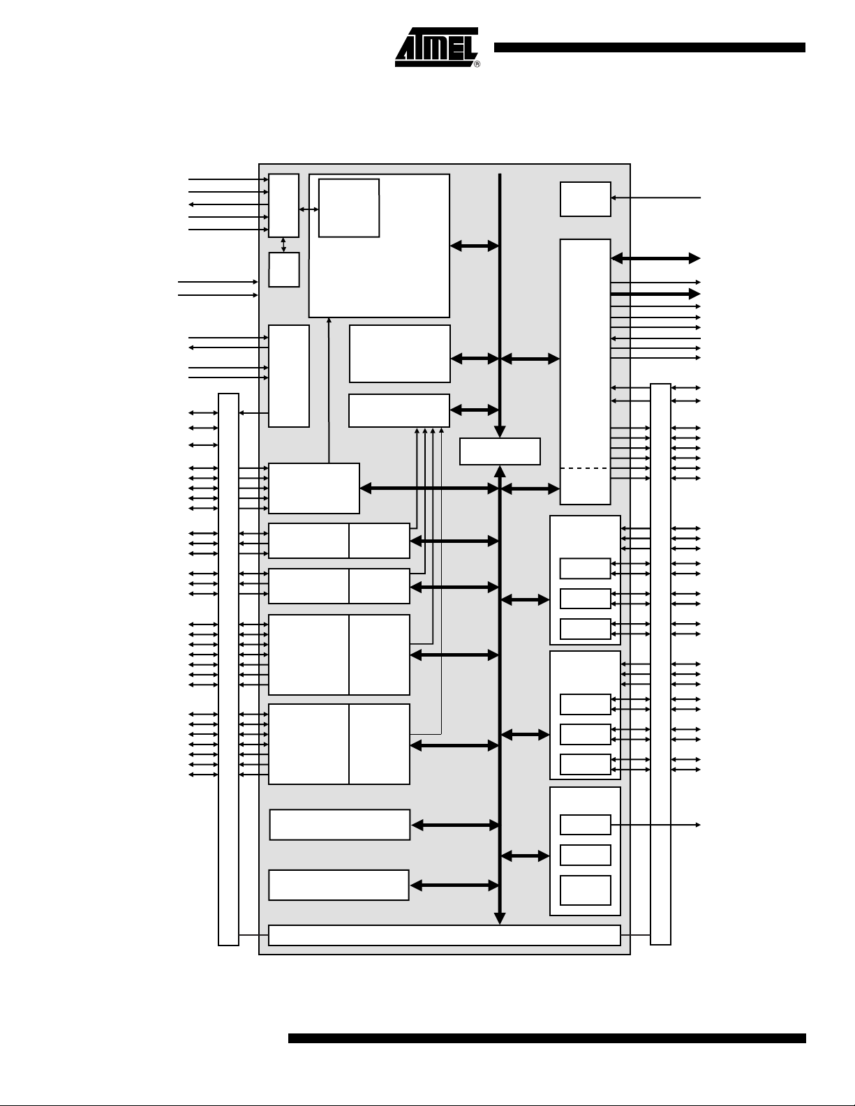
4. Block Diagram
Figure 4-1. AT91M42800A
NTRST
TMS
TDO
TDI
TCK
JTAG
Selection
Embedded
ICE
Reset
NRST
MODE0
MODE1
XIN
XOUT
PLLRCA
PLLRCB
PA25/MCKO
PA26
PA28
PA0/IRQ0
PA1/IRQ1
PA2/IRQ2
PA3/IRQ3
PA4/FIQ
PA5/SCK0
PA6/TXD0
PA7/RXD0
PA8/SCK1
PA9/TXD1/NTRI
PA10/RXD1
PA11/SPCKA
PA12/MISOA
PA13/MOSIA
PA14/NPCSA0/NSSA
PA15/NPCSA1
PA16/NPCSA2
PA17/NPCSA3
PA18/SPCKB
PA19/MISOB
PA20/MOSIB
PA21/NPCSB0/NSSB
PA22/NPCSB1
PA23/NPCSB2
PA24/NPCSB3
ARM7TDMI
JTAG
Clock
Generator
AIC: Advanced
Interrupt Controller
USART0
P
I
O
USART1
SPIA: Serial
Peripheral
Interface
SPIB: Serial
Peripheral
Interface
PMC: Power Management
Controller
Core
Internal RAM
8K Bytes
ASB
Controller
2 PDC
Channels
2 PDC
Channels
2 PDC
Channels
2 PDC
Channels
ASB
AMBA™ Bridge
APB
EBI: External
Bus Interface
EBI User
Interface
TC: Timer/
Counter
Block 0
TC0
TC1
TC2
TC: Timer/
Counter
Block 1
TC3
TC4
TC5
System
Timers
Watchdog
Real-time
P
I
O
D0-D15
A0/NLB
A1-A19
NRD/NOE
NWR0/NWE
NWR1/NUB
NWAIT
NCS0
NCS1
PA27/BMS
PA29/PME
PB0/NCS2
PB1/NCS3
PB2/A20/CS7
PB3/A21/CS6
PB4/A22/CS5
PB5/A23/CS4
PB6/TCLK0
PB9/TCLK1
PB12/TCLK2
PB7/TIOA0
PB8/TIOB0
PB10/TIOA1
PB11/TIOB1
PB13/TIOA2
PB14/TIOB2
PB15/TCLK3
PB18/TCLK4
PB21/TCLK5
PB16/TIOA3
PB17/TIOB3
PB19/TIOA4
PB20/TIOB4
PB22/TIOA5
PB23/TIOB5
NWDOVF
Chip ID
PIO: Parallel I/O Controller
8
AT91M42800A
Period
Interval
1779D–ATARM–14-Apr-06
Page 9

5. Architectural Overview
The AT91M42800A microcontroller integrates an ARM7TDMI with its embedded ICE interface, memories and peripherals. Its architecture consists of two main buses, the Advanced
System Bus (ASB) and the Advanced Peripheral Bus (APB). Designed for maximum performance and controlled by the memory controller, the ASB interfaces the ARM7TDMI processor
with the on-chip 32-bit memories, the External Bus Interface (EBI) and the AMBA
The AMBA Bridge drives the APB, which is designed for accesses to on-chip peripherals and
optimized for low power consumption.
The AT91M42800A microcontroller implements the ICE port of the ARM7TDMI processor on
dedicated pins, offering a complete, low-cost and easy-to-use debug solution for target
debugging.
5.1 Memories
The AT91M42800A microcontroller embeds up to 8K bytes of internal SRAM. The internal
memory is directly connected to the 32-bit data bus and is single-cycle accessible. This provides maximum performance of 30 MIPS at 33 MHz by using the ARM instruction set of the
processor. The on-chip memory significantly reduces the system power consumption and
improves its performance over external memory solutions.
The AT91M42800A microcontroller features an External Bus Interface (EBI), which enables
connection of external memories and application-specific peripherals. The EBI supports 8- or
16-bit devices and can use two 8-bit devices to emulate a single 16-bit device. The EBI implements the early read protocol, enabling single clock cycle memory accesses two times faster
than standard memory interfaces.
AT91M42800A
™
Bridge.
5.2 Peripherals
The AT91M42800A microcontroller integrates several peripherals, which are classified as system or user peripherals. All on-chip peripherals are 32-bit accessible by the AMBA Bridge, and
can be programmed with a minimum number of instructions. The peripheral register set is
composed of control, mode, data, status and enable/disable/status registers.
An on-chip Peripheral Data Controller (PDC) transfers data between the on-chip
USARTs/SPIs and the on- and off-chip memories without processor intervention. Most importantly, the PDC removes the processor interrupt handling overhead and significantly reduces
the number of clock cycles required for a data transfer. It can transfer up to 64K continuous
bytes without reprogramming the start address. As a result, the performance of the microcontroller is increased and the power consumption reduced.
5.2.1 System Peripherals
The External Bus Interface (EBI) controls the external memory and peripheral devices via an
8- or 16-bit data bus and is programmed through the APB. Each chip select line has its own
programming register.
The Power Management Controller (PMC) optimizes power consumption of the product by
controlling the clocking elements such as the oscillator and the PLLs, system and user peripheral clocks.
The Advanced Interrupt Controller (AIC) controls the internal sources from the internal peripherals and the five external interrupt lines (including the FIQ) to provide an interrupt and/or fast
1779D–ATARM–14-Apr-06
9
Page 10

5.2.2 User Peripherals
interrupt request to the ARM7TDMI. It integrates an 8-level priority controller, and, using the
Auto-vectoring feature, reduces the interrupt latency time.
The Parallel Input/Output Controllers (PIOA, PIOB) controls up to 54 I/O lines. It enables the
user to select specific pins for on-chip peripheral input/output functions, and general-purpose
input/output signal pins. The PIO controllers can be programmed to detect an interrupt on a
signal change from each line.
There are three embedded system timers. The Real-time Timer (RTT) counts elapsed seconds and can generate periodic or programmed interrupts. The Period Interval Timer (PIT)
can be used as a user-programmable time-base, and can generate periodic ticks. The Watchdog (WD) can be used to prevent system lock-up if the software becomes trapped in a
deadlock.
The Special Function (SF) module integrates the Chip ID and the Reset Status registers.
Two USARTs, independently configurable, enable communication at a high baud rate in synchronous or asynchronous mode. The format includes start, stop and parity bits and up to 9
data bits. Each USART also features a Time-out and a Time-guard register, facilitating the use
of the two dedicated Peripheral Data Controller (PDC) channels.
The two 3-channel, 16-bit Timer/Counters (TC) are highly-programmable and support capture
or waveform modes. Each TC channel can be programmed to measure or generate different
kinds of waves, and can detect and control two input/output signals. Each TC also has three
external clock signals.
Two independently configurable SPIs provide communication with external devices in master
or slave mode. Each has four external chip selects which can be connected to up to 15
devices. The data length is programmable, from 8- to 16-bit.
10
AT91M42800A
1779D–ATARM–14-Apr-06
Page 11

6. Associated Documentation
Table 6-1. Associated Documentation
Information Document Title
Internal architecture of processor
ARM/Thumb instruction sets
Embedded in-circuit-emulator
External memory interface mapping
Peripheral operations
Peripheral user interfaces
DC characteristics
Power consumption
Thermal and reliability chonsiderations
AC characteristics
Product overview
Ordering information
Packaging information
Soldering profile
ARM7TDMI (Thumb) Datasheet
AT91M42800A Datasheet (this document)
AT91M42800A Electrical Characteristics Datasheet
AT91M42800A Summary Datasheet
AT91M42800A
7. Product Overview
7.1 Power Supply
The AT91M42800A has three kinds of power supply pins:
• VDDCORE pins that power the chip core
• VDDIO pins that power the I/O lines
• VDDPLL pins that power the oscillator and PLL cells
VDDCORE and VDDIO pins allow core power consumption to be reduced by supplying it with
a lower voltage than the I/O lines. The VDDCORE pins must never be powered at a voltage
greater than the supply voltage applied to the VDDIO.
The VDDPLL pin is used to supply the oscillator and both PLLs. The voltage applied on these
pins is typically 3.3V, and it must not be lower than VDDCORE.
Typical supported voltage combinations are shown in the following table:
Table 1.
Pins Nominal Supply Voltages
VDDCORE 3.3V 3.0V or 3.3V
VDDIO 5.0V 3.0V or 3.3V
VDDPLL 3.3V 3.0V or 3.3V
7.2 Input/Output Considerations
After the reset, the peripheral I/Os are initialized as inputs to provide the user with maximum
flexibility. It is recommended that in any application phase, the inputs to the AT91M42800A
microcontroller be held at valid logic levels to minimize the power consumption.
1779D–ATARM–14-Apr-06
11
Page 12

7.3 Operating Modes
The AT91M42800A has two pins dedicated to defining MODE0 and MODE1 operating modes.
These pins allow the user to enter the device in Boundary Scan mode. They also allow the
user to run the processor from the on-chip oscillator output and from an external clock by
bypassing the on-chip oscillator. The last mode is reserved for test purposes. A chip reset
must be performed (NRST and NTRST) after MODE0 and/or MODE1 have been changed.
Table 7-1.
Warning: The user must take the external oscillator frequency into account so that it is consis-
tent with the minimum access time requested by the memory device used at the boot. Both the
default EBI setting (zero wait state) on Chip Select 0 (See ”Boot on NCS0” on page 29) and
the minimum access time of the boot memory are two parameters that determine this maximum frequency of the external oscillator.
7.4 Clock Generator
The AT91M42800A microcontroller embeds a 32.768 kHz oscillator that generates the Slow
Clock (SLCK). This on-chip oscillator can be bypassed by setting the correct logical level on
the MODE0 and MODE1 pins, as shown above. In this case, SLCK equals XIN.
MODE0 MODE1 Operating Mode
0 0 Normal operating mode by using the on-chip oscillator
0 1 Boundary Scan Mode
1 0 Normal operating mode by using an external clock on XIN
1 1 Reserved for test
7.5 Reset
7.5.1 NRST Pin
The AT91M42800A microcontroller has a fully static design and works either on the Master
Clock (MCK), generated from the Slow Clock by means of the two integrated PLLs, or on the
Slow Clock (SLCK).
These clocks are also provided as an output of the device on the pin MCKO, which is multiplexed with a general-purpose I/O line. While NRST is active, and after the reset, the MCKO is
valid and outputs an image of the SLCK signal. The PIO Controller must be programmed to
use this pin as standard I/O line.
Reset initializes the user interface registers to their default states as defined in the peripheral
sections of this datasheet and forces the ARM7TDMI to perform the next instruction fetch from
address zero. Except for the program counter, the ARM core registers do not have defined
reset states. When reset is active, the inputs of the AT91M42800A must be held at valid logic
levels. The EBI address lines drive low during reset. All the peripheral clocks are disabled during reset to save power.
NRST is the active low reset input. It is asserted asynchronously, but exit from reset is synchronized internally to the slow clock (SLCK). At power-up, NRST must be active until the onchip oscillator is stable. During normal operation, NRST must be active for a minimum of 10
SLCK clock cycles to ensure correct initialization.
12
AT91M42800A
1779D–ATARM–14-Apr-06
Page 13
7.5.2 NTRST Pin
AT91M42800A
The pins BMS and NTRI are sampled during the 10 SLCK clock cycles just prior to the rising
edge of NRST.
The NRST pin has no effect on the on-chip Embedded ICE logic.
The NTRST control pin initializes the selected TAP controller. The TAP controller involved in
this reset is determined according to the initial logical state applied on the JTAGSEL pin after
the last valid NRST.
In either Boundary Scan or ICE Mode, a reset can be performed from the same or different circuitry, as shown in Figure 7-1 below. But in all cases, the NTRST like the NRST signal, must
be asserted after each power-up. (See the AT91M42800A Electrical Datasheet, Atmel Lit. No.
1776, for the necessary minimum pulse assertion time.)
Figure 7-1. Separate or Common Reset Management
7.5.3 Watchdog Reset
Reset
Controller
Reset
Controller
Notes: 1. NRST and NTRST handling in Debug Mode during development.
2. NRST and NTRST handling during production.
NTRST
NRST
AT91M42800A
(1) (2)
Reset
Controller
NTRST
NRST
AT91M42800A
In order to benefit from the separation of NRST and NTRST during the debug phase of development, the user must independently manage both signals as shown in example (1) of Figure
7-1 above. However, once debug is completed, both signals are easily managed together dur-
ing production as shown in example (2) of Figure 7-1 above.
The internally generated watchdog reset has the same effect as the NRST pin, except that the
pins BMS and NTRI are not sampled. Boot mode and Tri-state mode are not updated. The
NRST pin has priority if both types of reset coincide.
7.6 Emulation Functions
7.6.1 Tri-state Mode
The AT91M42800A provides a Tri-state mode, which is used for debug purposes in order to
connect an emulator probe to an application board. In Tri-state mode the AT91M42800A continues to function, but all the output pin drivers are tri-stated.
To enter Tri-state mode, the pin NTRI must be held low during the last 10 SLCK clock cycles
before the rising edge of NRST. For normal operation, the pin NTRI must be held high during
reset, by a resistor of up to 400 kΩ. NTRI must be driven to a valid logic value during reset.
NTRI is multiplexed with Parallel I/O PA9 and USART 1 serial data transmit line TXD1.
1779D–ATARM–14-Apr-06
13
Page 14

Standard RS232 drivers generally contain internal 400 kΩ pull-up resistors. If TXD1 is con-
nected to one of these drivers, this pull-up will ensure normal operation, without the need for
an additional external resistor.
7.6.2 Embedded ICE
ARM standard embedded in-circuit emulation is supported via the JTAG/ICE port. It is connected to a host computer via an embedded ICE Interface.
Embedded ICE mode is selected when MODE1 is low.
It is not possible to switch directly between ICE and JTAG operations. A chip reset must be
performed (NRST and NTRST) after MODE0 and/or MODE1 have/has been changed. The
reset input to the embedded ICE (NTRST) is provided separately to facilitate debug of boot
programs.
7.6.3 IEEE 1149.1 JTAG Boundary Scan
IEEE 1149.1 JTAG Boundary Scan is enabled when MODE0 is low and MODE1 is high. The
functions SAMPLE, EXTEST and BYPASS are implemented. In ICE Debug mode, the ARM
core responds with a non-JTAG chip ID that identifies the core to the ICE system. This is not
IEEE 1149.1 JTAG compliant. It is not possible to switch directly between JTAG and ICE operations. A chip reset must be performed (NRST and NTRST) after MODE0 and/or MODE1
have/has been changed.
7.7 Memory Controller
The ARM7TDMI processor address space is 4G bytes. The memory controller decodes the
internal 32-bit address bus and defines three address spaces:
7.7.1 Protection Mode
7.7.2 Internal Memories
• Internal Memories in the four lowest megabytes
• Middle Space reserved for the external devices (memory or peripherals) controlled by the
EBI
• Internal Peripherals in the four highest megabytes
In any of these address spaces, the ARM7TDMI operates in little-endian mode only.
The embedded peripherals can be protected against unwanted access. The PME (Protect
Mode Enable) pin must be tied high and validated in its peripheral operation (PIO Disable) to
enable the protection mode. When enabled, any peripheral access must be done while the
ARM7TDMI is running in Privileged mode (i.e., the accesses in user mode result in an abort).
Only the valid peripheral address space is protected and requests to the undefined addresses
will lead to a normal operation without abort.
The AT91M42800A microcontroller integrates an 8-Kbyte primary internal SRAM. All internal
memories are 32 bits wide and single-clock cycle accessible. Byte (8-bit), half-word (16-bit) or
word (32-bit) accesses are supported and are executed within one cycle. Fetching Thumb or
ARM instructions is supported and internal memory can store twice as many Thumb instructions as ARM ones.
The SRAM bank is mapped at address 0x0 (after the remap command), and ARM7TDMI
exception vectors between 0x0 and 0x20 that can be modified by the software. The rest of the
14
AT91M42800A
1779D–ATARM–14-Apr-06
Page 15

7.7.3 Boot Mode Select
7.7.4 Remap Command
AT91M42800A
bank can be used for stack allocation (to speed up context saving and restoring), or as data
and program storage for critical algorithms.
The ARM reset vector is at address 0x0. After the NRST line is released, the ARM7TDMI executes the instruction stored at this address. This means that this address must be mapped in
non-volatile memory after the reset.
The input level on the BMS pin during the last 10 SLCK clock cycles before the rising edge of
the NRST selects the type of boot memory. The Boot mode depends on BMS (see Table 7-2).
The pin BMS is multiplexed with the I/O line PA27 that can be programmed after reset like any
standard PIO line.
Table 7-2. Boot Mode Select
BMS Boot Memory
1 External 8-bit memory NCS0
0 External 16-bit memory on NCS0
The ARM vectors (Reset, Abort, Data Abort, Prefetch Abort, Undefined Instruction, Interrupt,
Fast Interrupt) are mapped from address 0x0 to address 0x20. In order to allow these vectors
to be redefined dynamically by the software, the AT91M42800A microcontroller uses a remap
command that enables switching between the boot memory and the internal SRAM bank
addresses. The remap command is accessible through the EBI User Interface, by writing one
in RCB of EBI_RCR (Remap Control Register). Performing a remap command is mandatory if
access to the other external devices (connected to chip selects 1 to 7) is required. The remap
operation can only be changed back by an internal reset or an NRST assertion.
7.7.5 Abort Control
Notes: 1. NIRQ de-assertion and automatic interrupt clearing if the source is programmed as level
sensitive.
The abort signal providing a Data Abort or a Prefetch Abort exception to the ARM7TDMI is
asserted in the following cases:
• When accessing an undefined address in the EBI address space
• When the ARM7TDMI performs a misaligned access
No abort is generated when reading the internal memory or by accessing the internal peripherals, whether the address is defined or not.
When the processor performs a forbidden write access in a mode-protected peripheral register, the write is cancelled but no abort is generated.
The processor can perform word or half-word data access with a misaligned address when a
register relative load/store instruction is executed and the register contains a misaligned
address. In this case, whether the access is in write or in read, an abort is generated but the
access is not cancelled.
The Abort Status Register traces the source that caused the last abort. The address and the
type of abort are stored in registers of the External Bus Interface.
1779D–ATARM–14-Apr-06
15
Page 16

7.8 External Bus Interface
The External Bus Interface handles the accesses between addresses 0x0040 0000 and
0xFFC0 0000. It generates the signals that control access to the external devices, and can be
configured from eight 1-Mbyte banks up to four 16-Mbyte banks. In all cases it supports byte,
half-word and word aligned accesses.
For each of these banks, the user can program:
• Number of wait states
• Number of data float times (wait time after the access is finished to prevent any bus
contention in case the device takes too long in releasing the bus)
• Data bus width (8-bit or 16-bit)
• With a 16-bit wide data bus, the user can program the EBI to control one 16-bit device
(Byte Access Select mode) or two 8-bit devices in parallel that emulate a
16-bit memory (Byte Write Access mode).
The External Bus Interface features also the Early Read Protocol, configurable for all the
devices, that significantly reduces access time requirements on an external device.
8. Peripherals
The AT91M42800A peripherals are connected to the 32-bit wide Advanced Peripheral Bus.
Peripheral registers are only word accessible. Byte and half-word accesses are not supported.
If a byte or a half-word access is attempted, the memory controller automatically masks the
lowest address bits and generates a word access.
Each peripheral has a 16-Kbyte address space allocated (the AIC only has a 4-Kbyte address
space).
8.0.1 Peripheral Registers
The following registers are common to all peripherals:
• Control Register – Write-only register that triggers a command when a one is written to the
• Mode Register – read/write register that defines the configuration of the peripheral. Usually
• Data Registers – read and/or write register that enables the exchange of data between the
• Status Register – Read-only register that returns the status of the peripheral.
• Enable/Disable/Status Registers are shadow command registers. Writing a one in the
Unused bits in the peripheral registers are shown as “–” and must be written at 0 for upward
compatibility. These bits read 0.
corresponding position at the appropriate address. Writing a zero has no effect.
has a value of 0x0 after a reset.
processor and the peripheral.
Enable Register sets the corresponding bit in the Status Register. Writing a one in the
Disable Register resets the corresponding bit and the result can be read in the Status
Register. Writing a bit to zero has no effect. This register access method maximizes the
efficiency of bit manipulation, and enables modification of a register with a single noninterruptible instruction, replacing the costly read-modify-write operation.
8.0.2 Peripheral Interrupt Control
The Interrupt Control of each peripheral is controlled from the status register using the interrupt mask. The status register bits are ANDed to their corresponding interrupt mask bits and
16
AT91M42800A
1779D–ATARM–14-Apr-06
Page 17

the result is then ORed to generate the Interrupt Source signal to the Advanced Interrupt
Controller.
The interrupt mask is read in the Interrupt Mask Register and is modified with the Interrupt
Enable Register and the Interrupt Disable Register. The enable/disable/status (or mask)
makes it possible to enable or disable peripheral interrupt sources with a non-interruptible single instruction. This eliminates the need for interrupt masking at the AIC or Core level in realtime and multi-tasking systems.
8.0.3 Peripheral Data Controller
The AT91M42800A has an 8-channel PDC dedicated to the two on-chip USARTs and to the
two on-chip SPIs. One PDC channel is connected to the receiving channel and one to the
transmitting channel of each peripheral.
The user interface of a PDC channel is integrated in the memory space of each USART channel and in the memory space of each SPI. It contains a 32-bit address pointer register and a
16-bit count register. When the programmed data is transferred, an end-of-transfer interrupt is
generated by the corresponding peripheral. See Section 17. ”USART: Universal Synchro-
nous/Asynchronous Receiver/Transmitter” on page 121 and Section 19. ”SPI: Serial
Peripheral Interface” on page 177 for more details on PDC operation and programming.
AT91M42800A
8.1 System Peripherals
8.1.1 PMC: Power Management Controller
The AT91M42800A’s Power Management Controller optimizes the power consumption of the
device. The PMC controls the clocking elements such as the oscillator and the PLLs, and the
System and the Peripheral Clocks. It also controls the MCKO pin and permits to the user to
select four different signals to be driven on this pin.
The AT91M42800A has the following clock elements:
• The oscillator providing a clock that depends on the crystal fundamental frequency
connected between the XIN and XOUT pins
• PLL A providing a low-to-middle frequency clock range
• PLL B providing a middle-to-high frequency range
• The Clock prescaler
• The ARM Processor Clock controller
• The Peripheral Clock controller
• The Master Clock Output controller
The on-chip low-power oscillator together with the PLL-based frequency multiplier and the
prescaler results in a programmable clock between 500 Hz and 66 MHz. It is the responsibility
of the user to make sure that the PMC programming does not result in a clock over the acceptable limits.
8.1.2 ST: System Timer
1779D–ATARM–14-Apr-06
The System Timer module integrates three different free-running timers:
• A Period Interval Timer setting the base time for an Operating System.
17
Page 18

• A Watchdog Timer that is built around a 16-bit counter, and is used to prevent system lockup if the software becomes trapped in a deadlock. It can generate an internal reset or
interrupt, or assert an active level on the dedicated pin NWDOVF.
• A Real-time Timer counting elapsed seconds.
These timers count using the Slow Clock. Typically, this clock has a frequency of 32768 Hz.
8.1.3 AIC: Advanced Interrupt Controller
The AT91M42800A has an 8-level priority, individually maskable, vectored interrupt controller.
This feature substantially reduces the software and real-time overhead in handling internal
and external interrupts.
The interrupt controller is connected to the NFIQ (fast interrupt request) and the NIRQ (standard interrupt request) inputs of the ARM7TDMI processor. The processor’s NFIQ line can
only be asserted by the external fast interrupt request input: FIQ. The NIRQ line can be
asserted by the interrupts generated by the on-chip peripherals and the external interrupt
request lines: IRQ0 to IRQ3.
The 8-level priority encoder allows the customer to define the priority between the different
NIRQ interrupt sources.
Internal sources are programmed to be level sensitive or edge triggered. External sources can
be programmed to be positive or negative edge triggered or high- or low-level sensitive.
8.1.4 PIO: Parallel I/O Controller
The AT91M42800A has 54 programmable I/O lines. I/O lines are multiplexed with an external
signal of a peripheral to optimize the use of available package pins. These lines are controlled
by two separate and identical PIO Controllers called PIOA and PIOB. Each PIO controller also
provides an internal interrupt signal to the Advanced Interrupt Controller and insertion of a simple input glitch filter on any of the PIO pins.
8.1.5 SF: Special Function
The AT91M42800A provides registers that implement the following special functions.
• Chip Identification
• RESET Status
8.2 User Peripherals
8.2.1 USART: Universal Synchronous/ Asynchronous Receiver Transmitter
The AT91M42800A provides two identical, full-duplex, universal synchronous/asynchronous
receiver/transmitters that interface to the APB and are connected to the Peripheral Data
Controller.
The main features are:
• Programmable Baud Rate Generator with External or Internal Clock, as well as Slow Clock
• Parity, Framing and Overrun Error Detection
• Line Break Generation and Detection
• Automatic Echo, Local Loopback and Remote Loopback channel modes
• Multi-drop mode: Address Detection and Generation
18
AT91M42800A
1779D–ATARM–14-Apr-06
Page 19

8.2.2 TC: Timer/Counter
The AT91M42800A features two Timer/Counter blocks, each containing three identical 16-bit
Timer/Counter channels. Each channel can be independently programmed to perform a wide
range of functions including frequency measurement, event counting, interval measurement,
pulse generation, delay timing and pulse-width modulation.
Each Timer/Counter (TC) channel has 3 external clock inputs, 5 internal clock inputs, and 2
multi-purpose input/output signals that can be configured by the user. Each channel drives an
internal interrupt signal that can be programmed to generate processor interrupts via the AIC
(Advanced Interrupt Controller).
The Timer/Counter block has two global registers that act upon all three TC channels. The
Block Control Register allows the three channels to be started simultaneously with the same
instruction. The Block Mode Register defines the external clock inputs for each Timer/Counter
channel, allowing them to be chained.
Each Timer/Counter block operates independently and has a complete set of block and channel registers.
AT91M42800A
• Interrupt Generation
• Two Dedicated Peripheral Data Controller channels
• 5-, 6-, 7-, 8- and 9-bit character length
8.2.3 SPI: Serial Peripheral Interface
The AT91M42800A includes two SPIs that provide communication with external devices in
Master or Slave mode. They are independent, and are referred to by the letters A and B. Each
SPI has four external chip selects that can be connected to up to 15 devices. The data length
is programmable from 8- to 16-bit.
1779D–ATARM–14-Apr-06
19
Page 20

9. Memory Map
Figure 9-1. AT91M42800A Memory Map before Remap Command
Address Function Size Protection
0xFFFFFFFF
(1)
Abort Control
0xFFC00000
0xFFBFFFFF
0x00400000
0x003FFFFF
0x00300000
0x002FFFFF
On-chip
Peripherals
Reserved
On-chip SRAM
Reserved
On-chip
Device
4M Bytes
1M Byte
1M Byte
Privileged
No
No
Ye s
No
No
20
0x00200000
0x001FFFFF
0x00100000
0x000FFFFF
0x00000000
Note: 1. The ARM core modes are defined in the ARM7TDMI Datasheet. Privileged is a non-user
AT91M42800A
Reserved
On-chip
Device
External
Devices Selected
by NCS0
1M Byte
1M Byte
No
No
No
No
mode. The protection is active only if Protect mode is enabled.
1779D–ATARM–14-Apr-06
Page 21

Figure 9-2. AT91M42800A Memory Map after Remap Command
Address Function Size Protection
0xFFFFFFFF
On-chip
Peripherals
0xFFC00000
0xFFBFFFFF
4M Bytes
Privileged
AT91M42800A
(1)
Abort Control
Ye s
0x00400000
0x003FFFFF
0x00300000
0x002FFFFF
0x00200000
0x001FFFFF
External
Devices
(up to 8)
Reserved
Reserved
On-chip
Device
Reserved
On-chip
Device
Up to 8 Devices
Programmable Page Size
1, 4, 16, 64M Bytes
1M Byte No No
1M Byte No No
1M Byte
No
No
Ye s
No
1779D–ATARM–14-Apr-06
0x00100000
0x000FFFFF
0x00000000
On-chip RAM
1M Byte
No
No
Note: 1. The ARM core modes are defined in the ARM7TDMI Datasheet. Privileged is a non-user
mode. The protection is active only if Protect mode is enabled.
21
Page 22

10. Peripheral Memory Map
Figure 10-1. AT91M42800A Peripheral Memory Map
Address Peripheral Peripheral Name Size Protection
0xFFFFFFFF
0xFFFFF000
0xFFFFEFFF
0xFFFFC000
0xFFFFBFFF
0xFFFF8000
0xFFFF7FFF
0xFFFF4000
0xFFFF3FFF
0xFFFF0000
0xFFFEFFFF
0xFFFEC000
0xFFFEBFFF
0xFFFD8000
0xFFFD7FFF
0xFFFD4000
0xFFFD3FFF
0xFFFD0000
0xFFFCFFFF
0xFFFCC000
0xFFFCBFFF
0xFFFC8000
0xFFFC7FFF
0xFFFC4000
0xFFFC3FFF
0xFFFC0000
0xFFFBFFFF
0xFFF04000
0xFFF03FFF
0xFFF00000
0xFFEFFFFF
0xFFF04000
0xFFE03FFF
0xFFE00000
0xFFDFFFFF
0xFFD00000
Note: 1. The ARM core modes are defined in the ARM7TDMI Datasheet. Privileged is a non-user
AIC
ST
PMC
PIOB
PIOA
TC1
TC0
SPIB
SPIA
USART1
USART0
SF
EBI
Advanced Interrupt Controller
Reserved
System Timer
Power Management Controller
Parallel I/O Controller B
Parallel I/O Controller A
Reserved
Timer Counter 1
Channels 3, 4 and 5
Timer Counter 0
Channels 0,1 and 2
Serial Peripheral Interface B
Serial Peripheral Interface A
Universal Synchronous/
Asynchronous
Receiver/Transmitter 1
Universal Synchronous/
Asynchronous
Receiver/Transmitter 0
Reserved
Special Function
Reserved
External Bus Interface
Reserved
4K Bytes
16K Bytes
16K Bytes
16K Bytes
16K Bytes
16K Bytes
16K Bytes
16K Bytes
16K Bytes
16K Bytes
16K Bytes
16K Bytes
16K Bytes
mode. The protection is active only if Protect mode is enabled.
Privileged
Privileged
Privileged
Privileged
Privileged
Privileged
Privileged
Privileged
Privileged
Privileged
Privileged
Privileged
Privileged
22
AT91M42800A
1779D–ATARM–14-Apr-06
Page 23

11. EBI: External Bus Interface
The EBI handles the access requests performed by the ARM core or the PDC. It generates the
signals that control the access to the external memory or peripheral devices. The EBI is fully
programmable and can address up to 64M bytes. It has eight chip selects and a 24-bit address
bus, the upper four bits of which are multiplexed with a chip select.
The 16-bit data bus can be configured to interface with 8- or 16-bit external devices. Separate
read and write control signals allow for direct memory and peripheral interfacing.
The EBI supports different access protocols allowing single clock cycle memory accesses.
The main features are:
• External memory mapping
• Up to 8 chip select lines
• 8- or 16-bit data bus
• Byte write or byte select lines
• Remap of boot memory
• Two different read protocols
• Programmable wait state generation
• External wait request
• Programmable data float time
The EBI User Interface is described on page 48.
AT91M42800A
11.1 External Memory Mapping
The memory map associates the internal 32-bit address space with the external 24-bit
address bus.
The memory map is defined by programming the base address and page size of the external
memories (see registers EBI_CSR0 to EBI_CSR7 in Section 11.13 ”EBI User Interface” on
page 48). Note that A0 - A23 is only significant for 8-bit memory; A1 - A23 is used for 16-bit
memory.
If the physical memory device is smaller than the programmed page size, it wraps around and
appears to be repeated within the page. The EBI correctly handles any valid access to the
memory device within the page (see Figure 11-1 on page 24).
In the event of an access request to an address outside any programmed page, an abort signal is generated. Two types of abort are possible: instruction prefetch abort and data abort.
The corresponding exception vector addresses are 0x0000000C and 0x00000010, respectively. It is up to the system programmer to program the error handling routine to use in case of
an abort (see the ARM7TDMI datasheet for further information).
The chip selects can be defined to the same base address and an access to the overlapping
address space asserts both NCS lines. The Chip Select Register, having the smaller number,
defines the characteristics of the external access and the behaviour of the control signals.
1779D–ATARM–14-Apr-06
23
Page 24

11.2 Abort Status
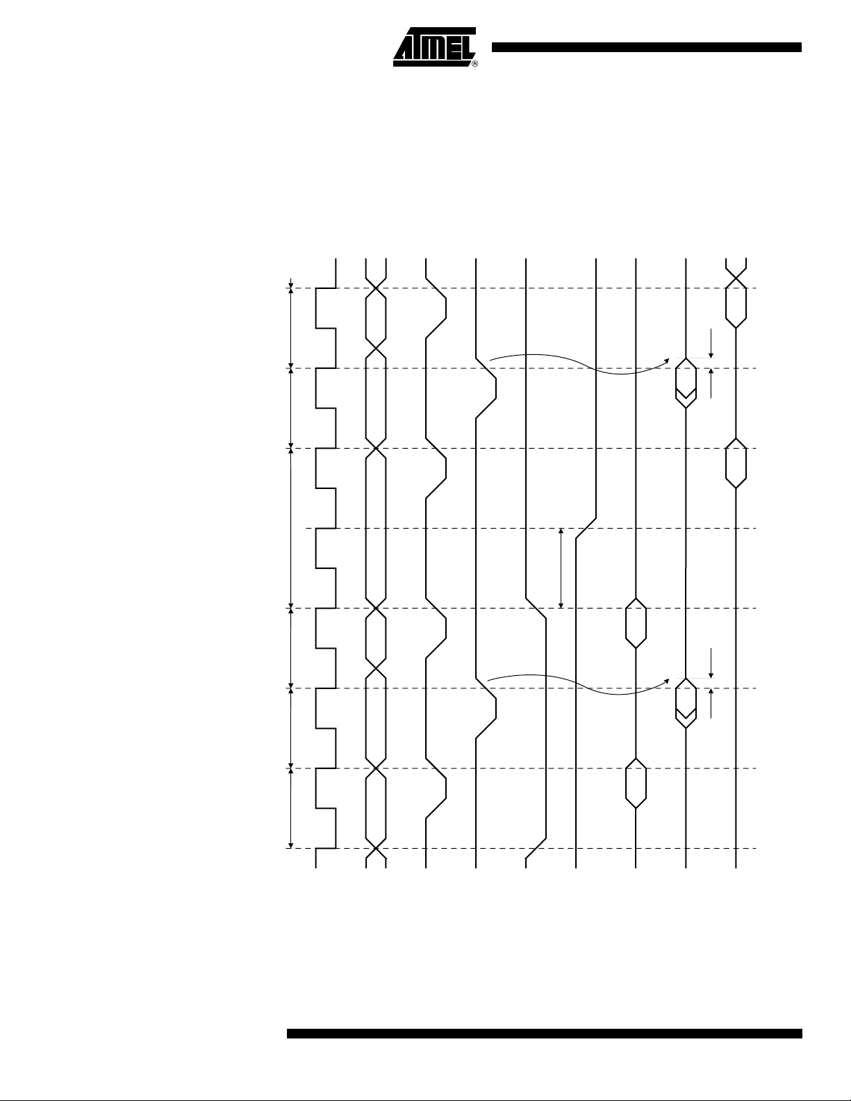
Figure 11-1. External Memory Smaller than Page Size
Base + 4M Bytes
1M Byte Device
1M Byte Device
Memory
Map
1M Byte Device
1M Byte Device
Low
Low
Low
Low
Hi
Base + 3M Bytes
Hi
Base + 2M Bytes
Hi
Base + 1M Byte
Hi
Base
Repeat 3
Repeat 2
Repeat 1
When an abort is generated, the EBI_AASR (Abort Address Status Register) and the
EBI_ASR (Abort Status Register) provide the details of the source causing the abort. Only the
last abort is saved and registers are left in the last abort status. After the reset, the registers
are initialized to 0.
The following are saved:
In EBI_AASR:
• The address at which the abort is generated
In EBI_ASR:
• Whether or not the processor has accessed an undefined address in the EBI address
space
• Whether or not the processor required an access at a misaligned address
• The size of the access (byte, word or half-word)
• The type of the access (read, write or code fetch)
11.3 EBI Behavior During Internal Accesses
When the ARM core performs accesses in the internal memories or the embedded peripherals, the EBI signals behave as follows:
• The address lines remain at the level of the last external access.
• The data bus is tri-stated.
• The control signals remain in an inactive state.
24
AT91M42800A
1779D–ATARM–14-Apr-06
Page 25

AT91M42800A
11.4 Pin Description
Table 11-1. External Bus Interface Pin Description
Name Description Type
A0 - A23 Address bus Output
D0 - D15 Data bus I/O
NCS0 - NCS3 Active low chip selects Output
CS4 - CS7 Active high chip selects Output
NRD Read Enable Output
NWR0 - NWR1 Lower and upper write enable Output
NOE Output enable Output
NWE Write enable Output
NUB, NLB Upper and lower byte select Output
NWAIT Wait request Input
PME Protection Mode Enabled Input
Table 11-2. EBI Multiplexed Signals
Multiplexed Signals Functions
A23 - A20 CS4 - CS7 Allows from 4 to 8 chip select lines to be used
A0 NLB 8- or 16-bit data bus
NRD NOE Byte-write or byte select access
NWR0 NWE Byte-write or byte select access
NWR1 NUB Byte-write or byte select access
11.5 Chip Select Lines
The EBI provides up to eight chip select lines:
• Chip select lines NCS0 - NCS3 are dedicated to the EBI (not multiplexed).
• Chip select lines CS4 - CS7 are multiplexed with the top four address lines A23 - A20.
By exchanging address lines for chip select lines, the user can optimize the EBI to suit the
external memory requirements: more external devices or larger address range for each
device.
The selection is controlled by the ALE field in EBI_MCR (Memory Control Register). The following combinations are possible:
A20, A21, A22, A23 (configuration by default)
A20, A21, A22, CS4
A20, A21, CS5, CS4
A20, CS6, CS5, CS4
CS7, CS6, CS5, CS4
1779D–ATARM–14-Apr-06
25
Page 26
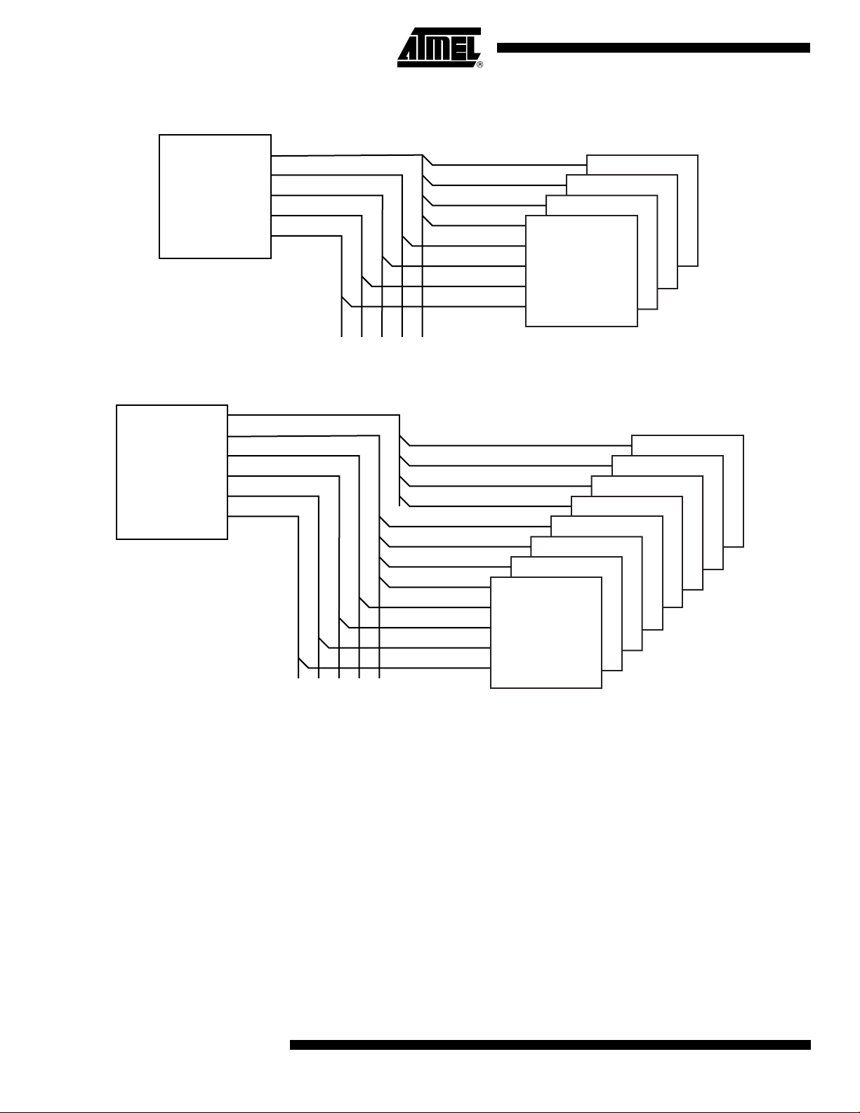
Figure 11-2. Memory Connections for Four External Devices
(1)
NCS0 - NCS3
NRD
EBI
NWRx
A0 - A23
D0 - D15
Notes: 1. For four external devices, the maximum address space per device is 16M bytes.
Figure 11-3. Memory Connections for Eight External Devices
CS4 - CS7
NCS0 - NCS3
NRD
EBI
NWRx
A0 - A19
D0 - D15
(1)
NCS0
8 or 16
NCS2
NCS1
NCS0
8 or 16
NCS3
NCS2
NCS1
Memory Enable
Memory Enable
Output Enable
Write Enable
A0 - A19
D0 - D15 or D0 - D7
NCS3
Memory Enable
Output Enable
Write Enable
A0 - A23
D0 - D15 or D0 - D7
CS5
CS4
Memory Enable
Memory Enable
Memory Enable
Memory Enable
CS7
CS6
Memory Enable
Memory Enable
Memory Enable
Memory Enable
Memory Enable
11.6 Data Bus Width
26
AT91M42800A
Notes: 1. For eight external devices, the maximum address space per device is 1M byte.
A data bus width of 8 or 16 bits can be selected for each chip select. This option is controlled
by the DBW field in the EBI_CSR (Chip Select Register) for the corresponding chip select.
Figure 11-4 shows how to connect a 512K x 8-bit memory on NCS2.
1779D–ATARM–14-Apr-06
Page 27

Figure 11-4. Memory Connection for an 8-bit Data Bus
AT91M42800A
EBI
D0 - D7
D8 - D15
A1 - A18
A0
NWR1
NWR0
NRD
NCS2
D0 - D7
A1 - A18
A0
Write Enable
Output Enable
Memory Enable
Figure 11-5 shows how to connect a 512K x 16-bit memory on NCS2.
Figure 11-5. Memory Connection for a 16-bit Data Bus
EBI
D0 - D7
D8 - D15
A1 - A19
NLB
NUB High Byte Enable
NWE
NOE
NCS2
D0 - D7
D8 - D15
A0 - A18
Low Byte Enable
Write Enable
Output Enable
Memory Enable
11.7 Byte Write or Byte Select Access
Each chip select with a 16-bit data bus can operate with one of two different types of write
access:
• Byte Write Access supports two byte write and a single read signal.
• Byte Select Access selects upper and/or lower byte with two byte select lines, and separate
read and write signals.
This option is controlled by the BAT field in the EBI_CSR (Chip Select Register) for the corresponding chip select.
Byte Write Access is used to connect 2 x 8-bit devices as a 16-bit memory page.
• The signal A0/NLB is not used.
• The signal NWR1/NUB is used as NWR1 and enables upper byte writes.
• The signal NWR0/NWE is used as NWR0 and enables lower byte writes.
• The signal NRD/NOE is used as NRD and enables half-word and byte reads.
Figure 11-6 shows how to connect two 512K x 8-bit devices in parallel on NCS2.
1779D–ATARM–14-Apr-06
27
Page 28
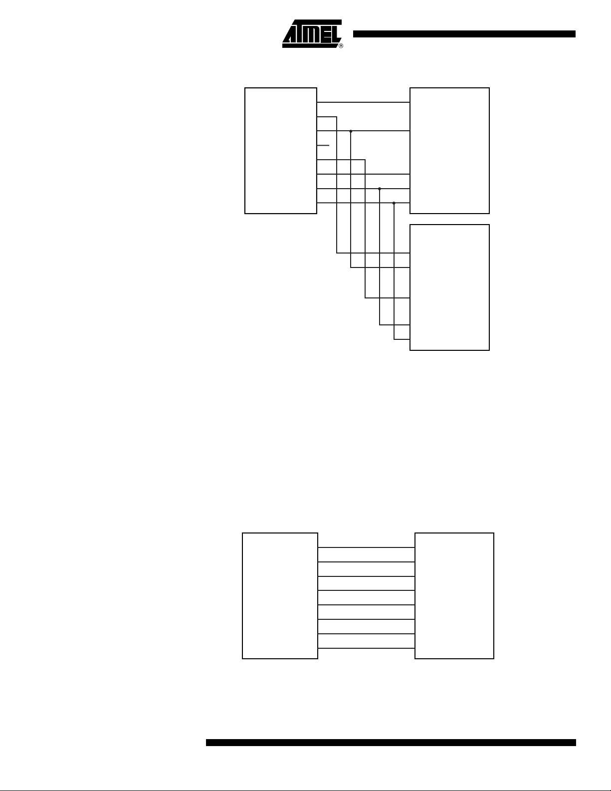
Figure 11-6. Memory Connection for 2 x 8-bit Data Buses
EBI
D0 - D7
D8 - D15
A1 - A19
A0
NWR1
NWR0
NRD
NCS2
D0 - D7
A0 - A18
Write Enable
Read Enable
Memory Enable
D8 - D15
A0 - A18
Write Enable
Read Enable
Memory Enable
Byte Select Access is used to connect 16-bit devices in a memory page.
• The signal A0/NLB is used as NLB and enables the lower byte for both read and write
operations.
• The signal NWR1/NUB is used as NUB and enables the upper byte for both read and write
operations.
• The signal NWR0/NWE is used as NWE and enables writing for byte or half-word.
• The signal NRD/NOE is used as NOE and enables reading for byte or half-word.
Figure 11-7 shows how to connect a 16-bit device with byte and half-word access (e.g., 16-bit
SRAM) on NCS2.
28
Figure 11-7. Connection for a 16-bit Data Bus with Byte and Half-word Access
Figure 11-8 shows how to connect a 16-bit device without byte access (e.g., Flash) on NCS2.
AT91M42800A
EBI
D0 - D7
D8 - D15
A1 - A19
NLB
NUB High Byte Enable
NWE
NOE
NCS2
D0 - D7
D8 - D15
A0 - A18
Low Byte Enable
Write Enable
Output Enable
Memory Enable
1779D–ATARM–14-Apr-06
Page 29
AT91M42800A
Figure 11-8. Connection for a 16-bit Data Bus without Byte Write Capability
11.8 Boot on NCS0
EBI
D0 - D7
D8 - D15
A1 - A19
NLB
NUB
NWE
NOE
NCS2
D0 - D7
D8 - D15
A0 - A18
Write Enable
Output Enable
Memory Enable
Depending on the device and the BMS pin level during the reset, the user can select either an
8-bit or 16-bit external memory device connected on NCS0 as the Boot memory. In this case,
EBI_CSR0 (Chip Select Register 0) is reset at the following configuration for chip select 0:
• 8 wait states (WSE = 0 - wait states disabled)
• 8-bit or 16-bit data bus width, depending on BMS
Byte access type and number of data float time are set to Byte Write Access and 0,
respectively.
Before the remap command, the user can modify the chip select 0 configuration, programming
the EBI_CSR0 with the exact Boot memory characteristics. The base address becomes effective after the remap command.
11.9 Read Protocols
Warning: In the internal oscillator bypass mode described in ”Operating Modes” on page 12,
the user must take the external oscillator frequency into account according to the minimum
access time on the boot memory device.
As illustration, the following table gives examples of oscillator frequency limits according to the
time access without using NWAIT pin at the boot.
Chip Select Assertion to Output Data Valid
Maximum Delay in Read Cycle (t
110 7
90 9
70 11
55 14
25 24
Note: Values take only tCE into account.
in ns)
CE
External Oscillator
Frequency Limit (MHz)
The EBI provides two alternative protocols for external memory read access: standard and
early read. The difference between the two protocols lies in the timing of the NRD (read cycle)
waveform.
1779D–ATARM–14-Apr-06
29
Page 30
The protocol is selected by the DRP field in EBI_MCR (Memory Control Register) and is valid
for all memory devices. Standard read protocol is the default protocol after reset.
Note: In the following waveforms and descriptions, NRD represents NRD and NOE since the two sig-
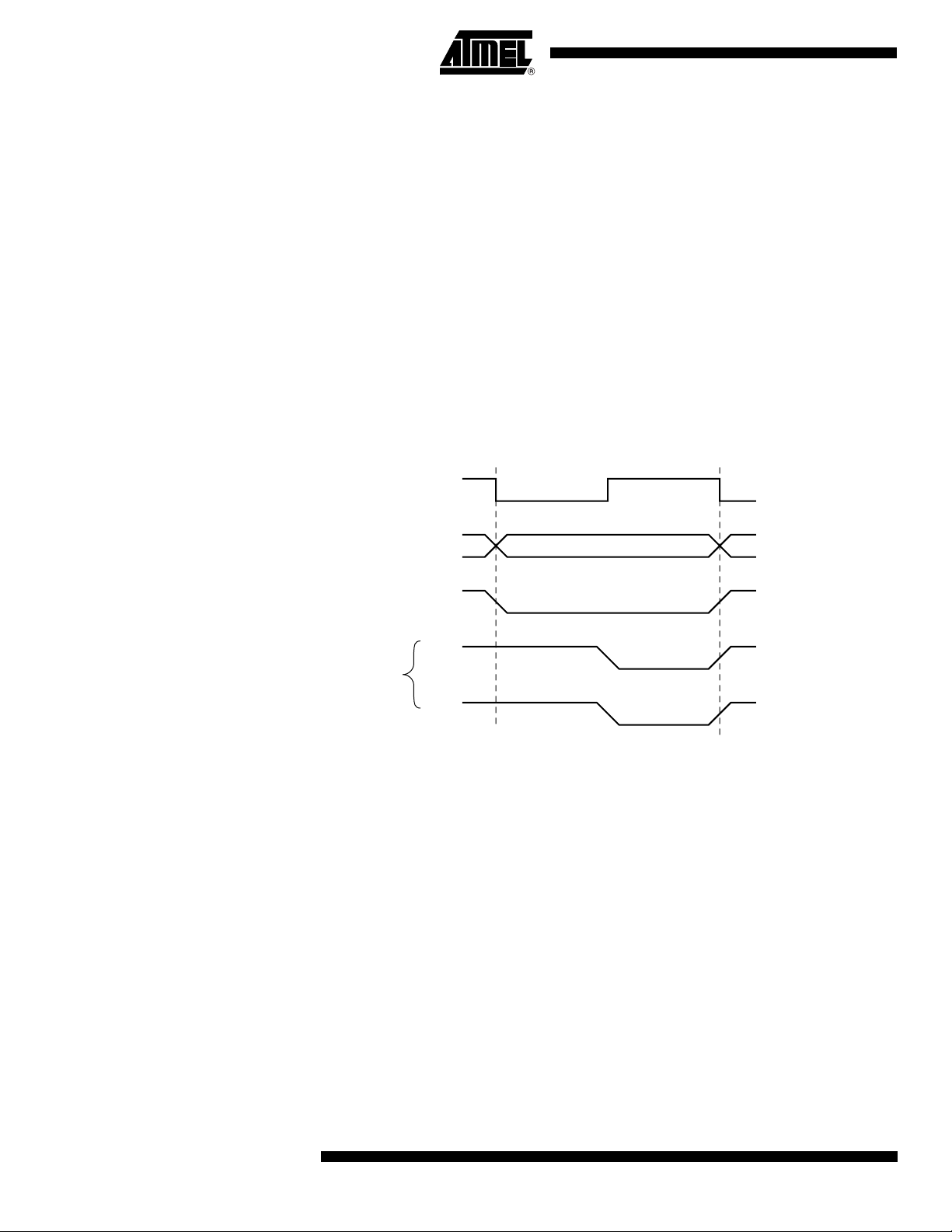
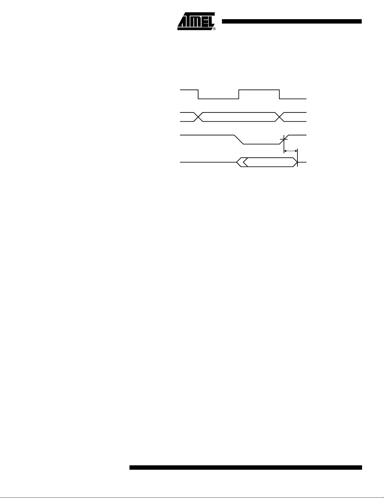
11.9.1 Standard Read Protocol
Standard read protocol implements a read cycle in which NRD and NWE are similar. Both are
active during the second half of the clock cycle. The first half of the clock cycle allows time to
ensure completion of the previous access as well as the output of address and NCS before the
read cycle begins.
During a standard read protocol, external memory access, NCS is set low and ADDR is valid
at the beginning of the access while NRD goes low only in the second half of the master clock
cycle to avoid bus conflict (see Figure 11-9).
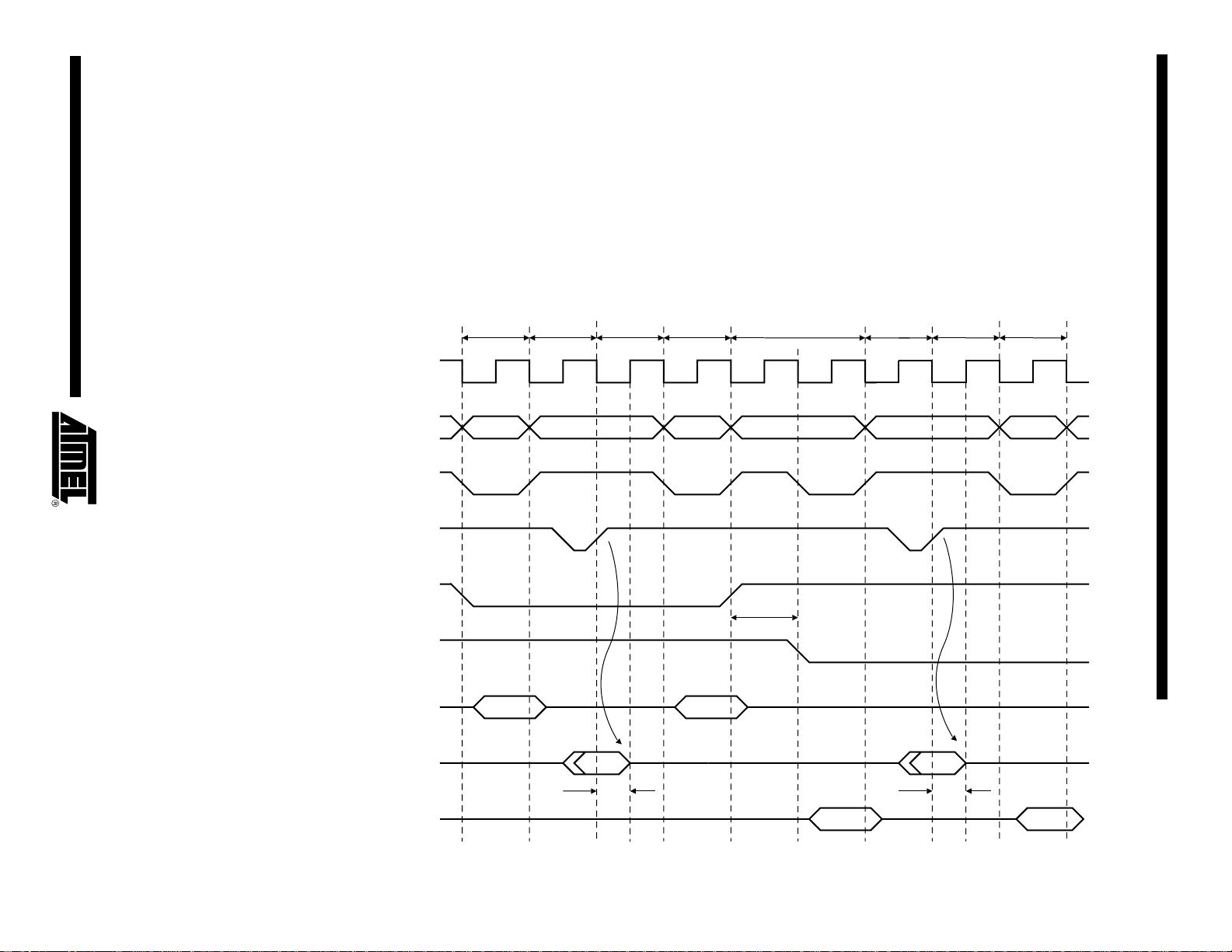
Figure 11-9. Standard Read Protocol
nals have the same waveform. Likewise, NWE represents NWE, NWR0 and NWR1 unless
NWR0 and NWR1 are otherwise represented. ADDR represents A0 - A23 and/or
A1 - A23.
MCKI
ADDR
NWE is the same in both protocols. NWE always goes low in the second half of the master
clock cycle (see Figure 11-11 on page 31).
11.9.2 Early Read Protocol
Early read protocol provides more time for a read access from the memory by asserting NRD
at the beginning of the clock cycle. In the case of successive read cycles in the same memory,
NRD remains active continuously. Since a read cycle normally limits the speed of operation of
the external memory system, early read protocol can allow a faster clock frequency to be
used. However, an extra wait state is required in some cases to avoid contentions on the
external bus.
NCS
NRD
or
NWE
30
AT91M42800A
1779D–ATARM–14-Apr-06
Page 31
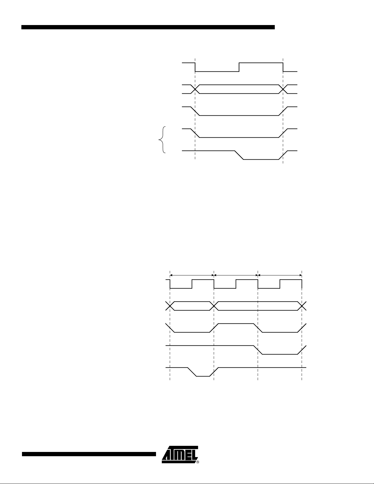
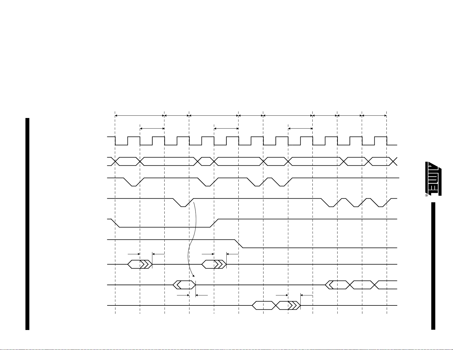
Figure 11-10. Early Read Protocol
11.9.3 Early Read Wait State
In early read protocol, an early read wait state is automatically inserted when an external write
cycle is followed by a read cycle to allow time for the write cycle to end before the subsequent
read cycle begins (see Figure 11-11). This wait state is generated in addition to any other programmed wait states (i.e., data float wait).
AT91M42800A
MCKI
ADDR
NCS
NRD
or
NWE
No wait state is added when a read cycle is followed by a write cycle, between consecutive
accesses of the same type or between external and internal memory accesses.
Early read wait states affect the external bus only. They do not affect internal bus timing.
Figure 11-11. Early Read Wait State
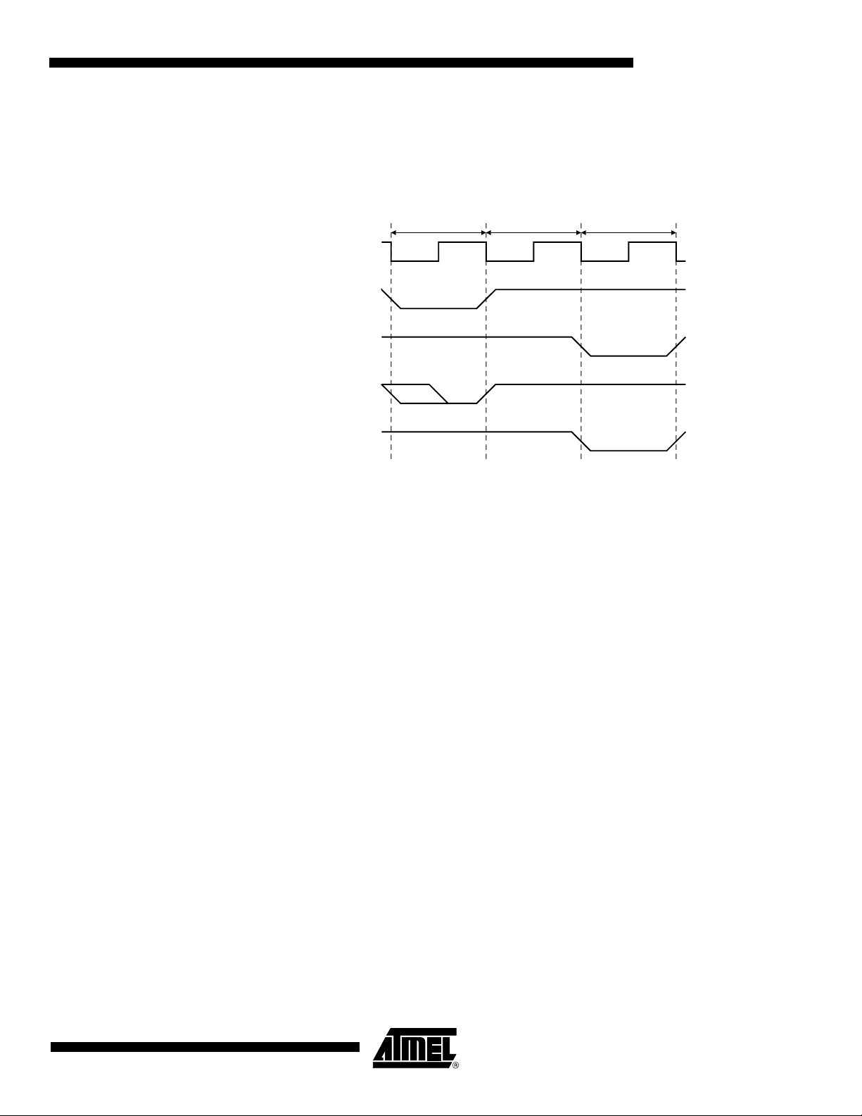
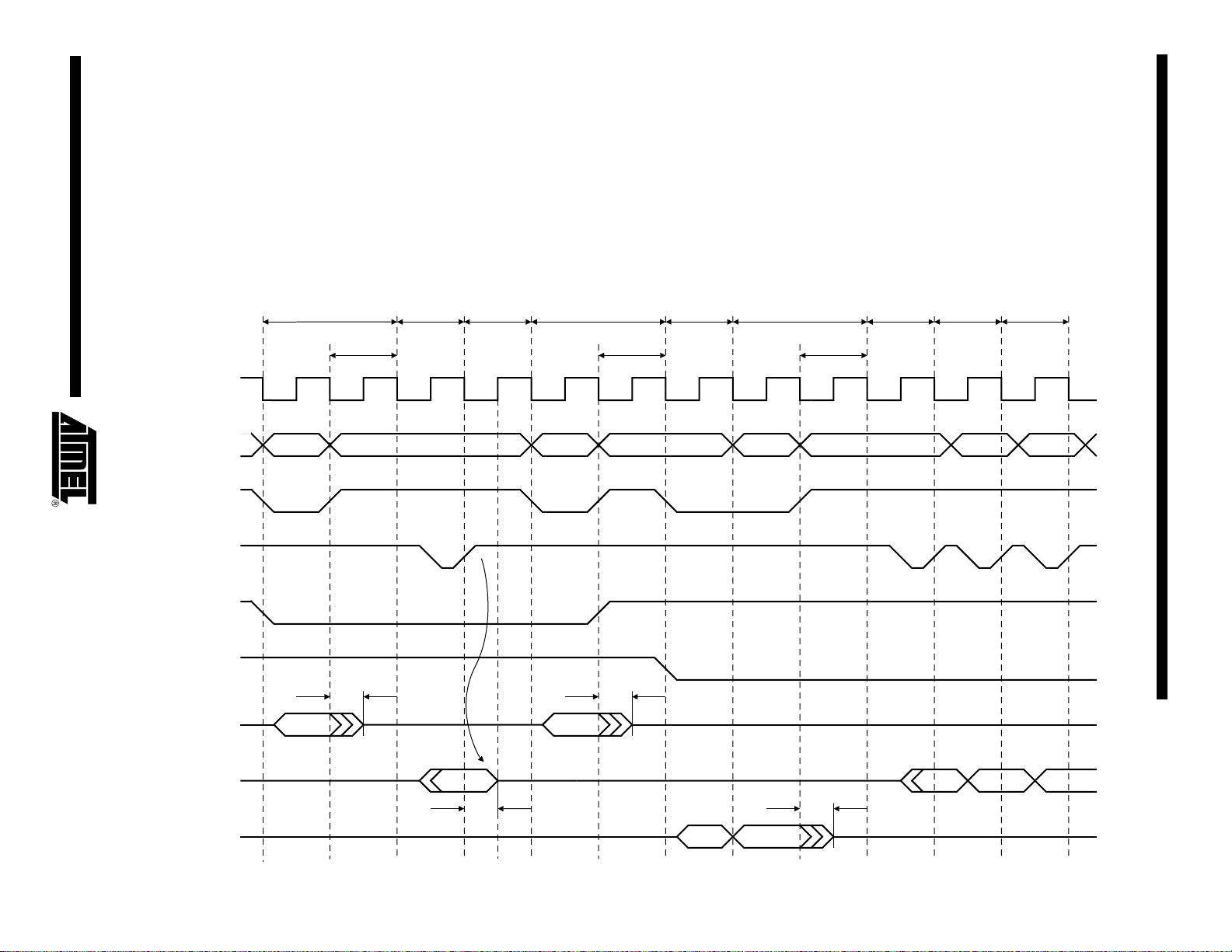
11.10 Write Data Hold Time
During write cycles in both protocols, output data becomes valid after the falling edge of the
NWE signal and remains valid after the rising edge of NWE, as illustrated in Figure 11-12. The
external NWE waveform (on the NWE pin) is used to control the output data timing to guarantee this operation.
MCKI
ADDR
NCS
NRD
NWE
Write Cycle
Early Read Wait
Read Cycle
1779D–ATARM–14-Apr-06
31
Page 32
11.11 Wait States
It is therefore necessary to avoid excessive loading of the NWE pins, which could delay the
write signal too long and cause a contention with a subsequent read cycle in standard
protocol.
Figure 11-12. Data Hold Time
MCKI
ADDR
NWE
Data Output
In early read protocol the data can remain valid longer than in standard read protocol due to
the additional wait cycle which follows a write access.
The EBI can automatically insert wait states. The different types of wait states are listed below:
• Standard wait states
• Data float wait states
• External wait states
• Chip select change wait states
• Early Read wait states (as described in ”Read Protocols” on page 29)
11.11.1 Standard Wait States
Each chip select can be programmed to insert one or more wait states during an access on
the corresponding device. This is done by setting the WSE field in the corresponding
EBI_CSR. The number of cycles to insert is programmed in the NWS field in the same
register.
Below is the correspondence between the number of standard wait states programmed and
the number of cycles during which the NWE pulse is held low:
For each additional wait state programmed, an additional cycle is added.
0 wait states 1/2 cycle
1 wait state 1 cycle
32
AT91M42800A
1779D–ATARM–14-Apr-06
Page 33
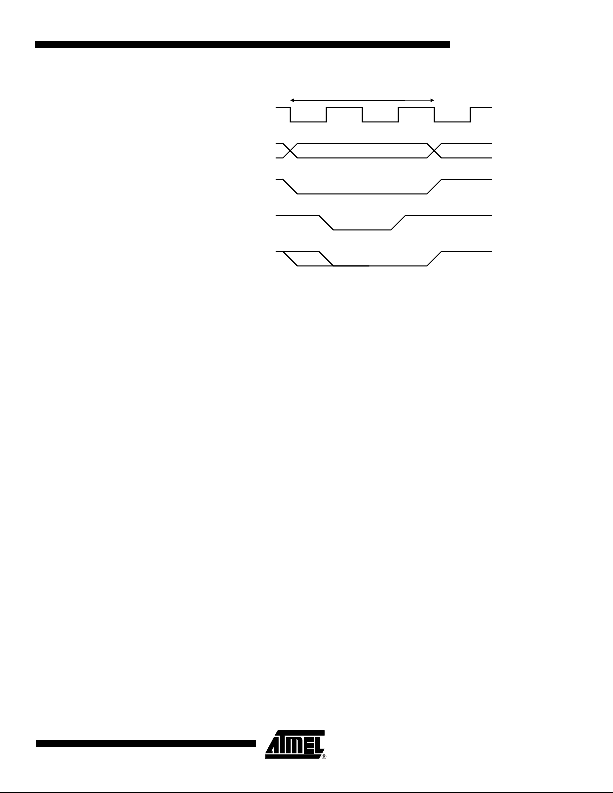
Figure 11-13. One Wait State Access
MCKI
ADDR
NCS
NWE
AT91M42800A
1 Wait State Access
Notes: 1. Early Read Protocol
11.11.2 Data Float Wait State
Some memory devices are slow to release the external bus. For such devices, it is necessary
to add wait states (data float waits) after a read access before starting a write access or a read
access to a different external memory.
The data float output time (t
field of the EBI_CSR register for the corresponding chip select. The value (0 - 7 clock cycles)
indicates the number of data float waits to be inserted and represents the time allowed for the
data output to go high impedance after the memory is disabled.
Data float wait states do not delay internal memory accesses. Hence, a single access to an
external memory with long t
memory.
The EBI keeps track of the programmed external data float time during internal accesses, to
ensure that the external memory system is not accessed while it is still busy.
Internal memory accesses and consecutive accesses to the same external memory do not
have added data float wait states.
NRD
2. Standard Read Protocol
(1)
) for each external memory device is programmed in the TDF
DF
DF
(2)
will not slow down the execution of a program from internal
1779D–ATARM–14-Apr-06
33
Page 34
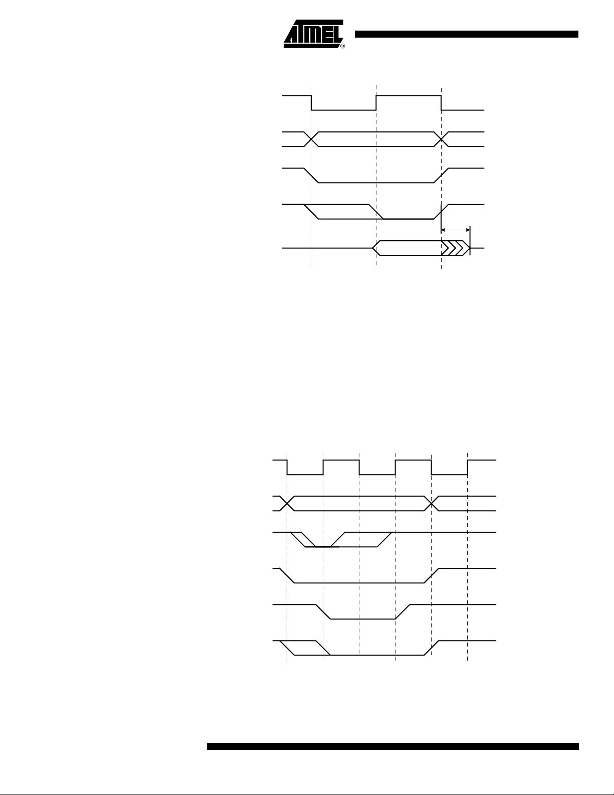
Figure 11-14. Data Float Output Time
MCKI
ADDR
NCS
11.11.3 External Wait
NRD
D0-D15
(1) (2)
t
DF
Notes: 1. Early Read Protocol
2. Standard Read Protocol
The NWAIT input can be used to add wait states at any time. NWAIT is active low and is
detected on the rising edge of the clock.
If NWAIT is low at the rising edge of the clock, the EBI adds a wait state and changes neither
the output signals nor its internal counters and state. When NWAIT is de-asserted, the EBI finishes the access sequence.
The NWAIT signal must meet setup and hold requirements on the rising edge of the clock.
Figure 11-15. External Wait
MCKI
34
Notes: 1. Early Read Protocol
AT91M42800A
ADDR
NWAIT
NCS
NWE
NRD
(1)
2. Standard Read Protocol
(2)
1779D–ATARM–14-Apr-06
Page 35
11.11.4 Chip Select Change Wait States
A chip select wait state is automatically inserted when consecutive accesses are made to two
different external memories (if no wait states have already been inserted). If any wait states
have already been inserted, (e.g., data float wait) then none are added.
Figure 11-16. Chip Select Wait
AT91M42800A
Mem 1 Chip Select Wait Mem 2
MCKI
NCS1
NCS2
NRD
NWE
Notes: 1. Early Read Protocol
2. Standard Read Protocol
(1) (2)
1779D–ATARM–14-Apr-06
35
Page 36
11.12 Memory Access Waveforms
Figures 11-17 through 11-20 show examples of the two alternative protocols for external
memory read access.
Figure 11-17. Standard Read Protocol without t
Read Mem 2
Write Mem 2
Read Mem 2
DF
WHDX
t
Read Mem 1
Write Mem 1
Read Mem 1
MCKI
A0-A23
NRD
NWE
chip select
change wait
NCS1
NCS2
D0 - D15 (Mem1)
D0 - D15 (AT91)
WHDX
t
D0 - D15 (Mem 2)
36
AT91M42800A
1779D–ATARM–14-Apr-06
Page 37
1779D–ATARM–14-Apr-06
Figure 11-18. Early Read Protocol without t
MCKI
A0 - A23
NRD
NWE
NCS1
NCS2
D0 - D15 (Mem 1)
D0 - D15 (AT91)
Read
Mem 1
Write
Mem 1
Early Read
Wait Cycle
Read
Mem 1
Read
Mem 2
Chip Select
Change Wait
Write
Mem 2
Early Read
Wait Cycle
Read
Mem 2
DF
AT91M42800A
37
D0 - D15 (Mem 2)
Long t
WHDX
long t
WHDX
Page 38
38
AT91M42800A
Figure 11-19. Standard Read Protocol with t
MCKI
A0 - A23
NRD
NWE
NCS1
NCS2
D0 - D15 (Mem 1)
Read Mem 1
Data
Float Wait
t
DF
Write
Mem 1
Read Mem 1
Data
Float Wait
t
DF
Read
Mem 2
Read
Mem 2
Float Wait
Data
Write
Mem 2
Write
Mem 2
Write
Mem 2
DF
1779D–ATARM–14-Apr-06
D0 - D15 (AT91)
t
WHDX
t
DF
D0 - 15 (Mem 2)
Page 39
1779D–ATARM–14-Apr-06
Figure 11-20. Early Read Protocol with t
MCKI
A0 - A23
NRD
NWE
NCS1
NCS2
D0 - D15 (Mem 1)
Read Mem 1
Data
Float Wait
t
DF
Write
Mem 1
Early
Read Wait
Read Mem 1
Data
Float Wait
t
DF
Read
Mem 2
Read Mem 2
Data
Float Wait
Write
Mem 2
Write
Mem 2
Write
Mem 2
DF
AT91M42800A
39
D0 - D15 (AT91)
D0 - D15 (Mem 2)
t
WHDX
t
DF
Page 40

Figures 11-21 through 11-27 show the timing cycles and wait states for read and write access
to the various AT91M42800A external memory devices. The configurations described are
shown in the following table:
Table 11-3. Memory Access Waveforms
Figure Number Number of Wait States Bus Width Size of Data Transfer
11-21 0 16 Word
11-22 1 16 Word
11-23 1 16 Half-word
11-24 0 8 Word
11-25 1 8 Half-word
11-26 1 8 Byte
11-27 0 16 Byte
40
AT91M42800A
1779D–ATARM–14-Apr-06
Page 41
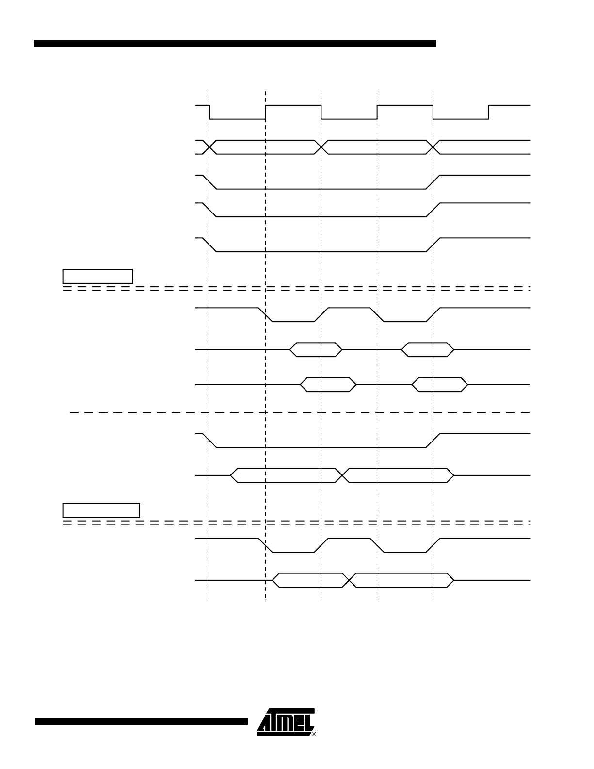
Figure 11-21. 0 Wait States, 16-bit Bus Width, Word Transfer
MCKI
AT91M42800A
READ ACCESS
· Standard Protocol
· Early Protocol
A1 - A23
NCS
NLB
NUB
NRD
D0 - D15
Internal Bus
ADDR
ADDR+1
B2B1 B
X X B2 B
1
4 B3
B4 B3 B2 B
1
WRITE ACCESS
· Byte Write/
Byte Select Option
NRD
NWE
B2 B
1
B2 B1
B4 B
B
3 D0 - D15
B
3 D0 - D15
4
1779D–ATARM–14-Apr-06
41
Page 42

Figure 11-22. 1 Wait State, 16-bit Bus Width, Word Transfer
1 Wait State 1 Wait State
MCKI
READ ACCESS
· Standard Protocol
A1 - A23
NCS
NLB
NUB
NRD
D0 - D15
Internal Bus
ADDR
B2 B1
X X B
2 B1
ADDR+1
B4 B3
B4 B3 B2 B
1
· Early Protocol
WRITE ACCESS
· Byte Write/
Byte Select Option
NRD
D0 - D15
NWE
D0 - D15
B2B
B4B
B4B
3
3
B2B
1
1
42
AT91M42800A
1779D–ATARM–14-Apr-06
Page 43

Figure 11-23. 1 Wait State, 16-bit Bus Width, Half-word Transfer
1 Wait State
MCKI
A1 - A23
NCS
NLB
NUB
READ ACCESS
· Standard Protocol
NRD
AT91M42800A
· Early Protocol
WRITE ACCESS
· Byte Write/
Byte Select Option
D0 - D15
Internal Bus
NRD
D0 - D15
NWE
D0 - D15
B2 B
B2 B
B2 B
1
X X B2 B
1
1
1
1779D–ATARM–14-Apr-06
43
Page 44

Figure 11-24. 0 Wait States, 8-bit Bus Width, Word Transfer
MCKI
A0 - A23
NCS
READ ACCESS
· Standard Protocol
NRD
D0 - D15
Internal Bus
· Early Protocol
NRD
D0 - D15
ADDR
X B
X X X B
X B
ADDR+1
1
1
1
X B
X X B2 B
X B
ADDR+2 ADDR+3
2
1
2
X B
X B3 B2 B
X B
3
1
3
X B
4
B4 B3 B2 B
X B
4
1
44
WRITE ACCESS
NWR0
NWR1
D0 - D15
AT91M42800A
X B
1
X B
2
X B
3
X B
4
1779D–ATARM–14-Apr-06
Page 45

Figure 11-25. 1 Wait State, 8-bit Bus Width, Half-word Transfer
AT91M42800A
MCKI
A0 - A23
NCS
READ ACCESS
· Standard Protocol
NRD
D0 - D15
Internal Bus
· Early Protocol
NRD
1Wait State
ADDR
X B
X X X B
1
1 Wait State
1
ADDR+1
X B
2
X X B2 B
1
D0 - D15
WRITE ACCESS
NWR0
NWR1
D0 - D15
X B
X B
1
1
X B
X B
2
2
1779D–ATARM–14-Apr-06
45
Page 46

Figure 11-26. 1 Wait State, 8-bit Bus Width, Byte Transfer
1 Wait State
MCKI
A0 - A23
NCS
READ ACCESS
· Standard Protocol
NRD
· Early Protocol
WRITE ACCESS
D0 - D15
Internal Bus
NRD
D0 - D15
NWR0
NWR1
D0 - D15
X B
X B
XB1
X X X B
1
1
1
46
AT91M42800A
1779D–ATARM–14-Apr-06
Page 47

Figure 11-27. 0 Wait States, 16-bit Bus Width, Byte Transfer
MCKI
X X X
A1 - A23
ADDR
0 ADDR X X X 0
AT91M42800A
Internal Address
READ ACCESS
· Standard Protocol
D0 - D15
Internal Bus
· Early Protocol
NCS
NLB
NUB
NRD
NRD
ADDR X X X 0 ADDR X X X 1
X B
1
X X X B
1
B2X
X X B2X
WRITE ACCESS
· Byte Write Option
· Byte Select Option
1779D–ATARM–14-Apr-06
D0 - D15
NWR0
NWR1
D0 - D15
NWE
XB
B1B
1
1
B2X
B2B
2
47
Page 48

11.13 EBI User Interface
The EBI is programmed using the registers listed in Table 11-4. The Remap Control Register
(EBI_RCR) controls exit from Boot mode (see ”Boot on NCS0” on page 29). The Memory Control Register (EBI_MCR) is used to program the number of active chip selects and data read
protocol. Eight Chip Select Registers (EBI_CSR0 to EBI_CSR7) are used to program the
parameters for the individual external memories. Each EBI_CSR must be programmed with a
different base address, even for unused chip selects.
The Abort Status registers indicate the access address (EBI_AASR) and the reason for the
abort (EBI_ASR).
Base Address: 0xFFE00000 (Code Label EBI_BASE)
Table 11-4. EBI Memory Map
Offset Register Name Access Reset State
0x00 Chip Select Register 0 EBI_CSR0 Read/Write 0x0000201E
0x0000201D
0x04 Chip Select Register 1 EBI_CSR1 Read/Write 0x10000000
0x08 Chip Select Register 2 EBI_CSR2 Read/Write 0x20000000
0x0C Chip Select Register 3 EBI_CSR3 Read/Write 0x30000000
0x10 Chip Select Register 4 EBI_CSR4 Read/Write 0x40000000
0x14 Chip Select Register 5 EBI_CSR5 Read/Write 0x50000000
(1)
(2)
0x18 Chip Select Register 6 EBI_CSR6 Read/Write 0x60000000
0x1C Chip Select Register 7 EBI_CSR7 Read/Write 0x70000000
0x20 Remap Control Register EBI_RCR Write-only –
0x24 Memory Control Register EBI_MCR Read/Write 0
0x28 Reserved – – –
0x2C Reserved – – –
0x30 Abort Status Register EBI_ASR Read-only 0x0
0x34 Address Abort Status
Register
Notes: 1. 8-bit boot (if BMS is detected high)
2. 16-bit boot (if BMS is detected low)
EBI_AASR Read-only 0x0
48
AT91M42800A
1779D–ATARM–14-Apr-06
Page 49

AT91M42800A
11.14 EBI Chip Select Register
Register Name: EBI_CSR0 - EBI_CSR7
Access Type: Read/Write
Reset Value: See Table 11-4
Absolute Address: 0xFFE00000 - 0xFFE0001C
31 30 29 28 27 26 25 24
BA
23 22 21 20 19 18 17 16
BA ––––
15 14 13 12 11 10 9 8
––CSENBAT TDF PAGES
76543210
PAGES – WSE NWS DBW
• DBW: Data Bus Width
DBW Data Bus Width Code Label: EBI_DBW
00 Reserved –
0 1 16-bit data bus width EBI_DBW_16
1 0 8-bit data bus width EBI_DBW_8
11 Reserved –
• NWS: Number of Wait States
This field is valid only if WSE is set.
NWS Number of Standard Wait States Code Label: EBI_NWS
0 0 0 1 EBI_NWS_1
0 0 1 2 EBI_NWS_2
0 1 0 3 EBI_NWS_3
0 1 1 4 EBI_NWS_4
1 0 0 5 EBI_NWS_5
1 0 1 6 EBI_NWS_6
1 1 0 7 EBI_NWS_7
1 1 1 8 EBI_NWS_8
• WSE: Wait State Enable (Code Label EBI_WSE)
0 = Wait state generation is disabled. No wait states are inserted.
1 = Wait state generation is enabled.
1779D–ATARM–14-Apr-06
49
Page 50

• PAGES: Page Size
PAGES Page Size Active Bits in Base Address Code Label: EBI_PAGES
0 0 1M Byte 12 Bits (31 - 20) EBI_PAGES_1M
0 1 4M Bytes 10 Bits (31 - 22) EBI_PAGES_4M
1 0 16M Bytes 8 Bits (31 - 24) EBI_PAGES_16M
1 1 64M Bytes 6 Bits (31 - 26) EBI_PAGES_64M
• TDF: Data Float Output Time
TDF Number of Cycles Added after the Transfer Code Label: EBI_TDF
000 0 EBI_TDF_0
001 1 EBI_TDF_1
010 2 EBI_TDF_2
011 3 EBI_TDF_3
100 4 EBI_TDF_4
101 5 EBI_TDF_5
110 6 EBI_TDF_6
111 7 EBI_TDF_7
• BAT: Byte Access Type
BAT Selected BAT Code Label: EBI_BAT
0 Byte-write access type EBI_BAT_BYTE_WRITE
1 Byte-select access type EBI_BAT_BYTE_SELECT
• CSEN: Chip Select Enable (Code Label EBI_CSEN)
0 = Chip select is disabled.
1 = Chip select is enabled.
• BA: Base Address (Code Label EBI_BA)
These bits contain the highest bits of the base address. If the page size is larger than 1M byte, the unused bits of the base
address are ignored by the EBI decoder.
50
AT91M42800A
1779D–ATARM–14-Apr-06
Page 51

AT91M42800A
11.15 EBI Remap Control Register
Register Name: EBI_RCR
Access Type: Write-only
Absolute Address: 0xFFE00020
31 30 29 28 27 26 25 24
––––––––
23 22 21 20 19 18 17 16
––––––––
15 14 13 12 11 10 9 8
––––––––
76543210
–––––––RCB
• RCB: Remap Command Bit (Code Label EBI_RCB)
0 = No effect.
1 = Cancels the remapping (performed at reset) of the page zero memory devices.
1779D–ATARM–14-Apr-06
51
Page 52

11.16 EBI Memory Control Register
Register Name: EBI_MCR
Access Type: Read/Write
Reset Value: See Table 11-4
Absolute Address: 0xFFE00024
31 30 29 28 27 26 25 24
––––––––
23 22 21 20 19 18 17 16
––––––––
15 14 13 12 11 10 9 8
––––––––
76543210
– – – DRP – ALE
• ALE: Address Line Enable
This field determines the number of valid address lines and the number of valid chip select lines.
ALE Valid Address Bits Maximum Addressable Space Valid Chip Select Code Label: EBI_ALE
0 X X A20, A21, A22, A23 16M Bytes None EBI_ALE_16M
1 0 0 A20, A21, A22 8M Bytes CS4 EBI_ALE_8M
1 0 1 A20, A21 4M Bytes CS4, CS5 EBI_ALE_4M
1 1 0 A20 2M Bytes CS4, CS5, CS6 EBI_ALE_2M
1 1 1 None 1M Byte CS4, CS5, CS6, CS7 EBI_ALE_1M
• DRP: Data Read Protocol
DRP Selected DRP Code Label: EBI_DRP
0 Standard read protocol for all external memory devices enabled EBI_DRP_STANDARD
1 Early read protocol for all external memory devices enabled EBI_DRP_EARLY
52
AT91M42800A
1779D–ATARM–14-Apr-06
Page 53

AT91M42800A
11.17 Abort Status Register
Register Name: EBI_ASR
Access Type: Read-only
Offset: 0x30
Reset Value: 0x0
31 30 29 28 27 26 25 24
––––––––
23 22 21 20 19 18 17 16
––––––––
15 14 13 12 11 10 9 8
– – PDC ARM ABTTYP ABTSZ
76543210
––––––MISADDUNDADD
• UNDADD: Undefined Address Abort Status
0 = The last abort is not due to the access of an undefined address in the EBI address space.
1 = The last abort is due to the access of an undefined address in the EBI address space.
• MISADD: Misaligned Address Abort Status
0 = During the last aborted access, the address required by the core was not unaligned.
1 = During the last aborted access, the address required by the core was unaligned.
• ABTSZ: Abort Size Status
This bit provides the size of the aborted access required by the core.
ABTSZ Abort Size
00 Byte
01 Half-word
10 Word
11 Reserved
• ABTTYP: Abort Type Status
This bit provides the type of the aborted access required by the core.
ABTTYP Abort Size
00 Data read
0 1 Data write
1 0 Code fetch
11 Reserved
• ARM: Abort Induced by the ARM Core
0 = The last abort is not due to the ARM core.
1 = The last abort is due to the ARM core.
• PDC: Abort Induced by the Peripheral Data Controller
0 = The last abort is not due to the Peripheral Data controller.
1 = The last abort is due to the Peripheral Data controller.
1779D–ATARM–14-Apr-06
53
Page 54

11.18 Abort Address Status Register
Register Name: EBI_AASR
Access Type: Read-only
Offset: 0x34
Reset Value: 0x0
31 30 29 28 27 26 25 24
ABTADD
23 22 21 20 19 18 17 16
ABTADD
15 14 13 12 11 10 9 8
ABTADD
76543210
ABTADD
• ABTADD: Abort Address
This field contains the address required by the last aborted access.
54
AT91M42800A
1779D–ATARM–14-Apr-06
Page 55
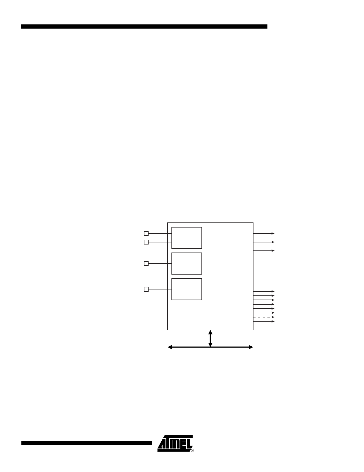
12. PMC: Power Management Controller
The AT91M42800A’s Power Management Controller optimizes the power consumption of the
device. The PMC controls the clocking elements such as the oscillator and the PLLs, and the
System and the Peripheral Clocks. It also controls the MCKO pin and enables the user to
select four different signals to be driven on this pin.
The AT91M42800A has the following clock elements:
• The oscillator, which provides a clock that depends on the crystal fundamental frequency
connected between the XIN and XOUT pins
• PLL A, which provides a low-to-middle frequency clock range
• PLL B, which provides a middle-to-high frequency range
• The Clock prescaler
• The System Clock controller
• The Peripheral Clock controller
• The Master Clock Output controller
The on-chip low-power oscillator together with the PLL-based frequency multiplier and the
prescaler results in a programmable clock between 500 Hz and 66 MHz. It is the responsibility
of the user to make sure that the PMC programming does not result in a clock over the acceptable limits.
AT91M42800A
Figure 12-1. Oscillator, PLL and Clock Sources
PLLRCA
PLLRCB
12.1 Oscillator and Slow Clock
The integrated oscillator generates the Slow Clock. It is designed for use with a 32.768 kHz
fundamental crystal. A 38.4 kHz crystal can be used. The bias resistor is on-chip and the oscillator integrates an equivalent load capacitance equal to 10 pF.
XIN
XOUT
32 kHz
Oscillator
PLLA
PLLB
Slow Clock (SLCK)
Main Clock (MCK)
ARM Core Clock
Power
Management
Controller
Peripheral
Clocks
User Interface
APB Bus
1779D–ATARM–14-Apr-06
55
Page 56
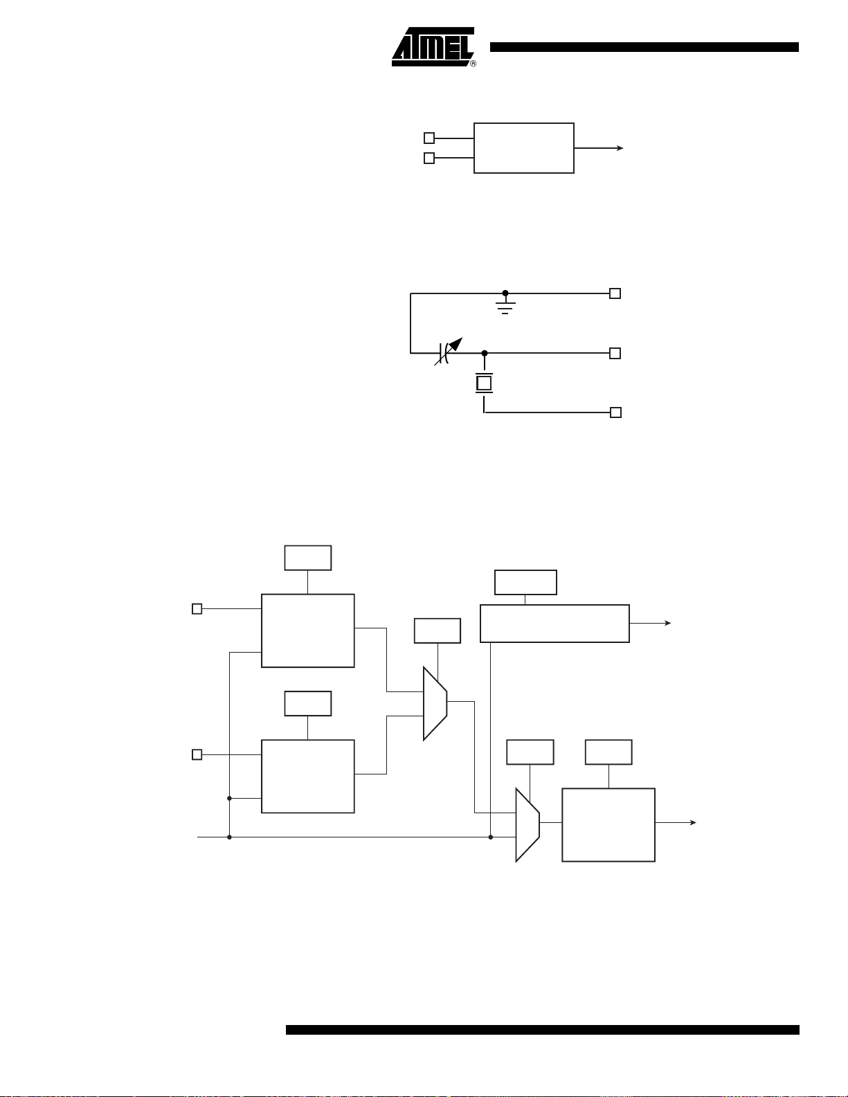
Figure 12-2. Slow Clock
12.2 Master Clock
Figure 12-4. Master Clock
XIN
XOUT SLCK
32 kHz
Oscillator
Slow Clock
To operate correctly, the crystal must be as close to the XIN and XOUT pins as possible. An
external variable capacitor can be added to adjust the oscillator frequency.
Figure 12-3. Crystal Location
GND
GROUND
PLANE
C
XIN
XOUT
The Master Clock (MCK) is generated from the Slow Clock by means of one of the two integrated PLLs and the prescaler.
PLLRCA
PLLRCB
SLCK
Slow Clock
Note: 1. Value written at reset and not subsequently programmable.
12.2.1 Phase Locked Loops
Two PLLs are integrated in the AT91M42800A in order to cover a larger frequency range.
Both PLLs have a Slow Clock input and a dedicated pin (PLLRCA or PLLRCB), which must
have appropriate capacitors and resistors. The capacitors and resistors serve as a second
MUL
PLLA
MUL
PLLB
PLLS
(1)
PLLCOUNT
Source
Clock
PLL Lock Timer
CSS PRES
Prescaler
Lock
MCK
Master Clock
56
AT91M42800A
1779D–ATARM–14-Apr-06
Page 57
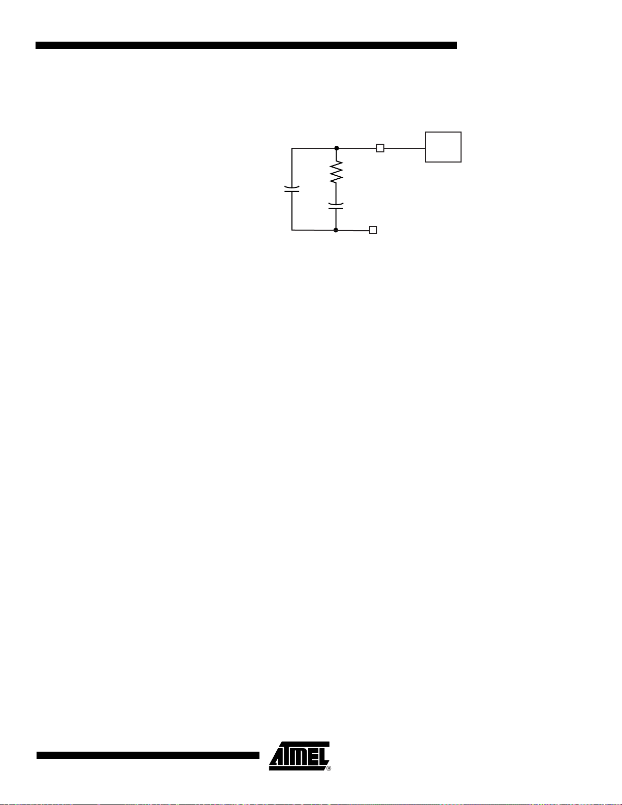
AT91M42800A
order filter. The PLLRC pin (A or B) that corresponds to the PLL that is disabled may be
grounded if capacitors and resistors need to be saved.
Figure 12-5. PLL Capacitors and Resistors
PLLRC
R
C2
C
GND
PLL
Typical values for the two PLLs are shown below:
PLLA:
F
= 32.768 kHz
SCLK
F
_PLLA = 16.776 MHz
out
R = 1600 Ohm
C = 100 nF
C
= 10 nF
2
With these parameters, the output frequency is stable (±10%) in 600 µs. This settling time is
the value to be programmed in the PLLCOUNT field of PMC_CGMR. The maximum frequency
overshoot during this phase is 22.5 MHz.
PLLB:
F
= 32.768 kHz
SCLK
F
_PLLB = 33.554 MHz
out
R = 800 Ohm
C = 1 µF
C
= 100 nF
2
With these parameters, the output frequency is stable (±10%) in 4 ms. This settling time is the
value to be programmed in the PLLCOUNT field of PMC_CGMR. The maximum frequency
overshoot during this phase is 38 MHz.
12.2.2 PLL Selection
The required PLL must be selected at the first writing access and cannot be changed after
that. The PLLS bit in PMC_CGMR (Clock Generator Mode Register) determines which PLL
module is activated. The other PLL is disabled in order to reduce power consumption and can
only be activated by another reset. Writing in PMC_CGMR with a different value has no effect.
12.2.3 Source Clock Selection
The bit CSS in PMC_CGMR selects the Slow Clock or the output of the activated PLL as the
Source Clock of the prescaler. After reset, the CSS field is 0, selecting the Slow Clock as
Source Clock.
When switching from Slow Clock to PLL Output, the Source Clock takes effect after 3 Slow
Clock cycles plus 2.5 PLL output signal cycles. This is a maximum value.
1779D–ATARM–14-Apr-06
57
Page 58

When switching from PLL Output to Slow Clock, the switch takes effect after 3.5 Slow Clock
cycles plus 2.5 PLL output signal cycles. This is a maximum value.
12.2.4 PLL Programming
Once the PLL is selected, the output of the active PLL is a multiple of the Slow Clock, determined by the MUL field of the PMC_CGMR. The value of the multiply factor can be up to 2048.
The multiplication factor is the programmed value plus one (MUL+1).
Each time PMC_CGMR is written with a MUL value different from the existing one, the LOCK
bit in PMC_SR is automatically cleared and the PLL Lock Timer is started (see Section 12.2.5
”PLL Lock Timer” on page 58). The LOCK bit is set when the PLL Lock Timer reaches 0.
If a null value is programmed in the MUL field, the PLL is automatically disabled and bypassed
to save power. The LOCK bit in PMC_SR is also automatically cleared.
The time during which the LOCK bit is cleared is user programmable in the field PLLCOUNT in
PMC_CGMR. The user must load this parameter with a value depending on the active PLL
and its start-up time or the frequency shift performed.
As long as the LOCK bit is 0, the PLL is automatically bypassed and its output is the Slow
Clock. This means:
• A switch from the PLL output to the Slow Clock and the associated delays, when the PLL is
locked.
• A switch from the Slow Clock to the PLL output and the associated delays, when the LOCK
bit is set.
12.2.5 PLL Lock Timer
The Power Management Controller of the AT91M42800A integrates a dedicated 8-bit timer for
the locking time of the PLL. This timer is loaded with the value written in PLLCOUNT each
time the value in the field MUL changes. At the same time, the LOCK bit in PMC_SR is
cleared, and the PLL is bypassed.
The timer counts down the value written in PLLCOUNT on the Slow Clock. The countdown
value ranges from 30 µs to 7.8 ms.
When the PLL Lock Timer reaches 0, the LOCK bit is set and can provide an interrupt.
The PLLCOUNT field is defined by the user, and depends on the current state of the PLL
(unlocked or locked), the targeted output frequency and the filter implemented on the PLLRC
pin.
12.2.6 Prescaler
The Clock Source (Slow Clock or PLL output) selected through the CSS field (Clock Source
Select) in PMC_CGMR can be divided by 1, 2, 4, 8, 16, 32 or 64. The default divider after a
reset is 1. The output of the prescaler is called Master Clock (MCK).
When the prescaler value is modified, the new defined Master Clock is effective after a maximum delay of 64 Source Clock cycles.
12.3 Master Clock Output Controller
The clock output on MCKO pin can be selected to be the Slow Clock, the Master Clock, the
Master Clock inverted or the Master Clock divided by two through the MCKOSS field (Master
Clock Output Source Select) in PMC_CGMR. The MCKO pad can be put in Tri-state mode to
58
AT91M42800A
1779D–ATARM–14-Apr-06
Page 59

AT91M42800A
save power consumption by setting the bit MCKODS (Master Clock Output Disable) in
PMC_CGMR. After a reset the MCKO pin is enabled and is driven by the Slow Clock.
Figure 12-6. Master Clock Output
MCKOSS
SLCK
Slow Clock
MCK
Master Clock
12.4 ARM Processor Clock Controller
The AT91M42800A has only one System Clock. It can be enabled and disabled by writing the
System Clock Enable (PMC_SCER) and System Clock Disable Registers (PMC_SCDR). The
status of this clock (at least for debug purpose) can be read in the System Clock Status Register (PMC_SCSR).
The system clock is enabled after a reset and is automatically re-enabled by any enabled
interrupt.
When the system clock is disabled, the current instruction is finished before the clock is
stopped.
Note: Stopping the ARM core does not prevent PDC transfers.
Figure 12-7. System Clock Control
MCKODS
MCKO
Master Clock Output
Divide by 2
12.5 Peripheral Clock Controller
The clock of each peripheral integrated in the AT91M42800A can be individually enabled and
disabled by writing into the Peripheral Clock Enable (PMC_PCER) and Peripheral Clock Disable (PMC_PCDR) registers. The status of the peripheral clock activity can be read in the
Peripheral Clock Status Register (PMC_PCSR).
1779D–ATARM–14-Apr-06
NIRQ
NFIQ
PMC_SCDR
Set
Idle
Mode
Register
Clear
PMC_SCSR
System
Clock
MCK
Master Clock
59
Page 60

When a peripheral clock is disabled, the clock is immediately stopped. When the clock is reenabled, the peripheral resumes action where it left off. The peripheral clocks are automatically disabled after a reset.
In order to stop a peripheral, it is recommended that the system software waits until the peripheral has executed its last programmed operation before disabling the clock. This is to avoid
data corruption or erroneous behavior of the system.
Note: The bits defined to control the Peripheral Clocks correspond to the bits controlling the Interrupt
Sources in the Interrupt Controller.
Figure 12-8. Peripheral Clock Control
MCK
Master Clock
Peripheral
Clock Y
PMC_PCER
PMC_PCDR
Set
PMC_PCSR
Clear
Peripheral
Clock X
YX
60
AT91M42800A
1779D–ATARM–14-Apr-06
Page 61

AT91M42800A
12.6 PMC User Interface
Base Address: 0xFFFF4000 (Code Label PMC_BASE)
Table 4. PMC Registers
Register
Offset Register Name
0x00 System Clock Enable Register PMC_SCER Write-only –
0x04 System Clock Disable Register PMC_SCDR Write-only –
0x08 System Clock Status Register PMC_SCSR Read-only 0x00000001
0x0C Reserved
0x10 Peripheral Clock Enable Register PMC_PCER Write-only –
0x14 Peripheral Clock Disable Register PMC_PCDR Write-only –
0x18 Peripheral Clock Status Register PMC_PCSR Read-only 0x00000000
0x1C Reserved
0x20 Clock Generator Mode Register PMC_CGMR Read/Write 0x00000000
0x24 Reserved
0x28 Reserved
0x2C Reserved
0x30 Status Register PMC_SR Read-only 0x00000000
0x34 Interrupt Enable Register PMC_IER Write-only –
Mnemonic Access Reset Value
––
––
––
––
––
–
–
–
–
–
0x38 Interrupt Disable Register PMC_IDR Write-only –
0x3C Interrupt Mask Register PMC_IMR Read-only 0x00000000
1779D–ATARM–14-Apr-06
61
Page 62

12.7 PMC System Clock Enable Register
Register Name: PMC_SCER
Access Type: Write-only
Offset: 0x00
31 30 29 28 27 26 25 24
––––––––
23 22 21 20 19 18 17 16
––––––––
15 14 13 12 11 10 9 8
––––––––
76543210
–––––––CPU
• CPU: System Clock Enable
0 = No effect.
1 = Enables the System Clock.
62
AT91M42800A
1779D–ATARM–14-Apr-06
Page 63

AT91M42800A
12.8 PMC System Clock Disable Register
Register Name: PMC_SCDR
Access Type: Write-only
Offset: 0x04
31 30 29 28 27 26 25 24
––––––––
23 22 21 20 19 18 17 16
––––––––
15 14 13 12 11 10 9 8
––––––––
76543210
–––––––CPU
• CPU: System Clock Disable
0 = No effect.
1 = Disables the System Clock.
12.9 PMC System Clock Status Register
Register Name: PMC_SCSR
Access Type: Read-only
Offset: 0x08
Reset Value: 0x01
31 30 29 28 27 26 25 24
––––––––
23 22 21 20 19 18 17 16
––––––––
15 14 13 12 11 10 9 8
––––––––
76543210
–––––––CPU
• CPU: System Clock Status
0 = System Clock is disabled.
1 = System Clock is enabled.
1779D–ATARM–14-Apr-06
63
Page 64

12.10 PMC Peripheral Clock Enable Register
Register Name: PMC_PCER
Access Type: Write-only
Offset: 0x10
31 30 29 28 27 26 25 24
–––––––––
23 22 21 20 19 18 17 16
––––––––
15 14 13 12 11 10 9 8
– PIOB PIOA – TC5 TC4 TC3 TC2
76543210
TC1 TC0 SPIB SPIA US1 US0 – –
• Peripheral Clock Enable
0 = No effect.
1 = Enables the peripheral clock.
12.11 PMC Peripheral Clock Disable Register
Register Name: PMC_PCDR
Access Type: Write-only
Offset: 0x14
31 30 29 28 27 26 25 24
––––––––
23 22 21 20 19 18 17 16
––––––––
15 14 13 12 11 10 9 8
– PIOB PIOA – TC5 TC4 TC3 TC2
76543210
TC1 TC0 SPIB SPIA US1 US0 – –
• Peripheral Clock Disable
0 = No effect.
1 = Disables the peripheral clock.
64
AT91M42800A
1779D–ATARM–14-Apr-06
Page 65

AT91M42800A
12.12 PMC Peripheral Clock Status Register
Register Name: PMC_PCSR
Access Type: Read-only
Offset: 0x1C
Reset Value: 0x0
31 30 29 28 27 26 25 24
––––––––
23 22 21 20 19 18 17 16
––––––––
15 14 13 12 11 10 9 8
– PIOB PIOA – TC5 TC4 TC3 TC2
76543210
TC1 TC0 SPIB SPIA US1 US0 – –
• Peripheral Clock Status
0 = Peripheral clock is disabled.
1 = Peripheral clock is enabled.
1779D–ATARM–14-Apr-06
65
Page 66

12.13 PMC Clock Generator Mode Register
Register Name: PMC_CGMR
Access Type: Read/Write
Offset: 0x20
Reset Value: 0x0
31 30 29 28 27 26 25 24
PLLCOUNT
23 22 21 20 19 18 17 16
––––– MUL
15 14 13 12 11 10 9 8
MUL
76543210
CSS MCKODS MCKOSS PLLS PRES
• PRES: Prescaler Selection
PRES Prescaler Selected Code Label PMC_PRES
0 0 0 None. The Prescaler is bypassed. PMC_PRES_NONE
001Divide by 2 PMC_PRES_DIV2
010Divide by 4 PMC_PRES_DIV4
011Divide by 8 PMC_PRES_DIV8
1 0 0 Divide by 16 PMC_PRES_DIV16
1 0 1 Divide by 32 PMC_PRES_DIV32
1 1 0 Divide by 64 PMC_PRES_DIV64
111Reserved –
• PLLS: PLL Selection
0 = The PLL A with 5 - 20 MHz output range is selected as PLL source. (Code Label PMC_PLL_A)
• 1 = The PLL B with 20 - 80 MHz output range is selected as PLL source. (Code Label PMC_PLL_B)
Note: This bit can be written only once after the reset. Any write of a different value than this one written the first time has no effect on
the bit.
• MCKOSS: Master Clock Output Source Selection
MCKOSS Master Clock Output Source Select Code Label: PMC_MCKOSS
0 0 Slow Clock PMC_MCKOSS_SLCK
0 1 Master Clock PMC_MCKOSS_MCK
1 0 Master Clock inverted PMC_MCKOSS_MCKINV
1 1 Master Clock divided by 2 PMC_MCKOSS_MCK_DIV2
• MCKODS: Master Clock Output Disable (Code Label PMC_MCKO_DIS)
0 = The pin MCKO is driven with the clock selected by MCKOSS.
1 = The pin MCKO is tri-stated.
66
AT91M42800A
1779D–ATARM–14-Apr-06
Page 67

AT91M42800A
• CSS: Clock Source Selection
0 = The clock source is the Slow Clock.
1 = The clock source is the output of the PLL.
• MUL: Phase Lock Loop Factor
0 = The PLL is disabled, reducing at the minimum its power consumption.
1 up to 2047 = The PLL output is at frequency (MUL+1) x Slow Clock frequency when the LOCK bit is set.
• PLLCOUNT: PLL Lock Counter
Specifies the number of 32,768 Hz clock cycles for the PLL lock timer to count before the PLL is locked, after the PLL is
started.
1779D–ATARM–14-Apr-06
67
Page 68

12.14 PMC Status Register
Register Name: PMC_SR
Access Type: Read-only
Offset: 0x30
Reset Value: 0x0
31 30 29 28 27 26 25 24
––––––––
23 22 21 20 19 18 17 16
––––––––
15 14 13 12 11 10 9 8
––––––––
76543210
–––––––LOCK
• LOCK: PLL Lock Status
0 = The PLL output signal is not stabilized.
1 = The PLL output signal is stabilized.
68
AT91M42800A
1779D–ATARM–14-Apr-06
Page 69

AT91M42800A
12.15 PMC Interrupt Enable Register
Register Name: PMC_IER
Access Type: Write-only
Offset: 0x34
31 30 29 28 27 26 25 24
––––––––
23 22 21 20 19 18 17 16
––––––––
15 14 13 12 11 10 9 8
––––––––
76543210
–––––––LOCK
• LOCK: PLL Lock Interrupt Enable
0 = No effect.
1 = Enables the PLL Lock Interrupt.
12.16 PMC Interrupt Disable Register
Register Name: PMC_IDR
Access Type: Write-only
Offset: 0x38
31 30 29 28 27 26 25 24
––––––––
23 22 21 20 19 18 17 16
––––––––
15 14 13 12 11 10 9 8
––––––––
76543210
–––––––LOCK
• LOCK: PLL Lock Interrupt Disable
0 = No effect.
1 = Disables the PLL Lock Interrupt.
1779D–ATARM–14-Apr-06
69
Page 70

12.17 PMC Interrupt Mask Register
Register Name: PMC_IMR
Access Type: Read-only
Offset: 0x3C
Reset Value: 0x0
31 30 29 28 27 26 25 24
––––––––
23 22 21 20 19 18 17 16
––––––––
15 14 13 12 11 10 9 8
––––––––
76543210
–––––––LOCK
• LOCK: PLL Lock Interrupt Mask
0 = The PLL Lock Interrupt is disabled.
1 = The PLL Lock Interrupt is enabled.
70
AT91M42800A
1779D–ATARM–14-Apr-06
Page 71
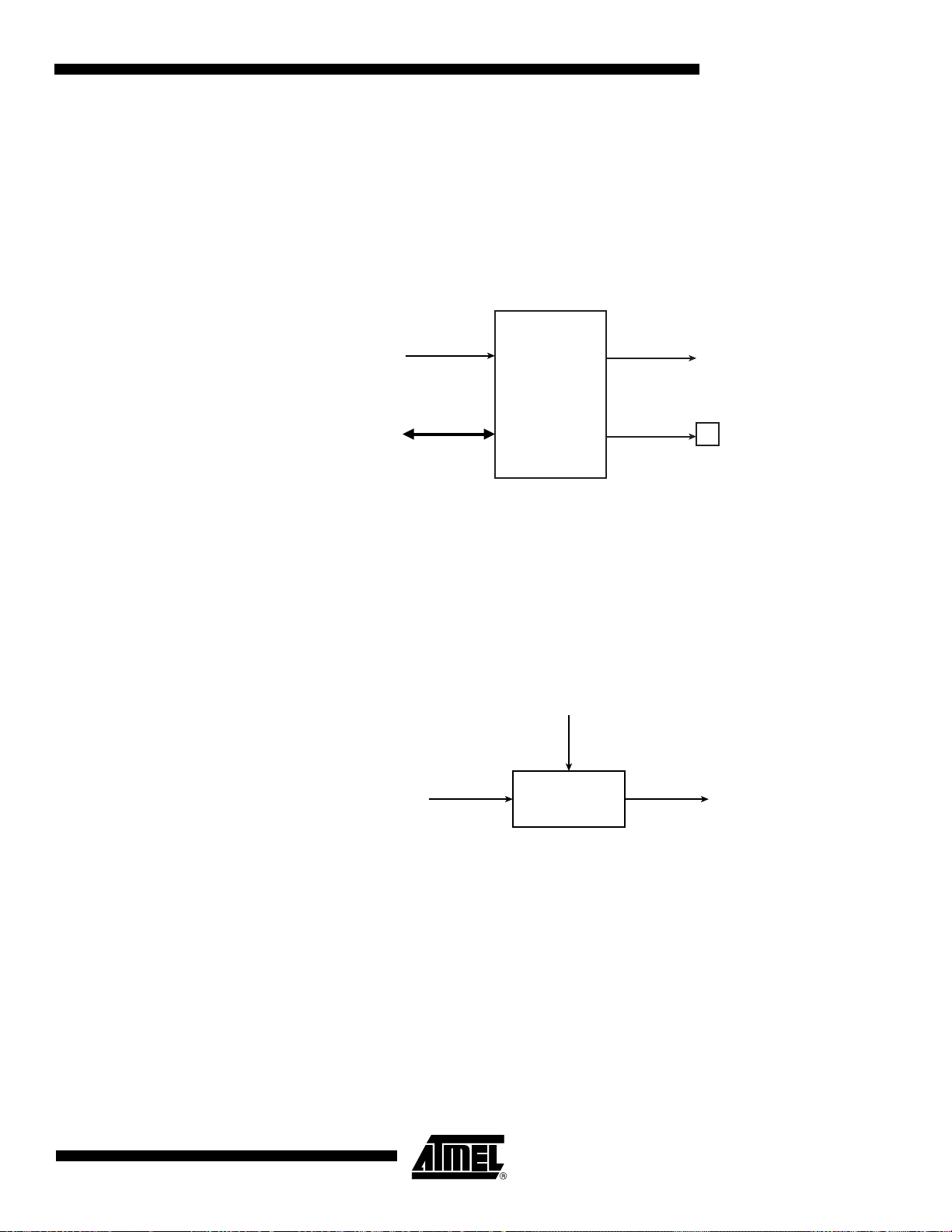
13. ST: System Timer
The System Timer module integrates three different free-running timers:
• A Period Interval Timer setting the base time for an Operating System.
• A Watchdog Timer having capabilities to reset the system in case of software deadlock.
• A Real-time Timer counting elapsed seconds.
These timers count using the Slow Clock. Typically, this clock has a frequency of 32.768 kHz.
Figure 13-1. System Timer Module
AT91M42800A
13.1 PIT: Period Interval Timer
The Period Interval Timer can be used to provide periodic interrupts for use by operating systems. It is built around a 16-bit down counter, which is preloaded by a value programmed in
ST_PIMR (Period Interval Mode Register). When the PIT counter reaches 0, the bit PITS is
set in ST_SR (Status Register), and an interrupt is generated, if it is enabled.
The counter is then automatically reloaded and restarted. Writing to the ST_PIMR at any time
immediately reloads and restarts the down counter with the new programmed value.
Figure 13-2. Period Interval Timer
SLCK
Slow Clock
APB
Interface
Slow Clock
SLCK
System
Timer
Module
PIV
Period Interval
Value
16-bit
Down Counter
STIRQ
System Timer Interrupt
NWDOVF
PITS
Period Interval
Timer Status
Note: If ST_PIMR is programmed with a period less or equal to the current MCK period, the update of
13.2 WDT: Watchdog Timer
The Watchdog Timer can be used to prevent system lock-up if the software becomes trapped
in a deadlock.
It is built around a 16-bit down counter loaded with the value defined in ST_WDMR (Watchdog
Mode Register). It uses the Slow Clock divided by 128. This allows the maximum watchdog
period to be 256 seconds (with a typical Slow Clock of 32.768 kHz).
In normal operation, the user reloads the watchdog at regular intervals before the timer overflow occurs. This is done by writing to the ST_CR (Control Register) with the bit WDRST set.
1779D–ATARM–14-Apr-06
the PITS status bit and its associated interrupt generation are unpredictable.
71
Page 72
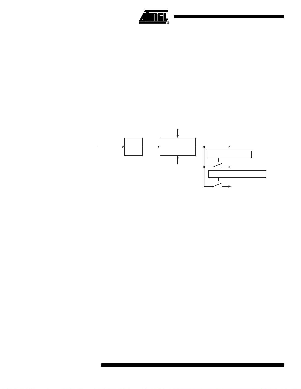
If an overflow does occur, the Watchdog Timer:
• Sets the WDOVF in ST_SR (Status Register) from which an interrupt can be generated
• Generates a pulse for 8 slow clock cycles on the external signal NWDOVF if the bit EXTEN
in ST_WDMR is set
• Generates an internal reset if the parameter RSTEN in ST_WDMR is set
• Reloads and restarts the down counter
Writing the ST_WDMR does not reload or restart the down counter. When the ST_CR is written the watchdog is immediately reloaded from ST_WDMR and restarted. The slow clock 128
divider is also immediately reset and restarted. When the ARM7TDMI enters debug mode, the
output of the slow clock divider stops, preventing any internal or external reset during the
debugging phase.
Figure 13-3. Watchdog Timer
WV
SLCK
Slow Clock
1/128
Watchdog Value
16-bit Down
Counter
RSTEN - Reset Enable
WDRST
Watchdog Restart
EXTEN- External Signal Enable
WDOVF
Watchdog Overflow
Internal Reset
13.3 RTT: Real-time Timer
The Real-time Timer can be used to count elapsed seconds. It is built around a 20-bit counter
fed by the Slow Clock divided by a programmable value. At reset this value is set to 0x8000,
corresponding to feeding the real-time counter with a 1 Hz signal when the Slow Clock is
32.768 Hz. The 20-bit counter can count up to 1048576 seconds, corresponding to more than
12 days, then roll over to 0.
The Real-time Timer value can be read at any time in the register ST_CRTR (Current Realtime Register). As this value can be updated asynchronously to the Master Clock, it is advisable to read this register twice at the same value to improve accuracy of the returned value.
This current value of the counter is compared with the value written in the Alarm Register
ST_RTAR (Real-time Alarm Register). If the counter value matches the alarm, the bit ALMS in
ST_SR is set. The Alarm Register is set to its maximum value, corresponding to 0, after a
reset.
The bit RTTINC in ST_SR is set each time the 20-bit counter is incremented. This bit can be
used to start an interrupt, or generate a one-second signal.
Writing the ST_RTMR immediately reloads and restarts the clock divider with the new programmed value. This also resets the 20-bit counter.
NWDOVF
72
AT91M42800A
1779D–ATARM–14-Apr-06
Page 73
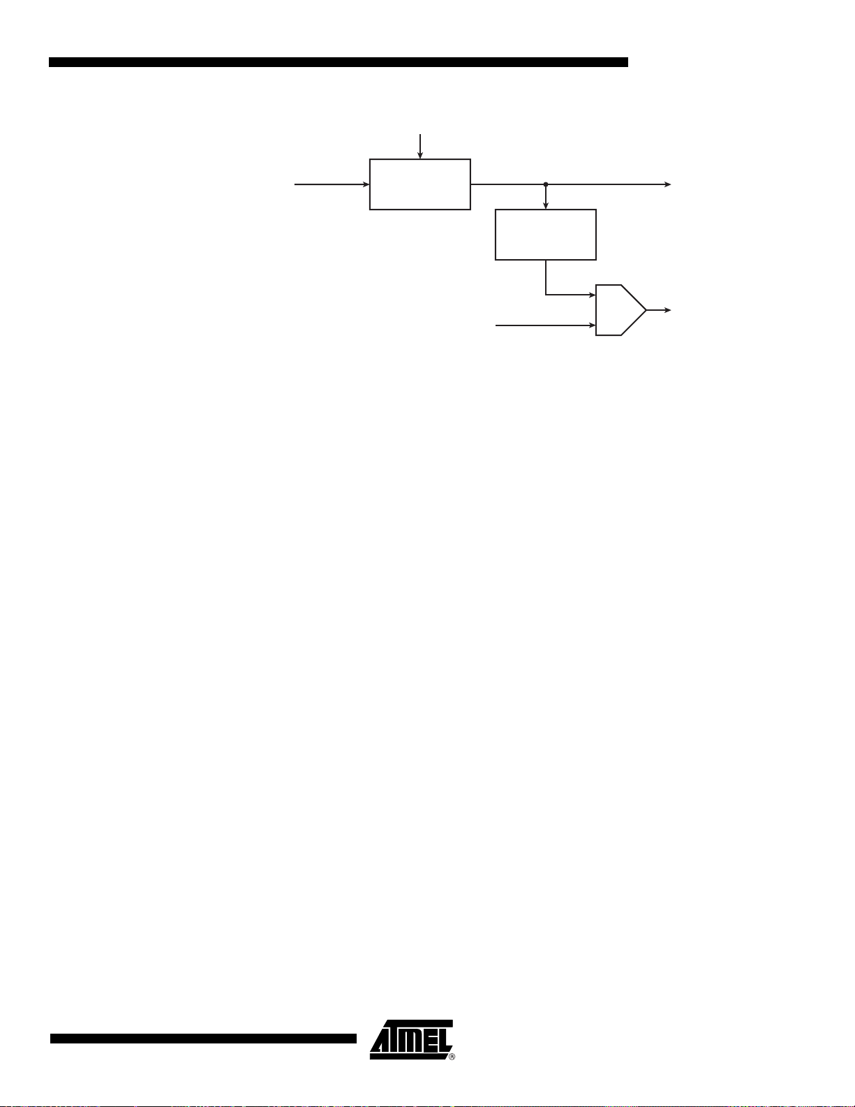
AT91M42800A
Figure 13-4. Real-time Timer
RTPRES
Real Time Prescalar
16-bit
SLCK
Slow Clock
Note: If RTPRES is programmed with a period less or equal to the current MCK period, the update of
the RTTINC and ALMS status bits and their associated interrupt generation are unpredictable.
Divider
20-bit
Counter
ALMV
Alarm Value
RTTINC
Real-time Timer
Increment
=
ALMS
Alarm Status
1779D–ATARM–14-Apr-06
73
Page 74

13.4 System Timer User Interface
System Timer Base Address: 0xFFFF8000
Table 5. System Timer Registers
Register
Offset Register Name
0x00 Control Register ST_CR W –
0x04 Period Interval Mode Register ST_PIMR R/W 0x00000000
0x08 Watchdog Mode Register ST_WDMR R/W 0x00020000
0x0C Real-time Mode Register ST_RTMR R/W 0x00008000
0x10 Status Register ST_SR R –
0x14 Interrupt Enable Register ST_IER W –
0x18 Interrupt Disable Register ST_IDR W –
0x1C Interrupt Mask Register ST_IMR R 0x0
0x20 Real-time Alarm Register ST_RTAR R/W 0x0
0x24 Current Real-time Register ST_CRTR R 0x0
Note: 1. Corresponds to maximum value of the counter.
Mnemonic Access Reset Value
13.5 System Timer Control Register
Register Name: ST_CR
Access Type: Write-only
Offset:
0x00
(1)
(1)
31 30 29 28 27 26 25 24
––––––––
23 22 21 20 19 18 17 16
––––––––
15 14 13 12 11 10 9 8
––––––––
76543210
–––––––WDRST
• WDRST: Watchdog Timer Restart
0 = No effect.
1 = Reload the start-up value in the Watchdog Timer.
74
AT91M42800A
1779D–ATARM–14-Apr-06
Page 75

AT91M42800A
13.6 System Timer Period Interval Mode Register
Register Name: ST_PIMR
Access Type: Read/Write
Offset:
Reset Value: 0x0
31 30 29 28 27 26 25 24
––––––––
23 22 21 20 19 18 17 16
––––––––
15 14 13 12 11 10 9 8
76543210
• PIV: Period Interval Value
Defines the value loaded in the 16-bit counter of the Period Interval Timer. The maximum period is obtained by programming PIV at 0x0 corresponding to 65536 Slow Clock cycles.
0x04
PIV
PIV
13.7 System Timer Watchdog Mode Register
Register Name: ST_WDMR
Access Type: Read/Write
Offset:
Reset Value: 0x0002 0000
31 30 29 28 27 26 25 24
––––––––
23 22 21 20 19 18 17 16
––––––EXTENRSTEN
15 14 13 12 11 10 9 8
76543210
• WDV: Watchdog Counter Value
Defines the value loaded in the 16-bit counter. The maximum period is obtained by programming WDV to 0x0 corresponding to 65536 • 128 Slow Clock cycles.
• RSTEN: Reset Enable
0 = No reset is generated when a watchdog overflow occurs.
1 = An internal reset is generated when a watchdog overflow occurs.
• EXTEN: External Signal Assertion Enable
0 = The NWDOVF is not tied low when a watchdog overflow occurs.
1 = The NWDOVF is tied low during 8 Slow Clock cycles when a watchdog overflow occurs.
0x08
WDV
WDV
1779D–ATARM–14-Apr-06
75
Page 76

13.8 System Timer Real-time Mode Register
Register Name: ST_RTMR
Access Type: Read/Write
Offset:
0x0C
Reset Value: 0x0000 8000
31 30 29 28 27 26 25 24
––––––––
23 22 21 20 19 18 17 16
––––––––
15 14 13 12 11 10 9 8
RTPRES
76543210
RTPRES
• RTPRES: Real-time Timer Prescaler Value
Defines the number of SLCK periods required to increment the Real-time Timer. The maximum period is obtained by programming RTPRES to 0x0 corresponding to 65536 Slow Clock cycles.
13.9 System Timer Status Register
Register Name: ST_SR
Access Type: Read-only
Offset:
0x10
31 30 29 28 27 26 25 24
––––––––
23 22 21 20 19 18 17 16
––––––––
15 14 13 12 11 10 9 8
––––––––
76543210
––––ALMSRTTINCWDOVFPITS
• PITS: Period Interval Timer Status
0 = The Period Interval Timer has not reached 0 since the last read of the Status Register.
1 = The Period Interval Timer has reached 0 since the last read of the Status Register.
• WDOVF: Watchdog Overflow
0 = The Watchdog Timer has not reached 0 since the last read of the Status Register.
1 = The Watchdog Timer has reached 0 since the last read of the Status Register.
• RTTINC: Real-time Timer Increment
0 = The Real-time Timer has not been incremented since the last read of the Status Register.
1 = The Real-time Timer has been incremented since the last read of the Status Register.
• ALMS: Alarm Status
0 = No alarm compare has been detected since the last read of the Status Register.
1 = Alarm compare has been detected since the last read of the Status Register.
76
AT91M42800A
1779D–ATARM–14-Apr-06
Page 77

AT91M42800A
13.10 System Timer Interrupt Enable Register
Register Name: ST_IER
Access Type: Write-only
Offset:
31 30 29 28 27 26 25 24
––––––––
23 22 21 20 19 18 17 16
––––––––
15 14 13 12 11 10 9 8
––––––––
76543210
––––ALMSRTTINCWDOVFPITS
• PITS: Period Interval Timer Status Interrupt Enable
0 = No effect.
1 = Enables the Period Interval Timer Status Interrupt.
• WDOVF: Watchdog Overflow Interrupt Enable
0 = No effect.
1 = Enables the Watchdog Overflow Interrupt.
• RTTINC: Real-time Timer Increment Interrupt Enable
0 = No effect.
1 = Enables the Real-time Timer Increment Interrupt.
• ALMS: Alarm Status Interrupt Enable
0 = No effect.
1 = Enables the Alarm Status Interrupt.
0x14
1779D–ATARM–14-Apr-06
77
Page 78

13.11 System Timer Interrupt Disable Register
Register Name: ST_IDR
Access Type: Write-only
Offset:
31 30 29 28 27 26 25 24
––––––––
23 22 21 20 19 18 17 16
––––––––
15 14 13 12 11 10 9 8
––––––––
76543210
––––ALMSRTTINCWDOVFPITS
• PITS: Period Interval Timer Status Interrupt Disable
0 = No effect.
1 = Disables the Period Interval Timer Status Interrupt.
• WDOVF: Watchdog Overflow Interrupt Disable
0 = No effect.
1 = Disables the Watchdog Overflow Interrupt.
• RTTINC: Real-time Timer Increment Interrupt Disable
0 = No effect.
1 = Disables the Real-time Timer Increment Interrupt.
• ALMS: Alarm Status Interrupt Disable
0 = No effect.
1 = Disables the Alarm Status Interrupt.
0x18
78
AT91M42800A
1779D–ATARM–14-Apr-06
Page 79

AT91M42800A
13.12 System Timer Interrupt Mask Register
Register Name: ST_IMR
Access Type: Read-only
Offset:
Reset Value: 0x0
31 30 29 28 27 26 25 24
––––––––
23 22 21 20 19 18 17 16
––––––––
15 14 13 12 11 10 9 8
––––––––
76543210
––––ALMSRTTINCWDOVFPITS
• PITS: Period Interval Timer Status Interrupt Mask
0 = Period Interval Timer Status Interrupt is disabled.
1 = Period Interval Timer Status Interrupt is enabled.
• WDOVF: Watchdog Overflow Interrupt Mask
0 = Watchdog Overflow Interrupt is disabled.
1 = Watchdog Overflow Interrupt is enabled.
• RTTINC: Real-time Timer Increment Interrupt Mask
0 = Real-time Timer Increment Interrupt is disabled.
1 = Real-time Timer Increment Interrupt is enabled.
• ALMS: Alarm Status Interrupt Mask
0 = Alarm Status Interrupt is disabled.
1 = Alarm Status Interrupt is enabled.
0x1C
1779D–ATARM–14-Apr-06
79
Page 80

13.13 System Timer Real-time Alarm Register
Register Name: ST_RTAR
Access Type: Read/Write
Offset:
0x20
Reset Value: 0x0
31 30 29 28 27 26 25 24
––––––––
23 22 21 20 19 18 17 16
ALMV
15 14 13 12 11 10 9 8
ALMV
76543210
ALMV
• ALMV: Alarm Value
Defines the Alarm value compared with the Real-time Timer. The maximum delay before ALMS status bit activation is
obtained by programming ALMV to 0x0 corresponding to 1048576 seconds.
13.14 System Timer Current Real-time Register
Register Name: ST_CRTR
Access Type: Read-only
Offset:
Reset Value: 0x0
0x24
31 30 29 28 27 26 25 24
––––––––
23 22 21 20 19 18 17 16
CRTV
15 14 13 12 11 10 9 8
CRTV
76543210
CRTV
• CRTV: Current Real-time Value
Returns the current value of the Real-time Timer.
80
AT91M42800A
1779D–ATARM–14-Apr-06
Page 81
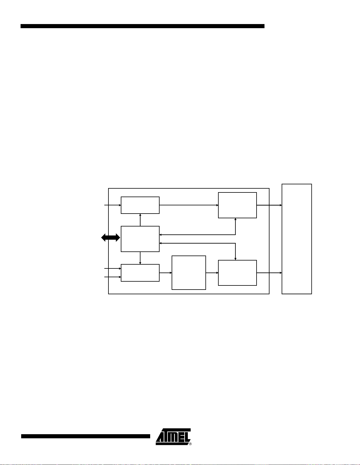
14. AIC: Advanced Interrupt Controller
The AT91M42800A has an 8-level priority, individually maskable, vectored interrupt controller.
This feature substantially reduces the software and real-time overhead in handling internal
and external interrupts.
The interrupt controller is connected to the NFIQ (fast interrupt request) and the NIRQ (standard interrupt request) inputs of the ARM7TDMI processor. The processor’s NFIQ line can
only be asserted by the external fast interrupt request input: FIQ. The NIRQ line can be
asserted by the interrupts generated by the on-chip peripherals and the external interrupt
request lines: IRQ0 to IRQ3.
The 8-level priority encoder allows the customer to define the priority between the different
NIRQ interrupt sources.
Internal sources are programmed to be level sensitive or edge triggered. External sources can
be programmed to be positive or negative edge triggered or high- or low-level sensitive.
The interrupt sources are listed in Table 14-1 and the AIC programmable registers in Table 6.
Figure 14-1. Interrupt Controller Block Diagram
AT91M42800A
FIQ Source
Advanced Peripheral
Bus (APB)
Internal Interrupt Sources
External Interrupt Sources
Memorization
Control
Logic
Memorization
Note: After a hardware reset, the external interrupt sources pins are controlled by the Controller. They
must be configured to be controlled by the peripheral before being used.
Prioritization
Controller
NFIQ
Manager
NIRQ
Manager
NFIQ
ARM7TDMI
Core
NIRQ
1779D–ATARM–14-Apr-06
81
Page 82

Table 14-1. AIC Interrupt Sources
Interrupt Source Interrupt Name Interrupt Description
0 FIQ Fast Interrupt
1 SW Soft Interrupt (generated by the AIC)
2 US0 USART Channel 0 interrupt
3 US1 USART Channel 1 interrupt
4 SPIA SPI Channel A Interrupt
5 SPIB SPI Channel B Interrupt
6 TC0 Timer Channel 0 Interrupt
7 TC1 Timer Channel 1 Interrupt
8 TC2 Timer Channel 2 Interrupt
9 TC3 Timer Channel 3 Interrupt
10 TC4 Timer Channel 4 Interrupt
11 TC5 Timer Channel 5 Interrupt
12 ST System Timer Interrupt
13 PIOA Parallel I/O Controller A Interrupt
14 PIOB Parallel I/O Controller B Interrupt
15 PMC Power Management Controller Interrupt
16 – Reserved
17 – Reserved
18 – Reserved
19 – Reserved
20 – Reserved
21 – Reserved
22 – Reserved
23 – Reserved
24 – Reserved
25 – Reserved
26 – Reserved
27 – Reserved
28 IRQ3 External Interrupt 3
29 IRQ2 External Interrupt 2
30 IRQ1 External Interrupt 1
31 IRQ0 External Interrupt 0
14.1 Hardware Interrupt Vectoring
The hardware interrupt vectoring reduces the number of instructions to reach the interrupt
handler to only one. By storing the following instruction at address 0x00000018, the processor
82
AT91M42800A
1779D–ATARM–14-Apr-06
Page 83

loads the program counter with the interrupt handler address stored in the AIC_IVR register.
Execution is then vectored to the interrupt handler corresponding to the current interrupt.
The current interrupt is the interrupt with the highest priority when the Interrupt Vector Register
(AIC_IVR) is read. The value read in the AIC_IVR corresponds to the address stored in the
Source Vector Register (AIC_SVR) of the current interrupt. Each interrupt source has its corresponding AIC_SVR. In order to take advantage of the hardware interrupt vectoring it is
necessary to store the address of each interrupt handler in the corresponding AIC_SVR, at
system initialization.
14.2 Priority Controller
The NIRQ line is controlled by an 8-level priority encoder. Each source has a programmable
priority level of 7 to 0. Level 7 is the highest priority and level 0 the lowest.
When the AIC receives more than one unmasked interrupt at a time, the interrupt with the
highest priority is serviced first. If both interrupts have equal priority, the interrupt with the lowest interrupt source number (see Table 14-1) is serviced first.
The current priority level is defined as the priority level of the current interrupt at the time the
register AIC_IVR is read (the interrupt which will be serviced).
AT91M42800A
ldr PC,[PC,# -&F20]
In the case when a higher priority unmasked interrupt occurs while an interrupt already exists,
there are two possible outcomes depending on whether the AIC_IVR has been read.
When the end of interrupt command register (AIC_EOICR) is written, the current interrupt level
is updated with the last stored interrupt level from the stack (if any). Hence at the end of a
higher priority interrupt, the AIC returns to the previous state corresponding to the preceding
lower priority interrupt which had been interrupted.
14.3 Interrupt Handling
The interrupt handler must read the AIC_IVR as soon as possible. This de-asserts the NIRQ
request to the processor and clears the interrupt in case it is programmed to be edge triggered. This permits the AIC to assert the NIRQ line again when a higher priority unmasked
interrupt occurs.
At the end of the interrupt service routine, the end of interrupt command register (AIC_EOICR)
must be written. This allows pending interrupts to be serviced.
• If the NIRQ line has been asserted but the AIC_IVR has not been read, then the processor
will read the new higher priority interrupt handler address in the AIC_IVR register and the
current interrupt level is updated.
• If the processor has already read the AIC_IVR then the NIRQ line is reasserted. When the
processor has authorized nested interrupts to occur and reads the AIC_IVR again, it reads
the new, higher priority interrupt handler address. At the same time the current priority
value is pushed onto a first-in last-out stack and the current priority is updated to the higher
priority.
14.4 Interrupt Masking
Each interrupt source, including FIQ, can be enabled or disabled using the command registers
AIC_IECR and AIC_IDCR. The interrupt mask can be read in the Read-only register AIC_IMR.
A disabled interrupt does not affect the servicing of other interrupts.
1779D–ATARM–14-Apr-06
83
Page 84

14.5 Interrupt Clearing and Setting
All interrupt sources which are programmed to be edge triggered (including FIQ) can be individually set or cleared by respectively writing to the registers AIC_ISCR and AIC_ICCR. This
function of the interrupt controller is available for auto-test or software debug purposes.
14.6 Fast Interrupt Request
The external FIQ line is the only source which can raise a fast interrupt request to the processor. Therefore, it has no priority controller.
The external FIQ line can be programmed to be positive or negative edge triggered or high- or
low-level sensitive in the AIC_SMR0 register.
The fast interrupt handler address can be stored in the AIC_SVR0 register. The value written
into this register is available by reading the AIC_FVR register when an FIQ interrupt is raised.
By storing the following instruction at address 0x0000001C, the processor will load the program counter with the interrupt handler address stored in the AIC_FVR register.
ldr PC,[PC,# -&F20]
Alternatively the interrupt handler can be stored starting from address 0x0000001C as
described in the ARM7TDMI datasheet.
14.7 Software Interrupt
Interrupt source 1 of the advanced interrupt controller is a software interrupt. It must be programmed to be edge triggered in order to set or clear it by writing to the AIC_ISCR and
AIC_ICCR.
This is totally independent of the SWI instruction of the ARM7TDMI processor.
14.8 Spurious Interrupt
When the AIC asserts the NIRQ line, the ARM7TDMI enters IRQ mode and the interrupt handler reads the IVR. It may happen that the AIC de-asserts the NIRQ line after the core has
taken into account the NIRQ assertion and before the read of the IVR.
This behavior is called a Spurious Interrupt.
The AIC is able to detect these Spurious Interrupts and returns the Spurious Vector when the
IVR is read. The Spurious Vector can be programmed by the user when the vector table is
initialized.
A spurious interrupt may occur in the following cases:
The same mechanism of spurious interrupt occurs if the ARM7TDMI reads the IVR (application software or ICE) when there is no interrupt pending. This mechanism is also valid for the
FIQ interrupts.
Once the AIC enters the spurious interrupt management, it asserts neither the NIRQ nor the
NFIQ lines to the ARM7TDMI as long as the spurious interrupt is not acknowledged. Therefore, it is mandatory for the Spurious Interrupt Service Routine to acknowledge the “spurious”
• With any sources programmed to be level sensitive, if the interrupt signal of the AIC input is
de-asserted at the same time as it is taken into account by the ARM7TDMI.
• If an interrupt is asserted at the same time as the software is disabling the corresponding
source through AIC_IDCR (this can happen due to the pipelining of the ARM core).
84
AT91M42800A
1779D–ATARM–14-Apr-06
Page 85

14.9 Protect Mode
AT91M42800A
behavior by writing to the AIC_EOICR (End of Interrupt) before returning to the interrupted
software. It also can perform other operation(s), e.g., trace possible undesirable behavior.
The Protect Mode permits reading of the Interrupt Vector Register without performing the
associated automatic operations. This is necessary when working with a debug system.
When a Debug Monitor or an ICE reads the AIC User Interface, the IVR could be read. This
would have the following consequences in normal mode.
• If an enabled interrupt with a higher priority than the current one is pending, it is stacked.
• If there is no enabled pending interrupt, the spurious vector is returned.
In either case, an End of Interrupt command would be necessary to acknowledge and to
restore the context of the AIC. This operation is generally not performed by the debug system.
Hence the debug system would become strongly intrusive, and could cause the application to
enter an undesired state.
This is avoided by using Protect mode.
The Protect mode is enabled by setting the AIC bit in the SF Protect Mode Register (see ”SF:
Special Function Registers” on page 115).
When Protect mode is enabled, the AIC performs interrupt stacking only when a write access
is performed on the AIC_IVR. Therefore, the Interrupt Service Routines must write (arbitrary
data) to the AIC_IVR just after reading it.
The new context of the AIC, including the value of the Interrupt Status Register (AIC_ISR), is
updated with the current interrupt only when IVR is written.
An AIC_IVR read on its own (e.g., by a debugger), modifies neither the AIC context nor the
AIC_ISR.
Extra AIC_IVR reads performed in between the read and the write can cause unpredictable
results. Therefore, it is strongly recommended not to set a breakpoint between these two
actions, nor to stop the software.
The debug system must not write to the AIC_IVR as this would cause undesirable effects.
The following table shows the main steps of an interrupt and the order in which they are performed according to the mode:
Action Normal Mode Protect Mode
Calculate active interrupt (higher than current or spurious) Read AIC_IVR Read AIC_IVR
Determine and return the vector of the active interrupt Read AIC_IVR Read AIC_IVR
Memorize interrupt Read AIC_IVR Read AIC_IVR
Push on internal stack the current priority level Read AIC_IVR Write AIC_IVR
Acknowledge the interrupt
No effect
(2)
(1)
Notes: 1. NIRQ de-assertion and automatic interrupt clearing if the source is programmed as level
sensitive.
2. Software that has been written and debugged using Protect mode will run correctly in Normal mode without modification. However, in Normal mode, the AIC_IVR write has no effect
and can be removed to optimize the code.
Read AIC_IVR Write AIC_IVR
Write AIC_IVR –
1779D–ATARM–14-Apr-06
85
Page 86

14.10 AIC User Interface
Base Address: 0xFFFFF000 (Code Label AIC_BASE)
Table 6. AIC Memory Map
Offset Register Name Access Reset State
0x000 Source Mode Register 0 AIC_SMR0 Read/Write 0
0x004 Source Mode Register 1 AIC_SMR1 Read/Write 0
– – – Read/Write 0
0x07C Source Mode Register 31 AIC_SMR31 Read/Write 0
0x080 Source Vector Register 0 AIC_SVR0 Read/Write 0
0x084 Source Vector Register 1 AIC_SVR1 Read/Write 0
– – – Read/Write 0
0x0FC Source Vector Register 31 AIC_SVR31 Read/Write 0
0x100 IRQ Vector Register AIC_IVR Read-only –
0x104 FIQ Vector Register AIC_FVR Read-only –
0x108 Interrupt Status Register AIC_ISR Read-only –
0x10C Interrupt Pending Register AIC_IPR Read-only (see
0x110 Interrupt Mask Register AIC_IMR Read-only 0
0x114 Core Interrupt Status Register AIC_CISR Read-only –
0x118 Reserved – – –
(1)
)
0x11C Reserved – – –
0x120 Interrupt Enable Command Register AIC_IECR Write-only –
0x124 Interrupt Disable Command Register AIC_IDCR Write-only –
0x128 Interrupt Clear Command Register AIC_ICCR Write-only –
0x12C Interrupt Set Command Register AIC_ISCR Write-only –
0x130 End of Interrupt Command Register AIC_EOICR Write-only –
0x134 Spurious Vector Register AIC_SPU Read/Write 0
Note: 1. The reset value of this register depends on the level of the External IRQ lines. All other
sources are cleared at reset.
86
AT91M42800A
1779D–ATARM–14-Apr-06
Page 87

AT91M42800A
14.11 AIC Source Mode Register
Register Name: AIC_SMR0..AIC_SMR31
Access Type: Read/Write
Reset Value: 0
31 30 29 28 27 26 25 24
––––––––
23 22 21 20 19 18 17 16
––––––––
15 14 13 12 11 10 9 8
––––––––
76543210
– SRCTYPE – – PRIOR
• PRIOR: Priority Level (Code Label AIC_PRIOR)
Program the priority level for all sources except source 0 (FIQ).
The priority level can be between 0 (lowest) and 7 (highest).
The priority level is not used for the FIQ, in the SMR0.
• SRCTYPE: Interrupt Source Type (Code Label AIC_SRCTYPE)
Program the input to be positive or negative edge-triggered or positive or negative level sensitive.
The active level or edge is not programmable for the internal sources.
SRCTYPE External Sources Code Label
0 0 Low-level Sensitive AIC_SRCTYPE_EXT_LOW_LEVEL
0 1 Negative Edge triggered AIC_SRCTYPE_EXT_NEGATIVE_EDGE
1 0 High-level Sensitive AIC_SRCTYPE_EXT_HIGH_LEVEL
1 1 Positive Edge triggered AIC_SRCTYPE_EXT_POSITIVE_EDGE
SRCTYPE Internal Sources Code Label
X 0 Level Sensitive AIC_SRCTYPE_INT_LEVEL_SENSITIVE
X 1 Edge triggered AIC_SRCTYPE_INT_EDGE_TRIGGERED
1779D–ATARM–14-Apr-06
87
Page 88

14.12 AIC Source Vector Register
Register Name: AIC_SVR0..AIC_SVR31
Access Type: Read/Write
Reset Value: 0
31 30 29 28 27 26 25 24
VECTOR
23 22 21 20 19 18 17 16
VECTOR
15 14 13 12 11 10 9 8
VECTOR
76543210
VECTOR
• VECTOR: Interrupt Handler Address
The user may store in these registers the addresses of the corresponding handler for each interrupt source.
14.13 AIC Interrupt Vector Register
Register Name: AIC_IVR
Access Type: Read-only
Offset:
31 30 29 28 27 26 25 24
0x100
IRQV
23 22 21 20 19 18 17 16
IRQV
15 14 13 12 11 10 9 8
IRQV
76543210
IRQV
• IRQV: Interrupt Vector Register
The IRQ Vector Register contains the vector programmed by the user in the Source Vector Register corresponding to the
current interrupt.
The Source Vector Register (1 to 31) is indexed using the current interrupt number when the Interrupt Vector Register is
read.
When there is no current interrupt, the IRQ Vector Register reads the value stored in AIC_SPU.
88
AT91M42800A
1779D–ATARM–14-Apr-06
Page 89

AT91M42800A
14.14 AIC FIQ Vector Register
Register Name: AIC_FVR
Access Type: Read-only
Offset:
31 30 29 28 27 26 25 24
23 22 21 20 19 18 17 16
15 14 13 12 11 10 9 8
76543210
• FIQV: FIQ Vector Register
The FIQ Vector Register contains the vector programmed by the user in the Source Vector Register 0 which corresponds
to FIQ.
14.15 AIC Interrupt Status Register
Register Name: AIC_ISR
Access Type: Read-only
Offset:
0x104
FIQV
FIQV
FIQV
FIQV
0x108
31 30 29 28 27 26 25 24
–––––––––
23 22 21 20 19 18 17 16
––––––––
15 14 13 12 11 10 9 8
––––––––
76543210
––– IRQID
• IRQID: Current IRQ Identifier (Code Label AIC_IRQID)
The Interrupt Status Register returns the current interrupt source number.
1779D–ATARM–14-Apr-06
89
Page 90

14.16 AIC Interrupt Pending Register
Register Name: AIC_IPR
Access Type: Read-only
Offset:
31 30 29 28 27 26 25 24
IRQ0 IRQ1 IRQ2 IRQ3 – – – –
23 22 21 20 19 18 17 16
––––––––
15 14 13 12 11 10 9 8
PMC PIOB PIOA ST TC5 TC4 TC3 TC2
76543210
TC1 TC0 SPIB SPIA US1 US0 SW FIQ
0x10C
• Interrupt Pending
0 = Corresponding interrupt is inactive.
1 = Corresponding interrupt is pending.
14.17 AIC Interrupt Mask Register
Register Name: AIC_IMR
Access Type: Read-only
Offset:
Reset Value: 0x0
0x110
31 30 29 28 27 26 25 24
IRQ0 IRQ1 IRQ2 IRQ3 – – – –
23 22 21 20 19 18 17 16
––––––––
15 14 13 12 11 10 9 8
PMC PIOB PIOA ST TC5 TC4 TC3 TC2
76543210
TC1 TC0 SPIB SPIA US1 US0 SW FIQ
• Interrupt Mask
0 = Corresponding interrupt is disabled.
1 = Corresponding interrupt is enabled.
90
AT91M42800A
1779D–ATARM–14-Apr-06
Page 91

AT91M42800A
14.18 AIC Core Interrupt Status Register
Register Name: AIC_CISR
Access Type: Read-only
Offset:
31 30 29 28 27 26 25 24
––––––––
23 22 21 20 19 18 17 16
––––––––
15 14 13 12 11 10 9 8
––––––––
76543210
––––––NIRQNFIQ
• NFIQ: NFIQ Status (Code Label AIC_NFIQ)
0 = NFIQ line inactive.
1 = NFIQ line active.
• NIRQ: NIRQ Status (Code Label AIC_NIRQ)
0 = NIRQ line inactive.
1 = NIRQ line active.
0x114
1779D–ATARM–14-Apr-06
91
Page 92

14.19 AIC Interrupt Enable Command Register
Register Name: AIC_IECR
Access Type: Write-only
Offset:
31 30 29 28 27 26 25 24
IRQ0 IRQ1 IRQ2 IRQ3 – – – –
23 22 21 20 19 18 17 16
––––––––
15 14 13 12 11 10 9 8
PMC PIOB PIOA ST TC5 TC4 TC3 TC2
76543210
TC1 TC0 SPIB SPIA US1 US0 SW FIQ
0x120
• Interrupt Enable
0 = No effect.
1 = Enables corresponding interrupt.
14.20 AIC Interrupt Disable Command Register
Register Name: AIC_IDCR
Access Type: Write-only
Offset:
0x124
31 30 29 28 27 26 25 24
IRQ0 IRQ1 IRQ2 IRQ3 – – – –
23 22 21 20 19 18 17 16
––––––––
15 14 13 12 11 10 9 8
PMC PIOB PIOA ST TC5 TC4 TC3 TC2
76543210
TC1 TC0 SPIB SPIA US1 US0 SW FIQ
• Interrupt Disable
0 = No effect.
1 = Disables corresponding interrupt.
92
AT91M42800A
1779D–ATARM–14-Apr-06
Page 93

AT91M42800A
14.21 AIC Interrupt Clear Command Register
Register Name: AIC_ICCR
Access Type: Write-only
Offset:
31 30 29 28 27 26 25 24
IRQ0 IRQ1 IRQ2 IRQ3 – – – –
23 22 21 20 19 18 17 16
––––––––
15 14 13 12 11 10 9 8
PMC PIOB PIOA ST TC5 TC4 TC3 TC2
76543210
TC1 TC0 SPIB SPIA US1 US0 SW FIQ
• Interrupt Clear
0 = No effect.
1 = Clears corresponding interrupt.
14.22 AIC Interrupt Set Command Register
Register Name: AIC_ISCR
Access Type: Write-only
Offset:
0x128
0x12C
31 30 29 28 27 26 25 24
IRQ0 IRQ1 IRQ2 IRQ3 – – – –
23 22 21 20 19 18 17 16
––––––––
15 14 13 12 11 10 9 8
PMC PIOB PIOA ST TC5 TC4 TC3 TC2
76543210
TC1 TC0 SPIB SPIA US1 US0 SW FIQ
• Interrupt Set
0 = No effect.
1 = Sets corresponding interrupt.
1779D–ATARM–14-Apr-06
93
Page 94

14.23 AIC End of Interrupt Command Register
Register Name: AIC_EOICR
Access Type: Write-only
Offset:
31 30 29 28 27 26 25 24
––––––––
23 22 21 20 19 18 17 16
–––––
15 14 13 12 11 10 9 8
–––––––
76543210
––––––––
0x130
–––
–
The End of Interrupt Command Register is used by the interrupt routine to indicate that the interrupt treatment is complete.
Any value can be written because it is only necessary to make a write to this register location to signal the end of interrupt
treatment.
14.24 AIC Spurious Vector Register
Register Name: AIC_SPU
Access Type: Read/Write
Offset:
Reset Value: 0
0x134
31 30 29 28 27 26 25 24
SPUVEC
23 22 21 20 19 18 17 16
SPUVEC
15 14 13 12 11 10 9 8
SPUVEC
76543210
SPUVEC
• SPUVEC: Spurious Interrupt Vector Handler Address
The user may store the address of the spurious interrupt handler in this register.
94
AT91M42800A
1779D–ATARM–14-Apr-06
Page 95

14.25 Standard Interrupt Sequence
It is assumed that:
• The Advanced Interrupt Controller has been programmed, AIC_SVR are loaded with
corresponding interrupt service routine addresses and interrupts are enabled.
• The Instruction at address 0x18(IRQ exception vector address) is
ldr pc, [pc, #-&F20]
When NIRQ is asserted, if the bit I of CPSR is 0, the sequence is:
1. The CPSR is stored in SPSR_irq, the current value of the Program Counter is loaded
in the IRQ link register (R14_irq) and the Program Counter (R15) is loaded with 0x18.
In the following cycle during fetch at address 0x1C, the ARM core adjusts R14_irq,
decrementing it by 4.
2. The ARM core enters IRQ mode, if it is not already.
3. When the instruction loaded at address 0x18 is executed, the Program Counter is
loaded with the value read in AIC_IVR. Reading the AIC_IVR has the following
effects:
– Set the current interrupt to be the pending one with the highest priority. The current
level is the priority level of the current interrupt.
– De-assert the NIRQ line on the processor. (Even if vectoring is not used, AIC_IVR
must be read in order to de-assert NIRQ)
– Automatically clear the interrupt, if it has been programmed to be edge triggered.
– Push the current level on to the stack.
– Return the value written in the AIC_SVR corresponding to the current interrupt.
4. The previous step has effect to branch to the corresponding interrupt service routine.
This should start by saving the Link Register(R14_irq) and the SPSR(SPSR_irq).
Note that the Link Register must be decremented by 4 when it is saved, if it is to be
restored directly into the Program Counter at the end of the interrupt.
5. Further interrupts can then be unmasked by clearing the I-bit in the CPSR, allowing
re-assertion of the NIRQ to be taken into account by the core. This can occur if an
interrupt with a higher priority than the current one occurs.
6. The Interrupt Handler can then proceed as required, saving the registers which will
be used and restoring them at the end. During this phase, an interrupt of priority
higher than the current level will restart the sequence from step 1. Note that if the
interrupt is programmed to be level sensitive, the source of the interrupt must be
cleared during this phase.
7. The I-bit in the CPSR must be set in order to mask interrupts before exiting, to ensure
that the interrupt is completed in an orderly manner.
8. The End of Interrupt Command Register (AIC_EOICR) must be written in order to
indicate to the AIC that the current interrupt is finished. This causes the current level
to be popped from the stack, restoring the previous current level if one exists on the
stack. If another interrupt is pending, with lower or equal priority than old current level
but with higher priority than the new current level, the NIRQ line is re-asserted, but
the interrupt sequence does not immediately start because the I-bit is set in the core.
AT91M42800A
1779D–ATARM–14-Apr-06
95
Page 96

9. The SPSR (SPSR_irq) is restored. Finally, the saved value of the Link Register is
restored directly into the PC. This has effect of returning from the interrupt to whatever was being executed before, and of loading the CPSR with the stored SPSR,
masking or unmasking the interrupts depending on the state saved in the SPSR (the
previous state of the ARM core).
Note: The I-bit in the SPSR is significant. If it is set, it indicates that the ARM core was just about to
mask IRQ interrupts when the mask instruction was interrupted. Hence, when the SPSR is
restored, the mask instruction is completed (IRQ is masked).
14.26 Fast Interrupt Sequence
It is assumed that:
• The Advanced Interrupt Controller has been programmed, AIC_SVR[0] is loaded with fast
interrupt service routine address and the fast interrupt is enabled.
• The Instruction at address 0x1C(FIQ exception vector address) is:
ldr pc, [pc, #-&F20]
• Nested Fast Interrupts are not needed by the user.
When NFIQ is asserted, if the F-bit of CPSR is 0, the sequence is:
1. The CPSR is stored in SPSR_fiq, the current value of the Program Counter is loaded
in the FIQ link register (R14_fiq) and the Program Counter (R15) is loaded with 0x1C.
In the following cycle, during fetch at address 0x20, the ARM core adjusts R14_fiq,
decrementing it by 4.
2. The ARM core enters FIQ mode.
3. When the instruction loaded at address 0x1C is executed, the Program Counter is
loaded with the value read in AIC_FVR. Reading the AIC_FVR has effect of automatically clearing the fast interrupt (source 0 connected to the FIQ line), if it has been
programmed to be edge triggered. In this case only, it de-asserts the NFIQ line on the
processor.
4. The previous step has effect to branch to the corresponding interrupt service routine.
It is not necessary to save the Link Register(R14_fiq) and the SPSR(SPSR_fiq) if
nested fast interrupts are not needed.
5. The Interrupt Handler can then proceed as required. It is not necessary to save registers R8 to R13 because FIQ mode has its own dedicated registers and the user R8 to
R13 are banked. The other registers, R0 to R7, must be saved before being used,
and restored at the end (before the next step). Note that if the fast interrupt is programmed to be level sensitive, the source of the interrupt must be cleared during this
phase in order to de-assert the NFIQ line.
6. Finally, the Link Register (R14_fiq) is restored into the PC after decrementing it by 4
(with instruction sub pc, lr, #4 for example). This has effect of returning from the interrupt to whatever was being executed before, and of loading the CPSR with the SPSR,
masking or unmasking the fast interrupt depending on the state saved in the SPSR.
Note: The F-bit in the SPSR is significant. If it is set, it indicates that the ARM core was just about to
mask FIQ interrupts when the mask instruction was interrupted. Hence when the SPSR is
restored, the interrupted instruction is completed (FIQ is masked).
96
AT91M42800A
1779D–ATARM–14-Apr-06
Page 97

15. PIO: Parallel I/O Controller
The AT91M42800A has 54 programmable I/O lines. I/O lines are multiplexed with an external
signal of a peripheral to optimize the use of available package pins (see Tables Table 15-1 on
page 100 and Table 15-2 on page 101). These lines are controlled by two separate and identi-
cal PIO Controllers called PIOA and PIOB. Each PIO controller also provides an internal
interrupt signal to the Advanced Interrupt Controller.
Note: After a hardware reset, the PIO clock is disabled by default (see Section 12. ”PMC: Power Man-
agement Controller” on page 55). The user must configure the Power Management Controller
before any access to the User Interface of the PIO.
15.1 Multiplexed I/O Lines
When a peripheral signal is not used in an application, the corresponding pin can be used as a
parallel I/O. Each parallel I/O line is bi-directional, whether the peripheral defines the signal as
input or output. Figure 15-1 shows the multiplexing of the peripheral signals with Parallel I/O
signals.
A pin is controlled by the registers PIO_PER (PIO Enable) and PIO_PDR (PIO Disable). The
register PIO_PSR (PIO Status) indicates whether the pin is controlled by the corresponding
peripheral or by the PIO Controller.
When the PIO is selected, the peripheral input line is connected to zero.
AT91M42800A
15.2 Output Selection
15.3 I/O Levels
15.4 Filters
The user can enable each individual I/O signal as an output with the registers PIO_OER (Output Enable) and PIO_ODR (Output Disable). The output status of the I/O signals can be read
in the register PIO_OSR (Output Status). The direction defined has effect only if the pin is configured to be controlled by the PIO Controller.
Each pin can be configured to be driven high or low. The level is defined in four different ways,
according to the following conditions.
• If a pin is controlled by the PIO Controller and is defined as an output (see Section 15.2
”Output Selection” on page 97 above), the level is programmed using the registers
PIO_SODR (Set Output Data) and PIO_CODR (Clear Output Data). In this case, the
programmed value can be read in PIO_ODSR (Output Data Status).
• If a pin is controlled by the PIO Controller and is not defined as an output, the level is
determined by the external circuit.
• If a pin is not controlled by the PIO Controller, the state of the pin is defined by the
peripheral (see peripheral datasheets).
In all cases, the level on the pin can be read in the register PIO_PDSR (Pin Data Status).
Optional input glitch filtering is available on each pin and is controlled by the registers
PIO_IFER (Input Filter Enable) and PIO_IFDR (Input Filter Disable). The input glitch filtering
can be selected whether the pin is used for its peripheral function or as a parallel I/O line. The
register PIO_IFSR (Input Filter Status) indicates whether or not the filter is activated for each
pin.
1779D–ATARM–14-Apr-06
97
Page 98

15.5 Interrupts
Each parallel I/O can be programmed to generate an interrupt when a level change occurs.
This is controlled by the PIO_IER (Interrupt Enable) and PIO_IDR (Interrupt Disable) registers
which enable/disable the I/O interrupt by setting/clearing the corresponding bit in the
PIO_IMR. When a change in level occurs, the corresponding bit in the PIO_ISR (Interrupt Status) is set whether the pin is used as a PIO or a peripheral and whether it is defined as input or
output. If the corresponding interrupt in PIO_IMR (Interrupt Mask) is enabled, the PIO interrupt
is asserted.
When PIO_ISR is read, the register is automatically cleared.
15.6 User Interface
Each individual I/O is associated with a bit position in the Parallel I/O user interface registers.
Each of these registers are 32 bits wide. If a parallel I/O line is not defined, writing to the corresponding bits has no effect. Undefined bits read zero.
15.7 Multi-driver (Open Drain)
Each I/O can be programmed for multi-driver option. This means that the I/O is configured as
open drain (can only drive a low level) in order to support external drivers on the same pin. An
external pull-up is necessary to guarantee a logic level of one when the pin is not being driven.
Registers PIO_MDER (Multi-Driver Enable) and PIO_MDDR (Multi-Driver Disable) control this
option. Multi-driver can be selected whether the I/O pin is controlled by the PIO Controller or
the peripheral. PIO_MDSR (Multi-Driver Status) indicates which pins are configured to support
external drivers.
98
AT91M42800A
1779D–ATARM–14-Apr-06
Page 99
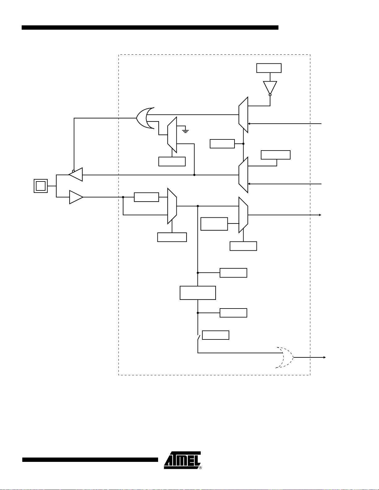
Figure 15-1. Parallel I/O Multiplexed with a Bi-directional Signal
Pad Output Enable
0
1
0
AT91M42800A
PIO_OSR
Peripheral
Output
Enable
Pad
Pad Output
Pad Input
Filter
1
PIO_MDSR
1
0
PIO_IFSR
Event
Detection
PIO_PSR
OFF
Value
(1)
PIO_PSR
PIO_PDSR
PIO_ISR
PIO_ODSR
1
0
0
1
Peripheral
Output
Peripheral
Input
1779D–ATARM–14-Apr-06
PIO_IMR
PIOIRQ
Note: 1. See Section 15.8 ”PIO Connection Tables” on page 100.
99
Page 100

15.8 PIO Connection Tables
Table 15-1. PIO Controller A Connection Table
PIO Controller Peripheral
Bit
Number
0 PA0 IRQ0 External Interrupt 0 Input 0 PIO Input 77
1 PA1 IRQ1 External Interrupt 1 Input 0 PIO Input 78
2 PA2 IRQ2 External Interrupt 2 Input 0 PIO Input 79
3 PA3 IRQ3 External Interrupt 3 Input 0 PIO Input 80
4 PA4 FIQ Fast Interrupt Input 0 PIO Input 81
5 PA5 SCK0 USART0 Clock Signal Bi-directional 0 PIO Input 82
6 PA6 TXD0 USART0 Transmit Data Signal Output – PIO Input 83
7 PA7 RXD0 USART0 Receive Data Signal Input 0 PIO Input 86
8 PA8 SCK1 USART1 Clock Signal Bi-directional 0 PIO Input 87
9 PA9 TXD1/NTRI USART1 Transmit Data Signal Output – PIO Input 88
10 PA10 RXD1 USART1 Receive Data Signal Input 0 PIO Input 89
11 PA11 SPCKA SPIA Clock Signal Bi-directional 0 PIO Input 90
12 PA12 MISOA SPIA Master In Slave Out Bi-directional 0 PIO Input 91
13 PA13 MOSIA SPIA Master Out Slave In Bi-directional 0 PIO Input 92
Port
Name Port Name Signal Description
Signal
Direction
OFF
Value
(1)
Reset State
Pin
Number
14 PA14 NPCSA0/NSSA SPIA Peripheral Chip Select 0 Bi-directional 1 PIO Input 93
15 PA15 NPCSA1 SPIA Peripheral Chip Select 1 Output – PIO Input 94
16 PA16 NPCSA2 SPIA Peripheral Chip Select 2 Output – PIO Input 95
17 PA17 NPCSA3 SPIA Peripheral Chip Select 3 Output – PIO Input 98
18 PA18 SPCKB SPIB Clock Signal Bi-directional 0 PIO Input 99
19 PA19 MISOB SPIB Master In Slave Out Bi-directional 0 PIO Input 100
20 PA20 MOSIB SPIB Master Out Slave In Bi-directional 0 PIO Input 101
21 PA21 NPCSB0/NSSB SPIB Peripheral Chip Select 0 Bi-directional 1 PIO Input 102
22 PA22 NPCSB1 SPIB Peripheral Chip Select 1 Output – PIO Input 103
23 PA23 NPCSB2 SPIB Peripheral Chip Select 2 Output – PIO Input 104
24 PA24 NPCSB3 SPIB Peripheral Chip Select 3 Output – PIO Input 105
25 PA25 MCKO Master Clock Output Output – MCKO 106
26 PA26 – – – – PIO Input 111
27 PA27 BMS Boot Mode Select Input 0 PIO Input 123
28 PA28 – – Output – PIO Input 131
29 PA29 PME Protect Mode Enable Input 0 PIO Input 134
Note: 1. The OFF value is the default level seen on the peripheral input when the PIO line is enabled.
100
AT91M42800A
1779D–ATARM–14-Apr-06
 Loading...