


BDTIC www.bdtic.com/ATMEL
Features
• Incorporates the ARM7TDMI
– High-performance 32-bit RISC Architecture
– High-density 16-bit Instruction Set
– Leader in MIPS/Watt
– Embedded ICE (In-circuit Emulation)
• 256K Bytes of On-chip SRAM
– 32-bit Data Bus, Single-clock Cycle Access
• 1024K Words 16-bit Flash Memory (2M bytes)
– Single Voltage Read/Write,
– Sector Erase Architecture
– Erase Suspend Capability
– Low-power Operation
– Data Polling, Toggle Bit and Ready/Busy End of Program Cycle Detection
– Reset Input for Device Initialization
– Sector Program Unlock Command
– 128-bit Protection Register
– Factory-programmed AT91 Flash Memory Uploader Software
• Fully Programmable External Bus Interface (EBI)
– Up to 8 Chip Selects, Maximum External Address Space of 64M Bytes
– Software Programmable 8/16-bit External Data Bus
• 8-level Priority, Individually Maskable, Vectored Interrupt Controller
– 4 External Interrupts, Including a High-priority Low-latency Interrupt Request
• 32 Programmable I/O Lines
• 3-channel 16-bit Timer/Counter
– 3 External Clock Inputs, 2 Multi-purpose I/O Pins per Channel
• 2 USARTs
– 2 Dedicated Peripheral Data Controller (PDC) Channels per USART
• Programmable Watchdog Timer
• Advanced Power-saving Features
– CPU and Peripherals Can be De-activated Individually
• Fully Static Operation:
– 0 Hz to 75 MHz Internal Frequency Range at VDDCORE = 1.8V, 85°C
• 2.7V to 3.6V I/O Operating Range, 1.65V to 1.95V Core Operating Range
• -40°C to 85° C Temperature Range
• Available in a 121-ball 10 x 10 x 1.2 mm BGA Package with 0.8 mm Ball Pitch
®
ARM® Thumb® Processor Core
AT91 ARM®
Thumb
®
Microcontrollers
AT91FR40162S
Summary
Preliminary
1. Description
The AT91FR40162S is a member of the Atmel AT91 16/32-bit Microcontroller family,
which is based on the ARM7TDMI processor core. The processor has a high-performance 32-bit RISC architecture with a high-density 16-bit instruction set and very low
power consumption.
The AT91FR40162S ARM microcontroller features 2 Mbits of on-chip SRAM and 2
Mbytes of Flash memory in a single compact 121-ball BGA package. Its high level of
integration and very small footprint make the device ideal for space-constrained applications. The high-speed on-chip SRAM enables a performance of up to 74 MIPs in
typical conditions with significant power reduction and EMC improvement over an
external SRAM implementation.
The Flash memory may be programmed via the JTAG/ICE interface or the factoryprogrammed Flash Memory Uploader (FMU) using a single device supply, making the
AT91FR40162S suitable for in-system programmable applications.
6174AS–ATARM–25-May-05
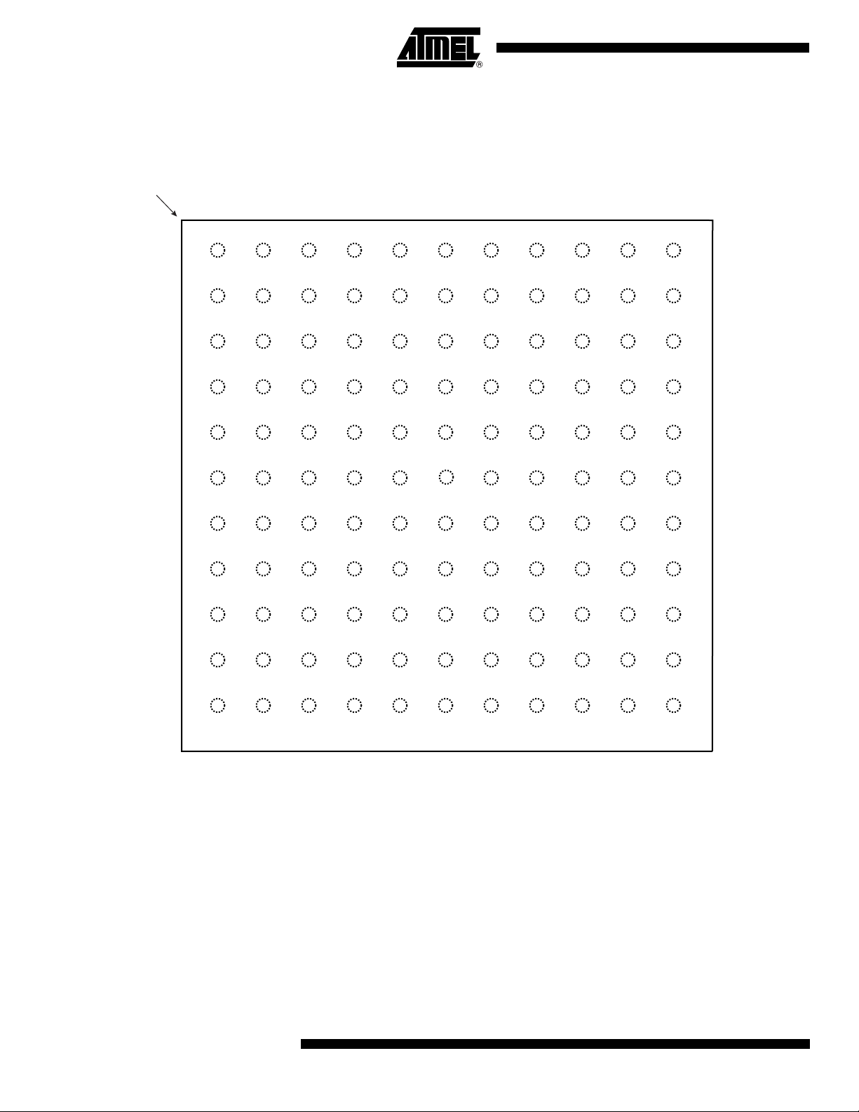
2. Pin Configuration
Figure 2-1. AT91FR40162S Pinout for 121-ball BGA Package (Top View)
A1 Corner
1110987654321
P21/TXD1
NTRI
P22
RXD1
VDDIO
P23
P24
BMS
GND
TDO
P26
NCS2
NWAIT
NCS1
GND
P19 P16 GND
P20
SCK1
GND
MCKI NRST
P25
MCK0
TMS GND TCK D8 NC NC
NWE
NWR0
VDDCORE VDDIO NC
GND
NLB
A0
A1 A4 A6 VDDIO A18
P15
RXD0
P18 P17
NUB
NWR1
NWDOVF A3 NC NC D3
A2 TDI D6 GND NC
P27
NCS3
GND A7 A17
P14
TXD0
P13
SCK0
A5 A19 VDDIO
P12
FIQ
NBUSY P9
VPP NRSTF A14 A15
A8 D11 D10 D13
NOE
NRD
NCS0 D2 D5 D4
NCSF NC D0 D1
NC VDDIO GND GND
VDDIO A10 A13 GND
VDDIO A9 A12 GND
P11
VDDCORE
IRQ2
P10
VDDIO
IRQ1
IRQ0P5TIOB1P3TCLK1
D9
A11 D7
P8
TIOB2P6TCLK2
P7
TIOA2P4TIOA1
GND
GND
A16
D12 D14 VDDIO
P31/A23
CS4
D15
NC NC
P29/A21
CS6
P30/A22
VDDCORE
P2
TIOB0
P1
TIOA0
P0
TCLK0
CS5
A20
A
B
C
D
E
F
G
H
J
K
L
2
AT91FR40162S
6174AS–ATARM–25-May-05

3. Pin Description
Table 3-1. AT91FR40162S Pin Description
Module Name Function Type
AT91FR40162S
Active
Level Comments
EBI
AIC
Timer
A0 - A23 Address Bus Output –
D0 - D15 Data Bus I/O –
NCS0 - NCS3 External Chip Select Output Low Used to select external devices
CS4 - CS7 External Chip Select Output High A23 - A20 after reset
NWR0 Lower Byte 0 Write Signal Output Low Used in Byte Write option
NWR1 Upper Byte 1 Write Signal Output Low Used in Byte Write option
NRD Read Signal Output Low Used in Byte Write option
NWE Write Enable Output Low Used in Byte Select option
NOE Output Enable Output Low Used in Byte Select option
NUB Upper Byte Select Output Low Used in Byte Select option
NLB Lower Byte Select Output Low Used in Byte Select option
NWAIT Wait Input Input Low
BMS Boot Mode Select Input –
FIQ Fast Interrupt Request Input – PIO-controlled after reset
IRQ0 - IRQ2 External Interrupt Request Input – PIO-controlled after reset
TCLK0 - TCLK2 Timer External Clock Input – PIO-controlled after reset
TIOA0 - TIOA2 Multi-purpose Timer I/O Pin A I/O – PIO-controlled after reset
Valid after reset; do not reprogram A20 to
I/O, as it is MSB of Flash address
Sampled during reset; must be driven low
during reset for Flash to be used as boot
memory
TIOB0 - TIOB2 Multi-purpose Timer I/O Pin B I/O – PIO-controlled after reset
SCK0 - SCK1 External Serial Clock I/O – PIO-controlled after reset
USART
PIO P0 - P31 Parallel IO Line I/O –
WD NWDOVF Watchdog Overflow Output Low Open drain
Clock
Reset
ICE
6174AS–ATARM–25-May-05
TXD0 - TXD1 Transmit Data Output Output – PIO-controlled after reset
RXD0 - RXD1 Receive Data Input Input – PIO-controlled after reset
MCKI Master Clock Input Input – Schmidt trigger
MCKO Master Clock Output Output –
NRST Hardware Reset Input Input Low Schmidt trigger
NTRI Tri-state Mode Select Input Low Sampled during reset
TMS Test Mode Select Input – Schmidt trigger, internal pull-up
TDI Test Data Input Input – Schmidt trigger, internal pull-up
TDO Test Data Output Output –
TCK Test Clock Input – Schmidt trigger, internal pull-up
3

Table 3-1. AT91FR40162S Pin Description (Continued)
Module Name Function Type
NCSF Flash Memory Select Input Low Enables
Flash
Memory
NBUSY Flash Memory Busy Output Output Low Flash RDY/BUSY
NRSTF Flash Memory Reset Input Input Low Resets Flash to standard operating mode
Active
Level Comments
Flash Memory when pulled low
signal; open-drain
Power
VDDIO Power Power –
VDDCORE Power Power –
GND Ground Ground –
VPP Write Protection Input Low
All V
DDIO, VDDCORE
MUST be connected to their respective
supplies by the shortest route
Provides data protection (Program/Erase)
when VPP input is below 0.4V
and all GND pins
4
AT91FR40162S
6174AS–ATARM–25-May-05
4. Block Diagram
Figure 4-1. AT91FR40162S
D0-D15
A1- A19
A0/NLB
A20
NWR1/NUB
NWAIT
NCS0
NCS1
NRD/NOE
NWR0/NWE
P26/NCS2
P27/NCS3
P29/A21/CS6
P30/A22/CS5
P31/A23/CS4
GND
VPP
VDDIO
VDDIO
NRSTF
NCSF
NBUSY
P0/TCLK0
P3/TCLK1
P6/TCLK2
P1/TIOA0
AT91FR40162S
P2/TIOB0
P4/TIOA1
P5/TIOB1
P7/TIOA2
P8/TIOB2
D0 - D15
ASB
A0/NLB
A1 - A19
P28/A20/NCS7
VPP
VCC
GND
OE WE
A0 - A18
D0 - D15
A19
FLASH MEMORY
EBI: External Bus Interface
Interface
EBI User
AMBA Bridge
MCU
APB
CE
BYTE
RESET
RDY/BUSY
I
P
O
AT91R40008
TC0
Counter
TC: Timer
TC1
TC2
6174AS–ATARM–25-May-05
ARM7TDMI Core
ICE
Embedded
TDI
TCK
TMS
TDO
SRAM
256K Bytes
GND
VDDIO
VDDCORE
Reset
NRST
ASB
Controller
Clock
MCKI
P25/MCKO
AIC: Advanced
Interrupt Controller
P12/FIQ
P9/IRQ0
P10/IRQ1
P11/IRQ2
2 PDC
Channels
USART0
P14/TXD0
P13/SCK0
P15/RXD0
2 PDC
Channels
USART1
I
P
O
P16
P20/SCK1
P22/RXD1
P21/TXD1/NTRI
Chip ID
PS: Power Saving
P17
P18
P19
P23
P24/BMS
PIO: Parallel I/O Controller
WD: Watchdog Timer
NWDOVF
5

5. Architectural Overview
The AT91FR40162S integrates Atmel’s AT91R40008 ARM Thumb processor and a 2-Mbyte
(16-Mbit) Flash memory die in a single compact 121-ball BGA package. The address, data
and control signals, except the Flash memory enable, are internally interconnected.
The AT91R40008 architecture consists of two main buses, the Advanced System Bus (ASB)
and the Advanced Peripheral Bus (APB). Designed for maximum performance and controlled
by the memory controller, the ASB interfaces the ARM7TDMI processor with the on-chip 32-bit
SRAM memory, the External Bus Interface (EBI) connected to the encapsulated Flash and the
™
AMBA
peripherals and optimized for low power consumption.
The AT91FR40162S implements the ICE port of the ARM7TDMI processor on dedicated pins,
offering a complete, low-cost and easy-to-use debug solution for target debugging.
5.1 Memories
The AT91FR40162S embeds 256K bytes of internal SRAM. The internal memory is directly
connected to the 32-bit data bus and is single-cycle accessible. This provides maximum performance of 67 MIPS at 75 MHz by using the ARM instruction set of the processor, minimizing
system power consumption and improving on the performance of separate memory solutions.
The AT91FR40162S features an External Bus Interface (EBI), which enables connection of
external memories and application-specific peripherals. The EBI supports 8- or 16-bit devices
and can use two 8-bit devices to emulate a single 16-bit device. The EBI implements the early
read protocol, enabling faster memory accesses than standard memory interfaces.
Bridge. The AMBA Bridge drives the APB, which is designed for accesses to on-chip
5.2 Peripherals
The AT91FR40162S encapsulates a Flash memory organized as 1024K 16-bit words,
accessed via the EBI. A 16-bit Thumb instruction can be loaded from Flash memory in a single
access. Separate MCU and Flash memory reset inputs (NRST and NRSTF) are provided for
maximum flexibility. The user is thus free to tailor the reset operation to the application.
The AT91FR40162S integrates resident boot software called AT91 Flash Memory Uploader
software in the encapsulated Flash. The AT91 Flash Memory Uploader software is able to
upload program application software into its Flash memory.
The AT91FR40162S integrates several peripherals, which are classified as system or user
peripherals.
All on-chip peripherals are 32-bit accessible by the AMBA Bridge, and can be programmed
with a minimum number of instructions. The peripheral register set is composed of control,
mode, data, status and enable/disable/status registers.
An on-chip Peripheral Data Controller (PDC) transfers data between the on-chip USARTs and
on- and off-chip memory address space without processor intervention. Most importantly, the
PDC removes the processor interrupt handling overhead, making it possible to transfer up to
64K contiguous bytes without reprogramming the start address, thus increasing the performance of the microcontroller, and reducing the power consumption.
6
AT91FR40162S
6174AS–ATARM–25-May-05

5.2.1 System Peripherals
The External Bus Interface (EBI) controls the external memory or peripheral devices via an 8or 16-bit databus and is programmed through the APB. Each chip select line has its own programming register.
The Power-saving (PS) module implements the Idle Mode (ARM7TDMI core clock stopped
until the next interrupt) and enables the user to adapt the power consumption of the microcontroller to application requirements (independent peripheral clock control).
The Advanced Interrupt Controller (AIC) controls the internal interrupt sources from the internal peripherals and the four external interrupt lines (including the FIQ) to provide an interrupt
and/or fast interrupt request to the ARM7TDMI. It integrates an 8-level priority controller, and,
using the Auto-vectoring feature, reduces the interrupt latency time.
The Parallel Input/Output Controller (PIO) controls up to 32 I/O lines. It enables the user to
select specific pins for on-chip peripheral input/output functions, and general-purpose
input/output signal pins. The PIO controller can be programmed to detect an interrupt on a signal change from each line.
The Watchdog (WD) can be used to prevent system lock-up if the software becomes trapped
in a deadlock.
The Special Function (SF) module integrates the Chip ID, the Reset Status and the Protect
registers.
AT91FR40162S
5.2.2 User Peripherals
Two USARTs, independently configurable, enable communication at a high baud rate in synchronous or asynchronous mode. The format includes start, stop and parity bits and up to 8
data bits. Each USART also features a Timeout and a Time Guard register, facilitating the use
of the two dedicated Peripheral Data Controller (PDC) channels.
The 3-channel, 16-bit Timer Counter (TC) is highly programmable and supports capture or
waveform modes. Each TC channel can be programmed to measure or generate different
kinds of waves, and can detect and control two input/output signals. The TC has also 3 external clock signals.
6174AS–ATARM–25-May-05
7

6. Product Overview
6.1 Power Supply
The AT91FR40162S device has two types of power supply pins:
• VDDCORE pins that power the chip core (i.e., the AT91R40008 with its embedded SRAM
and peripherals)
• VDDIO pins that power the AT91R40008 I/O lines and the Flash memory
An independent I/O supply allows a flexible adaptation to external component signal levels.
6.2 Input/Output Considerations
The AT91FR40162S I/O pads accept voltage levels up to the VDDIO power supply limit. After
the reset, the microcontroller peripheral I/Os are initialized as inputs to provide the user with
maximum flexibility. It is recommended that in any application phase, the inputs to the microcontroller be held at valid logic levels to minimize the power consumption.
6.3 Master Clock
The AT91FR40162S has a fully static design and works on the Master Clock (MCK), provided
on the MCKI pin from an external source.
The Master Clock is also provided as an output of the device on the pin MCKO, which is multiplexed with a general purpose I/O line. While NRST is active, and after the reset, the MCKO is
valid and outputs an image of the MCK signal. The PIO Controller must be programmed to use
this pin as standard I/O line.
6.4 Reset
Reset restores the default states of the user interface registers (defined in the user interface of
each peripheral), and forces the ARM7TDMI to perform the next instruction fetch from address
zero. Except for the program counter the ARM7TDMI registers do not have defined reset
states.
6.4.1 NRST Pin
NRST is an active low-level input. It is asserted asynchronously, but exit from reset is synchronized internally to the MCK. The signal presented on MCKI must be active within the
specification for a minimum of 10 clock cycles up to the rising edge of NRST to ensure correct
operation. The first processor fetch occurs 80 clock cycles after the rising edge of NRST.
6.4.2 Watchdog Reset
The watchdog can be programmed to generate an internal reset. In this case, the reset has
the same effect as the NRST pin assertion, but the pins BMS and NTRI are not sampled. Boot
Mode and Tri-state Mode are not updated. If the NRST pin is asserted and the watchdog triggers the internal reset, the NRST pin has priority.
6.5 Emulation Functions
6.5.1 Tri-state Mode
The AT91FR40162S microcontroller provides a tri-state mode, which is used for debug purposes. This enables the connection of an emulator probe to an application board without
8
AT91FR40162S
6174AS–ATARM–25-May-05

having to desolder the device from the target board. In tri-state mode, all the output pin drivers
of the AT91R40008 microcontroller are disabled.
In tri-state mode, direct access to the Flash via external pins is provided. This enables production Flash programming using classical Flash programmers prior to board mounting.
To enter tri-state mode, the NTRI pin must be held low during the last 10 clock cycles before
the rising edge of NRST. For normal operation, the NTRI pin must be held high during reset by
a resistor of up to 400 kΩ.
NTRI is multiplexed with I/O line P21 and USART1 serial data transmit line TXD1.
6.5.2 JTAG/ICE Debug
ARM-standard embedded In-circuit Emulation is supported via the JTAG/ICE port. The pins
TDI, TDO, TCK and TMS are dedicated to this debug function and can be connected to a host
computer via the external ICE interface. In ICE Debug Mode, the ARM7TDMI core responds
with a non-JTAG chip ID that identifies the microcontroller. This is not fully IEEE1149.1
compliant.
6.6 Memory Controller
The ARM7TDMI processor address space is 4G bytes. The memory controller decodes the
internal 32-bit address bus and defines three address spaces:
AT91FR40162S
6.6.1 Internal Memories
• Internal memories in the four lowest megabytes
• Middle space reserved for the external devices (memory or peripherals) controlled by the
EBI
• Internal peripherals in the four highest megabytes
In any of these address spaces, the ARM7TDMI operates in little-endian mode only.
The AT91FR40162S microcontroller integrates 256K bytes of internal SRAM. It is 32 bits wide
and single-clock cycle accessible. Byte (8-bit), half-word (16-bit) and word (32-bit) accesses
are supported and are executed within one cycle. Fetching either Thumb or ARM instructions
is supported, and internal memory can store two times as many Thumb instructions as ARM
instructions.
The SRAM is mapped at address 0x0 (after the Remap command), allowing ARM7TDMI
exception vectors between 0x0 and 0x20 to be modified by the software.
Placing the SRAM on-chip and using the 32-bit data bus bandwidth maximizes the microcontroller performance and minimizes system power consumption. The 32-bit bus increases the
effectiveness of the use of the ARM instruction set and the processing of data that is wider
than 16 bits, thus making optimal use of the ARM7TDMI advanced performance.
Being able to dynamically update application software in the 256-Kbyte SRAM adds an extra
dimension to the AT91FR40162S.
6174AS–ATARM–25-May-05
The AT91FR40162S also integrates a 2-Mbyte Flash memory that is accessed via the External Bus Interface. All data, address and control lines, except for the Chip Select signal, are
connected within the device.
9

6.6.2 Boot Mode Select
6.6.3 Remap Command
The ARM reset vector is at address 0x0. After the NRST line is released, the ARM7TDMI executes the instruction stored at this address. This means that this address must be mapped in
nonvolatile memory after the reset. The input level on the BMS pin during the last 10 clock
cycles before the rising edge of the NRST selects the type of boot memory (see Table 3-1 on
page 3).
If the embedded Flash memory is to be used as boot memory, the BMS input must be pulled
down externally and NCS0 must be connected to NCSF externally.
The pin BMS is multiplexed with the I/O line P24 that can be programmed after reset like any
standard PIO line.
Table 6-1. Boot Mode Select
BMS Boot Memory
1 External 8-bit memory on NCS0
0 Internal or External 16-bit memory on NCS0
The ARM vectors (Reset, Abort, Data Abort, Prefetch Abort, Undefined Instruction, Interrupt,
Fast Interrupt) are mapped from address 0x0 to address 0x20. In order to allow these vectors
to be redefined dynamically by the software, the AT91FR40162S uses a remap command that
enables switching between the boot memory and the internal primary SRAM bank addresses.
The remap command is accessible through the EBI User Interface by writing one in RCB of
EBI_RCR (Remap Control Register). Performing a remap command is mandatory if access to
the other external devices (connected to chip selects 1 to 7) is required. The remap operation
can only be changed back by an internal reset or an NRST assertion.
6.6.4 Abort Control
The abort signal providing a Data Abort or a Prefetch Abort exception to the ARM7TDMI is
asserted when accessing an undefined address in the EBI address space.
No abort is generated when reading the internal memory or by accessing the internal peripherals, whether the address is defined or not.
6.6.5 External Bus Interface
The External Bus Interface handles the accesses between addresses 0x0040 0000 and
0xFFC0 0000. It generates the signals that control access to the external devices, and can be
configured from eight 1-Mbyte banks up to four 16-Mbyte banks. It supports byte, half-word
and word aligned accesses.
For each of these banks, the user can program:
• Number of wait states
• Number of data float times (wait time after the access is finished to prevent any bus
contention in case the device is too long in releasing the bus)
• Data bus width (8-bit or 16-bit)
• With a 16-bit wide data bus, the user can program the EBI to control one 16-bit device
(Byte Access Select Mode) or two 8-bit devices in parallel that emulate a 16-bit memory
(Byte Write Access Mode).
10
AT91FR40162S
6174AS–ATARM–25-May-05

6.6.6 Flash Memory
AT91FR40162S
The External Bus Interface features also the Early Read Protocol, configurable for all the
devices, that significantly reduces access time requirements on an external device in the case
of single-clock cycle access.
In the AT91FR40162S, the External Bus Interface connects internally to the Flash memory.
The 2-Mbyte Flash memory is organized as 1, 048, 576 words of 16 bits each. The Flash
memory is addressed as 16-bit words via the EBI. It uses address lines A1 - A20 of the
processor.
The address, data and control signals, except the Flash memory enable, are internally interconnected. The user should connect the Flash memory enable (NCSF) to one of the activelow chip selects on the EBI; NCS0 must be used if the Flash memory is to be the boot memory. In addition, if the Flash memory is to be used as boot memory, the BMS input must be
pulled down externally in order for the processor to perform correct 16-bit fetches after reset.
During boot, the EBI must be configured with correct number of standard wait states. As an
example, five standard wait states are required when the microcontroller is running at 66 MHz.
The user must ensure that all VDDIO, VDDCORE and all GND pins are connected to their
respective supplies by the shortest route. The Flash memory powers-on in read mode. Command sequences are used to place the device in other operating modes, such as program and
erase.
A separate Flash memory reset input pin (NRSTF) is provided for maximum flexibility,
enabling the reset operation to adapt to the application. When this input is at a logic high level,
the memory is in its standard operating mode; a low level on this input halts the current memory operation and puts its outputs in a high impedance state.
The Flash memory features data polling to detect the end of a program cycle. While a program
cycle is in progress, an attempted read of the last word written will return the complement of
the written data on I/O7. An open-drain NBUSY output pin provides another method of detecting the end of a program or erase cycle. This pin is pulled low while program and erase cycles
are in progress and is released at the completion of the cycle. A toggle bit feature provides a
third means of detecting the end of a program or erase cycle.
The Flash memory is divided into 39 sectors for erase operations. To further enhance device
flexibility, an Erase Suspend feature is offered. This feature puts the erase cycle on hold for an
indefinite period and allows the user to read data from, or to write data to, any other sector
within the same memory plane. There is no need to suspend an erase cycle if the data to be
read is in the other memory plane.
The device has the capability to protect data stored in any sector. Once the data protection for
a sector is enabled, the data in that sector cannot be changed while input levels lie between
ground and VDDIO.
Note: This data protection does not prevent read accesses of the FLASH.
An optional VPP pin is available to enhance program/erase times.
6174AS–ATARM–25-May-05
A 6-byte command sequence (Enter Single Pulse Program Mode) allows the device to be written to directly, using single pulses on the write control lines. This mode (Single-pulse
Programming) is exited by powering down the device or by pulsing the NRSTF pin low for a
defined duration and then bringing it back to VDDIO.
11

The following hardware features protect against inadvertent programming of the Flash
memory:
• VDDIO Sense – if VDDIO is below a certain level, the program function is inhibited.
• VDDIO Power-on Delay – once VDDIO has reached the VDDIO sense level, the device will
automatically time out a certain duration before programming.
• Program Inhibit – holding any one of OE low, CE high or WE high inhibits program cycles.
• Noise Filter – pulses of less than a certain duration on the WE or CE inputs will not initiate
a program cycle.
6.7 AT91 Flash Memory Uploader (FMU) Software
All Flash-based AT91 devices are delivered with pre-programmed software called the AT91
Flash Memory Uploader, which resides in the first sector of the embedded Flash. The Flash
Memory Uploader allows programming to the embedded flash through a serial port. Either of
the on-chip USARTs can be used by the Flash Memory Uploader. The purpose of the AT91
Flash Memory Uploader is to provide a Flash programming solution during small and medium
productiion. The FMU is “one-time usable”. This means that once the customer’s code is written in sector 0 of the Flash, the FMU is overwritten. If IAP functionality is needed, customers
need to use the JTAG port or implement their own boot loader with IAP capability.
Figure 6-1. Flash Memory Uploader
Target System
AT91FR40162S
Flash Memory
AT91R40008
USART0
USART1
6.7.1 Flash Memory Uploader Operations
The Flash Memory Uploader requires the encapsulated Flash to be used as the
AT91FR40162S boot memory and a valid clock to be applied to MCKI. After reset, the Flash
Memory Uploader immediately recopies itself into the internal SRAM and jumps to it. The following operation requires this memory resource only. External accesses are performed only to
program the encapsulated Flash.
RXD0
RXD1
NCSF
NCS0
RS232
Driver
Programming System
Serial
Port
12
AT91FR40162S
6174AS–ATARM–25-May-05

When starting, PIO input change interrupts are initialized on the RXD lines of both USARTs.
When an interrupt occurs, a Timer Counter channel is started. When the next input change is
detected on the RXD line, the Timer Counter channel is stopped. This is how the first character length is measured and the USART can be initiated by taking into account the ratio
between the device master clock speed and the actual communication baud rate speed.
The Programming System, then, can send commands and data following a proprietary protocol for the Flash device to be programmed. It is up to the Programming System to erase and
program the first sector of the Flash as the last step of the operation, in order to reduce, to a
minimum, the risk that the Flash Memory Uploader is erased and the power supply shuts
down.
Note that in the event that the Flash Memory Uploader is erased from the first sector while the
new final application is not yet programmed, and while the target system power supply is
switched off, it leads to a non-recoverable error and the AT91FR40162S cannot be re-programmed by using the Flash Memory Uploader.
6.7.2 Programming System
Atmel provides a free Host Loader that runs on an IBM
Windows
site and requires only a serial cable to connect the Host to the Target.
AT91FR40162S
®
®
98 or Windows®2000 operating system. It can be downloaded from the Atmel Web
compatible PC under Windows®95,
Communications can be selected on either COM1 or COM2 and the serial link speed is limited
to 115200 bauds. Because the serial link is the bottleneck in this configuration, the Flash programming lasts 110 seconds per Mbyte.
Reduced programming time can be achieved by using a faster programming system. An AT91
Evaluation Board is capable of running a serial link at up to 500 Kbits/sec and can match the
fastest programming allowed by the Flash, for example, about 40 seconds per Mbyte when the
word programming becomes the bottleneck.
For more details about the Flash Memory Uploader protocol and the Host Loader Programming System, see the application note page of the AT91 Products at www.atmel.com.
6.8 Peripherals
The AT91FR40162S peripherals are connected to the 32-bit wide Advanced Peripheral Bus.
Peripheral registers are only word accessible. Byte and half-word accesses are not supported.
If a byte or a half-word access is attempted, the memory controller automatically masks the
lowest address bits and generates a word access.
Each peripheral has a 16-Kbyte address space allocated (the AIC only has a 4-Kbyte address
space).
6.8.1 Peripheral Registers
The following registers are common to all peripherals:
6174AS–ATARM–25-May-05
• Control Register – write only register that triggers a command when a one is written to the
corresponding position at the appropriate address. Writing a zero has no effect.
• Mode Register – read/write register that defines the configuration of the peripheral. Usually
has a value of 0x0 after a reset.
• Data Registers – read and/or write register that enables the exchange of data between the
processor and the peripheral.
13

• Status Register – read only register that returns the status of the peripheral.
• Enable/Disable/Status Registers are shadow command registers. Writing a one in the
Enable Register sets the corresponding bit in the Status Register. Writing a one in the
Disable Register resets the corresponding bit and the result can be read in the Status
Register. Writing a bit to zero has no effect. This register access method maximizes the
efficiency of bit manipulation, and enables modification of a register with a single noninterruptible instruction, replacing the costly read-modify-write operation.
Unused bits in the peripheral registers must be written at 0 for upward compatibility. These bits
read 0.
6.8.2 Peripheral Interrupt Control
The Interrupt Control of each peripheral is controlled from the status register using the interrupt mask. The status register bits are ANDed to their corresponding interrupt mask bits and
the result is then ORed to generate the Interrupt Source signal to the Advanced Interrupt
Controller.
The interrupt mask is read in the Interrupt Mask Register and is modified with the Interrupt
Enable Register and the Interrupt Disable Register. The enable/disable/status (or mask)
makes it possible to enable or disable peripheral interrupt sources with a non-interruptible single instruction. This eliminates the need for interrupt masking at the AIC or Core level in realtime and multi-tasking systems.
6.8.3 Peripheral Data Controller
The AT91FR40162S has a 4-channel PDC dedicated to the two on-chip USARTs. One PDC
channel is dedicated to the receiver and one to the transmitter of each USART.
The user interface of a PDC channel is integrated in the memory space of each USART. It
contains a 32-bit Address Pointer Register (RPR or TPR) and a 16-bit Transfer Counter Register (RCR or TCR). When the programmed number of transfers are performed, a status bit
indicating the end of transfer is set in the USART Status Register and an interrupt can be
generated.
6.9 System Peripherals
6.9.1 PS: Power-saving
The power-saving feature optimizes power consumption, enabling the software to stop the
ARM7TDMI clock (idle mode), restarting it when the module receives an interrupt (or reset). It
also enables on-chip peripheral clocks to be enabled and disabled individually, matching
power consumption and application needs.
6.9.2 AIC: Advanced Interrupt Controller
The Advanced Interrupt Controller has an 8-level priority, individually maskable, vectored
interrupt controller, and drives the NIRQ and NFIQ pins of the ARM7TDMI from:
• The external fast interrupt line (FIQ)
• The three external interrupt request lines (IRQ0 - IRQ2)
• The interrupt signals from the on-chip peripherals
The AIC is extensively programmable offering maximum flexibility, and its vectoring features
reduce the real-time overhead in handling interrupts.
14
AT91FR40162S
6174AS–ATARM–25-May-05

The AIC also features a spurious vector detection feature, which reduces spurious interrupt
handling to a minimum, and a protect mode that facilitates the debug capabilities.
6.9.3 PIO: Parallel I/O Controller
The AT91FR40162S has 32 programmable I/O lines. Six pins are dedicated as general-purpose I/O pins. Other I/O lines are multiplexed with an external signal of a peripheral to
optimize the use of available package pins. The PIO controller enables generation of an interrupt on input change and insertion of a simple input glitch filter on any of the PIO pins.
6.9.4 WD: Watchdog
The Watchdog is built around a 16-bit counter and is used to prevent system lock-up if the
software becomes trapped in a deadlock. It can generate an internal reset or interrupt, or
assert an active level on the dedicated pin NWDOVF. All programming registers are password-protected to prevent unintentional programming.
6.9.5 SF: Special Function
The AT91FR40162S provides registers that implement the following special functions.
• Chip Identification
• RESET Status
• Protect Mode
AT91FR40162S
6.10 User Peripherals
6.10.1 USART: Universal Synchronous/
Asynchronous Receiver Transmitter
The AT91FR40162S provides two identical, full-duplex, universal synchronous/asynchronous
receiver/transmitters.
Each USART has its own baud rate generator, and two dedicated Peripheral Data Controller
channels. The data format includes a start bit, up to 8 data bits, an optional programmable parity bit and up to 2 stop bits.
The USART also features a Receiver Timeout register, facilitating variable length frame support when it is working with the PDC, and a Time-guard register, used when interfacing with
slow remote equipment.
6.10.2 TC: Timer Counter
The AT91FR40162S features a Timer Counter block that includes three identical 16-bit timer
counter channels. Each channel can be independently programmed to perform a wide range
of functions including frequency measurement, event counting, interval measurement, pulse
generation, delay timing and pulse width modulation.
The Timer Counter can be used in Capture or Waveform mode, and all three counter channels
can be started simultaneously and chained together.
6174AS–ATARM–25-May-05
15

7. Ordering Information
Table 7-1. Ordering Information
Ordering Code Package Package Type
AT91FR40162S-CJ BGA 121 RoHS
Temperature
Operating Range
Industrial
(-40°C to 85° C)
16
AT91FR40162S
6174AS–ATARM–25-May-05

AT91FR40162S
Revision History
Doc. Rev. Date Comments Change Request Ref.
6174AS 25-May-05 First issue. Qualified on the web
6174AS–ATARM–25-May-05
17
 Loading...