


AT90USBKey
.............................................................................................
Hardware User Guide

Section 1
Introduction...........................................................................................1-3
1.1 Overview...................................................................................................1-3
1.2 AT90USBKey Featu r e s............................................................................1-4
Section 2
Using the AT90USBKey .......................................................................2-5
2.1 Overview...................................................................................................2-5
2.2 Power Supply............................................................................................2- 6
2.3 Reset.........................................................................................................2-8
2.4 On-board Resources.................................................................................2-9
2.5 In-System Programming.........................................................................2-13
2.6 Debugging...............................................................................................2-14
Section 3
Troubleshooting Guide.......................................................................3-15
Section 4
Technical Specifications.......... ......... ......... .......... ......... ......... .......... ...4-16
Section 5
Technical Support............................. ......... .......... ......... ......... .......... ...5-17
Section 6
Complete Schematics.......................................... ......... ......... .......... ...6-18
AT90USBKey Hardware User Guide User Guide 1
7627A–AVR–04/06
1.1 Overview
Section 1
Introduction
Congratulations on acquiring the AVR® AT90USBKey. This kit is designed to give
designers a qui ck start to develop code on th e A VR ® and for prot oty ping and testing of
new designs with the AT90USB microcontroller family.
This document describes the AT90USBKey dedicated to the AT90USB AVR
microcontroller. This board is des ig ned to al low an eas y ev alu ation of t he product using
demonstration software.
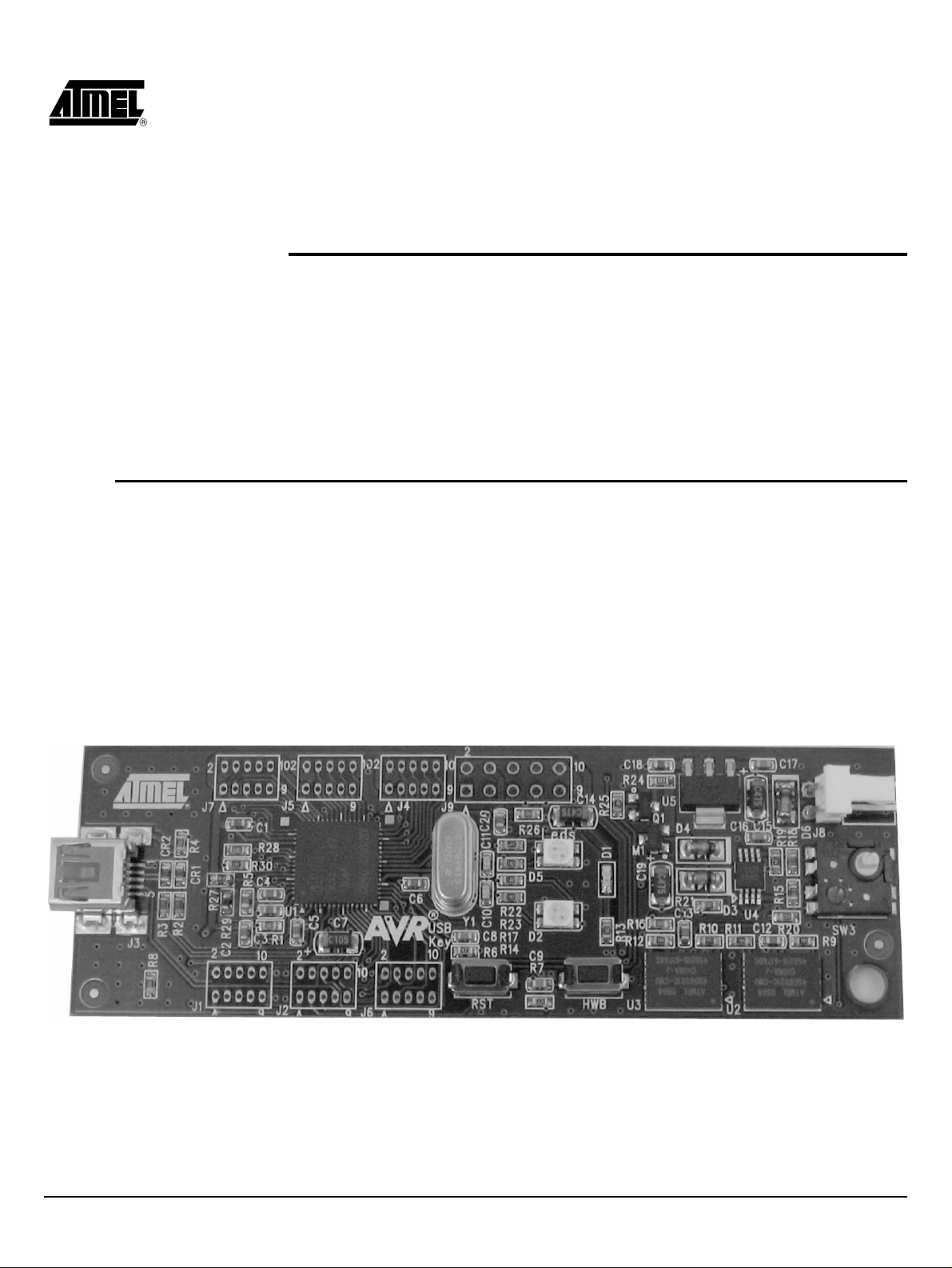
To increase its demonstrative capabilities, this stand alone board has numerous onboard resources: USB, joystick, data-flash and temperature sensor.
Figure 1-1 . AT90USBKey
AT90USBKey Hardware User Guide 1-3
7627A–AVR–04/06

Introduction
1.2 AT90USBKey Features
The AT90USBKey provides the following features:
AT90USB QFN64
AVR Studio® software interface
USB software interface for Device Firmware Upgrade (DFU bootloader)
Power supply flagged by “VCC-ON” LED:
JTAG interface (connector not mounted):
Serial interfaces:
On-board resources:
On-board RESET button
(1)
(2)
– regulated 3.3V
– from an external battery connector (for reduced host or OTG operation)
– from the USB interface (USB device bus powered application)
– for on-chip ISP
– for on-chip debugging using JTAG ICE
– 1 USB full/low speed device/host/OTG interface
– 4+1-ways joystick
– 2 Bi-Color LEDs
– temperature sensor
– serial dataflash memories
– all microcontroller I/O ports access on 2x8pin headers (not mounted)
On-board HWB button to force bootloader section execution at reset.
System clock:
– 8 MHz crystal
Notes: 1. The AVRUSBKey is supported by AVR Studio®, version 4.12 or higher. For up-to-
date information on this and other AVR tool products, please consult our web site.
The most recent version of AVR Studio®, AVR tools and this User Guide can be
found in the AVR section of the Atmel web site, http://www.atmel.com.
2. ATMEL Flip®, In System Programming Version 3 or Higher shall be used for Device
Firmware Upgrade. Please consult Atmel web site to retrieve the latex version of Flip
and the DFU bootloader Hex file if needed.
1-4 AT90USBKey Hardware User Guide
7627A–AVR–04/06
2.1 Overview
Section 2
Using the AT90USBKey
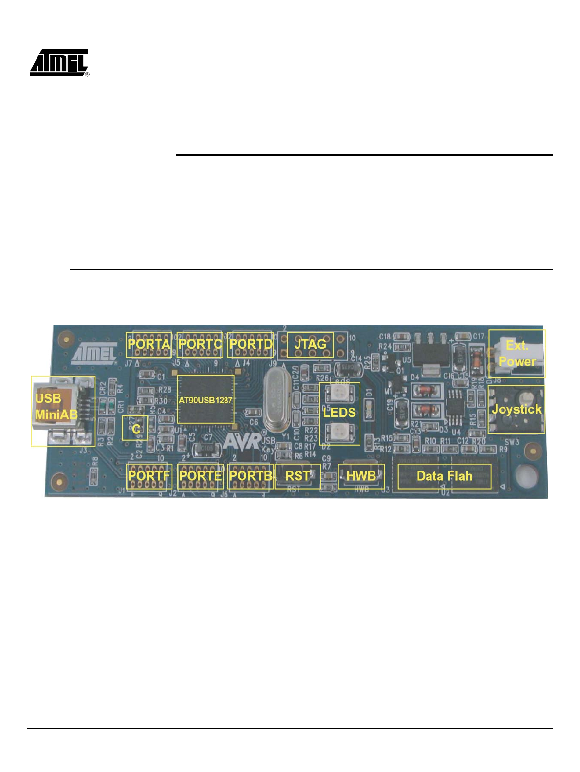
This chapter describes the AVRUSBKey and all its resources.
Figure 2-1 . AT90USBKey Overvi ew
AT90USBKey Hardware User Guide 2-5
7627A–AVR–04/06

Using the AT90USBKey
2.2 Power Supply
2.2.1 Power Supply Sources
USB powered When used as a US B devic e bus powered application, the AVRUSBKey can be direct ly
Battery powered The ex ternal battery connector should be used when the AT90USBKey is used as a
The on-board power supply circuitry allows two power supply configurations:
from USB connector
from battery connector
powered via the USB VBUS power supply line.
USB host. This mode allows the AT90USBKey to provide a 5V power supply from its
VBUS pin.
– Need of a female battery clip
– Input supply from 8 up to 15V DC (min. 100mA)
Figure 2-2 . P ower supply schematic
J8
2
1
MTA
Ext power supply
VBUS
D3
LL4148
D4
LL4148
D6
LL4148
5V
U4
2
IN
7
SHDN
3
GND
LP3982
U3out=1.25*(1+(R15+R18)/R19)
-
C16
4.7uF
220nF
C17
OUT
OUT
FAULT
CC
SET
VBAT
1
4
8
6
5
33nF
C15
1
2
U5
IN
GND
LM340
OUT
100k 1%
R19
124k 1%
3
100nF
C18
VCC3
VCC3
R15
R18100k 1%
2-6 AT90USBKey Hardware User Guide
7627A–AVR–04/06

2.2.2 VBUS Generator
Using the AT90USBKey
When using the AT90USB microcontroller in USB host mode, the AT90USBKey should
provide a 5V power supply over the VBUS pin of its USB mini AB connector.
A couple of transistors allows the UVCON pin of the AT90USB to control the VBUS
generation (See Figure 2-3). In this mode the AT90USBKey is powered by external
battery power supply source.
Figure 2-3 . VBUS generator schematic
FDV304P/FAI
UVCON
5V
R24
M1
10k
R25
Q1
BC847B
100k
-
C19
4.7uF
VBUS
2.2.3 “POWER-ON“ LED
The POWER-ON LED (“D1”) is always lit when power is applied to AVRUSBKey
regardless of the power supply source.
AT90USBKey Hardware User Guide 2-7
7627A–AVR–04/06

Using the AT90USBKey
2.3 Reset
Although the AT90USB has its on-chip RESET circuitry (c.f. AT90USB Datasheet,
section “System Control and Reset), the AVRUSBKey provides to the AT90USB a
RESET signal witch can come from two different sources:
Figure 2-4 . Reset Impleme n tatio n
VCC
2.3.1 Power-on RESET
2.3.2 RESET Push Button
2.3.3 Main Clock XTAL
R6
47k
RST
C8
220nF
RESET
The on-board RC network acts as power-on RESET.
By pressing the RESET push button on the AVRUSBKey, a warm RESET of the
AT90USB is performed.
To use the USB i nterface of the AT90USB, the clock s ource s hou ld a lways be a crystal
or external clock oscilla tor (the internal 8MHz RC oscilla tor can not be used to operate
with the USB interface). Only the following crystal frequency allows proper USB
operations: 2MHz, 4MHz, 6MHz, 8MH z, 1 2 MHz, 1 6 MHz. The AT90USBKey come s w ith
a default 8MHz crysta l os c illator.
2-8 AT90USBKey Hardware User Guide
7627A–AVR–04/06

2.4 On-board Resources
2.4.1 USB
The AVRUSBKey is supplied with a standard USB mini A -B receptacle. The mini AB
receptacle allows to connect both a mini A plug or a mini B plug connectors.
Figure 2-5 . USB mini A-B Receptacle
J3
1-V_BUS
5-GND
USB_MiniAB
2-D-
3-D+
4-ID
SHIELDSHIELDSHIELDSHIELD
VBUS
CR1
VBUS
CR2
R2 22
R3 22
C7
1uF
R4 0
Using the AT90USBKey
DD+
GND
UCAP
VBUS
GND
VBUS
UID
2.4.2 Joystick
When connecte d to a mini B plug, the AT90USB operates as an “US B device” (the ID
pin of the plug is unconnected) and when conne cted to a mini A plug, t he AT90USB
operates as a “USB host” (the ID pin of the A plug is tied to ground).
The 4+1 ways joystick offers an easy user interface implementation for a USB
application (it can emulate mouse movements, keyboard inputs ...).
Pushing the push-button causes the corresponding signal to be pulled low, while
releasing (not pressed) causes an H.Z state on the signal. The user must enable
internal pull-ups on the microcontroller input pins, removing the need for an external
pull-up resistors on the push-button.
Figure 2-6 . J oystick Schematic
PB[7..0]
PB[7..0]
SW3
SW3
SW3
1
1
1
2
2
2
TPA511G
TPA511G
TPA511G
Com1
Com1
Com1
Com2
Com2
Com2
Select
Select
Select
Left
Left
Left
Up
Up
Up
Right
Right
Right
Down
Down
Down
PB5
PB5
PB5
5
5
5
PB6
PB6
PB6
7
7
7
PB7
PB7
PB7
3
3
3
PE4
PE4
PE4
6
6
6
PE5
PE5
PE5
4
4
4
PB[7..0]
PE[7..0]
PE[7..0]
PE[7..0]
AT90USBKey Hardware User Guide 2-9
7627A–AVR–04/06

Using the AT90USBKey
2.4.3 LEDs
The AT90USBKey includes 2 bi-color LEDs (green/red) implemented on one line. They
are connected to the high nibble of “Port D” of AT90USB (PORTD[4..7]).
To light on a LED, the corresponding port pin must drive a high level. To light off a LED,
the corresponding port pin must drive a low level.
Figure 2-7 . LEDs Implementation schematic
LEDs
D2
D5
Table 2-1 . Leds references
LED Reference AT90USB Connection Color
D2 PORTD.4 Red
D5 PORTD.6 Green
In-line Grouped LED s
R141k
R171k
R221k
R231k
PORTD.5 Green
PORTD.7 Red
PD4
PD5
PD6
PD7
PD[7..0]
2.4.4 Temperature Sensor
The temperature sensor uses a thermistor (R29), or temperature-sensitive resistor. This
thermistor have a negat ive t emperatu re c oefficient (NTC ), mea ning the resistance goes
up as temperature goes down. Of all passive temperature measurement sensors,
thermistors have the highest sensitivity (resistance cha nge per degree of temperat ure
change). Thermistors do not have a linear temperature/resistance curve.
The voltage over the NTC can be found using the A/D converter (connected to channel
0). See the AT90USB Datasheet for how to use the ADC. The therm istor value (R
T) is
calculate with the following expression:
R
RHV
T
Where: RT = Thermistor value (Ω) at T temperature (°Kelvin)
⋅()VCC V
ADC0
H = Second resistor of the bridge -100 KΩ ±10% at 25°C
R
ADC0 = Volt age value on ADC-0 input (V)
V
VCC = Board power supply
2-10 AT90USBKey Hardware User Guide
7627A–AVR–04/06
–
()⁄=
ADC0

Using the AT90USBKey
The NTC thermistor used in AT90USBKey has a resistance of 100 KΩ ±5% at 25°C (T0)
and a beta-value of 4250 ±3%. By the use of the following equation, the temperature (T)
can be calculated:
T
Where: RT = Thermistor value (Ω) at T temperature (°Kelvin)
R
T
⎛⎞
ln
⎝⎠
-------
R
------+
T
0
β
0
β
-------------------------------=
ß = 4250 ±3%
0 = 100 KΩ ±5% at 25°C
R
0 = 298 °K (273 °K + 25 °K)
T
The following cross table also can be used. It is based on the above equation.
Table 2-2 . Thermistor Values versus Temperature
Temp.
(°C)
RT
(KΩ)
Temp.
(°C)
T
R
(KΩ)
Temp.
(°C)
T
R
(KΩ)
Temp.
(°C)
(KΩ)
-20 1263,757 10 212,958 40 50,486 70 15,396
-19 1182,881 11 201,989 41 48,350 71 14,851
-18 1107,756 12 191,657 42 46,316 72 14,329
-17 1037,934 13 181,920 43 44,380 73 13,828
-16 973,006 14 172,740 44 42,537 74 13,347
-15 912,596 15 164,083 45 40,781 75 12,885
-14 856,361 16 155,914 46 39,107 76 12,442
-13 803,984 17 148,205 47 37,513 77 12,017
-12 755,175 18 140,926 48 35,992 78 11,608
-11 709,669 19 134,051 49 34,542 79 11,215
-10 667,221 20 127,555 50 33,159 80 10,838
-9 627,604 21 121,414 51 31,840 81 10,476
-8 590,613 22 115,608 52 30,580 82 10,128
-7 556,056 23 110,116 53 29,378 83 9,793
-6 523,757 24 104,919 54 28,229 84 9,471
-5 493,555 25 100,000 55 27,133 85 9,161
T
R
-4 465,300 26 95,342 56 26,085 86 8,863
-3 438,854 27 90,930 57 25,084 87 8,576
-2 414,089 28 86,750 58 24,126 88 8,300
-1 390,890 29 82,787 59 23,211 89 8,035
0 369,145 30 79,030 60 22,336 90 7,779
1 348,757 31 75,466 61 21,498 91 7,533
2 329,630 32 72,085 62 20,697 92 7,296
3 311,680 33 68,876 63 19,930 93 7,067
4 294,826 34 65,830 64 19,196 94 6,847
AT90USBKey Hardware User Guide 2-11
7627A–AVR–04/06

Using the AT90USBKey
2.4.5 Data Flash memory
Temp.
(°C)
R
T
(KΩ)
Temp.
(°C)
T
R
(KΩ)
Temp.
(°C)
T
R
(KΩ)
Temp.
(°C)
T
R
(KΩ)
5 278,995 35 62,937 65 18,493 95 6,635
6 264,119 36 60,188 66 17,820 96 6,430
7 250,134 37 57,576 67 17,174 97 6,233
8 236,981 38 55,093 68 16,556 98 6,043
9 224,606 39 52,732 69 15,964 99 5,860
Figure 2-8 . Thermistor Schematic
PF[7..0]
VCC
PF0
R27
100k
R29
For mass-stora g e cla ss dem onstration purp o se , th e AT90 USBKe y p r o vides two on-chip
serial Flash memories (AT45DB642D) connected to the AT90 USB Serial Port Interface
(SPI).
PB[7..0]
VCC3
PE0
PB1
PB2
PB3
RESET
R9
100k
The data-flash chip select signals are connected to PortE bit 0 and bit 1 of the AT90USB
(See Figure 2-9).
Figure 2-9 . On-board data flash schematic
VCC3
R10
U2
1
SI
2
SCK
3
RESET
4
CS
AT45DB642D C ASON 8
SO
GND
VCC
WP
VCC3
8
7
6
5
R11
100k
PE1
PB1
PB2
PB3
RESET
100k
U3
1
SI
2
SCK
3
RESET
4
CS
AT45DB642D C ASON 8
SO
GND
VCC
WP
VCC3
8
7
6
5
R12
100k
2-12 AT90USBKey Hardware User Guide
7627A–AVR–04/06

2.5 In-System Programming
2.5.1 Programming with USB bootloader: DFU (Devi ce Firmware Upgrade)
AT90USB part comes with a default factory pre-programmed USB bootloader located in
the on-chip boot section of the AT90USB. This is the easiest and fastest way to
reprogram the device directly over the USB interface. The “Flip” PC side application, is
available from the Atmel website, offers a flexible an user friendly interface to reprogram
the application over the USB bus.
The HWB pin of the AT90USB allows to force the bootloader section execution after
reset. (Refer to AT90USB datasheet section “boot loa der support”). To force bootloader
execution, operate as follow:
Press both “RST” and “HWB” push buttons
First release the “RST” push button
Release the “HWB” push button
For more information about the USB bootloader and “Flip” application, please refer to
the “USB bootloader datasheet document” and “Flip’s user manual”.
Using the AT90USBKey
Note: The HWB pin is active only if the HWBE fuse is set (def ault factory conf iguration).
2.5.2 Programming with A VR JTAGI CEmKII
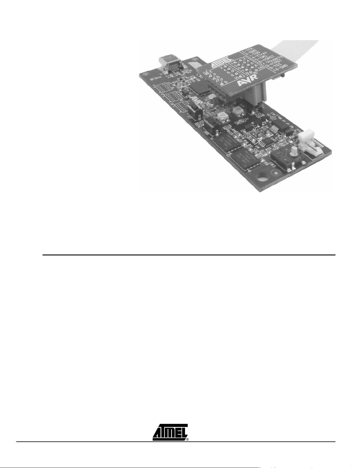
The AT90USB can be programmed using specific JTAG link. To use the AVR
JTAGICEmkII with an AT90USBKey an optional HE10 connector should be soldered to
J9 footprint. Then the JTAG probe c an be con nected t o the AT90USBKey as shown in
Figure 2-10.
Note: When the JTAGEN Fuse is unprogrammed, the four TAP pins are normal port pins, and
the TAP controller is in reset. When programmed, the input TAP signals are internally
pulled high and the JTAG is enabled for Boundary-scan and programming. The
AT90USB device is shipped with this fuse programmed.
AT90USBKey Hardware User Guide 2-13
7627A–AVR–04/06
Using the AT90USBKey
Figure 2-10 . Connecting AVR JTAG ICE to AVRUSBKey
The Flash, EEPROM and all Fuse and Lock Bit options ISP-programmable can be
programmed individually or with the sequential automatic programming option.
Note: See AVR Studio® on-line Help for informati on.
2.6 Debugging
2.6.1 Debugging with AVR JTAG ICE mkII
The AT90USBKey can be used for debugging with JTAG ICE MK II.
Connect the JTAG ICE mkII as shown in Figure 2-10, for debugging, please refer to
AVR Studio® Help information.
When using JTAG ICE MK II for debugging, and as AT90USB parts are factory
configured with the higher security level set, a chip erase operation will be performed on
the part before debugging. Thus the on-ch ip flash bootloader will be erased. It can be
restored after the debug session using the bootloader hex file available from ATM EL
website.
2-14 AT90USBKey Hardware User Guide
7627A–AVR–04/06

Troubleshooting Guide
Figure 3-1 . Troubleshooting Guide
Problem Reason Solution
The Green “VCC-ON”
LED is not on
No power supply
AVRUSBKey does not
work
Section 3
Verify the power supply source (check
battery char ge or USB connection).
The A T90USB cannot be
programmed
AVR Studi o does not
detect the AVR JTAG
ICE.
The A V R JTAG ICE
probe is not
connected
The memory lock bits
are programmed
The fuse bits are
wrongly programmed
Can not connect to
USB bootloader
Serial/USB cable is
not connected, or
power is off
PC COM port is in
use
Connect the JTAG ICE 10-PIN header to
the correct AVRUSBKey JTAG header
(page 13)
Erase the memory before programming
with JTAG ICE.
Check the fuse bits with JTAG ICE
Force bootloader execution with HWB
under reset.
USB bootloader erased after a JTAG
debugging session: reprogram the USB
bootloader with JTAG.
Connect seri al cable to RS232 (STK5 00 AVR ISP) and check power connect ions
Connect serial cable to USB (JATG ICE
MKII, AVR ISPmkIIl) and chec k power
connections
Disable other programs that are using
PC COM port.
Change PC COM port
AVR Studio does not
detect COM port.
AT90USBKey Hardware User Guide 3-15
Disable COM port auto-detect ion in AVR
St udio file menu. Force COM port to
correct COM port
7627A–AVR–04/06

Section 4
Technical Specifications
System Unit
– Physical Dimensions .....................................................L=90 x W=30 x H=8 mm
– Weight...........................................................................................................12 g
Operating Conditions
– Internal Voltage Supply .... ...........................................................................3.3V
– External Voltage Supply .........................................................................8V -15V
Connections
– USB Connector......................................................................Mini AB receptacle
– USB Communications .......................................................Full speed/low speed
– JTAG Connector....................................................Footprint for HE10 connector
– All ports connectors.............................................................J1, J2, J4, J5, J6, J7
– Battery connector....................................................................... MTA right angle
AT90USBKey Hardware User Guide 4-16
7627A–AVR–04/06

Section 5
Technical Support
For Technical support, please contact avr@atmel.com. When requesting technical
support, please include the following information:
Which target AVR device is used (complete part number)
Target vo ltage and speed
Clock source and fuse setting of the AVR
Programming method (ISP, JTAG or spec ific Boot-Loader)
Hardware revisions of the AVR tools, found on the PCB
Version number of AVR Studio. This can be found in the AVR Studio help menu.
PC operating system and version/build
PC processor type and speed
A detailed description of the problem
AT90USBKey Hardware User Guide 5-17
7627A–AVR–04/06

Section 6
Complete Schematics
On the next pages, the following documents of AT90USBKey are shown:
Complete schematics,
Bill of materials .
AT90USBKey Hardware User Guide 6-18
7627A–AVR–04/06

Figure 6-1 . Schematics, 1 of 2
Complete Schematics
Title
VCC
1
1
3
2
4
2
1
1
3
2
4
2
1.0.0
<Doc>
CPU
A4
Size Docum ent N um ber Rev
(not mounted)
1.27 mm D ual
H1.27-10
(not mounted)
1.27 mm D ual
H1.27-10
of
12Monday, J anuary 09, 2006
Date: Sheet
PE2
C9
220nF
C0603
PD[7..0]
C1
100nF
C0603
VCC
DECOUPLING CAPACITORS
CLOSED TO THE DEVI C E
MCU Pin52
C6
100nF
C0603
VCC
DECOUPLING CAPACITORS
CLOSED TO THE DEVI C E
MCU Pin21
C5
100nF
C0603
VCC
DECOUPLING CAPACITORS
CLOSED TO THE DEVI C E
MCU Pin3
VCC
PD7
PD5
PD3
PD1
3
5
7
9
5
7
9
6
8
10
J4
4
6
8
10
PD0
PD2
PD4
PD6
1
1
3
2
4
2
PC[7..0]
PC1
9
(not mounted)
1.27 mm D ual
H1.27-10
J5
10
PC0
R7
47k
VCC
PC7
PC5
PC3
(not mounted)
1
3
5
7
1
3
5
7
R0603
9
2
4
6
8
10
1.27 mm D ual
H1.27-10
2
4
6
8
PC2
PC4
PC6
C0603
R6
C8
47k
220nF
RESET
R0603
RESET
HWB
HWB
DTSM-3
Bootloader Activation
DTSM-3
A90USB Key
VCC
PE[7..0]
VCC
C0603
GND
PA3
PA4
PA5
PA6
PA7
PE2
PC7
PC6
PC5
PC4
PC3
PC2
PC1
42
43
48
PE2
PA744PA645PA546PA447PA3
PA2
49
PA2
PA1
PA0
PF7
PF6
PF5
PF4
PF3
PF2
PF1
PF0
AVCC
PA1
50
PA0
51
VCC
52
GND
53
PF7
54
PF6
55
PF5
56
PF4
57
PF3
58
PF2
59
PF1
60
PF0
61
AREF
62
GND
63
64
GND
AVCC
PE72UVcc3D-4D+5UGND6UCAP7VBUS8PE39PB010PB111PB212PB313PB414PB515PB6
PE6
AT90USB128U1QFN64
QFN64
1
PE6PE6
UVCON PE7
D-
UVCC
PB0
PB1
PB2
PB3
VBUS
D+
UID PE3
UCAP
PE7
PE5
PE3
PE1
1
3
5
7
9
1
3
5
7
9
2
4
6
8
10
J2
10
PE0
1.27 mm D ual
2
4
6
8
PE2
PE4
PE6
PF[7..0]
VCC
PF7
PF5
PF3
PF1
1
3
5
7
9
1
3
5
7
9
2
4
6
8
10
J1
10
PF0
1.27 mm D ual
2
4
6
8
PF2
PF4
PF6
PA[7..0]
(not mounted)
H1.27-10
PA[7..0]PA[7..0]PA[7..0]
PA[7..0]PA[7..0]PA[7..0]
VCC
(not mounted)
AGND
AREF
H1.27-10
C4
100nF
AREF
PF[7..0]
GND
VCC
UVCON
R2 22
R0603
C3
100nF
C0603
R1 0
VCC AVCC
C2
100nF
C0603
Ferrite & c apac it ors
closed t o t he MCU
VBUS
<ASSEMBLY>J3
D+ D- R ESI STORS
Closed t o t he MCU
VBUS
1-V_BUS
R0603
VBUS
UCAP
C7
1uF
C3216-A
R0603
R3 22
CR2
UGND UGNDUGNDUGNDUGND
2-D-
3-D+
5-GND
CR1
4-ID
SHIELDSHIELDSHIELDSHIELD
USB_MiniABF
MINI_USBC
PC0
PE1
34
PC035PC136PC237PC338PC439PC540PC641PC7
PB4
PB5
PGB0010603 R0603
PGB0010603 R0603
PE0
16
PB6
PC[7..0]
PC[7..0]
PD[7..0]
PE033PE1
PD7
PD6
PD5
PD4
PD3
PD2
PD1
PD0
XTAL1
XTAL2
GND
VCC
RESET
PE5
PE4
PB7
PD[7..0]
32
PD7
31
PD6
30
PD5
29
PD4
28
PD3
27
PD2
26
PD1
25
PD0
24
XTAL1
23
XTAL2
22
21
20
19
18
17
PE5
PE4
RESET
VCC
PB7
PB[7..0]PB[7..0]
UGND
R0603
R4 0
UCAP C apac it or
PB[7..0]
PE[7..0]
Closed t o t he MCU
R0603
R5 0
UGND
AGND
RST
RST
Reset Circuit
PA[7..0]
VCC
PA7
PA5
PA3
XTAL1
XTAL2
C11
15pF
C0603
8MHz
49US
Y1 8MHz CRY STAL
C10
15pF
C0603
PA1
3
5
7
9
5
7
9
6
8
10
J7
4
6
8
10
PA0
PA2
PA4
PA6
PB[7..0]
VCC
PB7
PB5
PB3
PB1
3
5
7
9
5
7
9
6
8
10
J6
4
6
8
10
PB0
PB2
PB4
PB6
R0603
R8 0
RESISTORS
CLOSED TO THE DEVI C E
AT90USBKey Hardware User Guide 6-19
7627A–AVR–04/06

Complete Schematics
Figure 6-2 . Schematics, 2 of 2
VCC3
UCAP
VCC
4
7
R15
8
OUT
SHDN
R16
100k 1%
6
5
CC
FAULT
3
LL4148
SET
VCC
R20
0
D4
R18100k 1%
C15
33nF
LP3982
LL4148
R21
0
0
5V
R19
124k 1%
U3out=1.25*(1+(R15+R18)/R19)
VCC3
D1
TOPLED LP M676
POWER LED(RED)
VCC
VCC
DECOUPLING CAPACITOR
CLOSE TO THE DEVIC E
C13
VCC3
C14
100nF
4.7uF
R13
1k
When mounting R21:
R20 not mounted
U4 not mounted
Allows to generate 3.3V
from U1 internal regulator
CAUTION: R21 default not mounted !!!
-
U4
D3
1
OUT
IN2GND
5V
VBUS
VCC3
U3
R12
100k
6
8
7
SO
GND
SI1SCK2RESET3CS
5
WP
VCC
AT45DB642D CASON 8
4
VBUS
FDV304P/FAI
M1
!!! R21 not mounted
R24
10k
C18
100nF
3
OUT
U5
IN1GND
LM340
2
VBAT
C17
220nF
C16
-
D6
LL4148
4.7uF
C19
4.7uF
-
of
22Saturday , F ebruary 18, 2006
Q1
BC847B
R25
100k
UVCON
VBUS generator f or OTG/HOST mode
1F <Cap Vbus < 6F OTG Specif ic at ion
VBAT
R28
VBat Mon.
220k
PF3
PF0
R27
VCC
Temp Sensor
100k
A90USB Key
<Doc> 1.0.0
Power & Interf ac es
A4
Title
Size D oc um ent N um ber Rev
Date: Sheet
R30
100k
R29
NCP18WF104J03RB
R10
VCC3
DECOUPLING CAPACITOR
CLOSE TO THE DEVIC E
C12
100nF
VCC3
Data Flash
PB[7..0]
VCC3
R9
100k
100k
VCC3
PE0
PE1
U2
PB1
PB1
PB3
PB2
R11
100k
6
7
8
SO
GND
SI1SCK2RESET3CS
PB3
PB2
RESET
5
VCC
4
RESET
WP
1
2
J8
PD[7..0]
PD4
AT45DB642D CASON 8
PD5
R141k
R171k
In-line Grouped LEDs
D2
PD7
PD6
R221k
R231k
D5
LEDs
MTA
PB[7..0]
PB5
5
SW3
Ext power supply
PB6
PE4
PB7
6
7
3
Up
Left
Select
Joystick Interface
Right
PE5
4
Down
PE[7..0]
Com11Com2
2
PF[7..0]
JTAG Interface
DECOUPLING CAPACITOR
R26
VCC
TPA511G
C20
100nF
VCC
RESET
8
4
6
2
CLOSE TO THE CONN EC TOR
J9
0
PF[7..0]
10
n.c.
VCC
GND
GND
RESET
CON 2x5
2.54 mm JTAG CON
TDI
9
PF7
CON 2x5
(not mounted)
TCK
TDO
TMS
VCC
1
3
5
7
PF4PF4
PF6
PF5PF5
6-20 AT90USBKey Hardware User Guide
7627A–AVR–04/06

Table 6-1 . Bill of material
Complete Schematics
Item Q.ty Reference Part
1 2 CR1,CR2 ESD protection (PGB0010603)
2 10 C1,C2,C3,C4,C5,C6,C12,
C13, C 18, C20
3 1 C7 1uF 10Vmin ±10% EIA/IECQ 3216
4 3 C8,C9, C17 220nF 50V-10% Cera m i c C ASE 0603
5 2 C10, C11 15pF 50V-5% Ceramic CASE 0603
6 3 C14, C16, C19 4.7uF 10Vmin ±10% EIA/IECQ 3216
7 1 C15 33nF 50V-5% Ceramic CASE 0603
8 2 D2,D5 LED BI-COLOUR/ LSGT670 I=10 mA_ PLCC-4
9 1 D1 TOPLED / LP M 6 76 - K2M 1 I=10 mA_ PLCC-2
10 2 D3,D4 DII LL4148-7 i=200mA max LL-34
11 1 J3 USB mini AB receptacle Surface mount
12 0 J9 CO N 2x 5 ( 2.5 4m m )
13 0 J1,J2,J4,J5 ,J6,J7 1.27 mm Dual header
14 1 J8 Connector MTA 2 cts right ang le
15 1 M1 FDV304P/FAI SOT23
16 1 Q1 BC847B IC peak=200mA SOT23
17 2 R2,R3 22 1/16W-5% SMD CASE 0603
18 1 R5 68k 1/16W-5% SMD CASE 0603
19 2 R6,R7 47k 1/ 1 6W-5% SMD CASE 0603
20 7 R1,R4,R5,R8,R16,R20, R26 0 CASE 0603
21 0 R21 0 (Not Mounted) CASE 0603
22 1 R28 220k 1/16W-5% SMD CASE 0603
23 7 R9,R10,R11,R12,R25,R27,R30100k 1/16W-5% SMD CASE 0603
100nF 50V-10% Ceramic CASE 0603
Tech.
Characteristics
(Not Mounted)
(Not Mounted)
Package
24 5 R13,R14,R17,R22,R23 1k 1/16W-5% SMD CASE 0603
25 2 R24 , R2 8 10k 1/16W-5% SMD CASE 0603
26 1 R29 NCP18WF104J03RB 100K - ß=4250 CASE 0603
27 2 R15,R18 100k 1% 1/16W-1% SMD CASE 0603
28 1 R19 120k 1% 1/16W-1% SMD CASE 0603
29 2 SW1,SW2 PUSH-BU TTON / DTSM31N 6x3.5mm - 1.6N See DS
30 1 SW3 TPA511G 4 ways joystic k + center CMS mount
31 1 U1 AT90USB1287 QFN64
32 2 U2,U3 AT45DB642D CASON8
33 1 U4 LP3982IMM-ADJ Vin Max 6V, 300mA MSOP8
34 1 U6 LM340MP5.0
35 1 Y1 8MHz CRYSTA L H=4mm HC49/4H
AT90USBKey Hardware User Guide 6-21
7627A–AVR–04/06

Atmel Corporation Atmel Operations
2325 Orchard Park way
San Jose, CA 95131, USA
Tel: 1(408) 4 41-0311
Fax: 1(408) 487-260 0
Regional Headquarters
Europe
Atmel Sa rl
Route des Ars enau x 41
Case Postale 8 0
CH-1705 Fri bourg
Switzerland
Tel: (41) 26-4 26-55 55
Fax: (41) 26 -426-550 0
Asia
Room 121 9
Chinachem Gold en Plaza
77 Mody Ro ad Tsims hatsu i
East Kowloon
Hong Kong
Tel: (852) 27 21-9778
Fax: (852) 2 722-136 9
Japan
9F, Tonetsu Sh inkaw a Bl dg.
1-24-8 Shi nkawa
Chuo-ku, Tok yo 10 4-0033
Japan
Tel: (81) 3-35 23-35 51
Fax: (81) 3-3 523-758 1
Memory
2325 Orch ard Parkw ay
San Jose, C A 95131 , USA
Tel: 1(408 ) 441-031 1
Fax: 1(408) 43 6-43 14
Microcontrollers
2325 Orch ard Parkw ay
San Jose, C A 95131 , USA
Tel: 1(408 ) 441-031 1
Fax: 1(408) 43 6-43 14
La Chantrer ie
BP 70602
44306 Na ntes Cede x 3, Fra nce
Tel: (33) 2-4 0-18 -18-18
Fax: (33) 2-40-18-19-60
ASIC/ASSP/Smart Cards
Zone In dustrielle
13106 Rousse t Ced ex, France
Tel: (33) 4-4 2-53 -60-00
Fax: (33) 4-42-53-60-01
1150 East C heyenn e Mtn. Blvd.
Colorado Sp rings, CO 8 0906, USA
Tel: 1(719 ) 576-330 0
Fax: 1(719) 54 0-17 59
Scottish Enterprise Technology Park
Maxwell Building
East Kilbrid e G7 5 0QR, S cotlan d
Tel: (44) 13 55-803- 000
Fax: (44) 1355 -242 -743
RF/Automotive
Theresienstrasse 2
Postfach 3535
74025 Heilbr onn, Ge rmany
Tel: (49) 71-31-67-0
Fax: (49) 71 -31-67- 2340
1150 East Ch eyenne M tn. B lvd.
Colorado Spr ings, CO 80 906, USA
Tel: 1(719) 57 6-3300
Fax: 1(719) 540-1759
Biometrics/Imaging/Hi-Rel MPU/
High Speed Converters/RF Datacom
Avenue de R ocheplei ne
BP 123
38521 Saint- Egreve Cedex, France
Tel: (33) 4-76-58-30-00
Fax: (33) 4-7 6-58-3 4-80
Literature Requests
www.atmel.com/literature
Disclaimer: The information in this document is provided in connection with Atmel products. No license, express or implied, by estoppel or otherwise,to anyintellectualproperty right is granted by this document or in connection with the sale of Atmel products. EXCEPT AS SET FORTH IN ATMEL’S TERMS AND CONDI-TIONS OF
SALE LOCATED ON ATMEL’S WEB SITE, ATMEL ASSUMES NO LIABILITY WHATSOEVER AND DISCLAIMS ANY EXPRESS, IMPLIED OR STATUTORYWARRANTY RELATING TO ITS PRODUCTS INCLUDING, BUT NOT LIMITED TO, THE IMPLIED WARRANTY OF MERCHANTABILITY, FITN ESS FOR A PARTICULARPURPOSE, OR NON-INFRINGEMENT. IN NO EVENT SHALL ATMEL BE LIABLE FOR ANY DIRECT, INDIRECT, CONSEQUENTIAL, PUNITIVE, SPECIAL
OR INCIDEN-TAL DAMAGES (INCLUDING, WITHOUT LIMITATION, DAMAGES FOR LOSS OF PROFITS, BUSINESS INTERRUPTION, OR LOSS OF INFORMATION) ARISING OUTOF THE USE OR INABILITY TO USE THIS DOCUMENT, EVEN IF ATMEL HAS BEEN ADVISED OF THE POSSIBILITY OF SUCH DAMAGES. Atmel makes nor epresentationsor warranties with respect to the accuracy or completeness of the contents of this docum ent and reserves the right to make
changes to specificationsand product descriptions at any time without notice. Atmel does not make any commitment to update the information contained herein.
Unless specifically provided otherwise, Atmel products are not suitable for, and shall not be used in, automotive applications. Atmel’s products are not intended,
authorized, or warranted for useas components in applications intended to support or sustainlife.
© Atmel Co rpora tion 20 06. All rights reserved. Atmel®, logo and combinations thereof, are registered trademarks, and Everywhere You Are
are th e trade ma r k s of A tm el C o rporatio n o r i ts s u bs idiarie s. O the r t er m s an d pr o du c t names m a y be tra de m ar k s of others.
Printed on recy cled paper.
7627A–AVR–04/06
/xM
®
 Loading...