

Datasheet AT90S8515-8JI, AT90S8515-8JC, AT90S8515-8AI, AT90S8515-4PI, AT90S8515-4PC Datasheet (ATMEL)
...
Features
•
AVR - High Performance and Low Power RISC Architecture
•
118 Powerful Instructions - Most Single Clock Cycle Execution
•
8K bytes of In-System Reprogrammable Flash
– SPI Serial Interface for Program Downloading
– Endurance: 1,000 Write/Eras e Cycles
•
512 bytes EEPROM
– Endurance: 100,000 Write/Erase Cycles
•
512 bytes Internal SRAM
•
32 x 8 General Purpose Working Registers
•
32 Programmable I/O Lines
•
Programmable Serial UART
•
SPI Serial Interface
•
VCC: 2.7 - 6.0V
•
Fully Static Operation
– 0 - 8 MHz 4.0 - 6.0V,
– 0 - 4 MHz 2.7 - 4.0V
•
Up to 8 MIPS Throughput at 8 MHz
•
One 8-Bit Timer/Counter with Separate Prescaler
•
One 16-Bit Timer/Counter with Separate Prescaler
and Compare and Capture Modes
•
Dual PWM
•
External and Internal Interrupt Sources
•
Programmable Watchdog Timer with On-Chip Oscillator
•
On-Chip Analog Comparator
•
Low Power Idle and Power Down Modes
•
Programming Lock for Software Security
8-Bit
Microcontroller
with 8K bytes
In-System
Programmable
Flash
AT90S8515
Description
The AT90S8 515 is a low-p ower CMOS 8-bit mic rocontroll er based on the AVR
enhanced RISC architecture . By exe cuting powe rful instruc tions in a single clock
cycle, the AT90S8515 achieves throughpu ts approaching 1 MIPS per MHz allowing
the system designer to optimize power consumption versus processing speed.
The AVR core combines a rich instr uction set with 32 gene ral purpose working registers. All the 32 registers are directly connected to the Arithmetic Logic Unit (ALU),
allowing two indep endent r egisters to be acce ssed in one singl e instr uction execute d
in one clock cycle. Th e resulting arc hitecture is mor e code efficie nt while achievin g
throughputs up to ten times faster than conventional CISC microcontrollers.
(continued)
Pin Configurations
Preliminary
®
Rev. 0841D–06/98
1
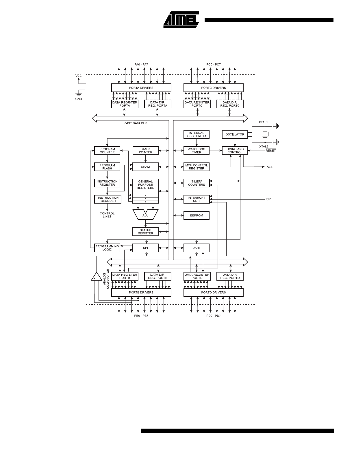
Block Diagram
Figure 1.
The AT90S8515 Block Diagram
The AT90S8515 provides the following features: 8K bytes
of In-System Programmable Flash, 512 bytes EEPROM,
512 bytes SRAM, 32 gen eral purpo se I/O li nes, 3 2 general
purpose working registers, flexible timer/counters with
compare modes, internal and external interrupts, a programmable serial UART, programmable Watchdog Timer
with internal oscillator, an SPI serial port and two software
selectable pow er saving modes. T he Idl e Mode sto ps the
CPU while allowing the SRAM, timer/counters, SPI port
and interrupt syste m to contin ue functioning . The power
down mode saves the register contents but freezes the
oscillator, disabling all other chip functions until the next
interrupt or hardware reset.
2
AT90S8515
The device is manufac tured using Atmel’ s high density
non-volatile memory technology. The on-chip in-system
programmable Flash allows the program memory to be
reprogrammed in-sys tem th ro ugh an S PI se rial i nterface or
by a conventional n onvolatile memo ry programmer. By
combining an enhanced RISC 8-bit CPU wit h In-System
Programmable Flash on a monolithic chip, the Atmel
AT90S8515 is a powerful microcontroller that provides a
highly flexible and co st effect ive solution to many em bedded control applications.
The AT90S8515 AVR is supported with a full s uite of program and system development tools including: C compilers, macro assemblers, program debugger/si mulators, incircuit emulators, and evaluati on kits.
AT90S8515
Pin Descriptions
V
CC
Supply voltage
GND
Ground
Port A (PA7..PA0)
Port A is an 8 -bit b idirec tional I/O port. Port p ins ca n provide internal pull-up resistors (selected for each bit). The
Port A output buffers can sink 20mA and can drive LED displays directly. When pins PA0 to PA7 are used as inputs
and are externally pull ed low, they will source c urrent if the
internal pull-up resistors are activated.
Port A serves as Multiplexed Address/Data input/output
when using external SRAM.
Port B (PB7..PB0)
Port B is an 8-bit bidirectional I/O pins with internal pull-up
resistors. The Port B output buffers can sink 20 mA. As
inputs, Port B pins t hat a re ex ter nally pu ll ed l ow wi ll sour c e
current if the pull-up resistors are activated.
Port B also serves the fu nction s of vario us speci al feat ures
of the AT90S8515 as listed on page 46.
Port C (PC7..PC0)
Port C is an 8-bit bidirectional I/O port with internal pull-up
resistors. The Port C output buffers can sink 20 mA. As
inputs, Port C pins that are exter nal ly pul led low wil l sour ce
current if the pull-up resistors are activated.
Port C als o s erv es as Addr es s ou tp ut when us ing ext ern al
SRAM.
Port D (PD7..PD0)
Port D is an 8-bit bidirectional I/O port with internal pull-up
resistors. The Port D output buffers can sink 20 mA. As
inputs, Port D pins that are exter nal ly pul led low wil l sour ce
current if the pull-up resistors are activated.
Port D also serves th e fu nc tion s of v ario us sp ec ial fea tur es
of the AT90S8515 as listed on page 52.
RESET
Reset input. A low on th is pi n for two machi ne cy cles wh ile
the oscillator is running resets the device.
XTAL1
Input to the inverting os cillator amplifi er and input to th e
internal clock operating circuit.
XTAL2
Output from the inverting oscillator amplifier
ICP
ICP is the input pin for the Time r/Counter1 Inpu t Capture
function.
OC1B
OC1B is the output pin for the Timer/Counter1 Output
CompareB function
ALE
ALE is the Address Latch Enable used when the Ex ternal
Memory is enabled. The ALE strob e is used to latch the
low-order address (8 bits) into an address latch during the
first access cy cle, and the A D0-7 pins a re used for data
during the second access cycle.
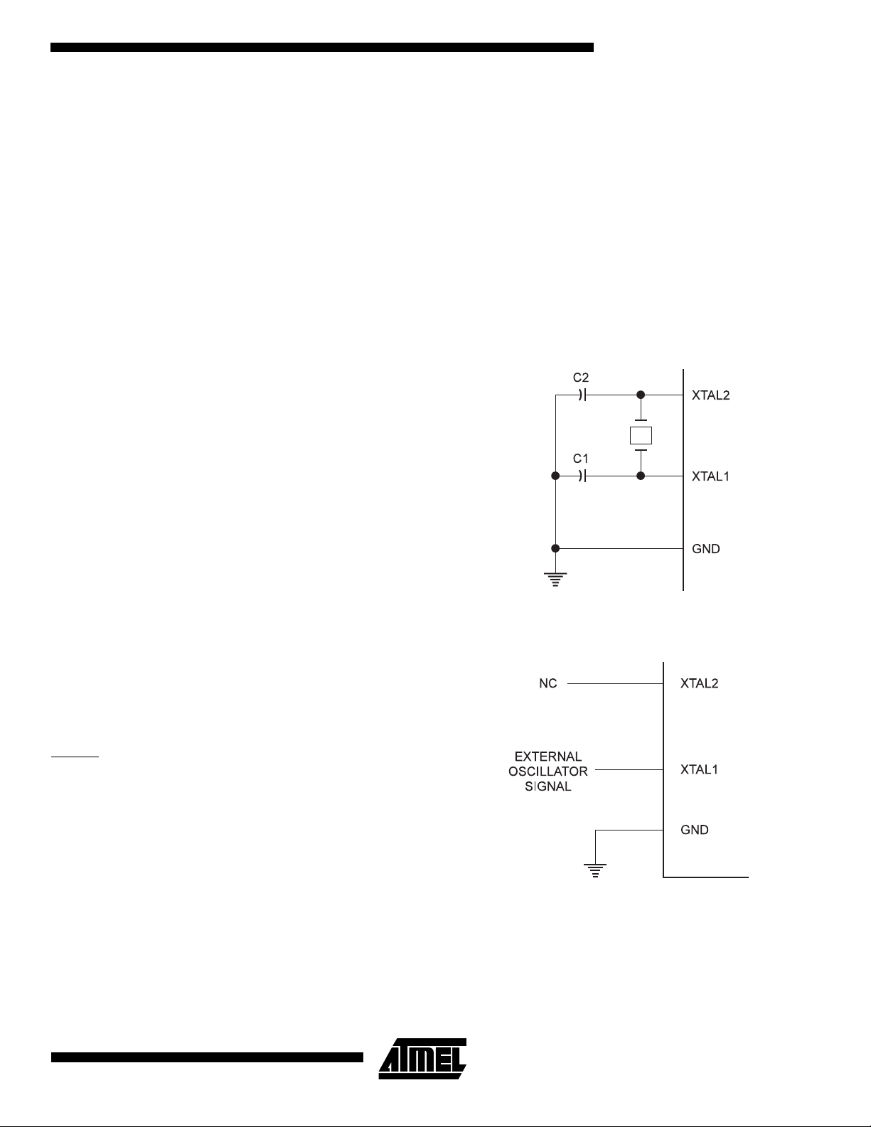
Crystal Oscillator
XTAL1 and XTAL2 are input and output, respectively, of an
inverting amplifier which can be configured for use as an
on-chip oscillator, as shown in Figure 2. Either a quartz
crystal or a ceramic resonator may be used. To drive the
device from an external clock source, XTAL2 should be left
unconnected while XTAL1 is driven as shown in Figure 3.
Figure 2.
Figure 3.
Oscillator Connec tio ns
External Clock Drive Configuration
3
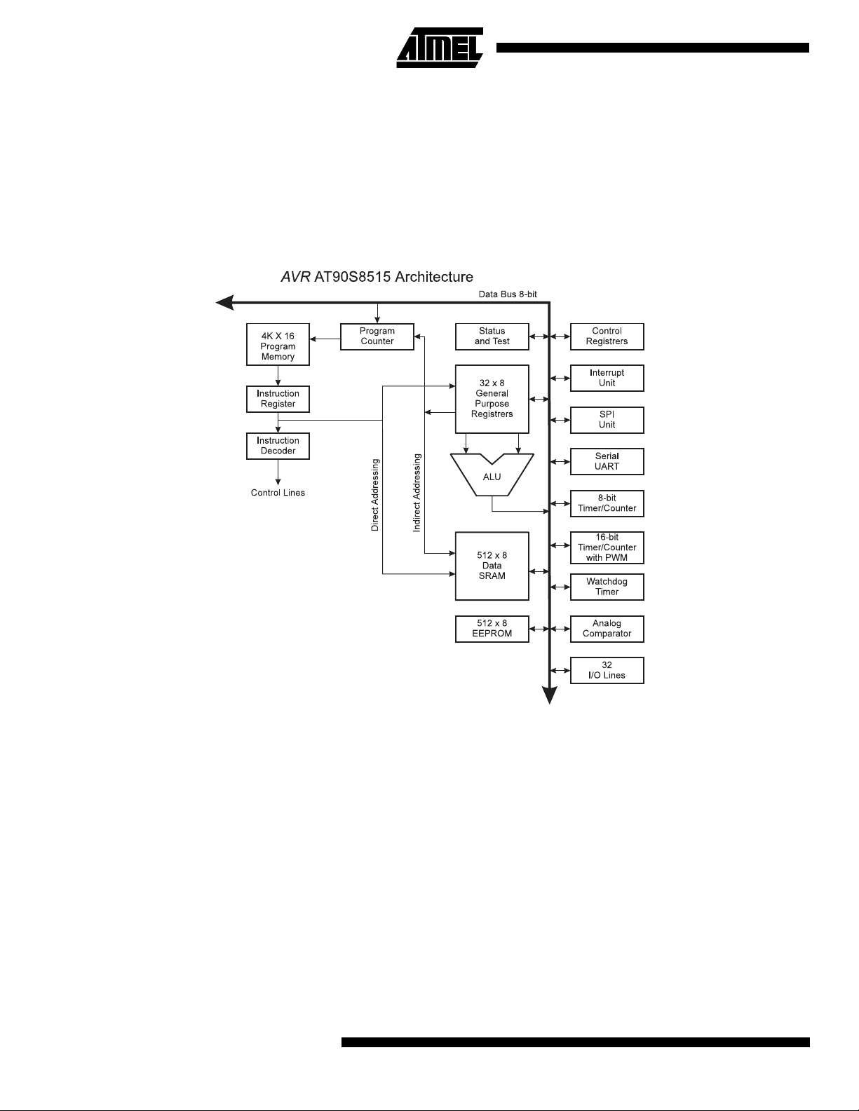
AT90S8515 Architectural Overview
The fast-access register file concept contains 32 x 8-bit
general purpose worki ng regi ster s with a sin gle cl ock c ycle
access time. This means that during one single clock cycle,
one ALU (Arithmetic Logic Unit) operation is executed. Two
operands are output from the register file, the operation is
executed, and the result is stored back in the register file in one clock cycle.
Six of the 32 registers can be used as three 16-bits indirect
address register pointers for Data Space addressing enabling efficient address calculati ons. One of the three
address pointers is also used as the address pointer for the
constant table look up function. These added function registers are the 16-bits X-register, Y-register and Z-register.
Figure 4.
The AT90S8515
AVR
Enhanced RISC Architecture
The ALU supports arithmetic and logic functions between
registers or be tween a const ant and a r egist er. Si ngle re gister operations are also executed in the ALU. Figure 4
shows the AT90S851 5 AVR Enhan ced RISC mi crocontro ller architecture .
In addition to the register operation, the conventional memory addressing mode s can be used on the re gister file as
well. This is e nabled by th e fact that t he register f ile is
assigned the 32 lowermost Data Space addresses ($00 $1F), allowing them to be accessed as though they were
ordinary memory locations.
The I/O memory space contains 64 addresses for CPU
peripheral functions as Control Registers, Timer/Counters,
A/D-converte rs, and ot her I/O fun ctions. T he I/O Mem ory
can be accessed dir ectly, or as the Da ta Space loca tions
following those of the register file, $20 - $5F.
4
AT90S8515
AVR
The
rate memories and buses fo r program and data. The pr ogram memory is executed with a two stage pipeline. While
one instruction is bein g executed, the next ins truction is
pre-fetched from the program memory. This co ncept
enables instructions to be executed in every clock cycle.
The program memory is in-system programmable Flash
memory.
With the relat ive jump an d call i nstructi ons, the w hole 4K
address space i s directl y access ed. Most AVR in struc tions
have a single 16-bit word format. Every program memory
address contains a 16- or 32-bit instruction.
During interrupts and su broutine calls, t he retur n addre ss
program counter (PC) is stor ed on the stack. The stack is
effectively allo cated i n the gene ral dat a SRAM, and cons equently the stack size is only limited by the total SRAM size
and the usage of the SR AM. All user progr ams must initial-
uses a Harvard architecture concept - with sepa-
AT90S8515
ize the SP in the reset routine (before subroutines or inter-
Figure 5.
Memory Maps
rupts are execute d). The 16-bit stack pointer SP is
read/write accessib le in the I/O spac e.
The 512 bytes data SRAM can be easily access ed through
the five different addressing modes supported in th e AVR
architecture.
The memory spaces in the AVR
architecture are all linear
and regular memory maps.
A flexible interrupt module has its control registers in the
I/O space with an additional global interrupt enable bit in
the status register. All the different interrupts have a separate interrupt vector in the interrupt vector table at the
beginning of the program memory. The different interrupts
have priority in accordance with their interrupt vector position. The lower the interrupt vector address the higher the
priority.
The General Purpose Register File
Figure 6 shows the structure of the 32 general purpose working registers in the CPU.
Figure 6.
AVR CPU General Purpose Working Registers
70Addr.
R0 $00
R1 $01
R2 $02
…
R13 $0D
General R14 $0E
Purpose R15 $0F
Working R16 $10
Registers R17 $11
…
R26 $1A X-register low byte
R27 $1B X-register high byte
R28 $1C Y-register low byte
R29 $1D Y-register high byte
R30 $1E Z-register low byte
R31 $1F Z-register high byte
All the register operating instructions in the i nstruction set
have direct and single cycle access to all registers. The
only exceptio n is the five consta nt arithmetic and logic
instructions SB CI, SUBI , CPI, ANDI and ORI between a
constant and a register and the LDI instruction for load
immediate constant data. These instructions apply to the
second half of the registers in the register file - R16..R31.
The general SBC, SUB, CP, AND and OR and all other
operations between two register s or on a s ingle regis ter
apply to the entire register file.
As shown in Figure 6, each register is also assigned a data
memory address, mapp ing them direc tly into the fi rst 32
locations of the user Data Space. Although not being physically implemented as SRAM locations, this memory organization provides great flexibility in access of the registers,
as the X,Y and Z registers ca n be set to index an y register
in the file.
5

The X-Register, Y-Register And Z-Register
The registers R26..R31 have some added functions to their
general purpose usa ge. Thes e re gister s a re ad dr es s poi nt-
ers for indirect addressing of the Data Space. The three
indirect address registers X, Y and Z are defined as:
Figure 7.
The X, Y and Z Registers
15 0
X - register 7 0 7 0
R27 ($1B) R26 ($1A)
15 0
Y - register 7 0 7 0
R29 ($1D) R28 ($1C)
15 0
Z - register 7 0 7 0
R31 ($1F) R30 ($1E)
In the different addressing modes these address registers
have functions as f ixed d ispl acement , a utoma tic in cre ment
and decrement (see the descriptions for the different
instructions).
The ALU - Arithmetic Logic Unit
The high-performance AVR ALU operates in direct connection with all the 32 general purpose working registers.
Within a single clo ck cy cle, AL U oper ations b etween regi sters in the register fil e are executed . The ALU operat ions
are divided into three main categories - arithmetic, logical
and bit-functions.
The In-System Programmable Flash Program
Memory
The AT90S8515 contain s 8K byt es on- chip In- System Programmable Flash memory for program storage. Since all
instructions are 16-or 32-bit words, the Flash is organized
as 4K x 16. The Flash memo ry has an endurance of at
least 1000 write/erase cyc les. The AT90S85 15 Program
Counter (PC) is 12 bits wide, thus addressing the 4096 program memory addresses.
See page 62 for a detailed description on Flash data downloading.
Constant tables mu st be alloc ated wit hin the ad dress 0-4K
(see the LPM - Load Program Memory instruction description).
See page 8 for the different program memory addressing
modes.
6
AT90S8515
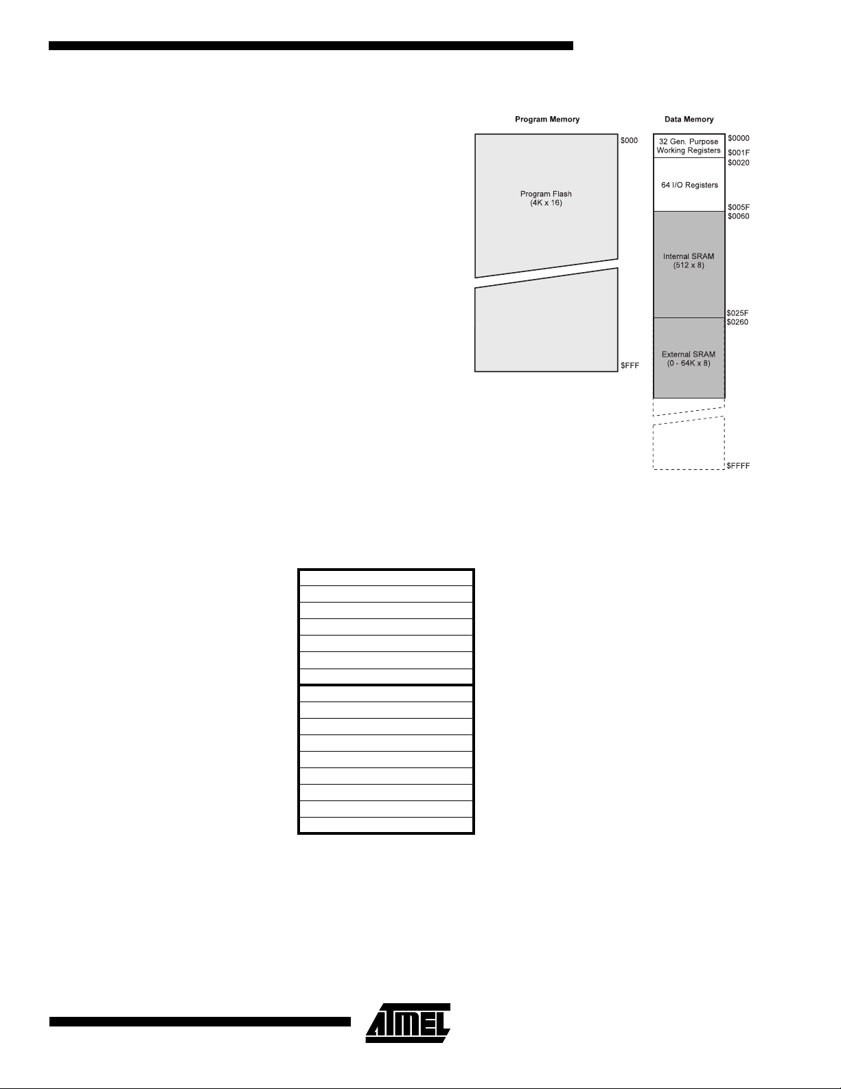
The SRAM Data Memory - Internal and External
The following figure shows how the A T90S8515 SRAM
Memory is organized:
AT90S8515
Figure 8.
SRAM Organization
Register File Data Address Space
R0 $0000
R1 $0001
R2 $0002
……
R29 $001D
R30 $001E
R31 $001F
I/O Registers
$00 $0020
$01 $0021
$02 $0022
……
$3D $005D
$3E $005E
$3F $005F
Internal SRAM
$0060
$0061
…
$025E
$025F
External SRAM
$0260
$0261
…
The lower 608 Data Memory locations address the Register file, the I/O Memory and the internal data SRAM. The
first 96 locations address the Register File + I/O Memo ry,
and the next 512 locations addres s the internal data
SRAM. An optiona l externa l data S RAM can be placed in
the same SRAM memory space. This SRAM will oc cupy
the location following the internal SRAM and up to as much
as 64K - 1, depending on SRAM size.
When the addresses accessing the data memory space
exceeds the internal data SRAM locations, the external
data SRAM is acc essed usi ng the sam e inst ructions as for
the internal data SRAM access. When the internal data
space is accessed, the read a nd write s trobe pins (RD and
) are inactive during the wh ole access c ycle. External
WR
SRAM operation is enabled by setting the SRE bit in the
MCUCR register. See page 21 for details.
$FFFE
$FFFF
Accessing external SRAM takes one additional clock cycle
per byte compared to access of the internal SRAM. This
means that the commands LD, ST, LDS, STS, PUSH and
POP take one additional clock cycle. If the stack is placed
in external SRAM, interrupts, subr outine calls and returns
take two clock cycles extra because the two-byte program
counter is pushed and popped. When external SRAM interface is used with wait state, two additional cloc k cycles is
used per byte. This has the follo wing effect: Data transfer
instructions take two extra clock cycles, whereas interrupt,
subroutine calls and returns will need four clock cycles
more than specified in the instruction set manual.
The five differen t address ing modes for the data mem ory
cover: Direct, Indirect with Displacement, Indirect, Indirect
with Pre-Decrement and Indirect with Post-Increment. In
the register file, registers R26 to R31 feature the indirect
addressing pointer registers.
7
The direct addressing reaches the entire data space.
The Indirect with Displacement mode features a 6 3
address locations reach from the base address given by
the Y or Z-r egister.
When using register indirect addressing modes with automatic pre-decr ement and post-in crement , the addr ess registers X, Y and Z are decremented and incremented.
The 32 general purpose working registers, 64 I/O registers,
the 512 bytes of i ntern al da ta SR AM, a nd the 64K bytes of
optional external da ta SRAM in the AT90S8515 are all
accessible through all these addressing modes.
See the next secti on for a det ailed desc ription of the differ ent addressing modes.
The Program and Data Addressing Modes
The AT90S8515
ports powerful and efficie nt addressing modes for access
to the program memory (Flash) and data memory (SRAM,
Register File and I/O Memory). This section describes the
different addressing modes supported by the
ture. In the figures, OP means the operation code part of
the instruction word. To simplify, not all figures show the
exact location of the addressing bits.
Register Direct, Single Register RD
AVR
Enhanced RISC microcontroller sup-
AVR
architec-
Operands are contained in register r (Rr) and d (Rd). T he
result is stored in register d (Rd).
I/O Direct
Figure 11.
Operand address is contained in 6 bits of the instruction
word. n is the destination or source register address.
Data Direct
Figure 12.
I/O Direct Addressing
Direct Data Addressing
Figure 9.
The operand is contained in register d (Rd).
Register Direct, Two Registers RD AND RR
Figure 10.
Direct Single Register Addressing
Direct Register Addressing, Two Registers
A 16-bit Da ta Ad dr ess is containe d in t h e 16 L SB s o f a t w o word instruction. Rd/Rr specify the destination or source
register.
Data Indirect With Displacement
Figure 13.
Data Indirect with Displacement
Operand address is the result of the Y or Z-register contents added to the address contained in 6 bits of the
instruction wo rd .
8
AT90S8515
AT90S8515
Data Indirect
Figure 14.
Operand address is t he contents of the X, Y or the Z-re gi ster.
Data Indirect With Pre-Decrement
Figure 15.
Data Indirect Addressing
Data Indirect Addressing With Pre-Decrement
Constant Addressing Using The LPM Instruction
Figure 17.
Constant byte address is specified by the Z-register contents. The 15 MSBs sel ec t wo rd ad dres s (0 - 4 K) an d L SB ,
select low byte i f clear ed (LSB = 0) or high b yte if set ( LSB
= 1).
Indirect Program Addressing, IJMP and ICALL
Figure 18.
Code Memory Constant Addressing
Indirect Program Memory Addressing
The X, Y or the Z-register is decremented before the operation. Operand address is the decremented contents of the
X, Y or the Z-register.
Data Indirect With Post-Increment
Figure 16.
The X, Y or the Z- register is incr emented af ter the oper ation. Operand address is the content of the X, Y or the Zregister prior to incrementing.
Data Indirect Addressing With Post-Increment
Program execution continues at address contained by the
Z-register (i.e. the PC is loaded with the contents of the Zregister).
Relative Program Addressing, RJMP and RCALL
Figure 19.
Program execution continues at add ress PC + k + 1. The
relative address k is -2048 to 2047.
Relative Program Memory Addressing
9
The EEPROM Data Memory
The AT90S8515 contains 512 bytes of data EE PROM
memory. It is organized as a separate data space, in which
single bytes can be read and written. The EEPROM has an
endurance of at least 100,000 write/erase cycles. The
access between the EEPROM and the CPU is described
on page 32 sp ecifyi ng the EEPRO M address r egisters, the
EEPROM data register, and the EEPROM control register.
For the SPI data downloading, see page 62 for a detailed
description.
Memory Access Times and Instruction
Execution Timing
This section describes the general access timing concepts
for instruction execution and internal memory access.
AVR
The
generated from th e external clock cryst al for the chip. No
internal clock division is used.
Figure 20 shows the parallel instr uction fetches and
instruction executions enabled by the Harvard architecture
and the fast-access register file concept. This is the basic
pipelining concep t to ob tai n up to 1 MIP S per MHz with the
corresponding unique results for functions per cost, functions per clocks, and functions per power-unit.
CPU is driven by the System Clock Ø, directly
Figure 20.
The Parallel Instruction Fetches and Instruction Executions
T1 T2 T3 T4
System Clock Ø
1st Instruction Fetch
1st Instruction Execute
2nd Instruction Fetch
2nd Instruction Execute
3rd Instruction Fetch
3rd Instruction Execute
4th Instruction Fetch
Figure 21 shows the in ter nal ti min g c oncept for the register
file. In a single clock cycle an ALU operation using two reg-
Figure 21.
Single Cycle ALU Operation
T1 T2 T3 T4
System Clock Ø
Total Execution Time
Register Operands Fetch
ALU Operation Execute
ister operands is executed, and the r esult is stored bac k to
the destination register.
Result Write Back
The internal data SRAM access is performed in two System Clock cycles as described in Figure 22.
10
AT90S8515
AT90S8515
Figure 22.
On-Chip Data SRAM Access Cycles
T1 T2 T3 T4
System Clock Ø
Address
Prev. Address
Address
Data
WR
Data
RD
The external data SRAM access is performed in two System Clock cycles as described in Figure 22.
Figure 23.
External Data SRAM Memory Cycles without Wait State
T1 T2 T3
System Clock Ø
ALE
Address [15..8]
Prev. Address
Address
Read Write
Data / Address [7..0]
Prev. Address
Address
Data
Address
WriteRead
WR
Data / Address [7..0]
Prev. Address
Address
Data
Address
RD
The external data SRAM memory access cycle with the Wait State bit enabled (Wait State active) is shown in Figure 24.
Figure 24.
External Data SRAM Memory Cycles with Wait State
T1 T2 T3 T4
System Clock Ø
ALE
WR
RD
Prev. Address
Prev. Address
Prev. Address
Address
Address
Address [15..8]
Data / Address [7..0]
Data / Address [7..0]
Address
Data
Data
Addr.
WriteRead
Addr.
11

I/O Memory
The I/O space definition of the AT90S8515 is shown in the following table:
Table 1.
AT90S8515 I/O Space
Address Hex Name Function
$3F ($5F) SREG Status Register
$3E ($5E) SPH Stack Pointer High
$3D ($5D) SPL Stack Pointer Low
$3B ($5B) GIMSK General Interrupt Mask register
$3A ($5A) GIFR General Interrupt Flag Register
$39 ($59) TIMSK Timer/Counter Interrupt Mask register
$38 ($58) TIFR Timer/Counter Interrupt Flag register
$35 ($55) MCUCR MCU general Control Register
$33 ($53) TCCR0 Timer/Counter0 Control Register
$32 ($52) TCNT0 Timer/Counter0 (8-bit)
$2F ($4F) TCCR1A Timer/Counter1 Control Register A
$2E ($4E) TCCR1B Timer/Counter1 Control Register B
$2D ($4D) TCNT1H Timer/Counter1 High Byte
$2C ($4C) TCNT1L Timer/Counter1 Low Byte
$2B ($4B) OCR1AH Timer/Counter1 Output Compare Register A High Byte
$2A ($4A) OCR1AL Timer/Counter1 Output Compare Register A Low Byte
$29 ($49) OCR1BH Timer/Counter1 Output Compare Register B High Byte
$28 ($48) OCR1BL Timer/Counter1 Output Compare Register B Low Byte
$25 ($45) ICR1H T/C 1 Input Capture Register High Byte
$24 ($44) ICR1L T/C 1 Input Capture Register Low Byte
$21 ($41) WDTCR Watchdog Timer Control Register
$1F ($3E) EEARH EEPROM Address Register High Byte
$1E ($3E) EEARL EEPROM Address Register Low Byte
$1D ($3D) EEDR EEPROM Data Register
$1C ($3C) EECR EEPROM Control Register
$1B ($3B) PORTA Data Register, Port A
$1A ($3A) DDRA Data Direction Register, Port A
$19 ($39) PINA Input Pins, Port A
$18 ($38) PORTB Data Register, Port B
$17 ($37) DDRB Data Direction Register, Port B
$16 ($36) PINB Input Pins, Port B
$15 ($35) PORTC Data Register, Port C
$14 ($34) DDRC Data Direction Register, Port C
$13 ($33) PINC Input Pins, Port C
12
AT90S8515

AT90S8515
Table 1.
Note: reserved and unused locations are not shown in th e table
All the different AT90S8515 I/Os and peripherals are
placed in the I/O space. The different I/O locations are
accessed by the IN and OUT instructions transferring data
between the 32 gener al purpose wo rking regis ters and th e
I/O space. I/O registers wit hin the address range $00 - $ 1F
are directly bit-accessible using the SBI and CBI instructions. In these registers, the value of single bits can be
AT90S8515 I/O Space (Continued)
Address Hex Name Function
$12 ($32) PORTD Data Register, Port D
$11 ($31) DDRD Data Direction Register, Port D
$10 ($30) PIND Input Pins, Port D
$0F ($2F) SPDR SPI I/O Data Register
$0E ($2E) SPSR SPI Status Register
$0D ($2D) SPCR SPI Control Register
$0C ($2C) UDR UART I/O Data Register
$0B ($2B) USR UART Status Register
$0A ($2A) UCR UART Control Register
$09 ($29) UBRR UART Baud Rate Register
$08 ($28) ACSR Analog Comparator Control and Status Register
When using the I/O specif ic com man ds , IN, OU T, SB IS an d
SBIC, the I/O addresses $00 - $3F must be used. When
addressing I/O registers as SRAM, $20 must be added to
this address. All I/O register addresses throughout this document are shown with the SRAM address in parentheses.
The different I/O and peripherals control registers are
explained in the following ch apte rs.
checked by usi ng the S BI S and S BIC i nst ruc tion s. Re fer to
the instruction set chapter for more details.
The Status Register - SREG
The AVR status register - SREG - at I/O space location $3F ($5F) is defined as:
Bit 76543210
$3F ($5F)
Read/Write R/W R/W R/W R/W R/W R/W R/W R/W
Initial value 0 0 0 0 0 0 0 0
Bit 7 - I: Global Interrupt Enable
•
The global interrupt enable bit must be set (one) for the
interrupts to be enabled. The in dividual int errupt enabl e
control is then perform ed in the interrupt ma sk register s GIMSK and TIMSK. If the global interrupt enable register is
cleared (zero), none of the in terrupts a re en abled indep endent of the GIMSK and TIMSK values. The I-bit is cleared
by hardware after an interrupt has occurred, and is set by
the RETI instruction to enable subsequent interrupts.
Bit 6 - T: Bit Copy Storage
•
The bit copy instructions BLD (Bit LoaD) and BST (Bit
STore) use the T bit as source and destination for the operated bit. A bit from a reg is ter i n th e r eg ist er fi le ca n be c opied into T by the BST instruction, and a bit in T can be
copied into a bit in a registe r in the re gister fi le by the BL D
instruction.
Bit 1 - Z: Zero Flag
•
The zero flag Z indicates a zero result after the different
I T H S V N Z C SREG
Bit 5 - H: Half Carry Flag
•
The half carry flag H indicates a half carry in some arithmetic operations. See the Instruction Set Description for
detailed information.
Bit 4 - S: Sign Bit, S = N ⊕ V
•
The S-bit is always an exclusive or between the negative
flag N and the two’s complement overflow flag V. See the
Instruction Set Description for detailed information.
Bit 3 - V: Two’s Complement Overflow Flag
•
The two’s complement overflow flag V supports two’s complement arithmetics. See the Instruction Set Description for
detailed information.
Bit 2 - N: Negative Flag
•
The negative flag N indicates a negative result after the different arithmetic and logic operation s. See the Ins truction
Set Description for detailed information.
arithmetic and logic operations. See the Instruction Set
Description for detailed information.
13

Bit 0 - C: Carry Flag
•
The carry flag C indicates a c arry in an ar ithmetic or logic
operation. See the Instruction Set Desc ription for detaile d
information.
The Stack Pointer - SP
The general AVR 16-b it Stac k Po inter is ef fectiv ely b uilt u p
of two 8-bit registers in the I/O space l ocations $3E ( $5E)
and $3D ($5D). As the AT90S8515 supports up to 64 kB
external SRAM, all 16-bits are used.
Bit 151413121110 9 8
$3E ($5E)
$3D ($5D)
Read/Write R/W R/W R/W R/W R/W R/W R/W R/W
Initial value 0 0 0 0 0 0 0 0
The Stack Poin ter points to the data SR AM stack area
where the Subroutine and Interrupt Stacks are located.
This Stack space in the data SRAM must be defined by the
program before any subroutine calls are executed or interrupts are enabled. The Stack Pointer is decremen ted by
one when data i s pushed o nto the St ack with the PUSH
instruction, and it is decremented by two when data is
pushed onto the St ack with subr outin e CALL and inte rrupt.
The Stack Pointer is incremented by one when data is
popped from th e Stack with the PO P instr uction, and it is
incremented by two when data is popped from the Stack
with return from subroutin e RET or return from interrupt
IRET.
SP15 SP14 SP13 SP12 SP11 SP10 SP9 SP8 SPH
SP7 SP6 SP5 SP4 SP3 SP2 SP1 SP0 SPL
76543210
R/W R/W R/W R/W R/W R/W R/W R/W
00000000
Reset and Interrupt Handling
The AT90S8515 p rovides 12 differe nt interrupt so urces.
These interrupts and the separate reset vector, each have
a separate program vector in the program memory space.
All interrupts are assign ed individual enable bits wh ich
must be set (one) to gether wi th the I -bit in t he stat us r egister in order to enable the interrupt.
The lowest addresses in the program memory space are
automatically defined as the Reset and Interrupt vectors.
The complete list of vectors is shown in Table 2. The list
also determines the priority levels of the different interrupts.
The lower the address the higher is the priority level.
RESET has the highest priority, and next is INT0 - the
External Interrupt Request 0 etc.
14
AT90S8515

AT90S8515
Table 2.
Reset and Interrupt Vectors
Vector No. Program Address Source Interrupt Definition
1 $000 RESET Hardware Pin and Watchdog Reset
2 $001 INT0 External Interrupt Request 0
3 $002 INT1 External Interrupt Request 1
4 $003 TIMER1 CAPT Timer/Counter1 Capture Event
5 $004 TIMER1 COMPA Timer/Counter1 Compare Match A
6 $005 TIMER1 COMPB Timer/Counter1 Compare Match B
7 $006 TIMER1 OVF Timer/Counter1 Overflow
8 $007 TIMER0, OVF Timer/Counter0 Overflow
9 $008 SPI, STC Serial Transfer Complete
10 $009 UART, RX UART, Rx Complete
11 $00A UART, UDRE UART Data Register Empty
12 $00B UART, TX UART, Tx Complete
13 $00C ANA_COMP Analog Comparator
The most typical and general program setup for the Reset and Interrupt Vector Addresses are:
Address Labels Code Comments
$000 rjmp RESET ; Reset Handler
$001 rjmp EXT_INT0 ; IRQ0 Handler
$002 rjmp EXT_INT1 ; IRQ1 Handler
$003 rjmp TIM1_CAPT ; Timer1 Capture Handler
$004 rjmp TIM1_COMPA ; Timer1 CompareA Handler
$005 rjmp TIM1_COMPB ; Timer1 CompareB Handler
$006 rjmp TIM1_OVF ; Timer1 Overflow Handler
$007 rjmp TIM0_OVF ; Timer0 Overflow Handler
$008 rjmp SPI_STC ; SPI Transfer Complete Handler
$009 rjmp UART_RXC ; UART RX Complete Handler
$00a rjmp UART_DRE ; UDR Empty Handler
$00b rjmp UART_TXC ; UART TX Complete Handler
$00c rjmp ANA_COMP ; Analog Comparator Handler
;
$00d MAIN: <instr> xxx ; Main program start
… … … …
Reset Sources
The AT90S8515 has three sources of reset:
• Power-On Reset. The MCU is reset when a supply
voltage is applied to the V
and GND pins.
CC
• External Reset. The MCU is reset when a low level is
present on the RESET
pin for more than two XTAL
cycles.
• Watchdog Reset. The MCU is reset when the Watchdog
timer period expires and the Watchdog is enabled.
During reset, all I/O registers are then set to their initial values, and the program starts execution from address $000.
The instruction placed i n a ddr ess $000 mus t b e an RJM P relative jump - instruction to the reset handling routine. If
the program never enables an interrupt source, the interrupt vectors are not used, and regular program code can
be placed at these locations. The circuit diagram in Figure
25 shows the reset logic. Table 3 defines the timing and
electrical parameters of the reset circuitry.
15
Figure 25.
Reset Logic
Table 3.
Symbol Parameter Min Typ Max Units
V
V
t
POR
t
TOUT
t
TOUT
Reset Characteristics (V
POT
RST
Power-On Reset Threshold Voltage 1.8 2 2.2 V
RESET Pin Threshold Voltage VCC/2 V
Power-On Reset Period 2 3 4 ms
Reset Delay Time-Out Period FSTRT Unprogrammed 11 16 21 ms
Reset Delay Time-Out Period FSTRT Programmed 1.0 1.1 1.2 ms
= 5.0V)
CC
Power-on Reset
A Power-On Reset (POR) circui t ensures that the dev ice is
not started until V
has reached a s afe level . As s how n in
CC
Figure 25, an internal timer clocked from the Watchdog
timer oscillator preven ts the MCU from star ting until after a
certain period after V
old voltage - V
POT
has reached the Power-On Thresh-
CC
, regardless of the VCC rise time (s e e Fi g ure 26 and Figure 27). The total reset period is the PowerOn Reset period - t
+ the Delay Time- ou t p erio d - t
POR
TOUT
give a shorter start-up time if a ceramic resonator or any
other fast-start oscillator is used to clock the MCU.
If the build-in start-up delay is suffic ient, RESET
connected to V
By holding the pin low for a period after V
directly or via an external pull-up resistor.
CC
CC
applied, the Power-On Reset period can be extended.
Refer to Figure 28 for a timing example on this.
.
has been
The FSTRT fuse bi t in the Flash can be programmed to
Figure 26.
MCU Start-Up, RESET
Tied to VCC. Rapidly Rising V
CC
can be
16
AT90S8515
AT90S8515
Figure 27.
Figure 28.
MCU Start-Up, RESET
MCU Start-Up, RESET
Tied to VCC or Unconnected. Slowly Rising V
Controlled Externally
CC
External Reset
An external reset is generated by a low level on the RESET
pin. The RESET pin mus t be hel d low fo r at leas t two cry stal clock cycles. When the applied signal reaches the Reset
Threshold Voltage - V
timer starts the MCU after the Time-out period t
on its positive edge, the delay
RST
TOUT
has
expired.
17
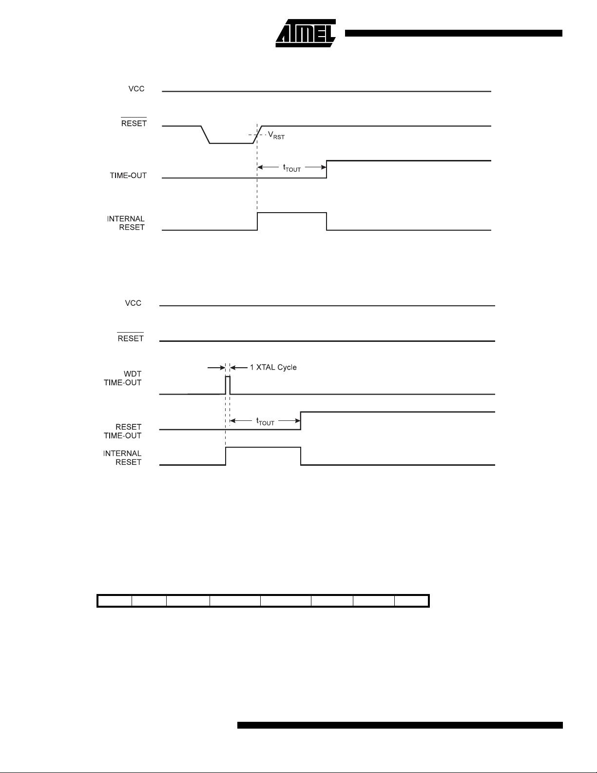
Figure 29.
External Reset During Operation
Watchdog Reset
When the Watchdog times out, it will generate a short reset
pulse of 1 XTAL cycle duration. On the falling edge of this
Figure 30.
Watchdog Reset During Operation
Interrupt Handling
The AT90S8515 has two 8-bit In terrupt M ask contr ol regi sters; GIMSK - General Interrupt Mask register and TIMSK Timer/Counter Interrupt Mask register.
When an interrupt occurs, the Global Interrupt Enable I-bit
is cleared (zero) and all inter rupts are dis abled. The us er
software must set (one) the I-bit to enable interrupts.
The General Interrupt Mask Register - GIMSK
pulse, the delay tim er starts counting the Time-out period
. Refer to page 30 for details on operation of the
t
TOU T
Watchdog.
When the Program Counter is vectored to the actual interrupt vector in order to execute the interrupt handling routine, hardware clears the corresponding flag that generated
the interrupt. Some of the interrupt flags can also be
cleared by writing a logic one to the flag bit position(s) to be
cleared.
Bit 7 6 5 4 3 2 1 0
$3B ($5B)
Read/Write R/W R/W R R R R R R
Initial value 0 0 0 0 0 0 0 0
Bit 7 - INT1: External Interrupt Request 1 Enable
•
When the INT1 bit is set (one) and the I-bit in the Status
Register (SREG) is set (one), the external pin interrupt is
activated. The Interrupt Sense Control1 bits 1/0 (ISC11 and
ISC10) in the MCU general Control Register (MCUCR)
INT1 INT0 - - - - - - GIMSK
or falling edge of the INT1 pin or level sensed. Ac tivity on
the pin will cause an interrupt request even if INT1 is configured as an ou tput. The corre spond ing int errupt of External Interrupt Request 1 is executed from program memory
address $002. See also “External Interrupts”.
defines whether the exter nal int err upt is acti vated on risin g
18
AT90S8515
Bit 6 - INT0: External Interrupt Request 0 Enable
•
When the INT0 bit is set (one) and the I-bit in the Status
Register (SREG) is set (one), the external pin interrupt is
activated. The Interrupt Sense Control0 bits 1/0 (ISC01 and
ISC00) in the MCU general Control Register (MCUCR)
defines whether the exter nal int err upt is acti vated on risin g
figured as an ou tput. The corre spond ing int errupt of External Interrupt Request 0 is executed from program memory
address $001. See also “External Interrupts.”
Bits 5..0 - Res: Reserved bits
•
These bits are reserved bits in the A T90S 8515 a nd always
read as zero.
or falling edge of the INT0 pin or level sense d. Activity on
the pin will cause an interrupt request even if INT0 is con-
The General Interrupt Flag Register - GIFR
Bit 7 6 5 4 3 2 1 0
$3A ($5A)
Read/Write R/W R/W R R R R R R
Initial value 0 0 0 0 0 0 0 0
Bit 7 - INTF1: External Interrupt Flag1
•
When an event on the IN T1 pin triggers an interr upt
request, INTF1 becomes set (one). If the I-bit in SREG and
the INT1 bit in GIMSK are set (one), the MCU will jump to
the interrupt vector at address $002. The fl ag is clea red
when the interrupt routine is executed. Alternatively, the
flag can be cleared by writing a logical one to it.
Bit 6 - INTF0: External Interrupt Flag0
•
INTF1 INTF0 - - - - - - GIFR
the INT0 bit in GIMSK are set (one), the MCU will jump to
the interrupt vector at address $001. The f lag is cl eared
when the interrupt routine is executed. Alter natively, the
flag can be cleared by writing a logical one to it.
Bits 5..0 - Res: Reserved bits
•
These bits are reserved bits in the A T90S 8515 a nd always
read as zero.
When an event on the IN T0 pin triggers an interr upt
request, INTF0 becomes set (one). If the I-bit in SREG and
The Timer/counter Interrupt Mask Register - TIMSK
Bit 7 6 5 4 3 2 1 0
$39 ($59)
Read/Write R/W R/W R/W R R/W R R/W R
Initial value 0 0 0 0 0 0 0 0
Bit 7 - TOIE1: Timer/Counter1 Overflow Interrupt Enable
•
When the TOIE1 bit is set (one) and the I-bit in the Status
Register is set (one), the Timer/Counter1 Overflow interrupt
is enabled. The corresponding interrupt (at vector $006) is
executed if an overflo w in Timer/Counter1 occ urs. The
Overflow Flag (Timer/Counter1) is set (one) in the
Timer/Counter Interrupt Flag Register - TIFR. When
Timer/Counter1 is in PWM mode, the Timer Over flow flag
is set when the counter changes counting direction at
$0000.
Bit 6 - OCE1A:Timer/Counter1 Output CompareA Match
•
Interrupt Enable
When the OCIE1A bit is set (one) and the I-bit in the Status
Register is set (one), the Timer/Counter1 CompareA Match
interrupt is enabled. The corresponding interrupt (at vector
$004) is executed if a Compa reA matc h in Timer/Cou nter1
occurs. The Compare A Flag in Tim er /Cou nter1 is s et (o ne)
in the Timer/Counter Interrupt Flag Register - TIFR.
Bit 5 - OCIE1B:Timer/Counter1 Output CompareB Match
•
Interrupt Enable
When the OCIE1B bit is set (one) and the I-bit in the Status
Register is set (one), the Timer/Counter1 CompareB Match
interrupt is enabled. The corresponding interrupt (at vector
TOIE1 OCIE1A OCIE1B - TICIE1 - TOIE0 - TIMSK
occurs. The CompareB Flag in Timer/Counter1 is set (o ne)
in the Timer/Counter Interrupt Flag Register - TIFR.
Bit 4 - Res: Reserved bit
•
This bit is a reserved bit in the AT90S8515 and always
reads zero.
Bit 3 - TICIE1: Timer/Counter1 Input Capture Interrupt
•
Enable
When the TICIE1 bit is set (one) an d the I-b it in the S tatus
Register is set (one), the Timer/Counter1 Input Capture
Event Interrupt is enabled. The corresponding interrupt (at
vector $003) is executed if a capture-triggering event
occurs on pin 31, ICP. The Input Capture Flag i n
Timer/Counter1 is set (one) in the Timer/Counter Interrupt
Flag Register - TIFR.
Bit 2 - Res: Reserved bit
•
This bit is a reserved bit in the AT90S8515 and always
reads zero.
Bit 1 - TOIE0: Timer/Counter0 Overflow Interrupt Enable
•
When the TOIE0 bit is set (one) and the I-bit in the Status
Register is set (one), the Timer/Counter0 Overflow interrupt
is enabled. The corresponding interrupt (at vector $008) is
executed if an overflow in Timer/Counter0 occur s. The
$005) is executed if a Compa reB matc h in Timer/Cou nter1
AT90S8515
19

Bit 0 - Res: Reserved bit
Overflow Flag (Timer0) is set (one) in the Timer/Counter
Interrupt Flag Register - TIFR.
•
This bit is a reserved bit in the AT90S8515 and always
reads zero.
The Timer/Counter Interrupt Flag Register - TIFR
Bit 7 6 5 4 3 2 1 0
$38 ($58)
Read/Write R/W R/W R/W R R/W R R/W R
Initial value 0 0 0 0 0 0 0 0
Bit 7 - TOV1: Timer/Counter1 Overflow Flag
•
The TOV1 is set (one) when an overflow occurs in
Timer/Counter1. TOV1 is cleared b y hardware when executing the cor resp ond ing interrupt hand li ng vector. Alternatively, TOV1 is cleared by writing a logic one to the flag.
When the I-bit in SREG, and TOIE1 (Timer/Counter1 Overflow Interrupt Enable), and TOV1 are set (one), the
Timer/Counter1 Overflow In terrupt is executed. In PWM
mode, this bit is set when Timer/Counter1 changes counting direction at $0000.
Bit 6 - OCF1A: Output Compare Flag 1A
•
The OCF1A bit is set (one) when compare match occurs
between the Timer/Counter1 and the data in OCR1A - Output Compare Register 1A. OCF1A is cleared by hardware
when executing the corresponding interrupt handling vector. Alternatively, OCF1A is cleared by writing a logic one to
the flag. When the I-bit in SREG, and OCIE1A
(Timer/Counter1 Comp are match Interrup tA Enable), an d
the OCF1A are set (one), the Timer/Counter1 Compare
match Interrupt is executed.
Bit 5 - OCF1B: Output Compare Flag 1B
•
The OCF1B bit is set (one) when compare match occurs
between the Timer/Counter1 and the data in OCR1B - Output Compare Register 1B. OCF1B is cleared by hardware
when executing the corresponding interrupt handling vector. Alternatively, OCF1B is cleared by writing a logic one to
the flag.. When the I-bit in SREG, and OCIE1B
(Timer/Counter1 Comp are match Interrup tB Enable), an d
the OCF1B are set (one), the Timer/Counter1 Compare
match Interrupt is executed.
Bit 4 - Res: Reserved bit
•
This bit is a reserved bit in the AT90S8515 and always
reads zero.
Bit 3 - ICF1: - Input Capture Flag 1
•
The ICF1 bit is set (one) to flag an input capture event, indicating that the Timer/Counter1 value has been transferred
to the input capture register - ICR1. ICF 1 is cleared by
hardware when ex ecutin g the cor respo nding int errupt handling vector. Alternatively, ICF1 is cleared by writing a logic
one to the flag.
Bit 2 - Res: Reserved bit
•
This bit is a reserved bit in the AT90S8515 and always
reads zero.
TOV1 OCF1A OCIFB - ICF1 - TOV0 - TIFR
Bit 1 - TOV: Timer/Counter0 Overflow Flag
•
The bit TOV0 is set (one) when an ov erflow occurs in
Timer/Counter0. TOV0 is cleared b y hardware when executing the corresp ond ing i nte rrup t h and li ng v ect or. A lt er natively, TOV0 is cleared by writing a logic one to the flag.
When the SREG I-bit, and TOIE0 (Timer/Counter0 Overflow Interrupt Enable), and TOV0 are set (one), the
Timer/Counter0 Overflow interrupt is executed.
Bit 0 - Res: Reserved bit
•
This bit is a reserved bit in the AT90S8515 and always
reads zero.
External Interrupts
The external interrupts are triggered by the INT1 and INT0
pins. Observe that, if enabled, the interrupts will trigger
even if the INT0/INT1 pins are configured as outputs. This
feature provides a way of gen erating a s oftware interrupt.
The external interrupts can be triggered by a falling or rising edge or a low level. This is set up as indicated in the
specification for the MCU Control Register - MCUCR.
When the external interrupt is enabled and is configured as
level triggered, the interrupt will trigger as long as the pin is
held low.
The external interrupts are set up as described in the specification for the MCU Control Register - MCUCR.
Interrupt Response Time
The interrupt execu tion respons e for all the enable d
interrupts is 4 clock cycles minimum. 4 clock cycles after
the interrupt flag has be en s et, the program vector address
for the actual interrupt han dling routine is exec uted. Durin g
this 4 clock cycle period, the Program Counter (2 bytes) is
pushed onto the Stack, and the Stack Pointer is decremented by 2. The vector is a relative jump to the interrupt
routine, and this jump takes 2 clock cycles. If an interrupt
occurs during execution of a multi-cycle i nstructio n, this
instruction is completed before the interrupt is served.
A return from an interrupt hand ling routi ne (same as for a
subroutine call routine) takes 4 clock cycles. During these 4
clock cycles, the Program Counter (2 bytes) is popped
back from the Sta ck, and th e Stack Point er is inc remente d
by 2. When the AVR exits fro m an interrupt, it will always
return to the main program and execute one more instruction before any pending interrupt is served.
Note that th e Status Regi ster - SREG - is n ot han dled by
the AVR hardware, neither for interrupts nor for subrou-
AVR
20
AT90S8515
AT90S8515
tines. For the interrupt handling routines requiring a storage
of the SREG, this must be performed by user software.
For Interrupts trigger ed by events that can remai n static
(E.g. the Output Compare Register1 A matching the value
of Timer/Counter1) the interrupt flag is set when the event
occurs. If the interrupt fla g is c leared an d the int errupt c ondition persists, the fla g wil l n ot be se t unti l t he ev en t occu rs
the next time.
MCU Control Register - MCUCR
The MCU Control Register contains control bits for general MCU functions.
Bit 76543210
$35 ($55)
Read/Write R/W R/W R/W R/W R/W R/W R/W R/W
Initial value 0 0 0 0 0 0 0 0
Bit 7 - SRE: External SRAM Enable
•
When the SRE bit is set (one), the external data SRAM is
enabled, and the pin functions AD0 -7 (P ort A) , A8-15 (P ort
C), WR
and RD (Port D) are activated as the alternate pin
functions. Then the SRE bit overrides any pin direction settings in the respective data direction registers. See “The
SRAM Data Memory - Internal and External” for description
of the External SRAM pin functions. When the SRE bit is
cleared (zero), the external data SRAM is disabled, and the
normal pin and data direction settings are used.
Bit 6 - SRW: External SRAM Wait State
•
When the SRW bit is set (one), a one cy cle wait state is
inserted in the external data SRAM access cycle. When the
SRW bit is cl eared ( zero) , the exte rnal data S RAM ac cess
is executed with the normal three-cycle scheme. See Figure 23: External Data SRAM Memory Cycles without Wait
State and Figure 24: External Data SRAM Memory Cycles
with Wait State.
Bit 5 - SE: Sleep Enable
•
The SE bit must be set (one) to make the MCU enter the
sleep mode when the SLEEP instruction is executed. To
avoid the MCU entering the sleep mode unless it is the programmers purpose, it is recommended to set the Sleep
Enable SE bit just befor e the execution of the SLEEP
instruction.
Bit 4 - SM: Sleep Mode
•
This bit selects be tween the two av ailable sleep modes.
When SM is cleared (zero) , Idle Mode is sele cted as Slee p
Mode. When SM is set (one), Power Down mode is
selected as sleep mode. For details, r efer to the par agrap h
“Sleep Modes” below.
Bit 3, 2 - ISC11, ISC10: Interrupt Sense Control 1 bit 1 and
•
bit 0
The External Interrupt 1 is activated by the external pin
INT1 if the SR EG I-flag and the corre spondin g interrup t
mask in the GIMSK is set. The level and edges on the
SRE SRW SE SM ISC11 ISC10 ISC01 ISC00 MCUCR
external INT1 pin that activ ate the interru pt are defined i n
the following table:
Table 4.
ISC11 ISC10 Description
Note: When changing the ISC11/ISC10 bits, INT1 must be dis-
Interrupt 1 Sense Control
00
01Reserved
10
11
abled by clearing its Interrupt Enable bit in the GIMSK
Register. Otherwise an inte rrupt can oc cu r w hen the bits
are changed.
The low level of INT1 generates an
interrupt request.
The falling edge of INT1 generates an
interrupt request.
The rising edge of INT1 generates an
interrupt request.
• Bit 1, 0 - ISC01, ISC00: Interrupt Sense Control 0 bit 1 and
bit 0
The External Interrupt 0 is activated by the external pin
INT0 if the SREG I-flag and the corresponding interrupt
mask is set. The level and edges on the external INT0 pin
that activate the interrupt are defined in the following table:
Table 5.
ISC01 ISC00 Description
Note: When changing the ISC10/ISC00 bits, INT0 must be dis-
Interrupt 0 Sense Control
00
01Reserved
10
11
abled by clearing its Interrupt Enable bit in the GIMSK
Register. Otherwise an inte rrupt can oc cu r w hen the bits
are changed.
The low level of INT0 generates an
interrupt request.
The falling edge of INT0 generates an
interrupt request.
The rising edge of INT0 generates an
interrupt request.
21
Sleep Modes
To enter the sleep modes, the SE bit in MCUCR must be
set (one) and a SLEEP instruction must be executed. If an
enabled interrupt occurs while the MCU is in a sleep mode,
the MCU awakes, executes the interrupt routine, and
resumes execution from the instruction following SLEEP.
The contents of the register file, SRAM and I/O memory are
unaltered. If a reset occurs during sleep mode, the MCU
wakes up and executes from the Reset vector.
Idle Mode
When the SM bit is cleared (zero), the SLEEP instruction
forces the MCU into the Idle Mode stopping the CPU but
allowing Timer/Counters, Watchdog and the interrupt system to continue operating. This enables the MCU to wake
up from external triggered interrupts as well as internal
ones like Timer Overflow interrupt and watchdog reset. If
wakeup from the Analog Comparator interrupt is not
required, the analog comparator can be powered down by
setting the ACD-bit in the Analog Comparator Control and
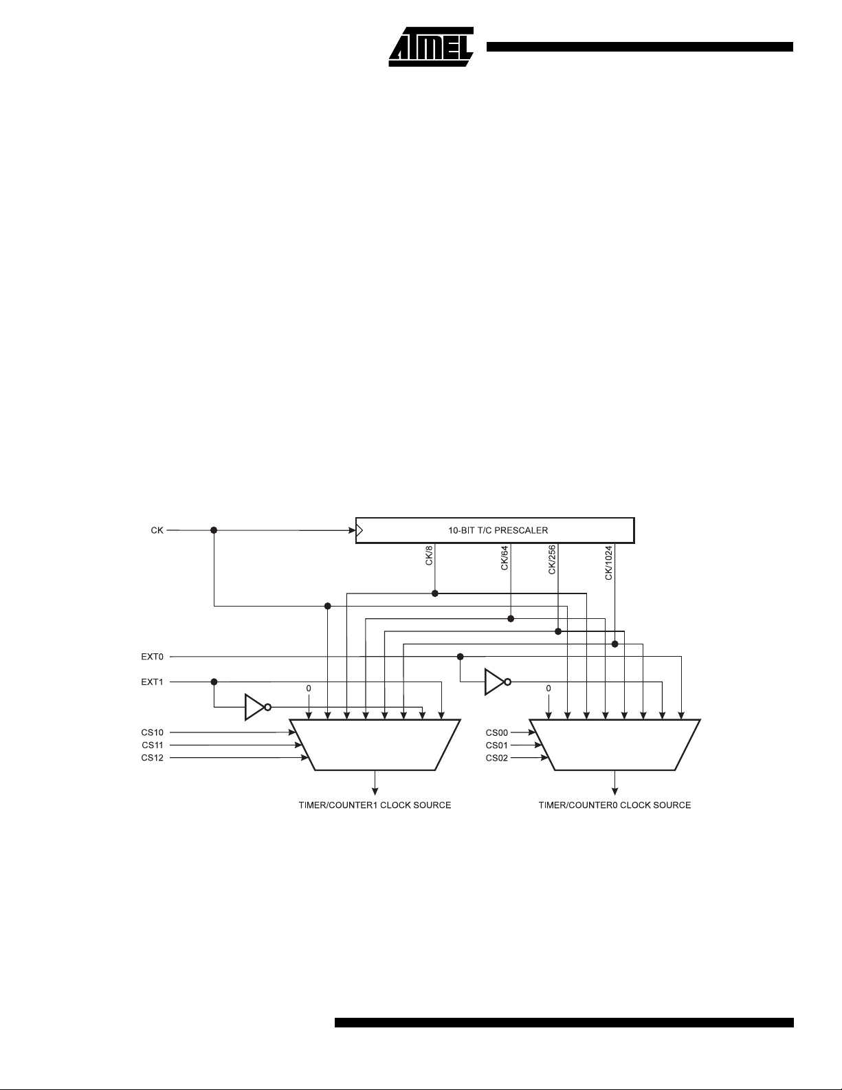
The Timer/Counter Prescaler
Figure 31 shows the general Timer/Counter prescaler.
Status register - ACSR. Thi s will reduce power consumption in Idle Mode.
Power Down Mode
When the SM bit is set (one ), the S LEEP in struc tion fo rces
the MCU into the Power Down Mode. In this mode, the
external oscillator is stopped. The user can select whether
the watchdog shall be enabled during power-down mode. If
the watchdog is enabled, it will wake up the MCU when the
Watchdog Time-out period expires. If the watchdog is disabled, only an external reset or an external level triggered
interrupt can wake up the MCU.
Timer / Counters
The AT90S8515 provides two general purpose
Timer/Counters - one 8-bit T/C and one 16-bit T/C . The
Timer/Counters have individual prescaling selection from
the same 10-bit prescali ng timer. Both Tim er/Counte rs can
either be used as a timer with an internal clock tim ebas e or
as a counter with an external pin connecti on which tri ggers
the counting.
Figure 31.
The four different prescaled selections are: CK/8, CK/64,
CK/256 and CK/1024 where CK is the oscillator clock. For
the two Timer/Counters, added selections as CK, external
source and stop, can be selected as clock sources.
Timer/Counter Prescaler
22
AT90S8515
The 8-Bit Timer/Counter0
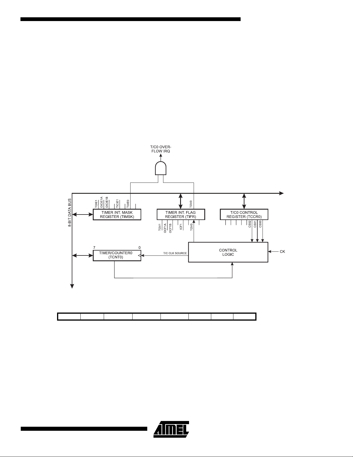
Figure 32 shows the block diagram for Timer/Counter0.
The 8-bit Timer/Counter 0 ca n s elec t c lock s ourc e fr om CK ,
prescaled CK, or an external pin. In addition it can be
stopped as described in the specification for the
Timer/Counter0 Control Register - TCCR0. The overflow
status flag is foun d in the Timer/Co unter Insterrup t Flag
Register - TIFR. Control sign als are found in the
Timer/Counter0 Control Register - TCCR0. The interrupt
enable/disable settings for Timer/Counter0 are found in the
Timer/Counter Interrupt Mask Register - TIMSK.
AT90S8515
When Timer/Counter0 is externally clocked, the external
signal is synch ronized wi th the o scillator frequenc y of the
CPU. To assure proper sampling of the external clock, the
minimum time between two external clock transitions must
be at least one internal CPU clock period. The external
clock signal is sampled on the rising edge of the internal
CPU clock.
The 8-bit Timer/Counter0 features both a high resolution
and a high accuracy usage with the lower prescaling opportunities. Simila rly, the hi gh prescali ng opportun ities ma ke
the Timer/Counter0 useful for lower spe ed functions or
exact timing functions with infrequent actions.
Figure 32.
Timer/Counter0 Block Diagram
The Timer/Counter0 Control Register - TCCR0
Bit 7 6 5 4 3 2 1 0
$33 ($53)
Read/Write R R R R R R/W R/W R/W
Initial value 0 0 0 0 0 0 0 0
Bits 7,6 - Res: Reserved bits
•
- - - - - CS02 CS01 CS00 TCCR0
These bits are reserved bits i n the A T90S85 15 and a lways
read zero.
Bits 2,1,0 - CS02, CS01, CS00: Clock Select0, bit 2,1 and 0
•
The Clock Select0 bits 2,1 and 0 define the prescaling
source of Timer0.
23

Table 6.
Clock 0 Prescale Select
CS02 CS01 CS00 Description
0 0 0 Stop, the Timer/Counter0 is stopped.
001CK
010CK / 8
011CK / 64
100CK / 256
101CK / 1024
1 1 0 External Pin T0, falling edge
1 1 1 External Pin T0, rising edge
The Stop condition provides a Timer Enable/Disable function. The CK down divided modes are scaled directly from
the CK oscilla tor cl ock. I f t he exter nal pin mo de s are used ,
the corresponding setup must be performed in the actual
data direction control register (cleared to zero gives an
input pin).
The Timer Counter 0 - TCNT0
Bit 76543210
$32 ($52)
Read/Write R/W R/W R/W R/W R/W R/W R/W R/W
Initial value 0 0 0 0 0 0 0 0
MSB LSB TCNT0
The Timer/Counter0 is realized as an up-counter with read
and write access. If the T imer/Counter0 is wr itten and a
clock source is present, the Timer/Counter0 continues
counting in the clock cycle following the write operation.
24
AT90S8515

The 16-Bit Timer/Counter1
Figure 33 shows the block diagram for Timer/Counter1.
AT90S8515
Figure 33.
Timer/Counter1 Block Diagram
The 16-bit Timer/Co unter1 can sele ct clock source from
CK, prescaled CK, or an external pin. In addition it can be
stopped as described in the specification for the
Timer/Counter1 Control Registers - TCCR1A and
TCCR1B. The different status flags (overflow, compare
match and capture event) and control signals are found in
the Timer/Counter1 Control Registers - TCCR1A and
TCCR1B. The interrupt enable/disable settings for
Timer/Counter1 are found in the Timer/Counter Interrupt
Mask Register - TIMSK.
When Timer/Counter1 is externally clocked, the external
signal is synchro nized wi th the o scillator frequency of the
CPU. To assure proper sampling of the external clock, the
minimum time between two external clock transitions must
be at least one internal CPU clock period. The external
clock signal is sampled on the rising edge of the internal
CPU clock.
The 16-bit Timer/Counter1 features both a high resolution
and a high accuracy usage with the lower prescaling oppor-
tunities. Similarly, the high prescaling opportunities makes
the Timer/Counter1 useful for lower spe ed functions or
exact timing functions with infrequent actions.
The Timer/Counter1 supports two Output Compare functions using the Output Compare R egister 1 A and B OCR1A and OCR1B as the dat a sources to be compar ed
to the Timer/Counter1 contents. The Output Compare functions include optional clearing of the counter on compareA
match, and actions on the Output Compare pins on both
compare matches.
Timer/Counte r1 ca n also be used as a 8, 9 or 10 -bit Pulse
With Modulator. In this mode the counter and the
OCR1A/OCR1B registe rs se rv e a s a du al gl it ch -fr ee sta ndalone PWM with centered pulses. Refer to page 33 for a
detailed description on this function.
The Input Capture function of Timer/Counter1 provides a
capture of the Timer/Counter1 contents to the Input Capture Register - ICR1, triggere d by an ex ternal ev ent on the
Input Capture Pin - ICP. The actual capture event settings
25

are defined by the Timer/Counter1 Control Register TCCR1B. In addition, the Analog Comparator ca n be set to
trigger the Input Capture. Refer to the section, “The Analog
Comparator”, for details on this. The ICP pin logic is shown
in Figure 34.
Figure 34.
If the noise canceler function is enabled, the actual trigger
condition for the capture event is monitored over 4 samples
ICP Pin Schematic Diagram
before the capture is activated. The input pin signal is sampled at XTAL clock frequenc y.
The Timer/Counter1 Control Register A - TCCR1A
Bit 7 6 5 4 3 2 1 0
$2F ($4F)
Read/Write R/W R/W R/W R/W R R R/W R/W
Initial value 0 0 0 0 0 0 0 0
Bits 7,6 - COM1A1, COM1A0: Compare Output Mode1A,
•
bits 1 and 0
The COM1A1 and COM1A0 control bits determine any output pin action following a compare match in
Timer/Counter1. Any output pin actions affect pin OC1A Output CompareA pin 1. Since this is an alternative function to an I/O port, the corresponding direction control bit
must be set (one) to con tr ol a n ou tput p in . The c ontr ol c onfiguration is shown in Table 7.
Bits 5,4 - COM1B1, COM1B0: Compare Output Mode1B,
•
bits 1 and 0
The COM1B1 and COM1B0 control bits determine any output pin action following a compare match in
Timer/Counter1. Any output pin actions affect pin OC1B Output CompareB. The following con trol configuration is
given:
Table 7.
COM1X1 COM1X0 Description
00
0 1 Toggle t he OC1X output line.
COM1A1 COM1A0 COM1B1 COM1B0 - - PWM11 PWM10 TCCR1A
rupt Enable bits in the TIMSK Regist er. Otherwise an
interrupt can occur when the bits are changed.
Bits 3..2 - Res: Reserved bits
•
These bits are reserved bits in the A T90S 8515 a nd always
read zero.
Bits 1..0 - PWM11, PWM10: Pulse Width Modulator Select
•
Bits
These bits select PWM operation of Timer/Counter1 as
specified in Table 8. This mode is described on page 29.
Table 8.
PWM11 PWM10 Description
Compare 1 Mode Select
Timer/Counter1 disconnected from
output pin OC1X
PWM Mode Select
00
0 1 Timer/Counter1 is an 8-bit PWM
1 0 Timer/Counter1 is a 9-bit PWM
1 1 Timer/Counter1 is a 10-bit PWM
PWM operation of Timer/Counter1 is
disabled
1 0 Clear the OC1X output line (to zero).
1 1 Set the OC1X output line (to one).
X = A or B
In PWM mode, these bits have a different function. Refer to
Table 11 for a detailed description.
When changing the COM1X1/COM1X0 bits, Ou tput Compare Interrupts 1 must be disab led by cleari ng thei r Inter-
26
AT90S8515

The Timer/Counter1 Control Register B - TCCR1B
Bit 7 6 5 4 3 2 1 0
$2E ($4E)
Read/Write R/W R/W R R R/W R/W R/W R/W
Initial value 0 0 0 0 0 0 0 0
•
Bit 7 - ICNC1: Input Capture1 Noise Canceler (4 CKs)
When the ICNC1 bit is cleared (zero), the input capture trigger noise canceler function is disabled. The input capture is
triggered at the first rising/falling edge sampled on the ICP input capture pin - as specified. When the ICNC1 bit is set
(one), four successive samples are measures on the ICP input capture pin, and all samples must be high/low according to the input capture trigger specification in the ICES1
bit. The actual sam pling frequency is XTAL clock frequency.
Bit 6 - ICES1: Input Capture1 Edge Select
•
While the ICES1 bit is cleared (zero), the Timer/Counter1
contents are transferred to the Input Capture Register ICR1 - on the falling edge of the input capture pin - ICP.
While the ICES1 bit is set (one), the T imer/Counter1 c ontents are transferred to the Input Captur e Register - ICR1 on the rising edge of the input capture pin - ICP.
Bits 5, 4 - Res: Reserved bits
•
These bits are reserved bits i n the A T90S85 15 and a lways
read zero.
Bit 3 - CTC1: Clear Timer/Counter1 on Compare Match
•
When the CTC1 control bit is set (one), the Timer/Counter1
is reset to $0000 in the clock cycle after a compareA
match. If the CTC1 control bit is cleared, Timer/Counter1
ICNC1 ICES1 - - CTC1 CS12 CS11 CS10 TCCR1B
... | C-1 | C | C+1 | 0 | 1 | ...
When the prescaler is set to divide by 8, the timer will count
like this:
... | C-1, C-1, C-1, C-1, C-1, C-1, C-1, C-1 | C, C, C, C, C,
C, C, C | C+1, 0, 0, 0, 0, 0, 0, 0, 0 | ...
In PWM mode, this bit has no effect.
Bits 2,1,0 - CS12, CS11, CS10: Clock Select1, bit 2,1 and 0
•
The Clock Select1 bits 2,1 and 0 define the prescaling
source of Timer/Counter1.
Table 9.
CS12 CS11 CS10 Description
Clock 1 Prescale Select
0 0 0 Stop, the Timer/Counter1 is stopped.
001CK
0 1 0 CK / 8
011CK / 64
1 0 0 CK / 256
1 0 1 CK / 1024
1 1 0 External Pin T1, falling edge
1 1 1 External Pin T1, rising edge
continues count ing and is un affected by a compar e match.
Since the compare match is detected in the CPU cl ock
cycle following the match, this function will behave differently when a prescaling hi gher than 1 is used fo r the timer .
When a prescaling o f 1 is u sed , an d the co mpa re A r eg ist er
is set to C, the timer will count as follows i CTC1 is set:
The Stop condition provides a Timer Enable/Disable function. The CK down divided modes are scaled directly from
the CK oscilla tor cl ock. If t he ex ternal pin mode s are used ,
the corresponding setup must be performed in the actual
direction control register (cleared to zero gives an input
pin).
The Timer/Counter1 - TCNT1H AND TCNT1L
AT90S8515
Bit 151413121110 9 8
$2D ($4D)
$2C ($4C)
Read/Write R/W R/W R/W R/W R/W R/W R/W R/W
Initial value 0 0 0 0 0 0 0 0
This 16-bit regis ter cont ains th e prescale d valu e of the 16bit Timer/Counter1. To ensure that both the high and low
bytes are read and wri tten sim ultaneous ly when the CP U
accesses these registers, the access is performed using an
8-bit temporary register ( TEMP). This temporary register is
also used when accessing OCR1A, OCR1B and ICR1. If
the main program and also interrupt routines perform
MSB TCNT1H
LSB TCNT1L
76543210
R/W R/W R/W R/W R/W R/W R/W R/W
00000000
access to regi sters using TEMP, interr upts must be disabled during access from the main program.
• TCNT1 Timer/Counter1 Write:
When the CPU writes to the high byte TCNT1H, the
written data is placed in the TEMP register. Next, when
the CPU writes the low byte TCNT1L, this byte of data
is combined with the byte data in the TEMP register,
27

and all 16 bits are written to the TCNT1
Timer/Counter1 register simultaneously. Consequently, the high byte TCNT1H must b e accessed firs t
for a full 16-bit register write operation.
• TCNT1 Timer/Counter1 Read:
When the CPU reads the low byte TCNT1L, the data of
the low byte TCNT1L is sent to the CPU and the data of
the high byte TCNT1H is placed in th e TEMP register.
TCNT1H, the CPU receives the data in th e TEMP register. Consequently, the low byte TCNT1L must be
accessed first for a full 16-bit register read operation.
The Timer/Coun ter1 is real ized as an up or u p/down (in
PWM mode) counter with read and write access. If
Timer/Counter1 is written to and a clock source is selected,
the Timer/Counter1 continues counting in the timer clock
cycle after it is preset with the written value.
When the CPU reads the data in the high byte
Timer/Counter1 Output Compare Register - OCR1AH AND OCR1AL
Bit 151413121110 9 8
$2B ($4B)
$2A ($4A)
Read/Write R/W R/W R/W R/ W R/W R/W R/W R/W
Initial value 0 0 0 0 0 0 0 0
MSB OCR1AH
LSB OCR1AL
76543210
R/W R/W R/W R/W R/W R/W R/W R/W
00000000
Timer/Counter1 Output Compare Register - OCR1BH AND OCR1BL
Bit 151413121110 9 8
$29 ($49)
$28 ($48)
Read/Write R/W R/W R/W R/W R/W R/W R/W R/W
Initial value 0 0 0 0 0 0 0 0
MSB OCR1BH
LSB OCR1BL
76543210
R/W R/W R/W R/W R/W R/W R/W R/W
00000000
The output compare registers are 16-bit read/write registers.
The Timer/Counter1 Output Compare Registers contain
the data to be continuously compared with Timer/Counter1.
Actions on compare matc hes are specified in the
Timer/Counter1 Control and Status register.A compare
match does only occur if Tim er/Counter1 coun ts to the
OCR value. A so ftwar e wri te th at s ets TCN T1 and OC R1A
or OCR1B to the same value does not generate a compare
match.
A compare match will set the compare interrupt flag in the
CPU clock cycle following the compare event.
Since the Out put Compare Registers - OCR1A and
OCR1B - are 16-bit registers, a temporary register TEMP is
used when OCR1A/B are written to ensure that both bytes
are updated simultaneously. When the CPU writes the high
byte, OCR1AH or OCR1BH, the data is temporarily stored
in the TEMP register. When the CPU writes the low byte ,
OCR1AL or OCR1BL, the TEMP register is simultaneously
written to OCR1AH or OCR1BH. Consequently, the high
byte OCR1AH or OCR1BH must be written first for a full
16-bit register write operation.
The TEMP register is also used when accessing TCNT1,
and ICR1. If the main program and also interrupt ro utines
perform access to registers using TEMP, interrupts must
be disabled during access from the main program.
28
AT90S8515

AT90S8515
The Timer/Counter1 Input Capture Register - ICR1H AND ICR1L
Bit 151413121110 9 8
$25 ($45)
$24 ($44)
Read/Write RRRRRRRR
Initial value 0 0 0 0 0 0 0 0
MSB ICR1H
LSB ICR1L
76543210
RRRRRRRR
00000000
The input capture register is a 16-bit read-only register.
When the rising or falling e dge (a ccordi ng to the i nput c ap-
ture edge setting - ICES1) of the sign al at the input capt ure
pin - ICP - is detected, the current value of the
Timer/Counter1 is transferred to the Input Capture Register
- ICR1. At the same time, the input capture flag - ICF1 - is
set (one).
Since the Input Cap ture Re giste r - ICR1 - is a 16 -bit reg ister, a temporary register TEMP is used when ICR1 is read
to ensure that both bytes are read simultaneously. When
the CPU reads the low byte ICR1L, the data is sent to the
CPU and the data of the high byte ICR1H is placed in the
TEMP register. When the CPU reads the data in the high
byte ICR1H, the CPU receives the data in the TEMP register. Consequent ly, the low byte ICR 1L must be acce ssed
first for a full 16-bit register read operation.
The TEMP regi ster is a lso used wh en acces sing TCNT 1,
OCR1A and OCR1B. If the main program and also interrupt
routines perform access to registers using TEMP, interrupts must be disabled during access from the main program.
Timer/Counter1 In PWM Mode
When the PWM mode is selected, Timer /Counter1 and the
Output Compare Register1A - OCR1A and the Output
Compare Register1B - OCR1B, form a dual 8, 9 or 10-bit,
free-running, glitch-free and phase correct PW M with outputs on the PD5(OC1A) and OC1B pins. Timer/Counter1
acts as an up/down counter, counting up from $0000 to
TOP (see Table 10) , whe n it turns a nd cou nts down ag ain
to zero before the cycle is repeated. When the counter
value matches the contents of the 10 least significan t bits
of OCR1A or OCR1B, the PD5(OC1A)/OC1B pins are set
or cleared according to the settings of the
COM1A1/COM1A0 or C OM1B1/COM1B0 bits in th e
Timer/Counter1 Control Register TCCR1A. Refer to Table
11 for details.
Table 10.
Timer TOP Values and PWM Frequency
Table 11.
COM1X1 COM1X0 Effect on OCX1
Note: X = A or B
Compare1 Mode Select in PWM Mode
0 0 Not connected
0 1 Not connected
Cleared on compare match,
10
11
upcounting. Set on compare match,
downcounting (non-inverted PWM).
Cleared on compare match,
downcounting. Set on compare
match, upcounting (inverted PWM).
Note that in the PWM mode, the 10 least significant
OCR1A/OCR1B bits, when written, are transferred to a
temporary location. They are latched when Timer/Counter1
reaches the value TOP. This prevents the oc currence of
odd-length PWM pulses (glitches) in the event of an unsynchronized OCR1A/OCR1B write. See Figure 35 for an
example.
PWM Resolution Timer TOP value Frequency
8-bit $00FF (255) f
9-bit $01FF (511) f
10-bit $03FF(1023) f
TC1
TC1
TC1
/510
/1022
/2046
29

Figure 35.
Effects on Unsynchronized OCR1 Latching
During the time between the write and the latch operation,
a read from OCR1A or OCR1B will read the contents of the
temporary location. This means that the mo st recen tly wr itten value always will read out of OCR1A/B
When OCR1 contains $0000 or TOP, the output
OC1A/OC1B is held low or high according to the settings of
COM1A1/COM1A0 or COM1B1/COM1B0. This is shown in
Table 12:
Table 12.
COM1X1 COM1X0 OCR1X Output OC1X
Note: X = A or B
In PWM mode, the Timer Overflow Flag1, T OV1, is set
when the counter change s directi on at $0000. Tim er Overflow Interrupt1 operates exactly as in normal Timer/Counter
mode, i.e. it is executed when TOV1 is set provided that
Timer Overflow Interrupt1 and global interrupts are
enabled. This does also apply to the Timer Output
Compare1 flags and interrupts.
PWM Outputs OCR1X = $0000 or TOP
1 0 $0000 L
10TOP H
1 1 $0000 H
11TOP L
cutes from the reset vector. For timing details on the
Watchdog reset, refer to page 18.
To prevent unintentional disabling of the watchdog, a special turn-off secuence must be followed when the watchdog
is disabled.Refer to the description of the Watchdog Timer
Control Register for details.
Figure 36.
Watchdog Timer
The Watchdog Timer
The Watchdog Timer is clocked from a separate on-chip
oscillator which runs at 1MHz This is the typical value at
= 5V. See characterization data for typical values at
V
CC
other V
caler, the Watchd og reset interva l can be adjusted fr om
16K to 2,048K cycles (nominally 16 - 2048 ms). The WDR Watchdog Reset - instruction resets the Watchdo g Timer.
Eight different clock cycle periods can be selected to determine the reset period. If the reset period expires without
another Watchdog reset, t he AT90S8515 resets and exe-
30
levels. By controlling the Watchdog Timer pres-
CC
AT90S8515

AT90S8515
The Watchdog Timer Control Register - WDTCR
Bit 76543210
$21 ($41)
Read/Write R R R R/W R/W R/W R/W R/W
Initial value 0 0 0 0 0 0 0 0
•
Bits 7..5 - Res: Reserved bits
These bits are reserved bits in the AT90S8515 and will
always read as zero.
Bit 4 - WDTOE: Watch Dog Turn-Off Enable
•
This bit must be set (one) when the WD E bit is clear ed.
Otherwise, the watchdo g will not be disabled. Onc e set,
hardware will clear this bit to zero after four clock cycles.
Refer to the desc ription of th e WDE bit for a watc hdog disable procedure.
Bit 3 - WDE: Watch Dog Enable
•
When the WDE is set (one) the Watchdog Timer is
enabled, and if the WDE is cleared (zero) the W atchdog
Timer function is disabled. WDE can only be cleared if the
WDTOE bit is set(one). To disable an enabled watchdog
timer, the following procedure must be followed:
1. In the same operation, write a logical one to
WDTOE and WDE. A logcal one must be written to
WDE even though it is set to one before the disable
operation starts.
2. Within the next four clock cycles, write a logical 0 to
WDE. This disables the watchdog.
Bits 2..0 - WDP2, WDP1, WDP0 : Watch Dog Timer Presc aler
•
2, 1 and 0
The WDP2, WDP1 and WDP0 bits determine the Watchdog Timer prescaling when the Watchdog Timer is
enabled. The different prescaling values and their corresponding Timeout Periods are shown in Table 13.
Table 13.
Watch Dog Timer Prescale Select
- - - WDTOE WDE WDP2 WDP1 WDP0 WDTCR
EEPROM Read/Write Access
The EEPROM access registers are accessible in the I/O
space.
The write access time is in the range of 2.5 - 4ms, depending on the V
lets the user softwar e detect when the ne xt byte can be
written. If the user code conta ins code that writes the
EEPROM, some precaution must be taken. In heavily filtered power suppl ies, V
power-up/down. This causes the device for some per iod of
time to run at a voltage lower than specified as minimum for
the clock frequency use d. CPU ope ration und er thes e conditions is likely ca use the prog ram co unter to perform uni ntentional jumps and even tually ex ecute the EEPROM write
code. To secure EEPROM integrity, the user is advised to
use an external under-voltage reset circuit in this case.
In order to prevent unintentional EEPROM writes, a specific write procedure must be followed. Refer to the description of the EEPROM Control Register for details on this.
When the EEPROM is read or written, the CPU is halted for
two clock cycles before the next instruction is executed.
voltages. A self-timing function, however,
CC
is likely to rise or fall slowly on
CC
WDP2 WDP1 WDP0 Timeout Period
0 0 0 16K cycles
0 0 1 32K cycles
0 1 0 64K cycles
0 1 1 128K cycles
1 0 0 256K cycles
1 0 1 512K cycles
1 1 0 1,024K cycles
1 1 1 2,048K cycles
31

The EEPROM Address Register - EEARH and EEARL
Bit 151413121110 9 8
$1F ($3F)
$1E ($3E)
Read/Write R/W R/W R/W R/ W R/W R/W R/W R/W
Initial value 8 0 0 0 0 0 0 0
- - - - - - - EEAR8 EEARH
EEAR7 EEAR6 EEAR5 EEAR4 EEAR3 EEAR2 EEAR1 EEAR0 EEARL
76543210
R/W R/W R/W R/W R/W R/W R/W R/W
80000000
The EEPROM Address Registers - EEARH and EEARL
specify the EEPROM address in the 512 bytes EEPROM
space. The EE PROM data by tes are addr essed line arly
between 0 and 512.
The EEPROM Data Register - EEDR
Bit 76543210
$1D ($3D)
Read/Write R/W R/W R/W R/W R/W R/W R/W R/W
Initial value 0 0 0 0 0 0 0 0
Bits 7..0 - EEDR7..0: EEPROM Data
•
For the EEPROM write operation, the EEDR register contains the data to be written to the EEPROM in the address
MSB LSB EEDR
given by the EEAR regi ster. For the EEPRO M read oper ation, the EEDR contains the data read out from the
EEPROM at the address given by EEAR.
The EEPROM Control Register - EECR
Bit 76543210
$1C ($3C)
Read/Write R R R R R R/W R/W R/W
Initial value 0 0 0 0 0 0 0 0
Bit 7..3 - Res: Reserved bits
•
These bits are reserved bits in the AT90S8515 and will
always read as zero.
Bit 2 - EEMWE: EEPROM Master Write Enable
•
The EEMWE bit determines whether setting EEWE to one
causes the EEPROM to be written. When EEMWE is
set(one) setting EEWE will write data to the EEPROM at
the selected address If EEMWE is zero, setting EEWE will
have no effect. When EEMWE has been set (one) by software, hardware clears the bit to zero after four clock cycles.
See the description of the EEWE bit for a EEPROM writ e
procedure.
Bit 1 - EEWE: EEPROM Write Enable
•
The EEPROM Write Enable Signal EE WE is the write
strobe to the EEPROM. When address and data are correctly set up, the EEWE bi t must be s et to write the v alue
into the EEPROM. The EEMWE bit must b e set when the
logical one is written to E EWE, otherwise no EEPROM
write takes place. The following procedure should be followed when writing the EE PROM (the orde r of st eps 2 and
3 is unessential):
1. Wait until EEWE becomes zero.
2. Write new EEPROM address to EEARL and
EEARH (optional)
- - - - - EEMWE EEWE EERE EECR
3. Write new EEPROM data to EEDR (optional)
4. Write a logical one to the EEMWE bit in EECR
5. Within four clock cycles after setting EEMWE, write
a logical one to EEWE.
When the write access time (typically 2.5 ms at V
4 ms at V
= 2.7V) has elapsed, the EEWE bit is cleared
CC
(zero) by hardware. The user software can poll this bit and
wait for a zero before writing the next byte. When EEWE
has been set, the CPU i s halted for two cyc les before th e
next instruction is executed.
Bit 0 - EERE: EEPROM Read Enable
•
The EEPROM Read Enable Signal EERE is the read
strobe to the EEPROM. When the correct address is set up
in the EEAR register, the EERE bit must be set. When the
EERE bit is cleared (zero) by hardware, requested data is
found in the EEDR register. The EEPROM read access
takes one instruction and there is no need to poll the EERE
bit. When EERE has been set, the CPU is halted for two
cycles before the next instruction is executed.
The user should po ll the EEWE bit be fore sta rting the r ead
operation. If a write operation is in progress when new data
or address is written to th e EEPROM I/O regi sters, the
write operation will be in terrupted, and th e result is undefined.
= 5V or
CC
32
AT90S8515

AT90S8515
The Serial Peripheral Interface - SPI
The Serial Peripheral Interface (SPI) allows high-speed synchronous data transfer between the AT90S8515 and peripheral
devices or between several AT90S8515 devices. The AT90S8515 SPI features include the following:
• Full-Duplex, 3-Wire Synchronous Data Transfer
• Master or Slave Operation
• LSB First or MSB First Data Transfer
• Four Programmable Bit Rates
• End of Transmission Interrupt Flag
• Write Collision Flag Protection
• Wakeup from Idle Mode (Slave Mode Only)
Figure 37.
SPI Block Diagram
The interconnection between master and slave CPUs with
SPI is shown in Figure 38. The PB7(SCK) pin is the clock
output in the master mode a nd is the clock input in th e
slave mode. Writing to the SPI data register of the master
CPU starts the SPI clock generator, and the data written
shifts out of th e PB 5 (MOSI) pin and i nto t h e PB 5( MOS I ) p in
of the slave CPU. After shifting one byte, the SPI clock generator stops, setting the end of transmission flag (SPIF). If
the SPI interrupt enable bit (SPIE) in the SPCR register is
set, an interrupt is requested. The Slave Select input,
PB4(SS
slave. The two shift r egisters i n the M aster and the Slave
can be considered as one distributed 16-bit circular shift
register. This is shown in Fi gure 38 . When d ata is shifted
from the master to the slave, data is also shifted in the
opposite direction, simultaneously. This means that during
one shift cycle, data in the master and the slave are interchanged.
), is set low to select an individual SPI device as a
33

Figure 38.
SPI Master-Slave Interconnection
The system is single buffered in the transmit direction and
double buffered in the receive direction. This means that
characters to be transmitted cannot be written to the SPI
Data Register befo re the en tire shift cycle is c ompleted.
When receiving data, however, a received character must
be read from the SPI Data Register before the next character has been completely shifted in. Otherwise, the first character is lost.
When the SPI is enabled , the data directi on of the MOSI,
MISO, SCK and SS
lowing table:
Table 14.
Pin Direction, Master SPI Direction, Slave SPI
MOSI User Defined Input
MISO Input User Defined
SCK User Defined Input
SS
SPI Pin Overrides
User Defined Input
pins is overriden according to the fol-
SS Pin Functionality
When the SPI is configured as a master (MSTR in SPCR is
set), the user can determine the direction of the SS
is configured as an output, the pin is a ge neral outpu t
SS
pin which does no t affect the S PI system. If SS
ured as an input, it must be hold high to ensure Master SPI
operation. If, in master mode, the SS
pin is input, and is
pin. If
is config-
driven low by peripheral circuitry, the SPI system interpretes this as another master selecting the SPI as a slave
and starting to send data to it . To av oi d bus contention, the
SPI system takes the following actions:
1. The MSTR bit in SPCR is cleared and the SPI system becomes a sl ave. As a r esu lt of the SPI beco m ing a slave, the MOSI and SCK pins become inputs.
2. The SPIF flag in SPSR is set, and if the SPI interrupt is enabled, the interrupt routine will be executed.
Thus, when interrupt-drive n SPI tr ansmitta l is us ed in ma ster mode, and there exists a possibility that SS
low, the interrupt shou ld alwa ys chec k that the MS TR bit is
still set. Once the MSTR bit has been cleared by a slave
select, it must be set by th e user.
When the SPI is configured as a slave, the SS
input. When SS
becomes an output if configured so by the user. All other
pins are inputs. When SS
and the SPI is passiv e, whic h mea ns that it will not re ceive
incoming data.
is held low, the SPI is activated and MISO
is driven high, all pins are inputs,
is driven
pin is always
Data Modes
There are four combinations of SCK phase and polarity
with respect to serial data, which are determined by control
bits CPHA and CPOL. The SPI data transfer formats are
shown in Figure 39 and Figure 40.
34
AT90S8515

AT90S8515
Figure 39.
Figure 40.
SPI Transfer Format with CPHA = 0
SPI Transfer Format with CPHA = 1
The SPI Control Register - SPCR
Bit 76543210
$0D ($2D)
Read/Write R/W R/W R/W R/W R/W R/W R/W R/W
Initial value 0 0 0 0 0 1 0 0
Bit 7 - SPIE: SPI Interrupt Enable
•
This bit causes settin g of the SP IF bit in th e SPS R regist er
to execute the SPI interrupt provided that global interrupts
are enabled.
Bit 6 - SPE: SPI Enable
•
When the SPE bit is set (one), the SPI is enabled. This bit
must be set to enable any SPI operations.
Bit 5 - DORD: Data Order
•
When the DORD bit is set (one), the LSB of the data word
is transmitted first.
When the DORD bi t is clea red (zero ), the MSB of the data
word is transmitted first.
Bit 4 - MSTR: Master/Slave Select
•
This bit selects Master SPI mode when set (one), and
Slave SPI mode when cleared (zero). If SS
an input and is driven low whil MSTR is set, MSTR will be
cleared, and SPIF in SPSR will be come set. The user will
SPIE SPE DORD MSTR CPOL CPHA SPR1 SPR0 SPCR
Bit 2 - CPHA: Clock Phase
•
Refer to Figure 39 or Figure 40 for the functionality of this
bit.
Bits 1,0 - SPR1, SPR0: SPI Clock Rate Select 1 and 0
•
These two bits control the SCK rate of the device configured as a master. SPR1 and SPR0 have no eff ect on the
slave. The relationship between SCK and the Oscillator
Clock frequency f
Table 15.
Relationship Between SCK and the Oscillator
is shown in the following table:
cl
Frequency
SPR1 SPR0 SCK Frequency
00
01
is configured as
10
11
then have to set MSTR to re-enable SPI master mode.
Bit 3 - CPOL: Clock Polarity
•
When this bit is set (o ne), SCK is high w hen idle. When
CPOL is cleared (zero), SC K is low when idle. Refer to Figure 39 and Figure 40 for additional information.
f
/
4
cl
f
/
16
cl
f
/
64
cl
f
/
128
cl
35

The SPI Status Register - SPSR
Bit 76543210
$0E ($2E)
Read/Write RRRRRRRR
Initial value 0 0 0 0 0 0 0 0
•
Bit 7 - SPIF: SPI Interrupt Flag
When a serial transfer is complete, the SPIF bit is set (one)
and an interrupt is generated if SPIE in SPCR is set (one)
and global interrupts are enabl ed. If SS
driven low when the SPI is in master mode, this will also set
the SPIF flag. SPIF is cleared by hardware when executing
the corresponding in terrupt han dling v ector. Alt ernatively,
the SPIF bit is cleared by firs t reading th e SPI sta tus re gister with SPIF set (one), then accessing the SPI Data Register (SPDR).
Bit 6 - WCOL: Write Collision Flag
•
The WCOL bit is set if the S PI d ata reg is ter ( SP DR) is writ-
SPIF WCOL - - - - - - SPSR
reading the SPDR regi ster m ay b e inc orrect, and wr itin g to
it will have no effect. The WCOL bit (and the SPIF bit) are
cleared (zero) by first reading the SPI Status Register with
is an input and is
WCOL set (one), and then accessing the SPI Data Register.
Bit 5..0 - Res: Reserved bits
•
These bits are reserved bits in the AT90S8515 and will
always read as zero.
The SPI interface on the AT90S8515 is also used for program memory and EEPROM downloading or uploading.
See page 62 for serial programming and verification.
ten during a data transfer. During data transfer, the result of
The SPI Data Register - SPDR
Bit 76543210
$0F ($2F)
Read/Write R/W R/W R/W R/W R/W R/W R/W R/W
Initial value 0 0 0 0 0 0 0 0
MSB LSB SPDR
The SPI Data Register is a read/write register used for data
transfer between the registe r file and the SP I Shift r egister .
Writing to the register initiates data transmission. Reading
the register causes the Shift Register Receive buffer to be
read.
36
AT90S8515

AT90S8515
The UART
The AT90S8515 features a full duplex Universal Asynchronous Receiver and Transmitter (UART). The main features are:
• Baud rate generator generates any baud rate
• High baud rates at low XTAL frequencies
• 8 or 9 bits data
• Noise filtering
Data Transmission
A block schematic of the UART transmitter is shown in Figure 41.
• Overrun detection
• Framing Error detection
• False Start Bit detection
• Three separate interrupts on TX Complete, TX Data
Register Empty and RX Complete
Figure 41.
UART Transmitter
Data transmission is initiated by writing the data to be
transmitted to t he UAR T I/O D ata Reg ister, UDR. Dat a is
transferred from UDR to the Transmit shift regis ter when:
• A new character has been written to UDR after the stop
bit from the previous character has been shifted out. The
shift register is loaded imme dia tel y.
• A new character has been written to UDR before the stop
bit from the previous character has been shifted out. The
shift register is load ed when the s top bi t of the character
currently being transmitted has been shifted out.
If the 10(11)-bit Transmitter shift register is emp ty or when,
data is transferred from UDR to the shift register. At this
time the UDRE (UART Data Register Empty) bit in the
UART Status Register, USR, is set. When this bit is set
(one), the UART is ready to receive the next character. At
the same time as the dat a is tran sferr ed from UDR to th e
10(11)-bit shift register, bit 0 of the shift register is cleared
(start bit) and bit 9 or 10 is set (stop bit). If 9 bit data word is
selected (the CHR9 bit in the UART Cont rol Re gister, UCR
is set), the TXB 8 bit in U CR is transfer red to bit 9 in the
Transmit shift register.
37

On the Baud Rate clock following the transfer operation to
the shift register, the start bit is shifted out on the TXD pin.
Then follows the data, LSB first. When the stop bit has
been shifted out, the shift register is loaded if any new data
has been writte n to the UD R durin g the tr ansmis sion. During loading, UDRE is set. If there is no new data in the UDR
register to send when the stop bit is shifted out, the UDRE
flag will remain set until UDR is written again. When no new
data has been written, and the stop bit has been present on
Data Reception
Figure 42 shows a block diagram of the UART Receiver.
TXD for one bit length, the TX Complete Flag, TXC, in USR
is set.
The TXEN bit in UCR enables the UART transmitter when
set (one). When this bit is cleared (zero), the PD1 pin can
be used for general I/O. When TXEN is set, the UART
Transmitter will be con nected to P D 1, wh ich i s f or ced to b e
an output pin regardless of the setting of the DDD1 bit in
DDRD.
Figure 42.
UART Receiver
The receiver front-end logic samples the signal on the RXD
pin at a frequency 16 times the baud rate. Wh ile the line is
idle, one single sampl e of lo gic al zero wi ll be inte rp reted as
the falling edge of a start bit, and the start bit detection
sequence is initiated. Let sample 1 denote the first zerosample. Follow ing the 1 to 0-t ransition , the receiver samples the RXD pin a t sa mples 8, 9 and 1 0. If two or mo re of
these three sampl es are foun d to be logi cal ones , the start
bit is rejected a s a n ois e sp ik e a nd the re ceiv er st a rts l oo king for the next 1 to 0-transition.
38
AT90S8515
If however, a valid start bit is detected, sampling of the data
bits following t he start bit is p erform ed. Th ese bits ar e al so
sampled at samples 8, 9 and 10. The logical value found in
at least two of the three samples is taken as the bit value.
All bits are shifte d into the tra nsmit ter shift reg ister as th ey
are sampled. Sampling of an incoming character is shown
in Figure 43.

AT90S8515
Figure 43.
Sampling Received Data
When the stop bit enters the receiver, the majority of the
three samples mu st be one to accept the stop bit. If tw o or
more samples are logical zeros, the Framing Error (FE) flag
in the UART Status Register (USR) is set. Befo re reading
the UDR register, the user should always check the FE bit
to detect Framing Errors.
Whether or not a valid stop bit is detecte d at the end of a
character reception cycle, the data is transferred to UDR
and the RXC flag in USR i s set. UDR is in f act two physically separate registers, on e for transmi tted data and on e
for received data. When UDR is read, the Receiv e Data
register is accessed, and when UDR is written, the Transmit Data register is accesse d. If 9 bit data word is se lected
(the CHR9 bit in the UART Control Register, UCR is set),
the RXB8 bit in UCR is loaded with bit 9 in the Transmit
shift register when data is transferred to UDR.
UART Control
The UART I/O Data Register - UDR
If, after having received a character, the UDR register has
not been read since the last receive, the OverRun (OR) flag
in UCR is set. This means that the last data byte sh ifted
into to the shift register could not be transferred to UDR
and has been lost. The OR bit is buffered, and is updated
when the valid d ata byte in UDR is read. Thus, the us er
should always check t he O R b it a fter read ing the UDR register in order to detect any overruns.
When the RXEN bit in the UCR register is cleared (zero),
the receiver is disabled. This means that the PD0 pin c an
be used as a general I/O pin. When RXEN is set, the UART
Receiver will be connected to PD0, which is forced to be an
input pin regardless of the setting of the DDD0 bit in DDRD.
When PD0 is forced to input by the UART, the PORTD0 bit
can still be used to control the pull-up resistor on the pin.
Bit 76543210
$0C ($2C)
Read/Write R/W R/W R/W R/W R/W R/W R/W R/W
Initial value 0 0 0 0 0 0 0 0
The UDR register is actually two physically separate registers sharing the same I/O address. When writing to the reg-
MSB LSB UDR
reading from UDR, the UART Receive Data register is
read.
ister, the UART Transmit Data register is written. When
The UART Status Register - USR
Bit 76543210
$0B ($2B)
Read/Write R R/W R R R R R R
Initial value 0 0 1 0 0 0 0 0
The USR register is a rea d-only regis ter pro viding i nform ation on the UART Status.
Bit 7 - RXC: UART Receive Complete
•
This bit is set (one) when a received character is transferred from the Receiver Shift register to UDR. The bit is
set regardless of any detected framing errors. When the
RXCIE bit in UCR is set, the UART Receive Complete
interrupt will be executed when RXC is set(one). RXC is
cleared by reading UDR. When interrupt-driven data reception is used , the UAR T R ecei ve Co mple te In te rrupt routi ne
must read UDR in order to clear RXC, otherwise a new
interrupt will occur once the interrupt routine terminates.
Bit 6 - TXC : UART Transmit Complete
•
This bit is set (one) when the entire character (including the
stop bit) in the Transmit Shift register has been shifted out
RXC TXC UDRE FE OR - - - USR
and no new data has been written to UDR. This flag is
especially use ful i n hal f-dup lex comm unic ations i nte rfaces ,
where a transmitting applicati on must enter r eceive mode
and free the communications bus immediately after completing the transmission.
When the TXCIE bit in UCR is set, setting of TXC causes
the UART Transmit Complete inter rupt to be executed.
TXC is cleared by hardware when executing the co rresponding interrupt handli ng vector. Alternati vely, the TXC
bit is cleared (zero) by writing a logical one to the bit.
Bit 5 - UDRE: UART Data Register Empty
•
This bit is set (one) when a character written to UDR is
transferred to the Transmit shift register. Setting of this bit
indicates that th e transmitter is rea dy to receive a n ew
character for transmission.
39

Bit 3 - OR: Overrun
When the UDRIE bit in UCR is set, the UART Transmit
Complete interrupt to be executed as long as UDRE is se t.
UDRE is cleared by writing UDR. When interrupt-driven
data transmittal is used, the UART Data Register Empty
Interrupt routine must write UDR in order to clear UDRE,
otherwise a ne w inter rupt wi ll occ ur once the inte rrupt routine terminates.
UDRE is set (one) during reset to indicate that the transmitter is ready.
Bit 4 - FE: Framing Error
•
This bit is set if a F raming Erro r condition i s detected, i .e.
when the stop bit of an incoming character is zero.
•
This bit is set if an O verrun conditi on is detected, i.e . when
a character already present in the UDR register is not read
before the next character has been shifted into the
Receiver Shift re gister. The OR bit is buffere d, which
means that it will be set on ce the valid data still in UDRE is
read.
The OR bit is cleared (zero) when data is received and
transferred to UDR.
Bits 2..0 - Res: Reserved bits
•
These bits are reserved bits in the AT90S8515 and will
always read as zero.
The FE bit is cleared when the stop bit of received data is
one.
The UART Control Register - UCR
Bit 76543210
$0A ($2A)
Read/Write R/W R/W R/W R/W R/W R/W R W
Initial value 0 0 0 0 0 0 0 0
Bit 7 - RXCIE: RX Complete Interrupt Enable
•
When this bit is set (one), a setting of the RXC bit in USR
will cause the Receive Complete interrupt routine to be
executed provided that global interrupts are enabled.
Bit 6 - TXCIE: TX Complete Interrupt Enable
•
When this bit is set (one), a s etting of the TXC bit in USR
RXCIE TXCIE UDRIE RXEN TXEN CHR9 RXB8 TXB8 UCR
Bit 0 - TXB8: Transmit Data Bit 8
•
When CHR9 is set (one), TXB8 is the 9th data bit in the
character to be transmitted.
The BAUD Rate Generator
The baud rate generator is a frequency divider which generates baud-rates according to the following equation:
will cause the Transmit C omplete i nterrupt r outine to be
executed provided that global interrupts are enabled.
Bit 5 - UDRIE: UART Data Register Empty Interrupt Enable
•
BAUD
------------------------------------ -=
16(UBRR 1)+
When this bit is set (one), a setting of the UDRE bit in US R
will cause the UART Data Register Empty interrupt routine
to be executed provided that global interrupts are enabled.
Bit 4 - RXEN: Receiver Enable
•
This bit enables the UART receiver when set (one). When
the receiver is disabled, the TXC, OR and FE status flags
cannot become set. If these flags are set, turning off RXEN
does not cause them to be cleared.
Bit 3 - TXEN: Transmitter Enable
•
This bit enables the UART transmitter when set (one).
When disabling the tran smitte r whil e transm itt ing a char acter, the transmitter is not disabled before the character in
• BAUD = Baud-Rate
• fck= Crystal Clock frequency
• UBRR= Contents of the UART Baud Rate register,
UBRR (0-255)
For standard crystal fr equencie s, the m ost c ommonl y used
baud rates can be generated by using the UBRR settings in
Table 16. UBRR values which yield an actual baud rate differing less than 2% from the target baud rate, are bolded in
the table.
the shift register plus any following character in UDR has
been completely transmitted.
Bit 2 - CHR9: 9 Bit Characters
•
When this bit is se t (on e) tr ans mitted and rece ived char acters are 9 bit long plus start an d stop bits. The 9th bit is
read and written by using the RXB8 and TXB8 bits in UCR,
respectively. The 9th data bi t can be used as an ex tra stop
bit or a parity bit.
Bit 1 - RXB8: Receive Data Bit 8
•
When CHR9 is set (one), RXB8 is the 9th data bit of the
received character.
f
CK
40
AT90S8515

AT90S8515
Table 16.
UBRR Settings at Various Crystal Frequencies
Baud Rate
2400
4800
9600
14400
19200
28800
38400
57600
76800
115200
Baud Rate
2400
4800
9600
14400
19200
28800
38400
57600
76800
115200
1MHz
UBRR=
UBRR=
UBRR= 6 7.5 UB RR=
UBRR= 3 7.8 UB RR=
UBRR= 2 7.8 UB RR=
UBRR= 1 7.8 UB RR=
UBRR= 1 22.9 UBRR=
UBRR= 0 7.8 UB RR=
UBRR= 0 22.9 UBRR= 1 33.3 UB R R= 1 22.9 UBRR=
UBRR= 0 84.3 UBRR=
3.2768 MHz
UBRR=
UBRR=
UBRR=
UBRR=
UBRR= 10 3.1 UBRR=
UBRR=
UBRR= 4 6.3 UB RR=
UBRR= 3 12.5 UBRR=
UBRR= 2 12.5 UBRR=
UBRR= 1 12.5 UBRR=
%Error
25 0. 2
12 0. 2
%Error
84 0. 4
42 0. 8
20 1. 6
13 1. 6
61.6
1.8432 MHz
UBRR=
UBRR=
3.6864 MHz
UBRR=
UBRR=
UBRR=
UBRR=
UBRR=
%Error
47 0. 0
23 0. 0
11 0. 0
70.0
50.0
30.0
20.0
10.0
00.0
%Error
95 0. 0
47 0. 0
23 0. 0
15 0. 0
11 0. 0
70.0
50.0
30.0
20.0
10.0
UBRR=
UBRR=
UBRR=
2MHz
51 0. 2
25 0. 2
12 0. 2
%Error
2.4576 MHz
UBRR=
UBRR=
UBRR=
%Error
63 0. 0
31 0. 0
15 0. 0
UBRR= 8 3.7 UBRR= 10 3.1
UBRR= 6 7.5 UB RR=
70.0
UBRR= 3 7.8 UB RR= 4 6.3
UBRR= 2 7.8 UB RR=
30.0
UBRR= 1 7.8 UB RR= 2 12.5
10.0
UBRR= 0 7.8 UB RR= 0 25.0
4MHz
UBRR=
UBRR=
UBRR=
%Error
103 0. 2
51 0. 2
25 0. 2
4.608 MHz
UBRR=
UBRR=
UBRR=
UBRR= 16 2.1 UBRR=
UBRR=
12 0. 2
UBRR=
UBRR= 8 3.7 UB RR=
%Error
119 0. 0
59 0. 0
29 0. 0
19 0. 0
14 0. 0
90.0
UBRR= 6 7.5 UB RR= 7 6.7
UBRR= 3 7.8 UB RR=
40.0
UBRR= 2 7.8 UB RR= 3 6.7
UBRR= 1 7.8 UB RR= 2 20.0
Baud Rate
2400
4800
9600
14400
19200
28800
38400
57600
76800
115200
7.3728 MHz
UBRR=
UBRR=
UBRR=
UBRR=
UBRR=
UBRR=
UBRR=
UBRR=
UBRR=
UBRR=
%Error
191 0. 0
95 0. 0
47 0. 0
31 0. 0
23 0. 0
15 0. 0
11 0. 0
70.0
50.0
30.0
8MHz
UBRR=
UBRR=
UBRR=
UBRR=
UBRR=
%Error
207 0. 2
103 0. 2
51 0. 2
34 0. 8
25 0. 2
9.216 MHz
UBRR=
UBRR=
UBRR=
UBRR=
UBRR=
UBRR= 16 2.1 UBRR=
UBRR=
12 0. 2
UBRR=
UBRR= 8 3.7 UB RR=
%Error
239 0. 0
119 0. 0
59 0. 0
39 0. 0
29 0. 0
19 0. 0
14 0. 0
90.0
11.059 MHz
UBRR= 2 87 UBRR=
UBRR=
UBRR=
UBRR=
UBRR=
UBRR=
UBRR=
UBRR= 6 7.5 UB RR= 7 6.7 UBR R=
UBRR= 3 7.8 UB RR=
40.0
UBRR=
%Error
143 0. 0
71 0. 0
47 0. 0
35 0. 0
23 0. 0
17 0. 0
11 0. 0
80.0
50.0
The UART BAUD Rate Register - UBRR
Bit 76543210
$09 ($29)
Read/Write R/W R/W R/W R/W R/W R/W R/W R/W
Initial value 0 0 0 0 0 0 0 0
MSB LSB UBRR
The UBRR register is an 8-bit read/write register which specifies the UART Baud Rate according to the equation on the
previous page.
41

The Analog Comparator
The analog comparator compares the input values on the
positive pin PB2 (AIN0) and negati ve pin PB3 (AIN1).
When the voltage on the positive pin PB2 (AIN0) is higher
than the voltage on the negative pin PB3 (AIN1), the Analog Comparator Output, ACO is set (one). The comparator’s output can be set to trigger the Timer/Counter1 Input
Capture function. In addition, the comparator can trigger a
separate interrupt, exclusive to the Analog Comparator.
The user can select Inte rrupt t riggering on c ompar ator output rise, fall o r toggl e. A bl ock di agram o f the co mparator
and its surrounding logic is shown in Figure 44.
Figure 44.
Analog Comparator Block Diagram
The Analog Comparator Control And Status Register - A C SR
Bit 76543210
$08 ($28)
Read/Write R/W R R R/W R/W R/W R/W R/W
Initial value 0 0 0 0 0 0 0 0
Bit 7 - ACD: Analog Comparator Disable
•
When this bit is set(one), the power to the analog comparator is switched off. This bit can be set at any time to turn off
the analog comparator. This will reduce power consumption in active and idle mode. W hen changing the ACD bi t,
the Analog Comparator Interrupt must be disabled by clearing the ACIE bit in ACSR. Otherwise an interrupt can occur
when the bit is changed.
Bit 6 - Res: Reserved bit
•
This bit is a res erved bit i n the AT90S 8515 a nd wi ll a lways
read as zero.
Bit 5 - ACO: Analog Comparator Output
•
ACO is directly connected to the comparator output.
Bit 4 - ACI: Analog Comparator Interrupt Flag
•
This bit is set (one) when a compar ator output ev ent triggers the interrupt mode defined by ACI1 and ACI0. The
ACD - ACO ACI ACIE ACIC ACIS1 ACIS0 ACSR
Bit 3 - ACIE: Analog Comparator Interrupt Enable
•
When the ACIE bit is set (one) and the I-bit in the Status
Register is set (on e), the analog com parator interr upt is
activated. When cleared (zero), the interrupt is disabled.
Bit 2 - ACIC: Analog Comparator Input Capture Enable
•
When set (one), this bi t ena bles th e I nput Ca pture fu nctio n
in Timer/Counter1 to be triggered by the analog comparator. The comparator output is in this case directly connected to the Input Capture front-end logic, making the
comparator utilize the noise canceler and edge select features of the Timer/Counter1 Input Capture interrupt. When
cleared (zero), no con nection bet ween t he ana log c ompa rator and the Input Capture fun ction is giv en. To make th e
comparator trigger the Tim er/Cou nter1 Inp ut Capt ure inte rrupt, the TICIE1 bit in the Timer Inter rupt Mask Register
(TIMSK) must be set (one).
Analog Comparator Interrupt routine is executed if the
ACIE bit is set (one) and the I-bit in SREG is set (one). ACI
is cleared by hardware when executing the corresponding
interrupt handling vector. Alternatively, ACI is cleared by
writing a logic one to the flag.
42
AT90S8515

Bits 1,0 - ACIS1, A CIS0: Analog Comp arator Interrupt Mode
•
Select
These bits deter mine whic h comp arator e vents t hat trigg er
the Analog Compa rator interru pt. The diffe rent se ttings are
shown in Table 17.
Table 17.
ACIS1 ACIS0 Interrupt Mode
0 0 Comparator Interrupt on Output Toggle
01Reserved
10
11
Note: When changing the ACIS1/ACIS0 bits, The Analog Com-
ACIS1/ACIS0 Settings
Comparator Interrupt on Falling Output
Edge
Comparator Interrupt on Rising Output
Edge
parator Interrupt must be disabled by clearing its Interrupt Enable bit in the ACSR register. Otherwise an
interrupt can occur when the bits are changed.
I/O-Ports
AT90S8515
Three data memory a ddress locati ons are allo cated for th e
Port A, one each for the Data Register - PORTA, $1B($3B),
Data Direction Register - DDRA, $1A($3A) and the Port A
Input Pins - PINA, $19($39). The Port A Input Pins address
is read only, while the Data Register and the Data Direction
Register are read/write.
All port pins have individuall y selectable pull -up resistors.
The PORT A output buffers can sink 20mA and thus drive
LED displays directly. When pins PA0 to PA7 are used as
inputs and are externally pulled low, they will source current if the internal pull-up resistors are activated.
The PORT A pins have alternate functions related to the
optional external data SRAM. PORT A can be configured to
be the multiplexed low-or der address/data bus durin g
accesses to the external data memory. In this mode, PORT
A has internal pull-up resistors.
When PORT A is set to the alternate fu nction by the SRE External SRAM Enable - bit in the MCUCR - MCU Control
Register, the alternate settings override the data direction
register.
Port A
PORT A is an 8-bit bi-directional I/O port.
The Port A Data Register - PORTA
Bit 76543210
$1B ($3B)
Read/Write R/W R/W R/W R/W R/W R/W R/W R/W
Initial value 0 0 0 0 0 0 0 0
The Port A Data Direction Register - DDRA
Bit 76543210
$1A ($3A)
Read/Write R/W R/W R/W R/W R/W R/W R/W R/W
Initial value 0 0 0 0 0 0 0 0
The Port A Input Pins Address - PINA
Bit 76543210
$19 ($39)
Read/Write RRRRRRRR
Initial value Hi-Z Hi-Z Hi-Z Hi-Z Hi-Z Hi-Z Hi-Z Hi-Z
The Port A Input Pins address - PINA - is not a register,
and this address en ables ac cess to the phys ical valu e on
each Port A pin. When reading PORTA the PORTA Data
Latch is read, and when reading PINA, the logical values
present on the pins are read.
Port A As General Digital I/O
All 8 bits in PORT A are equal when used as digital I/O
pins.
PAn, General I/O pin: The DDAn bit in the DDRA register
selects the direction of this pin, if DDA n is set ( one), PA n is
configured as an output pin. If DDAn is cl ear e d ( zero ), P An
PORTA7 PORTA6 PORTA5 PORTA4 PORTA3 PORTA2 PORTA1 PORTA0 PORTA
DDA7 DDA6 DDA5 DDA4 DDA3 DDA2 DDA1 DDA0 DDRA
PINA7 PINA6 PINA5 PINA4 PINA3 PINA2 PINA1 PINA0 PINA
is configured as an input pin. If PORTAn is set (one) when
the pin configured as a n in put p in, the M OS pu ll up r es is tor
is activated. To switch the pu ll up resistor o ff, the PORTAn
has to be cleared (z ero) or the pi n has to be c onfigu red as
an output pin.
43

Table 18.
DDAn PORTAn I/O Pull up Comment
n: 7,6…0, pin number.
Port A Schematics
Note that all port pins are synchronized. The synchronization latch is however, not shown in the figure.
DDAn Effects on PORT A Pins
0 0 Input No Tri-state (Hi-Z)
0 1 Input Yes PAn will source current if ext. pulled low.
1 0 Output No Push-Pull Zero Output
1 1 Output No Push-Pull One Output
Figure 45.
PORTA Schematic Diagrams (Pins PA0 - PA7)
Port B
Port B is an 8-bit bi-directional I/O port.
Three data memory a ddress locatio ns ar e al located for th e
Port B, one each for the Data Register - PORTB, $18($38),
Data Direction Register - DDRB, $17($37) and the Port B
Input Pins - PINB, $16($36). The Port B Input Pins address
is read only, while the Data Register and the Data Direction
Register are read/write.
All port pins hav e indivi dually sel ectable p ull-up res istors.
The Port B output buffers can sink 20mA a nd thus driv e
LED displays directly. When pins PB0 to PB7 are used as
44
AT90S8515
inputs and are externally pulled low, they will source current if the internal pull-up resistors are activated.
The Port B pins with alternate functions are shown in th e
following table:

AT90S8515
Table 19.
Port B Pins Alternate Functions
Port Pin Alternate Functions
PB0 T0 (Timer/Counter 0 external counter input)
PB1 T1 (Timer/Counter 1 external counter input)
PB2 AIN0 (Analog comparator positive input)
PB3 AIN1 (Analog comparator negative input)
PB4 SS
PB5 MOSI (SPI Bus Master Output/Slave Input)
PB6 MISO (SPI Bus Master Input/Slave Output)
PB7 SCK (SPI Bus Serial Clock)
(SPI Slave Select input)
When the pins are used for the altern ate function th e DDRB and POR TB register has to be set accordi ng to the alte rnate
function description.
The Port B Data Register - PORTB
Bit 76543210
$18 ($38)
Read/Write R/W R/W R/W R/W R/W R/W R/W R/W
Initial value 0 0 0 0 0 0 0 0
PORTB7 PORTB6 PORTB5 PORTB4 PORTB3 PORTB2 PORTB1 PORTB0 PORTB
The Port B Data Direction Register - DDRB
Bit 76543210
$17 ($37)
Read/Write R/W R/W R/W R/W R/W R/W R/W R/W
Initial value 0 0 0 0 0 0 0 0
DDB7 DDB6 DDB5 DDB4 DDB3 DDB2 DDB1 DDB0 DDRB
The Port B Input Pins Address - PINB
Bit 76543210
$16 ($36)
Read/Write RRRRRRRR
Initial value Hi-Z Hi-Z Hi-Z Hi-Z Hi-Z Hi-Z Hi-Z Hi-Z
The Port B Input Pins address - PINB - is not a register,
and this address en ables ac cess to the phys ical valu e on
each Port B pin. When reading PORTB, the PORTB Data
Latch is read, and when reading PINB, the logical values
present on the pins are read.
PortB As General Digital I/O
All 8 bits in port B are equal when used as digital I/O pins.
Table 20.
DDBn Effects on Port B Pins
DDBn PORTBn I/O Pull up Comment
0 0 Input No Tri-state (Hi-Z)
0 1 Input Yes PBn will source current if ext. pulled low.
1 0 Output No Push-Pull Zero Output
1 1 Output No Push-Pull One Output
PINB7 PINB6 PINB5 PINB4 PINB3 PINB2 PINB1 PINB0 PINB
PBn, General I/O pin: The DDBn bit in the DDRB register
selects the direction of this pin, if DDBn is set (one), PBn is
configured as an outpu t pi n. If DDBn is cl ea re d (ze ro ), PB n
is configured as an input pin. If PORTBn is set (one) when
the pin configured as a n in put p in, the M OS pu ll up r es is tor
is activated. To switch the pu ll up resistor o ff, the PORTBn
has to be cleared (z ero) or the pi n has to be c onfigu red as
an output pin.
n: 7,6…0, pin number.
45

Alternate Functions of PortB
The alternate pin configuration is as follows:
SCK - PORTB, Bit 7
SCK: Master clock output, slave clock input pin for SPI
channel. When the SPI is enabled as a slav e, this pin is
configured as an inp ut regar dless o f the s etting of DDB7 .
When the SPI is enab led as a mas ter, th e data directi on of
this pin is controlled by DDB7. When the pin is force d to be
an input, the pull-up can still be controlled by the PORTB7
bit. See the description of the SPI port for further detatils.
MISO - PORTB, Bit 6
MISO: Master data input, slave da ta output pin for SPI
channel. When the SPI is enabled as a master, thi s pin is
configured as an inp ut regar dless o f the s etting of DDB6 .
When the SPI is enabled as a slav e, the d ata direc tion of
this pin is controlled by DDB6. When the pin is force d to be
an input, the pull-up can still be controlled by the PORTB6
bit. See the description of the SPI port for further detatils.
MOSI - PORTB, Bit 5
MOSI: SPI Master data output, slave data input for SPI
channel. When the SPI is enabled as a slav e, this pin is
configured as an inp ut regar dless o f the s etting of DDB5 .
When the SPI is enab led as a mas ter, th e data directi on of
this pin is controlled by DDB5. When the pin is force d to be
an input, the pull-up can still be controlled by the PORTB5
bit. See the description of the SPI port for further detatils.
SS - PORTB, Bit 4
: Slave port select input. When the SPI is enabled as a
SS
slave, this pin is configured as an input regardless of the
setting of DDB5. As a slave, the SPI is ac tivated when this
pin is driven low. When the SPI is enabled as a master, the
data direction of this pin is controll ed by DDB5. When the
pin is forced to be an input, the pull-up can still be controlled by the PORTB5 bi t. See the descripti on of the SPI
port for further detatils.
AIN1 - PORTB, Bit 3
AIN1, Analog Comparator Negative Input. When configured as an inpu t (DDB3 is cl eared (zero)) and with the
internal MOS pull u p resist or switched off (PB3 is cleare d
(zero)), this pin also serv es as the n ega tiv e i nput of the onchip analog comparator.
AIN0 - PORTB, Bit 2
AIN0, Analog Com parator Positiv e Input. W hen conf igured
as an input (DDB2 i s cleared (zero)) and with the i nternal
MOS pull up resistor switche d off (PB2 is cleared (zero) ),
this pin also serves as the positive input of the on-chip analog comparator.
T1 - PORTB, Bit 1
T1, Timer/Counter1 counter sourc e. See the timer desc ription for further details
T0 - PORTB, Bit 0
T0: Timer/Counter0 counter sourc e. See the timer desc ription for further details.
Port B Schematics
Note that all port pins are synchronized. The synchronization latches are however, not shown in the figures.
46
AT90S8515

AT90S8515
Figure 46.
PORTB Schematic Diagram (Pins PB0 and PB1)
Figure 47.
PORTB Schematic Diagram (Pins PB2 and PB3)
47

Figure 48.
PORTB Schematic Diagram (Pin PB4)
MOS
PULLUP
RESET
Q
RESET
RD
DDB4
C
WD
D
Figure 49.
PB4
WRITE PORTB
WP:
WRITE DDRB
WD:
READ PORTB LATCH
RL:
READ PORTB PIN
RP:
READ DDRB
RD:
SPI MASTER ENABLE
MSTR:
SPI ENABLE
SPE:
PORTB Schematic Diagram (Pin PB5)
MOS
PULLUP
PB5
D
Q
PORTB4
C
RL
RP
WP
RD
RESET
R
D
Q
DDB5
C
WD
RESET
R
Q
D
PORTB5
C
RL
WP
DATA BUS
MSTR
SPE
SPI SS
DATA BUS
48
WRITE PORTB
WP:
WRITE DDRB
WD:
READ PORTB LATCH
RL:
READ PORTB PIN
RP:
READ DDRB
RD:
SPI ENABLE
SPE:
MASTER SELECT
MSTR
AT90S8515
RP
MSTR
SPE
SPI MASTER
OUT
SPI SLAVE
IN

AT90S8515
Figure 50.
PORTB Schematic Diagram (Pin PB6)
MOS
PULLUP
PB6
WRITE PORTB
WP:
WRITE DDRB
WD:
READ PORTB LATCH
RL:
READ PORTB PIN
RP:
READ DDRB
RD:
SPI ENABLE
SPE:
MASTER SELECT
MSTR
RD
RESET
R
D
Q
DDB6
C
WD
RESET
R
Q
D
PORTB6
C
RL
WP
RP
MSTR
SPE
SPI SLAVE
OUT
SPI MASTER
IN
DATA BUS
Figure 51.
PORTB Schematic Diagram (Pin PB7)
MOS
PULLUP
PB7
WRITE PORTB
WP:
WRITE DDRB
WD:
READ PORTB LATCH
RL:
READ PORTB PIN
RP:
READ DDRB
RD:
SPI ENABLE
SPE:
MASTER SELECT
MSTR
RD
RESET
R
D
Q
DDB7
C
WD
RESET
R
Q
D
PORTB7
C
RL
WP
RP
MSTR
SPE
SPI ClLOCK
OUT
SPI CLOCK
IN
DATA BUS
49

Port C
PORT C is an 8-bit bi-directional I/O port.
Three data memory a ddress locatio ns ar e al located for th e
Port C, one each for the Data Register - PORTC, $15($35),
Data Direction Register - DDRC, $14($34) and the Port C
Input Pins - PINC, $13($33). The Port C Input Pins address
is read only, while the Data Register and the Data Direction
Register are read/write.
All port pins hav e indivi dually sel ectable p ull-up res istors.
The PORT C output buffers can sink 20mA and thus drive
LED display s dire ctly. When pins P C0 to P C7 are used as
The Port C Data Register - PORTC
Bit 76543210
$15 ($35)
Read/Write R/W R/W R/W R/W R/W R/W R/W R/W
Initial value 0 0 0 0 0 0 0 0
PORTC7 PORTC6 PORTC5 PORTC4 PORTC3 PORTC2 PORTC1 PORTC0 PORTC
The Port C Data Direction Register - DDRC
Bit 76543210
$14 ($34)
Read/Write R/W R/W R/W R/W R/W R/W R/W R/W
Initial value 0 0 0 0 0 0 0 0
DDC7 DDC6 DDC5 DDC4 DDC3 DDC2 DDC1 DDC0 DDRC
The Port C Input Pins Address - PINC
inputs and are externally pulled low, they will source current if the internal pull-up resistors are activated.
The PORT C pins have alternate functions related to the
optional external da ta SRAM. PORT C ca n be con figured
to be the high-order address byte during accesses to external data memory.
When PORT C is set to th e a lte rn ate functi on by the SRE External SRAM Enable - bit in the MCUCR - MCU Control
Register, the alternate settings override the data direction
register.
Bit 76543210
$13 ($33)
Read/Write RRRRRRRR
Initial value Hi-Z Hi-Z Hi-Z Hi-Z Hi-Z Hi-Z Hi-Z Hi-Z
The Port C Input Pins address - PINC - is not a register,
and this address en ables ac cess to the phys ical valu e on
each Port C pin. When reading PORTC, the PORTC Data
Latch is read, and whe n reading PINC, the logical va lues
present on the pins are read.
PortC As General Digital I/O
All 8 bits in PORT C are equal when used as digital I/O
pins.
Table 21.
DDCn PORTCn I/O Pull up Comment
DDCn Effects on PORT C Pins
0 0 Input No Tri-state (Hi-Z)
0 1 Input Yes PCn will source current if ext. pulled low.
1 0 Output No Push-Pull Zero Output
1 1 Output No Push-Pull On e Output
PINC7 PINC6 PINC5 PINC4 PINC3 PINC2 PINC1 PINC0 PINC
PCn, General I/O pin: The DDCn bit in the DDRC register
selects the direction of this pin, if DDCn is set (one), PCn is
configured as an output pin. If DDCn is cleared (zero), PCn
is configured a s an inpu t pin. If P ORTCn i s set (one ) when
the pin configured as a n in put p in, the M OS pu ll u p res is tor
is activated. To switch the pull up resistor off, PORTCn has
to be cleared (zero) or the pin has to be c onfigured as an
output pin.
n: 7…0, pin number
50
AT90S8515

AT90S8515
Port C Schematics
Note that all port pins are synchronized. The synchronization latch is however, not shown in the figure.
Figure 52.
PORTC Schematic Diagram (Pins PC0 - PC7)
Port D
Port D is an 8 bit bi- directi onal I/ O por t with internal pull -up
resistors.
Three data memory a ddress locatio ns ar e al located for th e
Port D, one each for the Data Register - PORTD, $12($32),
Data Direction Register - DDRD, $11($31) and the Port D
Input Pins - PIND, $10($30). The Port D Input Pins address
Table 22.
When the pins are us ed for the alternate functio n the
DDRD and POR TD reg iste r has to be set acco rding to the
alternate function description.
Port D Pins Alternate Functions
Port Pin Alternate Function
PD0 RDX (UART Input line )
PD1 TDX (UART Output line)
PD2 INT0 (External interrupt 0 input)
PD3 INT1 (External interrupt 1 input)
PD5 OC1A (Timer/Counter1 Output compareA match output)
PD6 WR
PD7 RD
(Write strobe to external memory)
(Read strobe to external memory)
is read only, while the Data Register and the Data Direction
Register are read/write.
The Port D output buffers can sink 20 mA. As inputs, Port D
pins that are externally pulled low will source current if the
pull-up resistors are activated.
Some Port D pins ha ve al ter na te func tions a s sh own in th e
following table:
51

The Port D Data Register - PORTD
Bit 76543210
$12 ($32)
Read/Write R/W R/W R/W R/W R/W R/W R/W R/W
Initial value 0 0 0 0 0 0 0 0
PORTD7 PORTD6 PORTD5 PORTD4 PORTD3 PORTD2 PORTD1 PORTD0 PORTD
The Port D Data Direction Register - DDRD
Bit 76543210
$11 ($31)
Read/Write R/W R/W R/W R/W R/W R/W R/W R/W
Initial value 0 0 0 0 0 0 0 0
DDD7 DDD6 DDD5 DDD4 DDD3 DDD2 DDD1 DDD0 DDRD
The Port D Input Pins Address - PIND
Bit 76543210
$10 ($30)
Read/Write RRRRRRRR
Initial value Hi-Z Hi-Z Hi-Z Hi-Z Hi-Z Hi-Z Hi-Z Hi-Z
The Port D Input Pins address - PIND - is not a register,
and this address en ables ac cess to the phys ical valu e on
each Port D pin. When reading PORTD, the PORTD Data
Latch is read, and whe n reading PIND, the logical va lues
present on the pins are read.
PIND7 PIND6 PIND5 PIND4 PIND3 PIND2 PIND1 PIND0 PIND
PortD As General Digital I/O
PDn, General I/O pin: The DDDn bit in the DDRD register
selects the direction of this pin. If DDDn is set (one), PDn is
configured as an output pin. If DDDn is cleared (zero), PDn
is configured as an input pin. If PDn is set (one) when configured as an input pin the MOS pull up resistor is activated.
To switch the pull up resis tor off the PDn has to be cleare d
(zero) or the pin has to be configured as an output pin.
Table 23.
DDDn Bits on Por t D Pins
DDDn PORTDn I/O Pull up Comment
0 0 Input No Tri-state (Hi-Z)
0 1 Input Yes PDn will source current if ext. pulled low.
1 0 Output No Push-Pull Zero Output
1 1 Output No Push-Pull One Output
n: 7,6…0, pin number.
Alternate Functions Of PORTD
RD - PORTD, Bit 7
is the external data memory read control strobe.
RD
WR - PORTD, Bit 6
is the external data memory write control strobe.
WR
OC1- PORTD, Bit 5
OC1, Output compare match output: The PD5 pin can
serve as an external output when the Timer/Counter1 compare matches. The PD5 pin has to be configured as an output (DDD5 set (one)) to serv e this function. See the
Timer/Counter1 description for furth er details, and how to
enable the output. The OC1 pin is also the output pin for
the PWM mode timer function.
INT1 - PORTD, Bit 3
INT1, External Interrupt source 1: The PD3 p in can serve
rupt description for further details, and how to enable the
source.
INT0 - PORTD, Bit 2
INT0, External Interrupt source 0: The PD2 pin can serve
as an external interrupt source to the MCU. See the interrupt description for further details, and how to enable the
source.
TXD - PORTD, Bit 1
Transmit Data (Data output pin for the UART). When the
UART transmitter is enabled, this pin is configured as an
output regardless of the value of DDRD1.
RXD - PORTD, Bit 0
Receive Data (Data input pin for the UART). When the
UART receiver is enabled this pin is configured as an output regardless of the value of DDRD0. When the UART
forces this pin to be an input, a logical one in PORTD0 vill
turn on the internal pull-up.
as an external interrupt source to the MCU. See the inter-
52
AT90S8515

AT90S8515
PortD Schematics
Note that all port pins are synchronized. The synchronization latches are however, not shown in the figures.
Figure 53.
PORTD Schematic Diagram (Pin PD0)
MOS
PULLUP
PD0
WRITE PORTD
WP:
WRITE DDRD
WD:
READ PORTD LATCH
RL:
READ PORTD PIN
RP:
READ DDRD
RD:
UART RECEIVE DATA
RXD:
UART RECEIVE ENABLE
RXEN:
RD
RESET
D
Q
DDD0
C
WD
RESET
D
Q
PORTD0
C
RL
RP
WP
RXEN
RXD
DATA BUS
Figure 54.
PORTD Schematic Diagram (Pin PD1)
MOS
PULLUP
PD1
WRITE PORTD
WP:
WRITE DDRD
WD:
READ PORTD LATCH
RL:
READ PORTD PIN
RP:
READ DDRD
RD:
UART TRANSMIT DATA
TXD:
UART TRANSMIT ENABLE
TXEN:
RD
RESET
R
D
Q
DDD1
C
WD
RESET
R
Q
D
PORTD1
C
RL
RP
WP
DATA BUS
TXEN
TXD
53

Figure 55.
PORTD Schematic Diagram (Pins PD2 and PD3)
Figure 56.
PORTD Schematic Diagram (Pin PD4)
54
AT90S8515

AT90S8515
Figure 57.
PORTD Schematic Diagram (Pin PD5)
Figure 58.
PORTD Schematic Diagram (Pin PD6)
55

Figure 59.
PORTD Schematic Diagram (Pin PD7)
Memory Programming
Program Memory Lock Bits
The AT90S8515 M CU prov ides tw o lock bits which can be
left unprogrammed (‘1’) or can be programmed (‘0’) to
obtain the additional features listed in Table 24.
Table 24.
Program Lock Bits Protection Type
Mode LB1 LB2
1 1 1 No program lock features
201
300
Note: The Lock Bits can only be erased with the Chip Erase
Fuse Bits
The AT90S8515 has two fuse bits, SPIEN and FSTRT.
• When SPIEN is programmed (‘0’), Serial Program
Downloading is enabled. Default value is programmed
(‘0’).
• When FSTRT is programmed (‘0’), the short start-up
time is selected. Default value is unprogrammed (‘1’).
Lock Bit Protection Modes
Further programming of the Flash
and EEPROM is disabled
Same as mode 2, but verify is also
disabled.
operation.
Parts with this bit pre-programmed (‘ 0’) can be delivered
on demand.
These bits are not accessib le in Serial Pr ogramming Mod e
and are not affected by a chip erase.
Signature Bytes
All Atmel microcontrollers have a three-byte signature code
which identifies the device. This code can be read in both
(1)
seria
arate address space, and for the AT90S8515 they are:
1. $00: $1E (indicates manufactured by Atmel)
2. $01: $93 (indicates 8kB Flash memory)
3. $02: $01 (indicates 90S8515 device when $01 is
Note: 1. When both lock bits are pro gr amm ed (loc k mod e 3),
land parallel mode. Th e three bytes reside in a sep-
$93)
the signature bytes can not be read in serial mode
Programming the Flash and EEPROM
Atmel’s AT90S8515 offers 8K bytes of in-system reprogrammable Flash Program memory and 512 bytes of
EEPROM Data memory.
The AT90S8515 is normally shipped with the on-chip Flash
Program and EEPROM Data memory arrays in the erased
state (i.e. contents = $FF) and ready to be programmed.
This device supports a High-Voltage (12V) Parallel programming mode and a Low-Voltage Serial programming
56
AT90S8515

AT90S8515
mode. The +12V is used for programming enable only, and
no current of significance is drawn by this pin. The serial
programming mode provides a co nvenient way to download the Program and Data into the AT90S8515 inside the
user’s system.
The Program and Data memory arrays on the AT90S8515
are programmed byte-by-by te in either programmin g
modes. For the EEPROM, an auto-erase cycle is provided
with the self-timed programming operation in the serial programming mode.
Parallel Programming
This section desc ribes how to parallel program and verify
Flash Program memory, EEPROM Data memory + Program Memory Lock bits and Fuse bits in the AT90S8515.
Figure 60.
Parallel Programming
The XA1/XA0 bits determine the action taken when the
XTAL1 pin is given a positive pul se. The bit setti ngs are
shown in the following table:
Table 26.
XA1 XA0 Action when XTAL1 is Pulsed
00
01
1 0 Load Command
1 1 No Action, Idle
When pulsing WR
XA1 and XA0 Coding
Load Flash or EEPROM Address (High or Low
address byte for Flash determined by BS)
Load Data (High or Low data byte for Flash
determined by BS)
or OE, the comm and loaded determines
the action on input or output. The command is a byte where
the differe nt bi ts ar e assi gne d fun cti ons as shown in the f ollowing table:
Table 27.
Bit# Mea ning when Set
Command Byte Bit Coding
7 Chip Erase
6 Write Fuse Bits. Located in the data byte at the
follo wing bit posi tions: D5–SPIEN Fuse, D0–FSTR T
Fuse (Note: Write ‘0’ to program, ‘1’ to erase)
Signal Names
In this section, some pins of the AT908515 are referenced
by signal names describing their functionality during parallel programming rather than their pin names. Pins not
described in the following table are referenced by pin
names.
Table 25.
Signal Name in
Programming
RDY / BSY
Pin Name Mapping
Pin
Mode
OE
WR
BS PD4 I Byte Select
XA0 PD5 I XTAL Action Bit 0
Name I/O Function
PD1 O 0: Device is busy
programming, 1: Device is
ready for new command
PD2 I Output Enable (Active Low)
PD3 I Write Pulse (Active Low)
5 Write Lock Bits. Located in the data byte at the
following bit positions: D1–LB1, D0: LB2 (Note:
write ‘0’ to program)
4 Write Flash or EEPROM (determined by bit 0)
3 Read signature row
2 Read Lock and Fuse Bits. Located in the data byte
at the following bits positions: D7–LB1, D6–LB2,
D5–SPIEN Fuse, D0: FSTRT Fuse (Note: ‘0’
means programmed)
1 Read from Flash or EEPROM (determined by bit 0)
0 0: Flash Access, 1: EEPROM Access
Enter Programming Mode
The following algorithm puts the device in parallel programming mode:
1. Apply 4.5 - 5.5 V between V
2. Set RESET
and BS pins to ‘0’ and wait at least
and GND.
CC
100 ns.
3. Apply 11.5 - 12.5V to RESET
. Any activity on BS
within 100 ns after +12V has been applied to
RESET
will cause the device to fail entering pro-
gramming mode.
XA1 PD6 I XTAL Action Bit 1
57

Chip Erase
The chip erase will erase the Flash and EEP ROM memories plus Lock bits. Th e lock b its are n ot reset u ntil the program memory has been completely erased. The Fuse bits
are not changed. A chip erase must be performed before
the Flash is programmed.
Load Command “Chip Erase”
1. Set XA1, XA0 to ‘10’. This enables command loading.
2. Set BS to ‘0’.
3. Set PB(7:0) to ‘1000 0000’. This is the command for
Chip erase.
4. Give XTAL1 a positive pulse. This loads the command, and starts the erase of the Flash and
EEPROM arrays. After pulsing XTAL1, give WR
negative pulse to enable lock bit erase at the end of
the erase cycle, then wait for at least 10 ms. Chip
erase does not generate any activity on the
RDY/BSY
Programming The Flash
Load Command “Program Flash”
1. Set XA1, XA0 to ‘10’. This enables command loading.
2. Set BS to ‘0’
3. Set PB(7:0) to ‘0001 0000’. This is the command for
Flash programming.
4. Give XTAL1 a positive pulse. This loads the command.
Load Address Low byte
1. Set XA1, XA0 to ‘00’. This enables address loading.
2. Set BS to ‘0’. This selects Low address.
3. Set PB(7:0) = Address Low byte ($00 - $FF)
4. Give XTAL1 a positive pulse. This loads the Address
Low byte.
pin.
a
Load Address High byte
1. Set XA1, XA0 to ‘00’. This enables address loading.
2. Set BS to ‘1’. This selects High address.
3. Set PB(7:0) = Address High byte ($00 - $0F)
4. Give XTAL1 a positive pulse. This loads the Address
High byte.
Load Data byte
1. Set XA1, XA0 to ‘01’. This enables data loading.
2. Set PB(7:0) = Data Low byte ($00 - $FF)
3. Give XTAL1 a positive pulse. This loads the Data
byte.
Write Data Low byte
1. Set BS to (‘0’).
2. Give WR
of the data byte. RDY/BSY
3. Wait until RDY/BSY
byte.
Load Data byte
1. Set XA1, XA0 to ‘01’. This enables data loading.
2. Set PB(7:0) = Data High byte ($00 - $FF)
3. Give XTAL1 a positive pulse. This loads the Data
byte.
Write Data High byte
1. Set BS to ‘1’.
2. Give WR
of the data byte. RDY / BSY
3. Wait until RDY / BSY
byte.
The loaded command and address are retained in the
device during programming. To simplify programming, the
following should be considered.
• The command for Flash programming needs only be
loaded before programming of the first byte.
• Address High byte needs only be loaded before
programming a new 256 word page in the Flash.
a negative pulse. This starts programming
goes low.
goes high to program the next
a negative pulse. This starts programming
goes low.
goes high to program the next
58
AT90S8515

AT90S8515
Figure 61.
Figure 62.
Programming Flash Low Byte
$10 ADDR. LOW ADDR. HIGH DATA LOWPB0 - PB7
XA1
XA2
BS
XTAL 1
WR
RDY/BSY
RESET
+12V
OE
Programming Flash High Byte
PB0 - PB7
XA1
DATA HIGH
XA0
BS
XTAL1
WR
RDY/BSY
RESET
OE
+12V
59

Programming The EEPROM
The programming algorithm for the EEPROM data memory
is as follows (refer to Flash Programming for details on
Command, Address and Data loading):
1. Load Command ‘0001 0001’.
2. Load Low EEPROM Address ($00 - $FF)
3. Load High EEPROM Address ($00 - $01)
4. Load Low EEPROM Data ($00 - $FF)
5. Give WR
go high.
The Command needs only be loaded before programming
the first byte.
Readin g Th e Fl a sh
The algorithm for read ing the Fla sh memory is as follows
(refer to Flash Programming for details on Command,
Address and Data loading):
1. Load Command ‘0000 0010’.
2. Load Low Address ($00 - $FF)
3. Load High Address ($00 - $0F)
4. Set OE
now be read at PB(7:0)
5. Set BS to ‘1’. The High Data byte can now be read
from PB(7:0)
6. Set OE
The Command needs only be load ed before reading the
first byte.
Reading The EEPROM
The algorithm for reading th e EEPROM memor y is as follows (refer to Flash Progr amming for deta ils on Comm and,
Address and Data loading):
1. Load Command ‘0000 0011’.
2. Load Low EEPROM Address ($00 - $FF)
3. Load High EEPROM Address ($00 - $01)
4. Set OE
byte can now be read at PB(7:0)
5. Set OE
The Command needs only be load ed before reading the
first byte.
Programming The Fuse Bits
The algorithm for programming the Fuse bits is as follows
(refer to Flash Programming for details on Command,
Address and Data loading):
a negative pulse and wait for RD Y/BSY to
to ‘0’, and BS to ‘0’. The Low Data byte can
to ‘1’.
to ‘0’, and BS to ‘0’. The EEPROM Data
to ‘1’.
1. Load Command ‘0100 0000’.
2. Load Data.
Bit 5 = ‘0’ programs the SPIEN Fuse bit. Bit 5 = ‘1’
erases the SPIEN Fuse bit.
Bit 0 = ‘0’ programs the FSTRT fuse bit. Bit 5 = ‘1’
erases the FSTRT fuse bit.
3. Give WR
go high.
Programming The Lock Bits
The algorithm for programming th e Lock bits is as follows
(refer to Flash Programming for details on Command,
Address and Data loading):
1. Load Command ‘0010 0000’.
2. Load Data.
Bit 2 = ’0’ programs Lock Bit2
Bit 1 = ’0’ programs Lock Bit1
3. Give WR
go high.
The lock bits can only be cleared by execu ting a chip
erase.
Reading The Fuse And Lock Bits
The algorithm for reading the Fuse and Lock bits is as follows (refer to Flash Programming for detail s on Comman d,
Address and Data loading):
1. Load Command ‘0000 0100’.
2. Set OE
Lock bits can now be read at PB(7:0)
Bit 7: Lock Bit1 (‘0’ means programmed)
Bit 6: Lock Bit2 (‘0’ means programmed)
Bit 5: SPIEN Fuse (‘0’ means programmed, ‘1’
means erased)
Bit 0: FSTRT Fuse (‘0’ means programmed, ‘1’
means erased)
3. Set OE
Observe especially that BS needs to be set to ‘1’.
Reading The Signature Bytes
The algorithm for readin g the Si gna tur e Byt es bit s i s as fo llows (refer to Flash Programming for detail s on Comman d,
Address and Data loading):
1. Load Command ‘0000 1000’.
2. Load Low address ($00 - $02)
3. Set OE
byte can now be read at PB(7:0)
4. Set OE
The command needs only be programmed before reading
the first byte.
a negative pulse and wait for RDY/BSY to
a negative pulse and wait for RDY/BSY to
to ‘0’, and BS to ‘1’. The Status of Fuse and
to ‘1’.
to ‘0’, and BS to ‘0’. The Selected Signature
to ‘1’.
60
AT90S8515

Parallel Programming Characteristics
AT90S8515
Figure 63.
Parallel Programming Timing
XTAL1
t
XHXL
t
XHDXtBVWL
Data & Contol
(PB0-7, XA0/1, BS)
t
DVXH
WR
t
XLWL
t
WLWH
t
WHRL
Write
RDY/BSY
t
WLRH
OE
t
XLOL
t
OLDV
Read
Data
Table 28.
= 21°C to 27°C, VCC = 4.5 - 5.5V
T
A
Parallel Programmi ng Charac ter isti c s
Symbol Parameter Min Typ Max Units
t
DVXH
t
XHXL
t
XLDH
t
BVWL
t
WLWH
t
WHRL
t
XLOL
t
OLDV
t
WLRH
Note: 1. If t
Data and Control Setup before XTAL1 High 67 ns
XTAL1 Pulse Width High 67 ns
Data and Control Hold after XTAL1 High 67 ns
BS Valid to WR Low 67 ns
WR Pulse Width Low 67 ns
WR High to RDY/BSY Low
(1)
20 ns
XTAL1 Low to OE Low 67 ns
OE Low to Data Valid 20 ns
WR Low to RDY/BSY High
is held longer than
WPWL
(1)
, no RDY/BSY pulse will be seen.
t
WLRH
0.5 0.7 0.9 ms
61

Serial Downloading
Both the Program and Data memory arrays can be programmed using the serial SPI bus while RESET
GND. The serial interface consists of pins SCK, MOSI
(input) and MISO (output). After RESET
gramming Enable instruction needs to be executed first
before program/erase operations can be executed.
When programming the EEPROM, an auto -erase cycle is
built into the self-timed programming operation (in the
serial mode ONLY) and there is no need to first execute the
Chip Erase instructio n. The Chip Era se oper ation turns th e
content of every memory location in both the Program and
EEPROM arrays into $FF.
The Program and EEPR OM memory arrays have se parate
address spaces:
$0000 to $0FFF for Pro gram me mory and $0000 to $0 1FF
for EEPROM memory.
Either an external system clock is supplied at pin XTAL1 or
a crystal needs to be connected across pins XTAL1 an d
XTAL2.The minimum low and high periods for the se rial
clock (SCK) input are defined as follows:
Low:> 2 XTAL1 clock cycle
High:> 2 XTAL1 clock cycles
Data Polling
When a new byte has been written and is being programmed into the Flash or EEPROM, reading the address
location being programmed will give the value $7F. At the
time the device is ready for a new byte, the programmed
value will read correctly. This is used to determine when
the next byte can be written. This will not work for the value
$7F, so when programming this value, the user will have to
wait for at least 4 ms before programming the next byte. As
a chip-erased device contains $FF in all locations, programming of addre ss es that are meant to co ntai n $ FF, ca n
be skipped. This does not apply if the EEPROM is re-programmed without chip-erasing the devic e. In this case,
data polling cannot be used for the values $7F and $FF,
and the user will have to wait at least 4ms before programming the next byte.
Serial Programming Algorithm
To program and verify the AT90S8515 in the serial programming mode, the following sequence is recommended
(See four byte instruction formats in Table 29):
1. Power-up sequence:
Apply power between V
SCK are set to ‘0’. If a cr ystal is no t connected across
pins XTAL1 and XTAL2, apply a clock signal to the
XTAL1 pin. In some systems, the programmer can not
guarantee that SCK is held low during power-up. In this
case, RESET
two XTAL 1 cycles duration after SCK has been set to
‘0’.
must be given a positive pulse of at le as t
and GND while RESET and
CC
is set low, the Pro-
is pulled to
2. Wait for at least 20 ms and enable serial programming by sending the Programming Enable serial
instruction to pin MOSI/PB5.
3. When issuing the third byte in Programming Enable,
the value sent as byte number two ($53), will echo
back during transmission of byte number three. In
any case, all four bytes in programming enable must
be transmitted. If the $53 did not echo back, give
SCK a positive pulse and issue a new Programming
Enable command. If the $53 is not seen within 32
attempts, there is no functional device connected.
4. If a chip erase is performed (must be done to erase
the Flash), wait 10 ms, give RESET
pulse, and start over from Step 2.
5. The Flash or EEPROM array is programmed one
byte at a time by supplying the address and data
together with the appropriate Write instruction. An
EEPROM memory location is first automatically
erased before new data is written. Use Data Polling
to detect when the next byte in the Flash or
EEPROM can be written. In a chip erased device,
no $FFs in the data file(s) need to be programmed.
When programming locations with $7F, wait 4 ms
before writing the next byte.
6. Any memory location can be verified by using the
Read instruction which returns the content at the
selected address at serial output MISO/PB6.
7. At the end of the programming session, RESET
be set high to commence normal operation.
8. Power-off sequence (if needed):
Set XTAL1 to ‘0’ (if a crystal is not used).
Set RESET
Turn V
to ‘1’.
power off
CC
a positive
can
62
AT90S8515

AT90S8515
Table 29.
Instruction Instruction Format Operation
Programming Enable
Chip Erase
Read Program Memory
Write Program Memory
Read EEPROM
Memory
Write EEPROM
Memory
Write Lock Bits
Read Device Code
Note: a = address high bits
Serial Programming Instruction Set
Byte 1 Byte 2 Byte 3 Byte4
1010 1100 0101 0011 xxxx xxxx xxxx xxxx
1010 1100 100x xxxx xxxx xxxx xxxx xxxx
0010 H000 xxxx aaaa bbbb bbbb oooo oooo
0100 H000 xxxx aaaa bbbb bbbb iiii iiii
1010 0000 xxxx xxx0 bbbb bbbb oooo oooo
1100 0000 xxxx xxx0 bbbb bbbb iiii iiii
1010 1100 111x x21x xxxx xxxx xxxx xxxx
0011 0000 xxxx xxxx xxxx xxbb oooo oooo
b = address low bits
H = 0 - Low byte, 1 - High Byte
o = data out
Enable Serial Programming after
RESET goes low.
Chip erase both 8K & 512byte
memory ar rays
Read H(high or low) data o from
Program memory at word address
a:b
Write H(high or low) data i to Program
memory at word address a:b
Read data o from EEPROM memory
at address a:b
Write data i to EEPROM memory at
address a:b
Write lock bits. Set bits
program lock bits.
Read Device Code o at address b
i = data in
x = don’t care
1 = lock bit 1
2 = lock bit 2
1,2
=’0’ to
Figure 64.
Serial Programming and Verify
When writing serial data to the AT90S8515, data is clocked
on the rising edge of CLK.
When reading data from the AT90S8515, data is clocked
on the falling edge of CLK. See Figure 65 for an explanation.
63

Figure 65.
Serial Programming Wa ve form s
Serial Programming Characteristics
Figure 66.
Table 30.
= -40°C to 85°C, VCC = 2.7 - 6.0V (Unless otherwise noted)
T
A
Serial Programming Timing
MOSI
SCK
MISO
Serial Programming Characteristics
t
OVSH
t
SHSL
t
SHOX
t
SLSH
t
SLIV
Symbol Parameter Min Typ Max Units
1/t
t
CLCL
1/t
t
CLCL
t
SHSL
t
SLSH
t
OVSH
t
SHOX
t
SLIV
CLCL
CLCL
Oscillator Frequency (VCC = 2.7 - 4.0V) 0 4 MHz
Oscillator Period (VCC = 2.7 - 4.0V) 250 ns
Oscillator Frequency (VCC = 4.0 - 6.0V) 0 8 MHz
Oscillator Period (VCC = 4.0 - 6.0V) 125 ns
SCK Pulse Width High 2 t
SCK Pulse Width Low 2 t
MOSI Setup to SCK High t
MOSI Hold after SCK High 2 t
CLCL
CLCL
CLCL
CLCL
SCK Low to MISO Valid 10 16 32 ns
ns
ns
ns
ns
Absolute Maximum Ratings*
Operating Temperature................................. -40°C to +105°C
Storage Temperature .................................... -65°C to +150°C
Voltage on any Pin except RESET
with respect to Ground......................................-1.0V to +7.0V
Maximum Operating Voltage............................................ 6.6V
I/O Pin Maximum Current...........................................40.0 mA
Maximum Current V
64
and GND.............................. 140.0 mA
CC
AT90S8515
*NOTICE: Stresses beyond those listed under “Absolute
Maximum Ratings” may cause permanent damage to the dev ice . This is a s tress rating only an d
functional operation of the device at these or
other conditions beyond those indicated in the
operational sections of this specification is not
implied. Exposure to absolute maximum rating
conditions f or e xtended periods ma y af fect de vice
reliability .

AT90S8515
DC Characteristics
TA = -40°C to 85°C, VCC = 2.7V to 6.0V (unless otherwise noted)
Symbol Parameter Condition Min Typ Max Units
V
IL
V
IH
V
IH1
V
OL
V
OH
I
OH
I
OL
Input Low Voltage -0.5 0.2
- 0.1 V
V
CC
Input High Voltage (Except XTAL1, RESET) 0.2 VCC + 0.9 VCC + 0.5 V
Input High Voltage (XTAL1, RESET) 0.7 V
Output Low Voltage
(Ports B,C,D)
Output High Voltage
(Ports B,C,D)
Output Source Current
(Ports B,C,D)
Output Sink Current
(Port B,C,D)
(1)
= 20 mA, VCC = 5V
I
OL
I
= 10 mA, VCC = 2.7V
OL
IHI = 10 mA, VCC = 5V
= 5 mA, VCC = 2.7V
I
HI
4.5 V
VCC = 5V
= 2.7V
V
CC
VCC = 5V
V
= 2.7V
CC
CC
VCC + 0.5 V
0.5 V
10
5
20
10
RRST Reset Pulldown Resistor 10 50 k
R
I/O
I/O Pin Pull-Up Resistor 35 120 k
Active Mode, 3V, 4MHz 3.5 mA
I
CC
I
CC
V
ACIO
Power Supply Current
Power Down Mode
(2)
Analog Comparator
Input Offset Voltage
Idle Mode 3V, 4MHz 1000
WDT enabled, 3V 50
WDT disabled, 3V <1
= 5V 20 mV
V
CC
mA
mA
µ
µ
µ
Ω
Ω
A
A
A
I
ACLK
t
ACPD
Analog Comparator
Input Leakage Current
Analog Comparator
Propagation Delay
VCC = 2.7V
= 4.0V
V
CC
1510nA
750
500
Notes: 1. Under steady state (non-transient) conditions, IOL must be externally limited as follows:
Maximum I
Maximum total I
per port pin: 10 mA
OL
for all output pins: 80 mA
OL
Port A: 26 mA
Ports A, B, D: 15 mA
Maximum total I
exceeds the test condition, VOL may exceed the related specification.
If I
OL
for all output pins: 70 mA
OL
Pins are not guaranteed to sink current greater than the listed test conditions.
2. Minimum V
for Power Down is 2V.
CC
ns
65

External Clock Drive Waveforms
External Clock Drive
Symbol Parameter
1/t
t
CLCL
t
CHCX
t
CLCX
t
CLCH
t
CHCL
CLCL
Oscillator Frequency 0 4 0 8 MHz
Clock Period 250 125 ns
High Time 0 0 ns
Low Time 0 0 ns
Rise Time 1.6 0.5
Fall Time 1.6 0.5
= 2.7V to 6.0V VCC = 4.0V to 6.0 V
V
CC
UnitsMin Max Min Max
s
µ
s
µ
Figure 67.
External RAM Timing
System Clock O
ALE
Address [15..8]
Data / Address [7..0]
Prev. Address
Prev. Address
WR
Data / Address [7..0]
Prev. Address
RD
T3 is only present when wait-state is enabled.
T1 T2 T3 T4
0
1
4
213
Address
3a
3b
Address
5
8
10
7
6
Address
15
Data
16
11
Data
9
12
Addr.
14
Addr.
WriteRead
66
AT90S8515

External Data Memory Timing
Table 31.
External Data Memory Characteristics, 4.0 - 6.0 Volts, No Wait State
AT90S8515
8 MHz Oscillator Variable Oscillator
Symbol Parameter
01/t
1t
2t
3a t
3b t
4t
5t
6t
7t
8t
9t
10 t
11 t
12 t
13 t
14 t
15 t
16 t
CLCL
LHLL
AVLL
LLAX_ST
LLAX_LD
AVLLC
AVRL
AVWL
LLWL
LLRL
DVRH
RLDV
RHDX
RLRH
DVWL
WHDX
DVWH
WLWH
UnitMin Max Min Max
Oscillator Frequency 0.0 8.0 M Hz
ALE Pulse Width 32.5 0.5t
Address Valid A to ALE Low 22.5 0.5t
Address Hold After ALE Low,
ST/STD/STS Instructions
Address Hold after ALE Low,
LD/LDD/LDS Instructions
67.5 0.5t
15.0 15.0
Address Valid C to ALE Low 22.5 0.5t
Address Valid to RD Low 95.0 1.0t
Address Valid to WR Low 157.5 1.5t
ALE Low to WR Low 105.0 145 1.0t
ALE Low to RD Low 42.5 82.5 0 .5t
-30.0 ns
CLCL
-40.0 ns
CLCL
+5.0
CLCL
-40.0 ns
CLCL
-30.0 ns
CLCL
-30.0 ns
CLCL
-20.0 1.0t
CLCL
-20.0 0.5t
CLCL
+20.0 ns
CLCL
+20.0 ns
CLCL
ns
ns
Data Setup to RD High 60.0 60.0 ns
Read Low to Data Valid 70.0 1.0t
-55.0 ns
CLCL
Data Hold After RD High 0.0 0.0 ns
RD Pulse Width 105.0 1.0t
Data Setup to WR Low 27.5 0.5t
-20.0 ns
CLCL
-35.0 ns
CLCL
Data Hold After WR High 0.0 0.0 ns
Data Valid to WR High 95.0 1.0t
WR Pulse Width 42.5 0.5t
-30.0 ns
CLCL
-20.0 ns
CLCL
Table 32.
External Data Memory Characterizatics, 4.0 - 6.0 Volts, 1 Cycle Wait State
Symbol Parameter
01/t
10 t
12 t
15 t
16 t
CLCL
RLDV
RLRH
DVWH
WLWH
8 MHz Oscillator Variable Oscillator
UnitMin Max Min Max
Oscillator Frequency 0.0 8.0 M Hz
Read Low to Data Valid 195.0 2.0t
RD Pulse Width 230.0 2.0t
Data Valid to WR High 220.0 2.0t
WR Pulse Width 167.5 1.5t
-20.0 ns
CLCL
-30.0 ns
CLCL
-20.0 ns
CLCL
-55.0 ns
CLCL
67

Table 33.
External Data Memory Characteristics, 2.7 - 6.0 Volts, No Wait State
8 MHz Oscillator Variable Oscillator
Symbol Parameter
01/t
1t
2t
3a t
3b t
4t
5t
6t
7t
8t
9t
10 t
11 t
12 t
13 t
14 t
15 t
16 t
CLCL
LHLL
AVLL
LLAX_ST
LLAX_LD
AVLLC
AVRL
AVWL
LLWL
LLRL
DVRH
RLDV
RHDX
RLRH
DVWL
WHDX
DVWH
WLWH
UnitMin Max Min Max
Oscillator Frequency 0.0 4.0 M Hz
ALE Pulse Width 70.0 0.5t
Address Valid A to ALE Low 60.0 0.5t
Address Hold After ALE Low,
ST/STD/STS Instructions
Address Hold after ALE Low,
LD/LDD/LDS Instructions
130.0 0.5t
15.0 15.0
Address Valid C to ALE Low 60.0 0.5t
Address Valid to RD Low 200.0 1.0t
Address Valid to WR Low 325.0 1.5t
ALE Low to WR Low 23 0.0 270.0 1.0t
ALE Low to RD Low 105.0 145.0 0.5t
-55.0 ns
CLCL
-65.0 ns
CLCL
+5.0
CLCL
-65.0 ns
CLCL
-50.0 ns
CLCL
-50.0 ns
CLCL
-20.0 1.0t
CLCL
-20.0 0.5t
CLCL
+20.0 ns
CLCL
+20.0 ns
CLCL
ns
ns
Data Setup to RD High 95.0 95.0 ns
Read Low to Data Valid 170.0 1.0t
-80.0 ns
CLCL
Data Hold After RD High 0.0 0.0 ns
RD Pulse Width 230.0 1.0t
Data Setup to WR Low 70.0 0.5t
-20.0 ns
CLCL
-55.0 ns
CLCL
Data Hold After WR High 0.0 0.0 ns
Data Valid to WR High 210.0 1.0t
WR Pulse Width 105.0 0.5t
-40.0 ns
CLCL
-20.0 ns
CLCL
Table 34.
External Data Memory Characteristics, 2.7 - 6.0 Volts, 1 Cycle Wait State
Symbol Parameter
01/t
10 t
12 t
15 t
16 t
CLCL
RLDV
RLRH
DVWH
WLWH
68
8 MHz Oscillator Variable Oscillator
UnitMin Max Min Max
Oscillator Frequency 0.0 8.0 M Hz
Read Low to Data Valid 420.00 2.0t
RD Pulse Width 480.0 2.0t
Data Valid to WR High 460.0 2.0t
WR Pulse Width 355.0 1.5t
-20.0 ns
CLCL
-40.0 ns
CLCL
-20.0 ns
CLCL
-80.0 ns
CLCL
AT90S8515

AT90S8515
0
2
4
6
8
10
12
2
3456
V (V)
CC
I (µA)
CC
POWER DOWN SUPPLY CURRENT vs. VCC
WA TCHDOG TIMER DISABLED
T = 85˚C
A
T = 70˚C
A
T = 45˚C
A
T = 25˚C
A
T = -40˚C
A
200
400
600
800
1000
1200
1400
1600
23456
V (V)
CC
F (kHz)
RC
RC OSCILLATOR FREQUENCY vs. VCC
T = 85˚C
A
T = 25˚C
A
ACTIVE SUPPLY CURRENT vs. FREQUENCY
25
20
15
CC
I (mA)
10
5
0
0 1 2 3 4 5 6 7 8 9 10 11 12 13 14 15
T = 25˚C
A
V = 3.0V
V = 2.7V
CC
CC
V = 3.6V
V = 3.3V
CC
Frequency (MHz)
IDLE SUPPLY CURRENT vs. FREQUENCY
12
10
8
6
CC
I (mA)
4
2
0
1 2 3 4 5 6 7 8 9 101112131415
0
T = 25˚C
A
Frequency (MHz)
V = 3.0V
V = 2.7V
CC
CC
V = 3.6V
V = 3.3V
CC
CC
V = 4.5V
V = 4.0V
CC
V = 4.5V
CC
V = 4.0V
CC
V = 6.0V
V = 5.5V
V = 5.0V
CC
CC
V = 6.0V
CC
V = 5.5V
CC
V = 5.0V
CC
CC
CC
CC
POWER DOWN SUPPLY CURRENT vs. VCC
140
WA TCHDOG TIMER ENABLED
120
T = 85˚C
100
A
80
T = 25˚C
CC
I (µA)
60
A
40
20
0
2.5 3 3.5 4 4.5 5 5.5 6
2
V (V)
CC
ACTIVE SUPPLY CURRENT vs. SUPPLY VOLTAGE
14
12
10
8
6
CC
I (mA)
4
2
0
2 2.5 3 3.5 4 4.5 5 5.5 6
IDLE SUPPLY CURRENT vs. SUPPLY VOLTAGE
4
3.5
3
2.5
2
CC
I (mA)
1.5
1
0.5
0
23456
2.5 3.5 4.5 5.5
FREQUENCY = 4 MHz
FREQUENCY = 4 MHz
V (V)
CC
V (V)
CC
T = -40˚C
T = -40˚C
A
T = 85˚C
A
A
T = 85˚C
A
ANALOG COMPARATOR SUPPLY CURRENT vs. VCC
0.8
CC
I (mA)
0.7
0.6
0.5
0.4
0.3
T = -40˚C
A
T = 85˚C
A
0.2
0.1
0
23456
V (V)
CC
69

TYPICAL MAX. OPERATING FREQUENCY
0
1
2
3
4
5
6
7
8
9
10
0 0.5 1 1.5 2 2.5
Common Mode Voltage (V)
Offset Voltage (mV)
ANALOG COMPARATOR OFFSET VOLTAGE vs.
COMMON MODE VOLTAGE
V = 2.7V
CC
T = 25˚C
A
T = 45˚C
A
T = 70˚C
A
T = 85˚C
A
16
14
12
T = 0˚C
A
T = 25˚C
A
T = 85˚C
A
10
8
6
Freq (MHz)
4
2
0
23456
V (V)
CC
ANALOG COMPARATOR
INPUT LEAKAGE CURRENT
60
50
40
30
20
ACIL (nA)
10
0
-10
0
0.5 1.51 2 2.5 3.53 4 4.5 5 6 6.5 75.5
VCC = 6V, TA = 25˚C
VIN (V)
ANALOG COMPARATOR OFFSET VOLTAGE vs.
COMMON MODE VOLTAGE
V = 5V
18
16
14
CC
T = 25˚C
A
T = 45˚C
A
T = 70˚C
A
T = 80˚C
A
12
10
8
6
4
Offset Voltage (mV)
2
0
012345
Common Mode Voltage (V)
70
AT90S8515

AT90S8515
PULL-UP RESISTOR CURRENT vs. INPUT VOLTAGE
V = 5V
120
100
T = 25˚C
A
T = 85˚C
A
CC
80
60
OP
I (uA)
40
20
0
012345
V (V)
IN
I/O PIN SOURCE CURRENT vs. OUTPUT VOLTAGE
V = 5V
20
T = 25˚C
A
18
T = 85˚C
A
16
14
12
10
OH
I (mA)
8
6
4
2
0
012345
CC
V (V)
OH
PULL-UP RESISTOR CURRENT vs. INPUT VOLTAGE
30
T = 25˚C
A
25
T = 85˚C
A
20
V = 2.7V
CC
15
OP
I (uA)
10
5
0
0 0.5 1 1.5 2 2.5
V (V)
IN
I/O PIN SOURCE CURRENT vs. OUTPUT VOLTAGE
V = 2.7V
6
5
T = 85˚C
A
4
3
OH
I (mA)
2
1
0
0 0.5 1 1.5 2 2.5
T = 25˚C
A
CC
V (V)
OH
I/O PIN SINK CURRENT vs. OUTPUT VOLTAGE
70
60
50
V = 5V
CC
T = 25˚C
A
T = 85˚C
A
40
OL
I (mA)
30
20
10
0
0 0.5 1 1.5 2 2.5
2.5
I/O PIN INPUT THRESHOLD vs. VCC
V (V)
OL
2
1.5
1
Threshold Voltage (V)
0.5
0
2.7V 4.0V 5.0V
V
CC
I/O PIN SINK CURRENT vs. OUTPUT VOLTAGE
25
20
15
OL
10
I (mA)
5
0
0 0.5 1 1.5 2
0.18
I/O PIN INPUT HYSTERESIS vs. VCC
V = 2.7V
CC
V (V)
OL
T = 25˚C
A
T = 85˚C
0.16
0.14
0.12
0.1
0.08
0.06
Input Hysteresis (V)
0.04
0.02
0
2.7V 4.0V 5.0V
V
CC
A
Note: Charts show typical values.
71

AT90S8515 Register Summary
Address Name Bit 7 Bit 6 Bit 5 Bit 4 Bi t 3 Bit 2 Bit 1 Bit 0 Page
$3F ($5F) S RE G I T H S V N Z C 18
$3E ($5E) SPH SP15 SP14 SP13 SP12 SP11 SP10 SP9 SP8 19
$3D ($5D) SPL SP7 SP6 SP5 SP4 SP3 SP2 SP1 SP0 19
$3C ($5C) Reserved
$3B ($5B) GIMSK INT1 INT0 - - - - - -24
$3A ($5A) GIFR INTF1 INTF0
$39 ($59) TIMSK TOIE1 OCIE1A OCIE1B
$38 ($58) TIFR TOV1 OCF1A OCF1B
$37 ($57) Reserved
$36 ($56) Reserved
$35 ($55) MCUCR SRE SRW SE SM ISC11 ISC10 ISC01 ISC00 26
$34 ($54) Reserved
$33 ($53) TCCR0 - - - - - CS02 CS01 CS00 29
$32 ($52) TCNT0 Timer/Counter0 (8 Bit) 30
$31 ($51) Reserved
$30 ($50) Reserved
$2F ($4F) TCCR1A COM1A1 COM1A0 COM1B1 CO M1B0 - -PWM11PWM10 32
$2E ($4E) TCCR1B ICNC1 ICES1
$2D ($4D) TCNT1H Timer/Counter1 - Counter Register High Byte 34
$2C ($4C) TCNT1L Timer/Counte r1 - Count er R egist er Low Byt e 34
$2B ($4B) OCR1AH Timer/C ounter1 - Output Compare Regi ster A High Byte 35
$2A ($4A) OCR1AL Timer/Counter1 - Output Compare Regist er A Low Byte 35
$29 ($49) OCR1BH Timer/Counter1 - Output Compare Register B High Byte 35
$28 ($48) OCR1BL Timer/Counter1 - Out put Compare Register B Low Byte 35
$27 ($47) Reserved
$26 ($46) Reserved
$25 ($45) ICR1H Timer/Counter1 - Input Capture Register High Byte 36
$24 ($44) ICR1L Timer/Counter1 - Input Capture Register Low Byte 36
$23 ($43) Reserved
$22 ($42) Reserved
$21 ($41) WDTCR - - - WDTOE WDE WDP2 WDP1 WDP0 38
$20 ($40) Reserved
$1F ($3F) Rese rve d - - - - - - - EEAR8 39
$1E ($3E) EEARL EEPROM Address Register Low Byte 39
$1D ($3D) EEDR EEPROM Data Register 39
$1C ($3C) EECR
$1B ($3B) PORTA PORTA7 PORTA6 PORTA5 PORTA4 PORTA3 PO RTA2 PORTA1 PORTA0 54
$1A ($3A) DDRA DDA7 DDA6 DDA5 DDA4 DDA3 DDA2 DDA1 DDA0 54
$19 ($39) PINA PINA7 PINA6 PINA5 PINA4 PINA3 PINA2 PINA1 PINA0 54
$18 ($38) PORTB PORTB7 PORTB6 PORTB5 PORTB4 PORTB3 PORTB2 PORTB1 PORTB0 56
$17 ($37) DDRB DDB7 DDB6 DDB5 DDB4 DDB3 DDB2 DDB1 DDB0 56
$16 ($36) PINB PINB7 PINB6 PINB5 PINB4 PINB3 PINB2 PINB1 PINB0 56
$15 ($35) PORT C PORTC7 PORTC6 PORTC5 PORT C4 PORTC3 PORTC2 PORTC1 PORTC0 61
$14 ($34) DDRC DDC7 DDC6 DDC5 DDC4 DDC3 DDC2 DDC1 DDC0 61
$13 ($33) PINC PINC7 PINC6 PINC5 PINC4 PINC3 PINC2 PINC1 PINC0 61
$12 ($32) PORT D PORTD7 PORTD6 PORTD5 PORT D4 PORTD3 PORTD2 PORTD1 PORTD0 63
$11 ($31) DDRD DDD7 DDD6 DDD5 DDD4 DDD3 DDD2 DDD1 DDD0 63
$10 ($30) PIND PIND7 PIND6 PIND5 PIND4 PIND3 PIND2 PIND1 PIND0 63
$0F ($2F) SPDR SPI Data Register 45
$0E ($2E) SPSR SPIF WCOL
$0D ($2D) SPCR SPIE SPE DORD MSTR CPOL CPHA SPR1 SPR0 44
$0C ($2C) UDR UART I/O Data Register 48
$0B ($2B) USR RXC TXC UDRE FE OR
$0A ($2A) UCR RXCIE TXCIE UDRIE RXEN TXEN CHR9 RXB8 TXB8 49
$09 ($29) UBRR UART Baud Rate Register 51
$08 ($28) ACSR ACD
… Reserved
$00 ($20) Reserved
- - - - - EEMWE EEWE EERE 40
- ACO ACI ACIE ACIC ACIS1 ACIS0 52
- - CTC1 CS12 CS11 CS10 33
- - - - - -44
- TICIE1 - TOIE0 -24
-ICF1-TOV0 -25
- - -48
24
72
AT90S8515

AT90S8515
AT90S8515 Instruction Set Summary
Mnemonics Operands Description Operation Flags #Clocks
ARITHMETIC AND LOGIC INSTRUCTIONS
ADD Rd, Rr Add two Registers Rd ← Rd + Rr Z,C,N,V,H 1
ADC Rd, Rr Add with Carry two Registers Rd ← Rd + Rr + C Z,C,N,V,H 1
ADIW Rdl,K Add Immediate to Word Rdh:Rdl ← Rdh:Rdl + K Z,C,N,V,S 2
SUB Rd, Rr Subtract two Registers Rd ← Rd - Rr Z,C,N,V,H 1
SUBI Rd, K Subtract Constant from Register Rd ← Rd - K Z,C,N,V,H 1
SBC Rd, Rr Subtract with Carry two Registers Rd ← Rd - Rr - C Z,C,N,V,H 1
SBCI Rd, K Subtract with Carry Constant from Reg. Rd ← Rd - K - C Z,C,N,V,H 1
SBIW Rdl,K Subtract Immediate from Word Rdh:Rdl ← Rdh:Rdl - K Z,C,N,V,S 2
AND Rd, Rr Logical AND Registers Rd ← Rd • Rr Z,N,V 1
ANDI Rd, K Logical AND Register and Constant Rd ← Rd • K Z,N,V 1
OR Rd, Rr Logical OR Registers Rd ← Rd v Rr Z,N,V 1
ORI Rd, K Logical OR Register and Constant Rd ← Rd v K Z,N,V 1
EOR Rd, Rr Exclusive OR Registers Rd ← Rd ⊕ Rr Z,N,V 1
COM Rd One’s Complement Rd ← $FF − Rd Z,C,N,V 1
NEG Rd Two’s Complement Rd ← $00 − Rd Z,C,N,V,H 1
SBR Rd,K Set Bit(s) in Register Rd ← Rd v K Z,N,V 1
CBR Rd,K Clear Bit(s) in Register Rd ← Rd • ($FF - K) Z,N,V 1
INC Rd Increment Rd ← Rd + 1 Z,N,V 1
DEC Rd Decrement Rd ← Rd − 1 Z,N,V 1
TST Rd Test for Zero or Minus Rd ← Rd • Rd Z,N,V 1
CLR Rd Clear Register Rd ← Rd ⊕ Rd Z,N,V 1
SER Rd Set Register Rd ← $FF None 1
BRANCH INSTRUCTIONS
RJMP k Relative Jump PC ← PC + k + 1 None 2
IJMP Indirect Jump to (Z) PC ← Z N o ne 2
RCALL k Relative Subroutine Call PC ← PC + k + 1 None 3
ICALL Indirect Call to (Z) PC ← ZNone3
RET Subroutine Return PC ← ST A C K None 4
RETI Interrupt Return PC ← STA C K I 4
CPSE Rd,Rr Compare, Skip if Equal if (Rd = Rr) PC ← PC + 2 or 3 None 1 / 2
CP Rd,Rr Compare Rd − Rr Z, N,V,C,H 1
CPC Rd,Rr Compare with Carry Rd − Rr − C Z, N,V,C,H 1
CPI Rd,K Compare Register wit h Immediate Rd − K Z, N,V,C,H 1
SBRC Rr, b Skip if Bit in Register Cleared if (Rr(b)=0) PC ← PC + 2 or 3 None 1 / 2
SBRS Rr, b Skip if Bit in Register is Set if (Rr(b)=1) PC ← PC + 2 or 3 None 1 / 2
SBIC P, b Skip if Bit in I/O Register Cleared if (P(b)=0) PC ← PC + 2 or 3 None 1 / 2
SBIS P, b Skip if Bit in I/O Register is Set if (P(b)=1) PC ← PC + 2 or 3 None 1 / 2
BRBS s, k Branch if Status Flag Set if (SREG(s) = 1) then PC←PC+k + 1 None 1 / 2
BRBC s, k Branch if Status Flag Cleared if (SREG(s) = 0) then PC←PC+k + 1 None 1 / 2
BREQ k Branch if Equal if (Z = 1) then PC ← PC + k + 1 None 1 / 2
BRNE k Branch if Not Equal if (Z = 0) then PC ← PC + k + 1 None 1 / 2
BRCS k Branch if Carry Set if (C = 1) then PC ← PC + k + 1 None 1 / 2
BRCC k Branch if Carry Cleared if (C = 0) then PC ← PC + k + 1 None 1 / 2
BRSH k Branch if Same or Higher if (C = 0) then PC ← PC + k + 1 None 1 / 2
BRLO k Branch if Lower if (C = 1) then PC ← PC + k + 1 None 1 / 2
BRMI k Branch if Minus if (N = 1) then PC ← PC + k + 1 None 1 / 2
BRPL k Branch if Plus if (N = 0) then PC ← PC + k + 1 None 1 / 2
BRGE k Branch if Greater or Equal, Signed if (N ⊕ V= 0) then PC ← PC + k + 1 None 1 / 2
BRLT k Branch if Less Than Zero, Signed if (N ⊕ V= 1) then PC ← PC + k + 1 None 1 / 2
BRHS k Branch if Half Carry Flag Set if (H = 1) then PC ← PC + k + 1 None 1 / 2
BRHC k Branch if Half Carry Flag Cleared if (H = 0) then PC ← PC + k + 1 None 1 / 2
BRTS k Branch if T Flag Set if (T = 1) then PC ← PC + k + 1 None 1 / 2
BRTC k Branch if T Flag Cleared if (T = 0) then PC ← PC + k + 1 None 1 / 2
BRVS k Branch if Overflow Flag is Set if (V = 1) then PC ← PC + k + 1 None 1 / 2
BRVC k Branch if Overflow Flag is Cleared if (V = 0) then PC ← PC + k + 1 None 1 / 2
BRIE k Branch if Interrupt Enabled if ( I = 1) then PC ← PC + k + 1 None 1 / 2
BRID k Branch if Interrupt Disabled if ( I = 0) then PC ← PC + k + 1 None 1 / 2
73

AT90S8515 Instruction Set Summary
Mnemonics Operands Description Operation Flags #Clocks
DATA TRANSFER INSTRUCTIONS
MOV Rd, Rr Move Between Registers Rd ← Rr None 1
LDI Rd, K Load Imm edia te Rd ← KNone1
LD Rd, X Load Indirect Rd ← (X) None 2
LD Rd, X+ Load Indirect and Post-Inc. Rd ← (X), X ← X + 1 None 2
LD Rd, - X Load Indirect and Pre-Dec. X ← X - 1, Rd ← (X) None 2
LD Rd, Y Load Indirect Rd ← (Y) None 2
LD Rd, Y+ Load Indirect and Post-Inc. Rd ← (Y), Y ← Y + 1 None 2
LD Rd, - Y Load Indirect and Pre-Dec. Y ← Y - 1, Rd ← (Y) None 2
LDD Rd,Y+q Load Indirect with Displacement Rd ← (Y + q) None 2
LD Rd, Z Load Indirect Rd ← (Z) None 2
LD Rd, Z+ Load Indirect and Post-Inc. Rd ← (Z), Z ← Z+1 None 2
LD Rd, -Z Load Indirect and Pre-Dec. Z ← Z - 1, Rd ← (Z) None 2
LDD Rd, Z+q Load Indirect with Displ ace men t Rd ← (Z + q) None 2
LDS Rd, k Load Direct from SRAM Rd ← (k) None 2
ST X, Rr Store Indirect (X) ← Rr None 2
ST X+, Rr Store Indirect and Post-Inc. (X) ← Rr, X ← X + 1 None 2
ST - X, Rr Store Indirect and Pre-Dec. X ← X - 1, (X) ← Rr None 2
ST Y, Rr Store Indirect (Y) ← Rr None 2
ST Y+, Rr Store Indirect and Post-Inc. (Y) ← Rr, Y ← Y + 1 None 2
ST - Y, Rr Store Indirect and Pre-Dec. Y ← Y - 1, (Y) ← Rr None 2
STD Y+q,Rr Store Indirect with Displacement (Y + q) ← Rr None 2
ST Z, Rr Store Indirect (Z) ← Rr None 2
ST Z+, Rr Store Indirect and Post-Inc. (Z) ← Rr, Z ← Z + 1 None 2
ST -Z, Rr Store Indirect and Pre-Dec. Z ← Z - 1, (Z) ← Rr None 2
STD Z+q,Rr Store Indirect with Displacement (Z + q) ← Rr None 2
STS k, Rr Store Direct to SRAM (k) ← Rr None 2
LPM Load Program Memory R0 ← (Z) None 3
IN Rd, P In Port Rd ← PNone1
OUT P, Rr Out Port P ← Rr None 1
PUSH Rr Push Register on Stack STACK ← Rr None 2
POP Rd Pop Register from Stack Rd ← STACK None 2
BIT AND BIT-TEST INSTRUCTIONS
SBI P,b Set Bit in I/O Register I/O(P,b) ← 1None2
CBI P,b Clear Bit in I/O Register I/O(P,b) ← 0None2
LSL Rd Logical Shift Left Rd(n+1) ← Rd(n), Rd(0) ← 0 Z,C,N,V 1
LSR Rd Logical Shift Right Rd(n) ← Rd(n+1), Rd(7) ← 0 Z,C,N,V 1
ROL Rd Rotate Left Through Carr y Rd(0)←C,Rd(n+1)← Rd(n),C←Rd(7) Z,C,N,V 1
ROR Rd Rotate Right Through Carry Rd(7)←C,Rd(n)← Rd(n+1),C←Rd(0) Z,C,N,V 1
ASR Rd Arithmetic Shift Right Rd(n) ← Rd(n+1), n=0..6 Z,C,N,V 1
SWAP Rd Swap Nibbles Rd(3..0)←Rd(7..4),Rd(7..4)←Rd(3..0) None 1
BSET s Flag Set SREG(s) ← 1 SREG(s) 1
BCLR s Flag Clear SREG(s) ← 0 SREG(s) 1
BST Rr, b Bit Store from Register to T T ← Rr(b) T 1
BLD Rd, b Bit load from T to Register Rd(b) ← TNone1
SEC Set Carry C ← 1C1
CLC Clear Carry C ← 0 C 1
SEN Set Negative Flag N ← 1N1
CLN Clear Negative Flag N ← 0 N 1
SEZ Set Zero Flag Z ← 1Z1
CLZ Clear Zero Flag Z ← 0 Z 1
SEI Global Interrupt Enable I ← 1I1
CLI Global Interrupt Disable I ← 0 I 1
SES Set Signed Test Flag S ← 1S1
CLS Clear Signed Test Flag S ← 0 S 1
SEV Set Twos Complement Overflow. V ← 1V1
CLV Clear Twos Complement Overflow V ← 0 V 1
SET Set T in SREG T ← 1T1
CLT Clear T in SREG T ← 0 T 1
SEH Set Half Carry Flag in SREG H ← 1H1
CLH Clear Half Carry Flag in SREG H ← 0 H 1
NOP No Operation None 1
SLEEP Sleep (see specific descr. for Sleep function) None 3
WDR Watchdog Reset (see specific descr. for WDR/timer) None 1
74
AT90S8515

AT90S8515
Ordering Information
Speed (MHz) Power Supply Ordering Code* Package Operation Range
4 2.7 - 6.0V AT90S8515-4AC
AT90S8515-4JC
AT90S8515-4PC
AT90S8515-4AI
AT90S8515-4JI
AT90S8515-4PI
8 4.0 - 6.0V AT90S8515-8AC
AT90S8515-8JC
AT90S8515-8PC
AT90S8515-8AI
AT90S8515-8JI
AT90S8515-8PI
44A
44J
40P6
44A
44J
40P6
44A
44J
40P6
44A
44J
40P6
Commercial
(0°C to 70°C)
Industrial
(-40°C to 85°C)
Commercial
(0°C to 70°C)
Industrial
(-40°C to 85°C)
Package Type
44A 44-Lead, Thin (1.0 mm) Plastic Gull Wing Quad Flat Package (TQFP)
44J 44-Lead, Plastic J-Leaded Chip Carrier (PLCC)
40P6 40-Lead, 0.600” Wide, Plastic Dual Inline Package (PDIP)
75

Packaging Information
.045(1.14) X 45°
PIN NO.1
IDENTIFY
.045(1.14) X 30° - 45°
.012(.305)
.008(.203)
.021(.533)
.013(.330)
.630(16.0)
.590(15.0)
.043(1.09)
.020(.508)
.120(3.05)
.090(2.29)
.180(4.57)
.165(4.19)
.500(12.7) REF SQ
.032(.813)
.026(.660)
.050(1.27) TYP
.022(.559) X 45° MAX (3X)
.656(16.7)
.650(16.5)
.695(17.7)
.685(17.4)
SQ
SQ
44A,
44-Lead, Thin (1.0 mm) Plastic Gull Wing Quad
Flat Package (TQFP)
Dimensions in Millimeters and (Inches)*
*Controlling dimension: millimeters
44J,
44-Lead, Plastic J-Leaded Chip Carrier (PLCC)
Dimensions in Inches and (Millimeters)
40P6,
40-Lead, 0.600" Wide,
Plastic Dual Inline Package (PDIP)
Dimensions in Inches and (Millimeters)
JEDEC STANDARD MS-011 AC
2.07(52.6)
2.04(51.8)
1.900(48.26) REF
.630(16.0)
.590(15.0)
.690(17.5)
.610(15.5)
.065(1.65)
.041(1.04)
AT90S8515
76
.220(5.59)
SEATING
PLANE
.161(4.09)
.125(3.18)
MAX
.110(2.79)
.090(2.29)
.012(.305)
.008(.203)
PIN
1
0
REF
15
.566(14.4)
.530(13.5)
.090(2.29)
.005(.127)
.065(1.65)
.015(.381)
.022(.559)
.014(.356)
MAX
MIN
 Loading...