

Datasheet AT90LS2333-4PI, AT90LS2333-4PC, AT90LS2333-4AC, AT90S2333-8PI, AT90S2333-8AI Datasheet (ATMEL)
...
Features
• High-performance and Low-power AVR
– 118 Powerful Instructions - Most Single Cycle Execution
– 32 x 8 General Purpose Working Registers
– Up to 8 MIPS Throughput at 8 MHz
• Data and Nonvolatile Program Memory
– 2K/4K Bytes of In-System Programmable Flash
Endurance 1,000 Write/Erase Cycles
– 128 Bytes of SRAM
– 128/256 Bytes of In-System Programmable EEPROM
Endurance: 100,000 Write/Erase Cycles
– Programming Lock for Flash Program and EEPROM Data Security
• Peripheral Features
– One 8-bit Timer/Counter with Separate Prescaler
– Expanded 16-bit Timer/Counter with Separate Prescaler,
Compare, Capture Modes and 8-, 9- or 10-bit PWM
– On-chip Analog Comparator
– Programmable Watchdog Timer with Separate On-chip Oscillator
– Programmable UART
– 6-channel, 10-bit ADC
– Master/Slave SPI Serial Interface
• Special Microcontroller Features
– Brown-Out Reset Circuit
– Enhanced Power-on Reset Circuit
– Low-Power Idle and Power Down Modes
– External and Internal Interrupt Sources
• Specifications
– Low-power, High-speed CMOS Process Technology
– Fully Static Operation
• Power Consumption at 4 MHz, 3V, 25°C
– Active: 3.4 mA
– Idle Mode: 1.4 mA
– Power Down Mode: <1 µA
• I/O and Packages
– 20 Programmable I/O Lines
– 28-pin PDIP and 32-pin TQFP
• Operating Voltage
– 2.7V - 6.0V (AT90LS2333 and AT90LS4433)
– 4.0V - 6.0V (AT90S2333 and AT90S4433)
• Speed Grades
– 0 - 4 MHz (AT90LS2333 and AT90LS4433)
– 0 - 8 MHz (AT90S2333 and AT90S4433)
®
8-bit RISC Architecture
8-bit
Microcontr oller
with 2K/4K bytes
In-System
Programmable
Flash
AT90S2333
AT90LS2333
AT90S4433
AT90LS4433
Preliminary
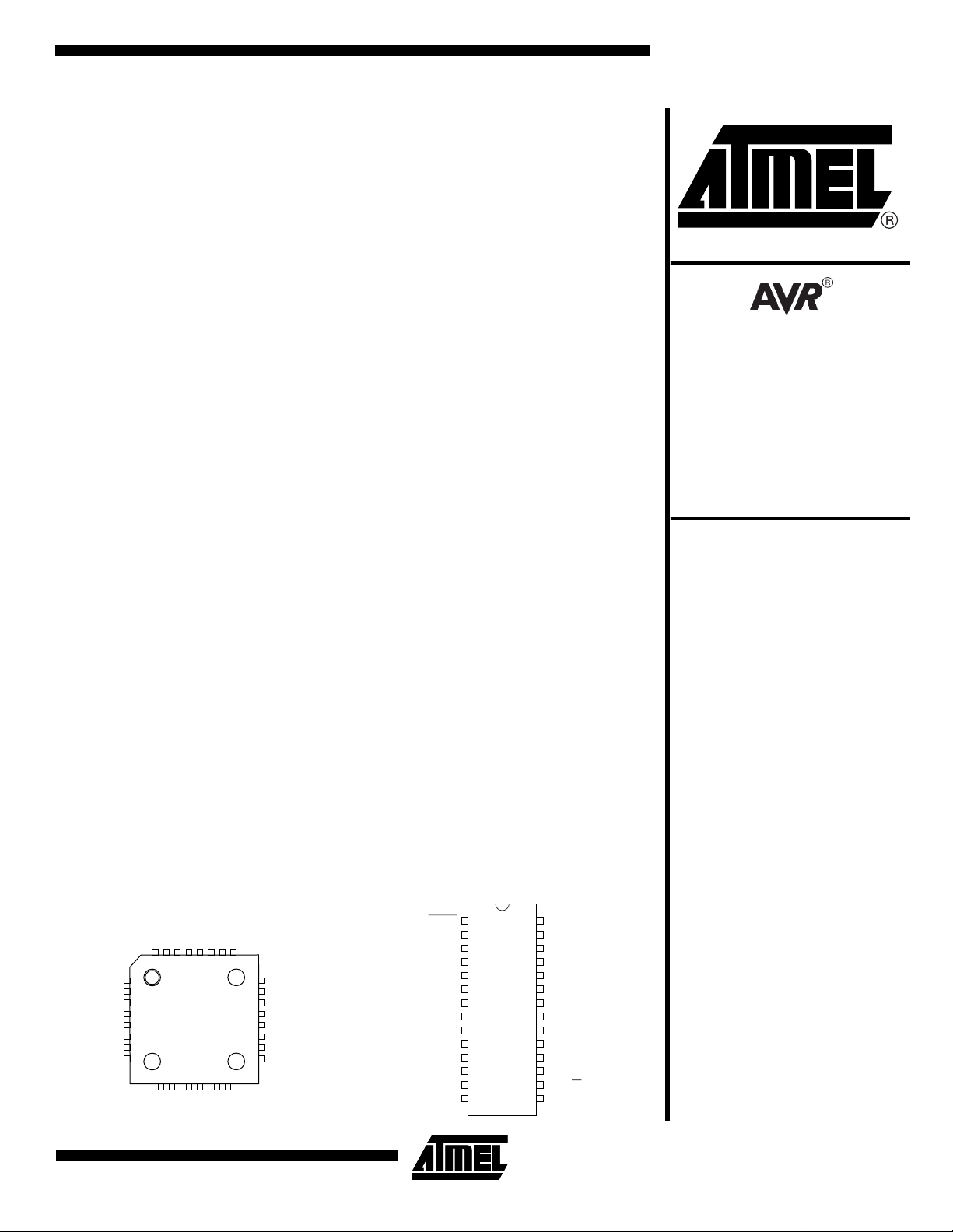
Pin Configurations
TQFP Top View PDIP
PD2 (INT0)
PD1 (TXD)
PD0 (RDX)
RESET
PC5 (ADC5)
PC4 (ADC4)
PC3 (ADC3)
PC2 (ADC2)
(INT1) PD3
(T0) PD4
VCC
GND
XTAL1
XTAL2
32313029282726
1
2
3
NC
4
5
6
NC
7
8
9101112131415
(T1) PD5
(AIN0) PD6
(AIN1) PD7
(SS) PB2
(ICP) PB0
(OC1) PB1
25
16
(MOS1) PB3
(MOS0) PB4
24
23
22
21
20
19
18
17
PC1 (ADC1)
PC0 (ADC0)
NC
AGND
AREF
NC
AVCC
PB5 (SCK)
RESET
(RXD) PD0
(TXD) PD1
(INT0) PD2
(INT1) PD3
(T0) PD4
VCC
GND
XTAL1
XTAL2
(T1) PD5
(AIN0) PD6
(AIN1) PD7
(ICP) PB0
1
2
3
4
5
6
7
8
9
10
11
12
13
14
28
27
26
25
24
23
22
21
20
19
18
17
16
15
PC5 (ADC5)
PC4 (ADC4)
PC3 (ADC3)
PC2 (ADC2)
PC1 (ADC1)
PC0 (ADC0)
AGND
AREF
AVCC
PB5 (SCK)
PB4 (MISO)
PB3 (MOSI)
PB2 (SS)
PB1 (OC1)
Rev. 1042DS–04/99
Note: This is a summary document. For the complete 103 page
document, please visit our Web site at www.atmel.com or e-mail
at literature@atmel.com and request literature #1042D.
1
Description
The AT90S2333/4433 is a low-power CMOS 8-bit microcontroller based on the AVR RISC architecture. By executing powerful instructions in a single clock cycle, the AT90S2333/4433 achieves throughputs approaching 1 MIPS per MHz allowing
the system designer to optimize power consumption versus processing speed.
The AVR core combines a rich instruction set with 32 general purpose working registers. All the 32 registers are directly
connected to the Arithmetic Logic Unit (ALU), allowing two independent registers to be accessed in one single instruction
executed in one clock cycle. The resulting architecture is more code efficient while achieving throughputs up to ten times
faster than conventional CISC microcontrollers.
The AT90S2333/4433 provides the following features: 2K/4K bytes of In-System Programmable Flash, 128/256 bytes
EEPROM, 128 bytes SRAM, 20 general purpose I/O lines, 32 general purpose working registers, two flexible
timer/counters with compare modes, internal and external interrupts, a programmable serial UART, 6-channel, 10-bit ADC,
programmable Watchdog Timer with internal oscillator, an SPI serial port and two software selectable power saving modes.
The Idle mode stops the CPU while allowing the SRAM, timer/counters, SPI port and interrupt system to continue functioning. The Power Down mode saves the register contents but freezes the oscillator, disabling all other chip functions until the
next interrupt or hardware reset.
The device is ma nufac tured using Atmel ’s h igh density nonv olatile memor y t echnolog y. The on- chip Fl ash p rogram memory can be reprogrammed in-system through an SPI serial interface or by a conventional nonvolatile memory programmer.
By combining a RISC 8-bit CPU with In-System Programmable Flash on a monolithic chip, the Atmel AT90S2333/4433 is a
powerful microcontroller that provides a highly flexible and cost effective solution to many embedded control applications.
The AT90S2333/4433 AVR is s uppo rt ed with a ful l s uit e of prog ra m and syste m de vel op men t tool s i nclud ing : C compilers,
macro assemblers, program debugger/simulators, in-circuit emulators, and evaluation kits.
Table 1. Comparison Table
Device Flash EEPROM SRAM Voltage Range Frequency
AT90S2333 2K 128B 128B 4.0V - 6.0V 0 - 8 MHz
AT90LS2333 2K 128B 128B 2.7V - 6.0V 0 - 4 MHz
AT90S4433 4K 256B 128B 4.0V - 6.0V 0 - 8 MHz
AT90LS4433 4K 256B 128B 2.7V - 6.0V 0 - 4 MHz
2
AT90S/LS2333 and AT90S/LS4433
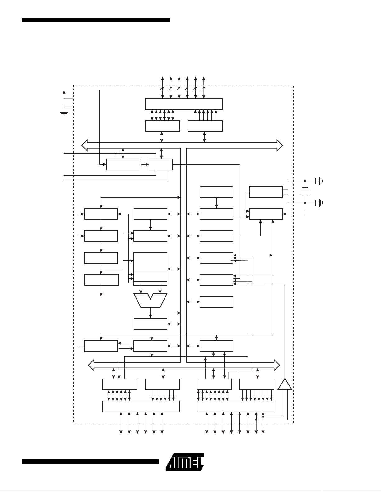
Block Diagram
Figure 1. The AT90S2333/4433 Block Diagram
VCC
AT90S/LS2333 and AT90S/LS4433
PC0 - PC5
PORTC DRIVERS
GND
AVCC
AGND
AREF
PROGRAM
COUNTER
PROGRAM
FLASH
INSTRUCTION
REGISTER
INSTRUCTION
DECODER
CONTROL
LINES
DATA REGISTER
PORTC
ANALOG MUX ADC
STACK
POINTER
SRAM
GENERAL
PURPOSE
REGISTERS
X
Y
Z
ALU
REG. PORTC
8-BIT DATA BUS
DATA DIR.
INTERNAL
OSCILLATOR
WATCHDOG
TIMER
MCU CONTROL
REGISTER
TIMER/
COUNTERS
INTERRUPT
UNIT
EEPROM
OSCILLATOR
TIMING AND
CONTROL
XTAL1
XTAL2
RESET
PROGRAMMING
LOGIC
DATA REGISTER
PORTB
PORTB DRIVERS
STATUS
REGISTER
PB0 - PB5
SPI
DATA DIR.
REG. PORTB
UART
DATA REGISTER
PORTD
PORTD DRIVERS
PD0 - PD7
DATA DIR.
REG. PORTD
+
COMPARATOR
ANALOG
3

Pin Descriptions
VCC
Supply voltage
GND
Ground
Port B (PB5..PB0)
Port B is a 6-bit bi-directional I/O port with internal pullup resistors. The Port B output buffers can sink 20 mA. As inputs,
Port B pins that are externally pulled low will source current if the pull-up resistors are activated.
Port B also serves the functions of various special features of the AT90S2333/4433.
The port B pins are tristated when a reset condition becomes active, even if the clock is not running.
Port C (PC5..PC0)
Port C is a 6-bit bi-directional I/O port with internal pullup resistors. The Port C output buffers can sink 20 mA. As inputs,
Port C pins that are ex ter na lly pul le d l ow wi ll s our ce c ur rent if the pull-up resistor s ar e a ctiv ated . P or t C a lso s er ves as the
analog inputs to the A/D Converter.
The port C pins are tristated when a reset condition becomes active, even if the clock is not running.
Port D (PD7..PD0)
Port D is an 8-bit bi-di r ectio nal I/O port with internal pull-up resi st or s. The P or t D ou tput buff er s can si nk 20 m A. A s inp uts ,
Port D pins that are externally pulled low will source current if the pull-up resistors are activated.
Port D also serves the functions of various special features of the AT90S2333/4433.
The port D pins are tristated when a reset condition becomes active, even if the clock is not running.
RESET
Reset input. An exter nal res et is gen erate d by a lo w le vel on the RESET pin. Res et p ul ses l on ger th an 5 0 n s w ill g ener a te
a reset, even if the clock is not running. Shorter pulses are not guaranteed to generate a reset.
XTAL1
Input to the inverting oscillator amplifier and input to the internal clock operating circuit.
XTAL2
Output from the inverting oscillator amplifier
AVCC
This is the supply volt age pin for the A/D Conv erter. It should be ext ernally conn ected to V
Datasheet for details on operation of the ADC.
AREF
This is the analog reference input for the A/D Converter. For ADC operations, a voltage in the range 2.7V to AVCC must be
applied to this pin.
AGND
If the board has a separate ana log ground plane, this pin should be con nec ted to thi s gro und pla ne. Ot he rwis e, c onn ec t to
GND.
via a low-pass filter. Se e
CC
4
AT90S/LS2333 and AT90S/LS4433

AT90S/LS2333 and AT90S/LS4433
Architectural Overview
The fast-access register file concept contains 32 x 8-bit general purpose working registers with a single clock cycle access
time. This means th at d ur ing one single clock cycle , on e A r ith meti c Log ic Uni t (A LU) op er ati on is ex ec ute d. Two ope ra nds
are output from the register file, the operation is executed, and the result is stored back in the register file - in one clock
cycle.
Six of the 32 registers can be used as three 16-bits indirect address register pointers for Data Space addressing - enabling
efficient address cal culation s. O ne of the three address point ers is also used a s the ad dress pointer for the c onst ant tabl e
look up function. These added function registers are the 16-bits X-register, Y-register and Z-register.
The ALU supports arithmetic and logic functions between registers or between a constant and a register. Single register
operations are also executed in the ALU. Figure 2 shows the AT90S2333/4433 AVR RISC microcontroller architecture.
In addition to the register operation, the conventional memory addressing modes can be used on the register file as well.
This is enabled by the fa ct th at the regis ter file is as signe d the 32 lowerm ost Data S pace a ddre sses ($00 - $1F) , al lowin g
them to be accessed as though they were ordinary memory locations.
Figure 2. The AT90S2333/4433 AVR RISC Architecture
AVR
1K/2K X 16
Program
Memory
Instruction
Register
Instruction
Decoder
Control Lines
AT90S2333/4433 Architecture
Data Bus 8-bit
Program
Counter
Direct Addressing
Indirect Addressing
Status
and Control
32 x 8
General
Purpose
Registrers
ALU
128 x 8
Data
SRAM
Interrupt
Unit
SPI
Unit
Serial
UART
8-bit
Timer/Counter
16-bit
Timer/Counter
with PWM
Watchdog
Timer
128/256 x 8
EEPROM
20
I/O Lines
Analog to Digital
Converter
Analog
Comparator
5

The I/O memory space contains 64 addresses for CPU peripheral functions a s Control Registers, Timer/Counters, A/Dconverters, and other I/O functions. The I/O Memory can be accessed directly, or as the Data Space locations following
those of the register file, $20 - $5F.
The AVR uses a Harvard architecture concept - with separate memories and buses for program and data. The program
memory is executed with a two stage pipeline. While one instruction is being executed, the next instruction is pre-fetched
from the program memory. This concept enables instructions to be executed in every clock cycle.
The program memory is In-System Programmable Flash memory.
With the relativ e jump an d call i nstru ctions , the whol e 1K/2K word a ddress space is di rect ly acces sed. Mo st AVR i nstru c-
tions have a single 16-bit word format. Every program memory address contains a 16- or 32-bit instruction.
During interrupts and su broutine ca lls, the retu rn addr ess program counte r (P C) is s tored on the stack. The st ack is effec-
tively alloca ted in the ge neral da ta SRAM, an d conseq uently th e stack size is onl y limite d by the total SRAM size and the
usage of the SRAM. All use r progr ams must in itial ize the SP in the re set routi ne (bef ore su broutine s or inter rupts ar e executed). The 8-bit stack pointer SP is read/write accessible in the I/O space.
The 128 bytes data SRAM can be easily accessed through the five different addressing modes supported in the AVR
architecture.
The memory spaces in the AVR
Figure 3. AT90S2333/4433 Memory Maps
architecture are all linear and regular memory maps.
Data MemoryProgram Memory
Program Flash
(1K/2K x 16)
$000
32 Gen. Purpose
Working Registers
64 I/O Registers
Internal SRAM
(128 x 8)
$0000
$001F
$0020
$005F
$0060
$00DF
$3FF/ $7FF
A flexible interrupt module has its control registers in the I/O space with an additional global interrupt enable bit in the status
register. All the different interrup ts have a sepa rate inter rupt vecto r in the interrupt ve ctor tab le at the beginn ing of the program memory. The different int errupts have pr iority in acco rdance with thei r interrupt vec tor position . The lower the
interrupt vector address, the higher the priority.
6
AT90S/LS2333 and AT90S/LS4433

AT90S/LS2333 and AT90S/LS4433
Register Summary
Address Name Bit 7 Bit 6 Bit 5 Bit 4 Bit 3 Bit 2 Bit 1 Bit 0
$3F ($5F) SREG I T H S V N Z C
$3E ($5E) Reserved
$3D ($5D) SP SP7 SP6 SP5 SP4 SP3 SP2 SP1 SP0
$3C ($5C) Reserved
$3B ($5B) GIMSK INT1 INT0 - - - - - $3A ($5A) GIFR INTF1 INTF0
$39 ($59) TIMSK TOIE1 OCIE1 - - TICIE1 -TOIE0 $38 ($58) TIFR TOV1 OCF1
$37 ($57) Reserved
$36 ($56) Reserved
$35 ($55) MCUCR - SE SM ISC11 ISC10 ISC01 ISC00
$34 ($54) MCUSR
$33 ($53) TCCR0
$32 ($52) TCNT0 Timer/Counter0 (8 Bits)
$31 ($51) Reserved
$30 ($50) Reserved
$2F ($4F) TCCR1A COM11 COM10 - - - -PWM11PWM10
$2E ($4E) TCCR1B ICNC1 ICES1
$2D ($4D) TCNT1H Timer/Counter1 - Counter Register High Byte
$2C ($4C) TCNT1L Timer/Counter1 - Counter Register Low Byte
$2B ($4B) OCR1H Timer/Counter1 - Output Compare Register High Byte
$2A ($4A) OCR1L Timer/Counter1 - Output Compare Register Low Byte
$29 ($49) Reserved
$28 ($48) Reserved
$27 ($47) ICR1H Timer/Counter1 - Input Capture Register High Byte
$26 ($46) ICR1L Timer/Counter1 - Input Capture Register Low Byte
$25 ($45) Reserved
$24 ($44) Reserved
$23 ($43) Reserved
$22 ($42) Reserved
$21 ($41) WDTCR - - - WDTOE WDE WDP2 WDP1 WDP0
$20 ($40) Reserved
$1F ($3F) Reserved
$1E ($3E) EEAR EEPROM Address Register
$1D ($3D) EEDR EEPROM Data Register
$1C ($3C) EECR
$1B ($3B) Reserved
$1A ($3A) Reserved
$19 ($39) Reserved
$18 ($38) PORTB - - PORTB5 PORTB4 PORTB3 PORTB2 PORTB1 PORTB0
$17 ($37) DDRB
$16 ($36) PINB
$15 ($35) PORTC
$14 ($34) DDRC
$13 ($33) PINC
$12 ($32) PORTD PORTD7 PORTD6 PORTD5 PORTD4 PORTD3 PORTD2 PORTD1 PORTD0
$11 ($31) DDRD DDD7 DDD6 DDD5 DDD4 DDD3 DDD2 DDD1 DDD0
$10 ($30) PIND PIND7 PIND6 PIND5 PIND4 PIND3 PIND2 PIND1 PIND0
$0F ($2F) SPDR SPI Data Register
$0E ($2E) SPSR SPIF WCOL
$0D ($2D) SPCR SPIE SPE DORD MSTR CPOL CPHA SPR1 SPR0
$0C ($2C) UDR UART I/O Data Register
$0B ($2B) UCSRA RXC TXC UDRE FE OR
$0A ($2A) UCSRB RXCIE TXCIE UDRIE RXEN TXEN CHR9 RXB8 TXB8
$09 ($29) UBRR UART Baud Rate Register
$08 ($28) ACSR ACD
$07 ($27) ADMUX
$06 ($26) ADCSR ADEN ADSC ADFR ADIF ADIE ADPS2 ADPS1 ADPS0
$05 ($25) ADCH
$04 ($24) ADCL ADC7 ADC6 ADC5 ADC4 ADC3 ADC2 ADC1 ADC0
$03 ($23) UBRRHI
- - - - - - - -
- - ICF1 -TOV0 -
- - - - WDRF BORF EXTRF PORF
- - - - - CS02 CS01 CS00
- - CTC1 CS12 CS11 CS10
- - - - EERIE EEMWE EEWE EERE
- - DDB5 DDB4 DDB3 DDB2 DDB1 DDB0
- - PINB5 PINB4 PINB3 PINB2 PINB1 PINB0
- - PORTC5 PORTC4 PORTC3 PORTC2 PORTC1 PORTC0
- - DDC5 DDC4 DDC3 DDC2 DDC1 DDC0
- - PINC5 PI NC4 PINC3 PINC2 PINC1 PINC0
- - - - - -
- - -
AINBG ACO ACI ACIE ACIC ACIS1 ACIS0
- ADCBG - - - MUX2 MUX1 MUX0
- - - - - - ADC9 ADC8
UART Baud Rate Register High
7

Register Summary (Continued)
Address Name Bit 7 Bit 6 Bit 5 Bit 4 Bit 3 Bit 2 Bit 1 Bit 0
$02 ($22) Reserved
$01 ($21) Reserved
$00 ($20) Reserved
Notes: 1. For compatibility with future devices, reserved bits should be written to zero if accessed. Reserved I/O memory addresses
should never be written.
2. Some of the status flags are cleared by writing a logical one to them. Note that the CBI and SBI instructions will operate on
all bits in the I/O register, writing a one back into any flag read as set, thus clearing the flag. The CBI and SBI instructions
work with registers $00 to $1F only.
8
AT90S/LS2333 and AT90S/LS4433

AT90S/LS2333 and AT90S/LS4433
Instruction Set Summary
Mnemonics Operands Description Operation Flags #Clocks
ARITHMETIC AND LOGIC INSTRUCTIONS
ADD Rd, Rr Add two Registers Rd ← Rd + Rr Z,C,N,V,H 1
ADC Rd, Rr Add with Carry two Registers Rd ← Rd + Rr + C Z,C,N,V,H 1
ADIW Rdl,K Add Immediate to Word Rdh:Rdl ← Rdh:Rdl + K Z,C,N,V,S 2
SUB Rd, Rr Subtract two Registers Rd ← Rd - Rr Z,C,N,V,H 1
SUBI Rd, K Subtract Constant from Register Rd ← Rd - K Z,C,N,V,H 1
SBC Rd, Rr Subtract with Carry two Registers Rd ← Rd - Rr - C Z,C,N,V,H 1
SBCI Rd, K Subtract with Carry Constant from Reg. Rd ← Rd - K - C Z,C,N,V,H 1
SBIW Rdl,K Subtract Immediate from Word Rdh:Rdl ← Rdh:Rdl - K Z,C,N,V,S 2
AND Rd, Rr Logical AND Registers Rd ← Rd • Rr Z,N,V 1
ANDI Rd, K Logical AND Register and Constant Rd ← Rd • K Z,N,V 1
OR Rd, Rr Logical OR Registers Rd ← Rd v Rr Z,N,V 1
ORI Rd, K Logical OR Register and Constant Rd ← Rd v K Z,N,V 1
EOR Rd, Rr Exclusive OR Registers Rd ← Rd ⊕ Rr Z,N,V 1
COM Rd One’s Complement Rd ← $FF − Rd Z,C,N,V 1
NEG Rd Two’s Complement Rd ← $00 − Rd Z,C,N,V,H 1
SBR Rd,K Set Bit(s) in Register Rd ← Rd v K Z,N,V 1
CBR Rd,K Clear Bit(s) in Register Rd ← Rd • ($FF - K) Z,N,V 1
INC Rd Increment Rd ← Rd + 1 Z,N,V 1
DEC Rd Decrement Rd ← Rd − 1 Z,N,V 1
TST Rd Test for Zero or Minus Rd ← Rd • Rd Z,N,V 1
CLR Rd Cle ar Register Rd ← Rd ⊕ Rd Z,N,V 1
SER Rd Set Register Rd ← $FF None 1
BRANCH INSTRUCTIONS
RJMP k Relative Jump PC ← PC + k + 1 None 2
IJMP Indirect Jump to (Z) PC ← Z None 2
RCALL k Relative Subroutine Call PC ← PC + k + 1 None 3
ICALL Indirect Call to (Z) PC ← ZNone3
RET Subroutine Return PC ← STACK No n e 4
RETI Interrupt Return PC ← STACK I 4
CPSE Rd,Rr Compare, Skip if Equal if (Rd = Rr) PC ← PC + 2 or 3 None 1 / 2 / 3
CP Rd,Rr Compare Rd − Rr Z, N,V,C,H 1
CPC Rd,Rr Compare with Carry Rd − Rr − C Z, N,V,C,H 1
CPI Rd,K Compare Register with Immediate Rd − K Z, N,V,C,H 1
SBRC Rr, b Skip if Bit in Register Cleared if (Rr(b)=0) PC ← PC + 2 or 3 None 1 / 2 / 3
SBRS Rr, b Skip if Bit in Register is Set if (Rr(b)=1) PC ← PC + 2 or 3 None 1 / 2 / 3
SBIC P, b Skip if Bit in I/O Register Cleared if (P(b)=0) PC ← PC + 2 or 3 None 1 / 2 / 3
SBIS P, b Skip if Bit in I/O Register is Set if (P(b)=1) PC ← PC + 2 or 3 None 1 / 2 / 3
BRBS s, k Branch if Status Flag Set if (SREG(s) = 1) then PC←PC+k + 1 None 1 / 2
BRBC s, k Branch if Status Flag Cleared if (SREG(s) = 0) then PC←PC+k + 1 None 1 / 2
BREQ k Branch if Equal if (Z = 1) then PC ← PC + k + 1 None 1 / 2
BRNE k Branch if Not Equal if (Z = 0) then PC ← PC + k + 1 None 1 / 2
BRCS k Branch if Carry Set if (C = 1) then PC ← PC + k + 1 None 1 / 2
BRCC k Branch if Carry Cleared if (C = 0) then PC ← PC + k + 1 None 1 / 2
BRSH k Branch if Same or Higher if (C = 0) then PC ← PC + k + 1 None 1 / 2
BRLO k Branch if Lower if (C = 1) then PC ← PC + k + 1 None 1 / 2
BRMI k Branch if Minus if (N = 1) then PC ← PC + k + 1 None 1 / 2
BRPL k Branch if Plus if (N = 0) then PC ← PC + k + 1 None 1 / 2
BRGE k Branch if Greater or Equal, Signed if (N ⊕ V= 0) then PC ← PC + k + 1 None 1 / 2
BRLT k Branch if Less Than Zero, Signed if (N ⊕ V= 1) then PC ← PC + k + 1 None 1 / 2
BRHS k Branch if Half Carry Flag Set if (H = 1) then PC ← PC + k + 1 None 1 / 2
BRHC k Branch if Half Carry Flag Cleared if (H = 0) then PC ← PC + k + 1 None 1 / 2
BRTS k Branch if T Flag Set if (T = 1) then PC ← PC + k + 1 None 1 / 2
BRTC k Branch if T Flag Cleared if (T = 0) then PC ← PC + k + 1 None 1 / 2
BRVS k Branch if Overflow Flag is Set if (V = 1) then PC ← PC + k + 1 None 1 / 2
BRVC k Branch if Overflow Flag is Cleared if (V = 0) then PC ← PC + k + 1 None 1 / 2
BRIE k Branch if Interrupt Enabled if ( I = 1) then PC ← PC + k + 1 None 1 / 2
BRID k Branch if Interrupt Disabled if ( I = 0) then PC ← PC + k + 1 None 1 / 2
9

Instruction Set Summary (Continued)
Mnemonics Operands Description Operation Flags #Clocks
DATA TRANSFER INSTRUCTIONS
MOV Rd, Rr Move Between Registers Rd ← Rr None 1
LDI Rd, K Load Immediate Rd ← KNone1
LD Rd, X Load Indirect Rd ← (X) None 2
LD Rd, X+ Load Indirect and Post-Inc. Rd ← (X), X ← X + 1 None 2
LD Rd, - X Load Indirect and Pre-Dec. X ← X - 1, Rd ← (X) None 2
LD Rd, Y Load Indirect Rd ← (Y) None 2
LD Rd, Y+ Load Indirect and Post-Inc. Rd ← (Y), Y ← Y + 1 None 2
LD Rd, - Y Load Indirect and Pre-Dec. Y ← Y - 1, Rd ← (Y) None 2
LDD Rd,Y+q Load Indirect with Displacement Rd ← (Y + q) None 2
LD Rd, Z Load Indirect Rd ← (Z) None 2
LD Rd, Z+ Load Indirect and Post-Inc. Rd ← (Z), Z ← Z+1 None 2
LD Rd, -Z Load Indirect and Pre-Dec. Z ← Z - 1, Rd ← (Z) None 2
LDD Rd, Z+q Load Indirect with Displacement Rd ← (Z + q) None 2
LDS Rd, k Load Direct from SRAM Rd ← (k) None 2
ST X, Rr Store Indirect (X) ← Rr None 2
ST X+, Rr Store Indirect and Post-Inc. (X) ← Rr, X ← X + 1 None 2
ST - X, Rr Store Indirect and Pre-Dec. X ← X - 1, (X) ← Rr None 2
ST Y, Rr Store Indirect (Y) ← Rr None 2
ST Y+, Rr Store Indirect and Post-Inc. (Y) ← Rr, Y ← Y + 1 None 2
ST - Y, Rr Store Indirect and Pre-Dec. Y ← Y - 1, (Y) ← Rr None 2
STD Y+q,Rr Store Indirect with Displacement (Y + q) ← Rr None 2
ST Z, Rr Store Indirect (Z) ← Rr None 2
ST Z+, Rr Store Indirect and Post-Inc. (Z) ← Rr, Z ← Z + 1 None 2
ST -Z, Rr Store Indirect and Pre-Dec. Z ← Z - 1, (Z) ← Rr None 2
STD Z+q,Rr Store Indirect with Displacement (Z + q) ← Rr None 2
STS k, Rr Store Direct to SRAM (k) ← Rr None 2
LPM Load Program Memory R0 ← (Z) None 3
IN Rd, P In Port Rd ← PNone1
OUT P, Rr Out Port P ← Rr None 1
PUSH Rr Push Register on Stack STACK ← Rr None 2
POP Rd Pop Register from Stack Rd ← STACK Non e 2
BIT AND BIT-TEST INSTRUCTIONS
SBI P,b Set Bit in I/O Register I/O(P,b) ← 1None2
CBI P,b Clear Bit in I/O Register I/O(P,b) ← 0None2
LSL Rd Logical Shift Left Rd(n+1) ← Rd(n), Rd(0) ← 0 Z,C,N,V 1
LSR Rd Logical Shift Right Rd(n) ← Rd(n+1), Rd(7) ← 0 Z,C,N,V 1
ROL Rd Rotate Left Through Carry Rd(0)←C,Rd(n+1)← Rd(n),C←Rd(7) Z,C,N,V 1
ROR Rd Rotate Right Through Carry Rd(7)←C,Rd(n)← Rd(n+1),C←Rd(0) Z,C,N,V 1
ASR Rd Arithmetic Shift Right Rd(n) ← Rd(n+1), n=0..6 Z,C,N,V 1
SWAP Rd Swap Nibbles Rd(3..0)←Rd(7..4),Rd(7..4)←Rd(3..0) None 1
BSET s Flag Set SREG(s) ← 1 SREG(s) 1
BCLR s Flag Clear SREG(s) ← 0 SREG(s) 1
BST Rr, b Bit Store from Register to T T ← Rr(b) T 1
BLD Rd, b Bit load from T to Register Rd(b) ← TNone1
SEC Set Carry C ← 1C1
CLC Clear Carry C ← 0 C 1
SEN Set Negative Flag N ← 1N1
CLN Clear Negative Flag N ← 0 N 1
SEZ Set Zero Flag Z ← 1Z1
CLZ Clear Zero Flag Z ← 0 Z 1
SEI Global Interrupt Enable I ← 1I1
CLI Global Interrupt Disable I ← 0 I 1
SES Set Signed Test Flag S ← 1S1
CLS Clear Signed Test Flag S ← 0 S 1
SEV Set Twos Complement Overflow. V ← 1V1
CLV Clear Twos Complement Overflow V ← 0 V 1
SET Set T in SREG T ← 1T1
CLT Clear T in SREG T ← 0 T 1
SEH Set Half Carry Flag in SREG H ← 1H1
CLH Clear Half Carry Flag in SREG H ← 0 H 1
NOP No Operation None 1
SLEEP Sleep (see specific descr. for Sleep function) None 3
WDR Watchdog Reset (see specific descr. for WDR/timer) None 1
10
AT90S/LS2333 and AT90S/LS4433

AT90S/LS2333 and AT90S/LS4433
Ordering Information
Power Supply Speed (MHz) Ordering Code Package Operation Range
2.7 - 6.0V 4 AT90LS2333-4AC
AT90LS2333-4PC
AT90LS2333-4AI
AT90LS2333-4PI
4.0 - 6.0V 8 AT90S2333-8AC
AT90S2333-8PC
AT90S2333-8AI
AT90S2333-8PI
2.7 - 6.0V 4 AT90LS4433-4AC
AT90LS4433-4PC
AT90LS4433-4AI
AT90LS4433-4PI
4.0 - 6.0V 8 AT90S4433-8AC
AT90S4433-8PC
AT90S4433-8AI
AT90S4433-8PI
32A
28P3
32A
28P3
32A
28P3
32A
28P3
32A
28P3
32A
28P3
32A
28P3
32A
28P3
Commercial
(0
°C to 70°C)
Industrial
(-40
°C to 85°C)
Commercial
(0
°C to 70°C)
Industrial
(-40
°C to 85°C)
Commercial
(0
°C to 70°C)
Industrial
(-40
°C to 85°C)
Commercial
(0
°C to 70°C)
Industrial
(-40
°C to 85°C)
Package Type
28P3 28-lead, 0.300” Wide, Plastic Dual in Line Package (PDIP)
32A 32-lead, Thin (1.0 mm) Plastic Gull Wing Quad Flat Package (TQFP)
11

Pac kaging Information
28P3, 28-lead, 0.300” Wide,
Plastic Dual Inline Package (PDIP)
Dimensions in Inches and (Millimeters)
32A, 32-lead, Thin (1.0 mm) Plastic Gull Wing Quad
Flat Package (TQFP)
Dimensions in Millimeters and (Inches)
PIN 1 ID
0.80 (0.031) BSC
0.20 (0.008)
0.10 (0.004)
0.45 (0.018)
0.30 (0.012)
0˚
7˚
9.00 (0.354) BSC
7.00 (0.276) BSC
0.75 (0.030)
0.45 (0.018)
9.00 (0.354) BSC
1.20 (0.047) MAX
0.15 (0.006)
0.05 (0.002)
12
AT90S/LS2333 and AT90S/LS4433

Atmel Headquarters Atmel Operations
Corporate Headquarters
2325 Orchard Parkway
San Jose, CA 95131
TEL (408) 441- 0311
FAX (408) 487-2600
Europe
Atmel U.K., Ltd.
Coliseum Business Centre
Riverside Way
Camberley, Surrey GU15 3YL
England
TEL (44) 1276-686-677
FAX (44) 1276-686-697
Asia
Atmel Asia, Ltd.
Room 1219
Chinachem Golden Plaza
77 Mody Road Tsimhatsui
East Kowloon
Hong Kong
TEL (852) 2721 -9778
FAX (852) 2722-1369
Japan
Atmel Japan K.K.
9F, Tonetsu Shinkawa Bldg.
1-24-8 Shink awa
Chuo-ku, Tokyo 104-0033
Japan
TEL (81) 3-3523-3551
FAX (81) 3-3523-7581
Atmel Colorado Springs
1150 E. Cheyenne Mtn. Blvd.
Colorado Springs, CO 80906
TEL (719) 576-3300
FAX (719) 540-1759
Atmel Rousset
Zone Indu strie lle
13106 Rousset Cedex
France
TEL (33) 4-4253-6000
FAX (33) 4-4253-6001
Fax-on-Demand
North America:
1-(800) 292-8635
International:
1-(408) 441-0732
e-mail
literature@atmel.com
Web Site
http://www.atmel.com
BBS
1-(408) 436-4309
© Atmel Corporation 1999.
Atmel Corporation makes no warranty for the use of its products, other than those expressly contained in the Company’s standard warranty which is detailed in Atmel’s Terms and Conditions located on the Company’s web site. The Company assumes no responsibility for
any errors which may appear in this document, reserves the right to change devices or specifications detailed herein at any time without
notice, and does not make any commitment to update the information contained herein. No licenses to patents or other intellectual property of Atmel are granted by the Company in connection with the sale of Atmel products, expressly or by implication. Atmel’s products are
not authorized for use as critical components in life support devices or systems.
Marks bearing ® and/or ™ are registered trademarks and trademarks of Atmel Corporation.
Ter ms and product names in this document may be trademarks of others.
Printed on recycled paper.
1042DS–04/99/xM
 Loading...