

Datasheet AT90LS2343-4SI, AT90LS2343-4SC, AT90LS2343-4PI, AT90LS2343-4PC, AT90S2343-10SI Datasheet (ATMEL)
...
Features
•
Utilizes the
•
AVR
- High Performance and Low Power RISC Architecture
•
118 Powerful Instructions - Most Single Clock Cycle Execution
•
2K bytes of In-System Programmable ISP Flash
– SPI Serial Interface for In-System Programming
– Endurance: 1,000 Write/Eras e Cycles
•
128 bytes EEPROM
– Endurance: 100,000 Write/Erase Cycles
•
128 bytes Internal RAM
•
32 x 8 General Purpose Working Registers
– 3 AT90S/LS2323 Programmable I/O Lines
– 5 AT90S/LS2343 Programmable I/O Lines
•
VCC: 4.0 - 6.0V AT90S2323/AT90S2343
•
VCC: 2.7 - 6.0V AT90LS2323/AT90LS2343
•
Power-On Reset Circuit
•
Speed Grades: 0 - 10 MHz AT90S2323/AT90S2343
•
Speed Grades: 0 - 4 MHz AT90LS2323/AT90LS2343
•
Up to 10 MIPS Throughput at 10 MHz
•
One 8-Bit Timer/Counter with Separate Prescaler
•
External and Internal Interrupt Sources
•
Programmable Watchdog Timer with On-Chip Oscillator
•
Low Power Idle and Power Down Modes
•
Programming Lock for Flash Program and EEPROM Data Security
•
Selectable On-Chip RC Oscillator
•
8-Pin Device
®
AVR
Enhanced RISC Architecture
8-Bit
Microcontroller
with 2K Bytes of
In-System
Programmable
Flash
AT90S2323
Description
The AT90S/LS2323 and AT90S/LS2343 is a low-power CMOS 8-bit microcontrollers
based on the
in a single cloc k cycl e, the AT 90S/LS 2323 and A T90S/ LS2343 achieves throug hputs
approaching 1 MIPS per MHz allo wing the system desi gner to optimize powe r consumption versus processing speed.
The AVR core combines a rich instr uction set with 32 gene ral purpose working registers. All the 32 registers are directly connected to the Arithmetic Logic Unit (ALU),
allowing two indep endent r egisters to be acce ssed in one singl e instr uction execute d
in one clock cycle. Th e resulting arc hitecture is mor e code efficie nt while achievin g
throughputs up to ten times faster than conventional CISC microcontrollers.
®
AVR
enhanced RISC arch itectu re. By exec uting pow erful in struc tions
Pin Configuration
PDIP/SOIC
RESET
(CLOCK) PB3
PB4
GND
1
2
3
4
AT90S/LS2343 AT90S/LS2323
8
VCC
7
PB2 (SCK/T0)
6
PB1 (MISO/INT0)
5
PB0 (MOSI)
RESET
XTAL1
XTAL2
GND
1
2
3
4
8
VCC
7
PB2 (SCK/T0)
6
PB1 (MISO/INT0)
5
PB0 (MOSI)
AT90LS2323
AT90S2343
AT90LS2343
Preliminary
A T90S/LS2323
Rev. 1004AS–05/98
Note: This is a summary document. For the complete 34 page
document, please visit our website at
literature@atmel.com
and request literature #1004A.
www.atmel.com
or e-mail at
1
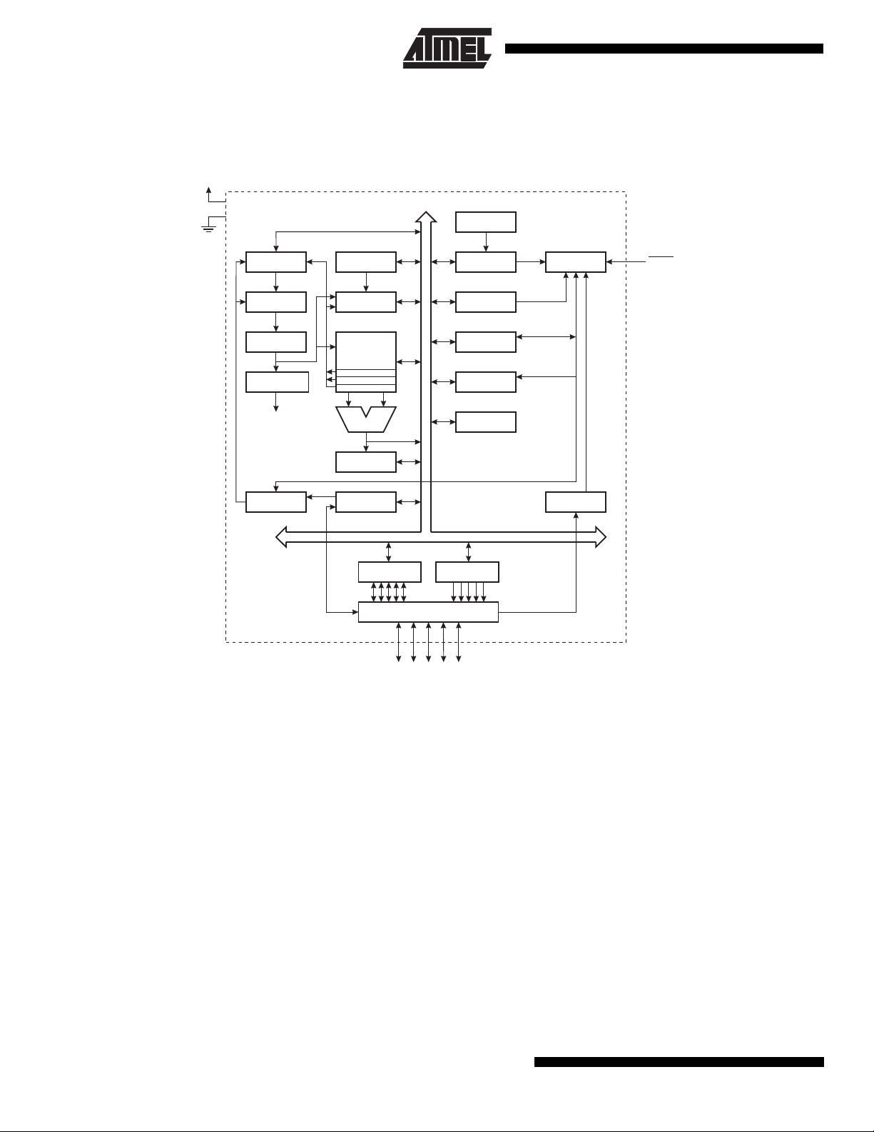
Block Diagram
Figure 1. The AT90S/LS2343 Block Diagram
VCC
GND
PROGRAM
COUNTER
STACK
POINTER
8-BIT DATA BUS
INTERNAL
OSCILLATOR
WATCHDOG
TIMER
TIMING AND
CONTROL
RESET
PROGRAM
FLASH
INSTRUCTION
REGISTER
INSTRUCTION
DECODER
CONTROL
LINES
PROGRAMMING
LOGIC
SRAM
GENERAL
PURPOSE
REGISTERS
X
Y
Z
ALU
STATUS
REGISTER
SPI
DATA REGISTER
PORTB
PORTB DRIVERS
PB0 - PB4
MCU CONTROL
REGISTER
TIMER/
COUNTER
INTERRUPT
UNIT
EEPROM
DATA DIR.
REG. PORTB
OSCILLATOR
2
AT90S/LS2323 and AT90S/LS2343
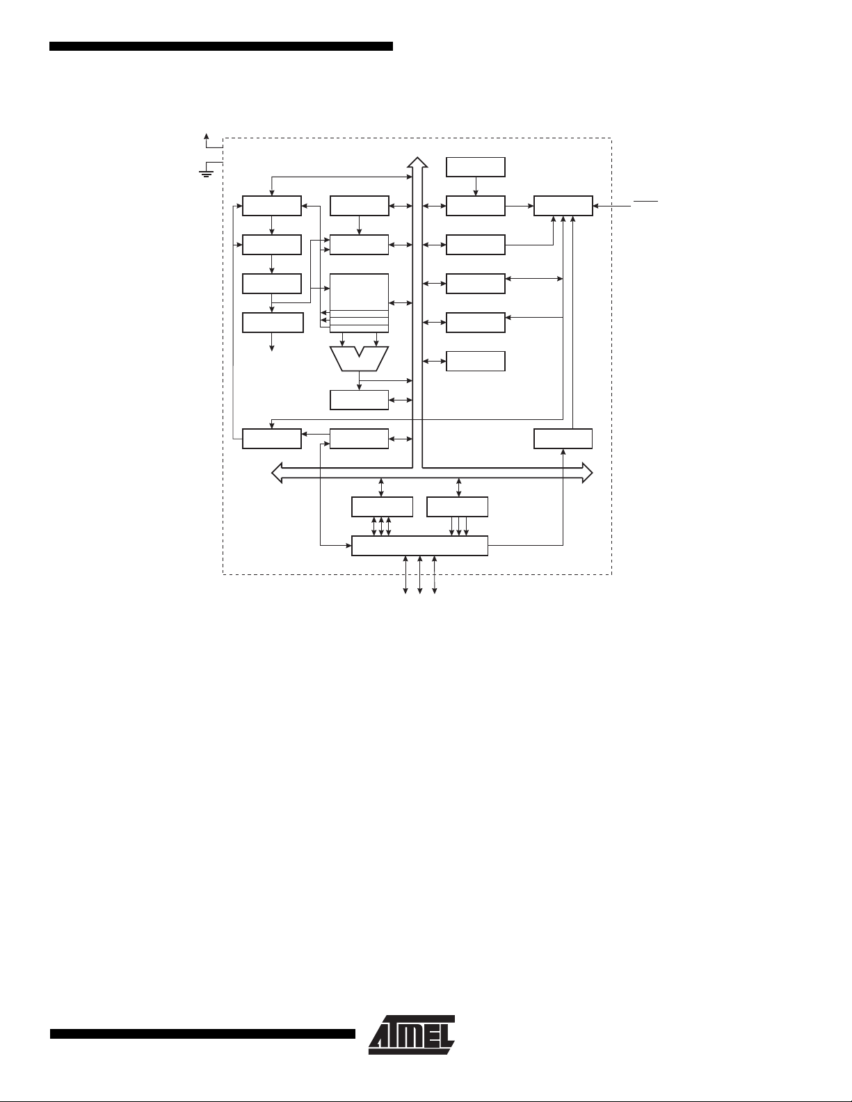
Figure 2. The AT90S/LS2323 Block Diagram
VCC
GND
PROGRAM
COUNTER
STACK
POINTER
AT90S/LS2323 and AT90S/LS2343
8-BIT DATA BUS
INTERNAL
OSCILLATOR
WATCHDOG
TIMER
TIMING AND
CONTROL
RESET
PROGRAM
FLASH
INSTRUCTION
REGISTER
INSTRUCTION
DECODER
CONTROL
LINES
PROGRAMMING
LOGIC
SRAM
GENERAL
PURPOSE
REGISTERS
X
Y
Z
ALU
STATUS
REGISTER
SPI
DATA REGISTER
PORTB
PORTB DRIVERS
Description
The AT90S/LS2323 and AT90S/LS2343 provides the following features: 2K bytes of In-System Programmable
Flash, 128 bytes EEPROM, 128 bytes SRAM, 3
(AT90S/LS2323) / 5 (AT90S/LS2343) general purpose I/O
lines, 32 general purpose workin g registers, an 8-bit
timer/counter, internal a nd externa l interru pts, progr ammable Watchdog Timer with internal oscillator, an SPI serial
port for Fla sh Memory down loading and two software
selectable power savi ng modes. The Idle Mo de stops the
CPU while allowing the SRAM, timer/counters, SPI port
and interrupt system to conti nue functioning. The pow er
down mode saves the register contents but freezes the
oscillator, disabling all other chip func tions until the next
interrupt or hardware reset.
The device is manufac tured using Atmel’s high density
non-volatile memory technology. The on-chip Flash allows
the program memory to be reprogrammed in-system
through an SPI serial interface. By combining an 8-bit RISC
CPU with ISP Flash on a monolithic chip, the Atmel
AT90S/LS2323 an d AT90S/LS234 3 is a powerful mi cro-
MCU CONTROL
REGISTER
TIMER/
COUNTER
INTERRUPT
UNIT
EEPROM
OSCILLATOR
DATA DIR.
REG. PORTB
PB0 - PB2
controller that provides a highly flexibl e and cost effective
solution to many embedded control applications.
The AT90S/LS2323 and AT90S/LS2343 AVR is supported
with a full suite of program and system development tools
including: C compilers, macro assemblers, program debugger/simulators, in-circuit emulators, and evaluation kits.
Comparison Between AT90S/LS2323
and AT90S/LS2343
The AT90S/LS2323 is intended for use with external quartz
crystal or ceramic resonator as the clock source. The startup time is fuse selectable as either 1 ms (suitable for
ceramic resonator) or 16 ms (suitable for crystal). The
device has three I/0 pins.
The AT90S/LS2343 is intended for use with either an external clock source or the internal RC oscillator as clock
source. The device has five I/0 pins.
3
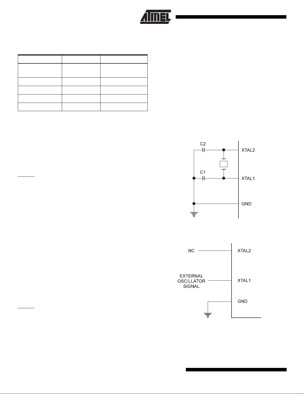
Table 1 summarizes the differences in features of the two
devices.
Table 1. Feature Difference Summary
Part AT90S/LS2323 AT90S/LS2343
On-chip oscillator
amplifier
Internal RC Clock no yes
PB3 usable never internal clock mode
PB4 usable never always
Startup time 1 ms / 16 ms 16 µs fixed
yes no
Pin Descriptions AT90S/LS2323
VCC
Supply voltage pin.
GND
Ground pin.
Port B (PB2..PB0)
Port B is a 3-bit bi-directional I/O port. Port pins can provide
internal pull-up resistors (selected for each bit).
RESET
Reset input. A low on thi s pin for t wo m achine c ycles while
the oscillator is running resets the device.
XTAL1
Input to the inverting os cillator ampl ifier and input to the
internal clock operating circuit.
XTAL2
Output from the inverting oscillator amplifier.
Pin Descriptions AT90S/LS2343
VCC
Supply voltage pin.
GND
Ground pin.
Port B (PB4..PB0)
Port B is a 5-bit bi-directional I/O port. Port pins can provide
internal pull-up resistors (selected for each bit). W hen the
device is clocked from an external clock source, PB3 is
used as the clock input.
RESET
Reset input. A low on thi s pin for t wo m achine c ycles while
the oscillator is running resets the device.
CLOCK
Clock signal input in external clock mode.
Clock Sources
The AT90S/LS2323 contains an inverting amplifier which
can be configured for us e as an on-chip oscillato r, as
shown in Figure 3. XTAL1 and XTAL2 ar e input and ou tput
respectively. Either a quartz crystal or a ceramic resonator
may be used. It is recommended to use the AT90S/LS2343
if an external clock source is used, since this gives an extra
I/O pin.
The AT90S/LS2343 can be clocked by an external clo ck
signal, as shown in Figure 4, or by the on-chip RC oscillator. This RC oscillator runs at a nominal frequency of 1
MHz (VCC = 5V). A fuse bit - RCEN - in the Flash mem ory
selects the on-chip RC oscillator as the clock source when
programmed ('0'). The AT90S/LS2343 is shipped with this
bit programmed.
Figure 3. Oscillator Connection
Figure 4. External Clock Drive Configuration
4
AT90S/LS2323 and AT90S/LS2343

AT90S/LS2323 and AT90S/LS2343
AT90S/LS2323 and AT90S/LS2343
Architectural Overview
The fast-access register file concept contains 32 x 8-bit
general purpose worki ng regis ters with a sing le clo ck cycle
access time. This means that during one single clock cycle,
one ALU (Arithmetic Logic Unit) operation is executed. Two
operands are output from the register file, the operation is
executed, and the res ult is stored b ack in th e regi ster fi le in one clock cycle.
Six of the 32 registers can be used as three 16-bits indirect
address register pointers for Data Space addres singenabling efficient address ca lculations. One of the three
address pointers is also used as the address pointer for the
constant table look up function. These added function registers are the 16-bit X-register, Y-register and Z-register.
The ALU supports arithmetic and logic functions be tween
registers or be tween a c onstant a nd a regi ster. S ingle re gister operations are also executed in the ALU. Figure 5
shows the AT90S/LS2 323 and AT90S/LS2343
Enhanced RISC microcontroller architecture.
In addition to the register operation, the conventional memory addressing modes can be used on the register file as
well. This is e nabled by t he fact that the registe r file is
assigned the 32 lo wermost Data Space addre sses ($00 $1F), allowing them to be accessed as though they were
ordinary memory locations.
The I/O memory space contains 64 addresses for CPU
peripheral fu nction s as Cont rol Reg isters, Timer /Coun ters,
AVR
A/D-converte rs, and o ther I/O fun ctions. The I/O me mory
can be accessed di rectly, or as the Data Spac e locations
following those of the register file, $20 - $5F.
AVR
The
ries and buses for program and data. The program memory
is accessed with a two stage pipeline. While one instruction
is being executed, the next instruction is pre-fetched from
the program memory. This concept enables instructions to
be executed in every clock cycle. The program memory is
in-system downloadable Flash memory.
With the relative jump and call instructions, the whole 1K
address space is dir ectly ac cessed. M ost
have a single 16-bit word for mat. Every progr am memory
address contains a 16- or 32-bit instruction.
During interrupts a nd subrou tine cal ls, the r eturn addr ess
program counter (PC) is stored on the stack. The stack is
effectively allocat ed in the gene ral data S RAM , and co nsequently the stack size is only limited by the total SRAM size
and the usage of the S RAM . Al l user programs must init ial ize the SP i n th e r eset ro utine (be fore su brouti nes or int errupts are executed). The 8-bit stack pointer SP is read/write
accessible in the I/O space.
The 128 bytes data SRAM + register file and I/O registers
can be easily accessed through the five different addressing modes supported in the
The memory spaces in the
and regular memory maps.
has Harvard architecture - with separate memo-
AVR
instructions
AVR
architecture.
AVR
architecture are all linear
5

Figure 5. The AT90S/LS2323 and AT90S/LS2343 AVR Enhanced RISC Architecture
AVR
AT90S2323/AT90S2343 Architecture
Data Bus 8-bit
Figure 6. Memory Maps
1K x 16
Program
Flash
Instruction
Register
Instruction
Decoder
Control Lines
Program
Counter
Direct Addressing
Status
and Test
32 x 8
General
Purpose
Registers
ALU
Indirect Addressing
128 x 8
Data
SRAM
Control
Registers
Interrupt
Unit
SPI
Unit
8-bit
Timer/Counter
Watchdog
Timer
I/O Lines
128 x 8
EEPROM
EEPROM
(128 x 8)
$000
$07F
6
AT90S/LS2323 and AT90S/LS2343

AT90S/LS2323 and AT90S/LS2343 Register Summary
Address Name Bit 7 Bit 6 Bit 5 Bit 4 Bit 3 Bit 2 Bit 1 Bit 0 Page
$3F ($5F) SREG I T H S V N Z C page 13
$3E ($5E) Reserved
$3D ($5D) SPL SP7 SP6 SP5 SP4 SP3 SP2 SP1 SP0 page 13
$3C ($5C) Reserved
$3B ($5B) GIMSK -INT0- - - - - - page 17
$3A ($5A) GIFR
$39 ($59) TIMSK
$38 ($58) TIFR
$37 ($57) Reserved
$36 ($56) Reserved
$35 ($55) MCUCR - -SESM- - ISC01 ISC00 page 16
$34 ($54) MCUSR
$33 ($53) TCCR0
$32 ($52) TCNT0 Timer/Counter0 (8 Bit) page 20
$31 ($51) Reserved
$30 ($50) Reserved
$2F ($4F) Reserved
$2E ($4E) Reserved
$2D ($4D) Reserved
$2C ($4C) Reserved
$2B ($4B) Reserved
$2A ($4A) Reserved
$29 ($49) Reserved
$28 ($48) Reserved
$27 ($47) Reserved
$26 ($46) Reserved
$25 ($45) Reserved
$24 ($44) Reserved
$23 ($43) Reserved
$22 ($42) Reserved
$21 ($41) WDTCR - - - WDTO WDE WDP2 WDP1 WDP0 page 21
$20 ($40) Reserved
$1F ($3F) Reserved
$1E ($3E) EEAR - EEPROM Address Register page 22
$1D ($3D) EEDR EEPROM Data register page 22
$1C ($3C) EECR
$1B ($3B) Reserved
$1A ($3A) Reserved
$19 ($39) Reserved
$18 ($38) PORTB - - - PORTB PORTB PORTB PORTB PORTB page 23
$17 ($37) DDRB
$16 ($36) PINB
$15 ($35) Reserved
$14 ($34) Reserved
$13 ($33) Reserved
$12 ($32) Reserved
$11 ($31) Reserved
$10 ($30) Reserved
$0F ($2F) Reserved
$0E ($2E) Reserved
$0D ($2D) Reserved
$0C ($2C) Reserved
$0B ($2B) Reserved
$0A ($2A) Reserved
$09 ($29) Reserved
$08 ($28) Reserved
… Reserved
$00 ($20) Reserved
-INTF0 page 17
- - - - - -TOIE0- page 15
- - - - - -TOV0- page 16
- - - - - - EXTRF PORF page 14
- - - - - CS02 CS01 CS00 page 20
- - - - - EEMW EEWE EERE page 22
- - - DDB4 DDB3 DDB2 DDB1 DDB0 page 23
- - - PINB4 PINB3 PINB2 PINB1 PINB0 page 23
7
AT90S/LS2323 and AT90S/LS2343

AT90S/LS2323 and AT90S/LS2343
AT90S/LS2323 and AT90S/LS2343 Instruction Set Summary
Mnemonics Operands Description Operation Flags #Clock
ARITHMETIC AND LOGIC INSTRUCTIONS
ADD Rd, Rr Add two Registers Rd
ADC Rd, Rr Add with Carry two Registers Rd
ADIW Rdl,K Add Immediate to Word Rdh:Rdl
SUB Rd, Rr Subtract two Registers Rd
SUBI Rd, K Subtract Constant from Register Rd
SBIW Rdl,K Subtract Immediate from Word Rdh:Rdl
SBC Rd, Rr Subtract with Carry two Registers Rd
SBCI Rd, K Subtract with Carry Constant from Reg. Rd
AND Rd, Rr Logical AND Registers Rd
ANDI Rd, K Logical AND Register and Constant Rd
OR Rd, Rr Logical OR Registers Rd
ORI Rd, K Logical OR Register and Constant Rd
EOR Rd, Rr Exclus ive OR Registers Rd
COM Rd One’s Complement Rd
NEG Rd Two’s Complement Rd
SBR Rd,K Set Bit(s) in Register Rd
CBR Rd,K Clear Bit(s) in Register Rd
INC Rd Increment Rd
DEC Rd Decrement Rd
TST Rd Test for Zero or Minus Rd
CLR Rd Clear Register Rd
SER Rd Set Register Rd
BRANCH INSTRUCTIONS
RJMP k Relative Jump PC
IJMP Indirect Jump to (Z) PC
RCALL k Relative Subroutine Call PC
ICALL Indirect Call to (Z) PC
RET Subroutine Return PC
RETI Interrupt Return PC
CPSE Rd,Rr Compare, Skip if Equal if (Rd = Rr) PC
CP Rd,Rr Com pare Rd
CPC Rd,Rr Compare with Carry Rd
CPI Rd,K Compare Register with Immediate Rd
SBRC Rr, b Skip if Bit in Register Cleared if (Rr(b)=0) PC
SBRS Rr, b Skip if Bit in Register is Set if (Rr(b)=1) PC
SBIC P, b Skip if Bit in I/O Register Cleared if (P(b) =0) PC
SBIS P, b Skip if Bit in I/O Register is Set if (R(b)=1) PC
BRBS s, k Branch if Status Flag Set if (SREG(s) = 1) then PC
BRBC s, k Branch if Status Flag Cleared if (SREG(s) = 0) then PC
BREQ k Branch if Equal if (Z = 1) then PC
BRNE k Branch if Not Equal if (Z = 0) then PC
BRCS k Branch if Carry Set if (C = 1) then PC
BRCC k Branch if Carry Cleared if (C = 0) then PC
BRSH k Branch if Same or Higher if (C = 0) then PC
BRLO k Branch if Lower if (C = 1) then PC
BRMI k Branch if Minus if (N = 1) then PC
BRPL k Branch if Plus if (N = 0) then PC
BRGE k Branch if Greater or Equal, Signed if (N
BRLT k Branch if Less Than Zero, Signed if (N
BRHS k Branch if Half Carry Flag Set if (H = 1) then PC
BRHC k Branch if Half Carry Flag Cleared if (H = 0) then PC
BRTS k Branch if T Flag Set if (T = 1) then PC
BRTC k Branch if T Flag Cleared if (T = 0) then PC
BRVS k Branch if Overflow Flag is Set if (V = 1) then PC
BRVC k Branch if Overflow Flag is Cleared if (V = 0) then PC
BRIE k Branch if Interrupt Enabled if ( I = 1) then PC
BRID k Branch if Interrupt Disabled if ( I = 0) then PC
← Rd + Rr Z,C,N,V,H 1
← Rd + Rr + C Z,C,N,V,H 1
← Rdh:Rdl + K Z,C,N,V,S 2
← Rd − Rr Z,C,N,V,H 1
← Rd − K Z,C,N,V,H 1
← Rdh:Rdl − K Z,C,N,V,S 2
← Rd − Rr − C Z,C,N,V,H 1
← Rd − K − C Z,C,N,V,H 1
← Rd • Rr Z,N,V 1
← Rd • K Z,N,V 1
← Rd v Rr Z,N,V 1
← Rd v K Z,N,V 1
← Rd ⊕ Rr Z,N,V 1
← $FF − Rd Z,C,N,V 1
← $00 − Rd Z,C,N,V,H 1
← Rd v K Z,N,V 1
← Rd • ($FF − K) Z,N,V 1
← Rd + 1 Z,N,V 1
← Rd − 1 Z,N,V 1
← Rd • Rd Z,N,V 1
← Rd ⊕ Rd Z,N,V 1
← $FF None 1
← PC + k + 1 None 2
← Z None 2
← PC + k + 1 None 3
← Z None 3
← STACK None 4
← STACK I 4
← PC + 2 or 3 None 1 / 2
− Rr Z, N,V,C,H 1
− Rr − C Z, N,V,C,H 1
− K Z, N,V,C,H 1
← PC + 2 or 3 None 1 / 2
← PC + 2 or 3 None 1 / 2
← PC + 2 or 3 None 1 / 2
← PC + 2 or 3 None 1 / 2
←PC + k + 1 None 1 / 2
←PC + k + 1 None 1 / 2
← PC + k + 1 None 1 / 2
← PC + k + 1 None 1 / 2
← PC + k + 1 None 1 / 2
← PC + k + 1 None 1 / 2
← PC + k + 1 None 1 / 2
← PC + k + 1 None 1 / 2
← PC + k + 1 None 1 / 2
← PC + k + 1 None 1 / 2
⊕ V= 0) then PC ← PC + k + 1 None 1 / 2
⊕ V= 1) then PC ← PC + k + 1 None 1 / 2
← PC + k + 1 None 1 / 2
← PC + k + 1 None 1 / 2
← PC + k + 1 None 1 / 2
← PC + k + 1 None 1 / 2
← PC + k + 1 None 1 / 2
← PC + k + 1 None 1 / 2
← PC + k + 1 None 1 / 2
← PC + k + 1 None 1 / 2
(continued)
8

Mnemonics Operands Description Operation Flags #Clocks
DATA TRANSFER INSTRUCTIONS
MOV Rd, Rr Move Between Registers Rd
LDI Rd, K Load Immediate Rd
LD Rd, X Load Indirect Rd
LD Rd, X+ Load Indirect and Post-Inc. Rd
LD Rd, - X Load Indirect and Pre-Dec. X
LD Rd, Y Load Indirect Rd
LD Rd, Y+ Load Indirect and Post-Inc. Rd
LD Rd, - Y Load Indirect and Pre-Dec. Y
LDD Rd,Y+q Load Indirect with Displacement Rd
LD Rd, Z Load Indirect Rd
LD Rd, Z+ Load Indirect and Post-Inc. Rd
LD Rd, -Z Load Indirect and Pre-Dec. Z
LDD Rd, Z+q Load Indirect with Displacement Rd
LDS Rd, k Load Direct from SRAM Rd
ST X, Rr Store Indirect (X)
ST X+, Rr Store Indirect and Post-Inc. (X)
ST - X, Rr Store Indirect and Pre-Dec. X
ST Y, Rr Store Indirect (Y)
ST Y+, Rr Store Indirect and Post-Inc. (Y)
ST - Y, Rr Store Indirect and Pre-Dec. Y
STD Y+q,Rr Store Indirect with Displacement (Y + q)
ST Z, Rr Store Indirect (Z)
ST Z+, Rr Store Indirect and Post-Inc. (Z)
ST -Z, Rr Store Indirect and Pre-Dec. Z
STD Z+q,Rr Store Indirect with Displacement (Z + q)
STS k, Rr Store Direct to SRAM (k)
LPM Load Pr ogram Memory R0
IN Rd, P In Port Rd
OUT P, Rr Out Port P
PUSH Rr Push Register on Stack STACK
POP Rd Pop Register from Stack Rd
BIT AND BIT-TEST INSTRUCTIONS
SBI P,b Set Bit in I/O Register I/O(P,b)
CBI P,b Clear Bit in I/O Register I/O(P,b)
LSL Rd Logical Shift Left Rd( n+1)
LSR Rd Logical Shift Right Rd(n)
ROL Rd Rotate Left Through Carry Rd(0)
ROR Rd Rotate Right Through Carry Rd(7)
ASR Rd Arithmetic Shift Right Rd(n)
SWAP Rd Swap Nibbles Rd(3..0)
BSET s Flag Set SREG(s)
BCLR s Flag Clear SREG(s)
BST Rr, b Bit Store from Register to T T
BLD Rd, b Bit load from T to Register Rd(b)
SEC S et Carry C
CLC Clear Carry C
SEN Set Negative Flag N
CLN Clear Negative Flag N
SEZ Set Zero Flag Z
CLZ Clear Zero Flag Z
SEI Global Interrupt Enable I
CLI Global Interrupt Disable I
SES Set Signed Test Flag S
CLS Clear Signed Test Flag S
SEV Set Twos Complement Overflow V
CLV Clear Twos Complement Overflow V
SET Set T in SREG T
CLT Clear T in SREG T
SEH S et Half Carry Flag in SREG H
CLH Clear Half Carry Flag in SREG H
NOP No Operation None 1
SLEEP Sleep (see specific descr. for Sleep None 3
WDR Watchdog Reset (see specific descr. for WDR/timer) None 1
← Rr None 1
← K None 1
← (X) None 2
← (X), X ← X + 1 None 2
← X − 1, Rd ← (X) None 2
← (Y) None 2
← (Y), Y ← Y + 1 None 2
← Y − 1, Rd ← (Y) None 2
← (Y + q) None 2
← (Z) None 2
← (Z), Z ← Z+1 None 2
← Z - 1, Rd ← (Z) None 2
← (Z + q) None 2
← (k) None 2
← Rr None 2
← Rr, X ← X + 1 None 2
← X - 1, (X) ← Rr None 2
← Rr None 2
← Rr, Y ← Y + 1 None 2
← Y - 1, (Y) ← Rr None 2
← Rr None 2
← Rr None 2
← Rr, Z ← Z + 1 None 2
← Z - 1, (Z) ← Rr None 2
← Rr None 2
← Rr None 2
← (Z) None 3
← P None 1
← Rr None 1
← Rr None 2
← STACK None 2
← 1 None 2
← 0 None 2
← Rd(n), Rd(0) ← 0 Z ,C,N,V 1
← Rd(n+1), Rd(7) ← 0 Z ,C,N ,V 1
←C,Rd(n+1)← Rd(n),C←Rd(7) Z,C,N,V 1
←C,Rd(n)← Rd(n+1),C←Rd(0) Z,C,N,V 1
← Rd(n+1), n=0..6 Z,C,N,V 1
←Rd(7..4),Rd(7..4)←Rd(3..0) None 1
← 1 SREG(s) 1
← 0 SREG(s) 1
← Rr(b) T 1
← T None 1
← 1C1
← 0 C 1
← 1N1
← 0 N 1
← 1Z1
← 0 Z 1
← 1I1
← 0 I 1
← 1S1
← 0 S 1
← 1V1
← 0 V 1
← 1T1
← 0 T 1
← 1H1
← 0 H 1
9
AT90S/LS2323 and AT90S/LS2343

AT90S/LS2323 and AT90S/LS2343
Ordering Information
Power Suppl y Speed (MHz) Ordering Code Package Operation Range
2.7 - 6.0V 4 AT90L S234 3-4PC
AT90L S234 3-4SC
AT90LS2343-4PI
AT90LS2343-4SI
4.0 - 6.0V 10 AT90S2343-10PC
AT90S2 343 -10SC
AT90S2343-10PI
AT90S2343-10SI
2.7 - 6.0V 4 AT90L S232 3-4PC
AT90L S232 3-4SC
AT90LS2323-4PI
AT90LS2323-4SI
4.0 - 6.0V 10 AT90S2323-10PC
AT90S2 323 -10SC
AT90S2323-10PI
AT90S2323-10SI
8P3
8S2
8P3
8S2
8P3
8S2
8P3
8S2
8P3
8S2
8P3
8S2
8P3
8S2
8P3
8S2
Commercial
(0°C to 70°C)
Industrial
(-40°C to 85°C)
Commercial
(0°C to 70°C)
Industrial
(-40°C to 85°C)
Commercial
(0°C to 70°C)
Industrial
(-40°C to 85°C)
Commercial
(0°C to 70°C)
Industrial
(-40°C to 85°C)
8P3
8S2
Package Type
8-Lead, 0.300" Wide, Plastic Dual Inline Package (PDIP)
8-Lead, 0.200" Wide, Plastic Gull Wing Small Outline (SOIC)
10

Packaging Information
8P3, 8-Lead, 0.300" Wide,
Plastic Dual Inline Package (PDIP)
Dimensions in Inches and (Millimeters)
JEDEC STANDARD MS-001 BA
.400 (10.16)
.355 (9.02)
PIN
1
.280 (7.11)
.240 (6.10)
.037 (.940)
.300 (7.62) REF
.210 (5.33) MAX
SEATING
PLANE
.150 (3.81)
.115 (2.92)
.012 (.305)
.008 (.203)
.070 (1.78)
.045 (1.14)
.027 (.690)
.100 (2.54) BSC
.015 (.380) MIN
.022 (.559)
.014 (.356)
.325 (8.26)
.300 (7.62)
0
REF
15
.430 (10.9) MAX
8S2, 8-Lead, 0.200" Wide,
Plastic Gull Wing Small Outline (EIAJ SOIC)
Dimensions in Inches and (Millimeters)
.020 (.508)
.012 (.305)
PIN 1
0
REF
8
.213 (5.41)
.205 (5.21)
.050 (1.27) BSC
.212 (5.38)
.203 (5.16)
.013 (.330)
.004 (.102)
.035 (.889)
.020 (.508)
.330 (8.38)
.300 (7.62)
.080 (2.03)
.070 (1.78)
.010 (.254)
.007 (.178)
11
AT90S/LS2323 and AT90S/LS2343
 Loading...