


BDTIC www.bdtic.com/ATMEL
Features
• High-performance, Low-power AVR
• Advanced RISC Architecture
– 133 Powerful Instructions – Most Single Clock Cycle Execution
– 32 x 8 General Purpose Working Registers + Peripheral Control Registers
– Fully Static Ope ration
– Up to 16 MIPS Throughput at 16 MHz
– On-chip 2-cycle Multiplier
• Non volatile Program and Data Memories
– 32K/64K/128K Bytes of In-System Reprogrammable Flash (AT90CAN32/64/128)
• Endurance: 10,000 Write/Erase Cycles
– Optional Boot Code Section with Independent Lock Bits
• Selectable Boot Size: 1K Bytes, 2K Bytes, 4K Bytes or 8K Bytes
• In-System Programming by On-Chip Boot Program (CAN, UART, ...)
• True Read-While-Write Operation
–1K/2K/4K
– 2K/4K/4K Bytes Internal SRAM (AT90CAN32/64/128)
– Up to 64K Bytes Optional External Memory Space
– Programming Lock for Software Security
• JTAG (IEEE std. 1149.1 Compliant) Interface
– Boundary-scan Capabilities According to the JTAG Standard
– Programming Flash (Hardware ISP), EEPROM, Lock & Fuse Bits
– Extensive On-chip Debug Support
• CAN Controller 2.0A & 2.0B - ISO 16845 Certified
– 15 Full Message Objects with Separate Identifier Tags and Masks
– Transmit, Receive, Automatic Reply and Frame Buffer Receive Modes
– 1Mbits/s Maximum Transfer Rate at 8 MHz
– Time stamping, TTC & Listening Mode (Spying or Autobaud)
• Peripheral Features
– Programmable Watchdog Timer with On-chip Oscillator
– 8-bit Synchronous Timer/Counter-0
• 10-bit Prescaler
• External Event Counter
• Output Compare or 8-bit PWM Output
– 8-bit Asynchronous Timer/Counter-2
• 10-bit Prescaler
• External Event Counter
• Output Compare or 8-Bit PWM Output
• 32Khz Oscillator for RTC Operation
– Dual 16-bit Synchronous Timer/Counte rs-1 & 3
• 10-bit Prescaler
• Input Capture with Noise Canceler
• External Event Counter
• 3-Output Compare or 16-Bit PWM Output
• Output Compare Modulation
– 8-channel, 10-bit SAR ADC
• 8 Single-ended Channels
• 7 Differential Channels
• 2 Differential Channels With Programmable Gain at 1x, 10x, or 200x
– On-chip Analog Comparator
– Byte-oriented Two-wire Serial Interface
– Dual Programmable Serial USART
– Master/Slave SPI Serial Interface
• Programming Flash (Hardware ISP)
• Special Microcontroller Features
– Power-on Reset and Programmable Brown-out Detection
– Internal Calibrated RC Oscillator
– 8 External Interrupt Sources
– 5 Sleep Modes: Idle, ADC Noise Reduction, Power-save, Power-down & Standby
– Software Selectable Clock Frequency
– Global Pull-up Disable
• I/O and Packages
– 53 Programmable I/O Lines
– 64-lead TQFP and 64-lead QFN
• Operating Voltages: 2.7 - 5.5V
• Operating temperature: Industrial (-40°C to +85°C)
• Maximum Fre quency: 8 MHz at 2.7V, 16 MHz at 4.5V
Note: 1. Details on section 19.4.3 on page 242.
Bytes EEPROM (End uran ce: 10 0,000 Write/Erase Cycles) (AT90CAN32/64/128)
®
8-bit Microcontroller
(1)
8-bit
Microcontroller
with
32K/64K/128K
Bytes of
ISP Flash
and
CAN Controller
AT90CAN32
AT90CAN64
AT90CAN128
Rev. 7679F–C AN–11/07

AT90CAN32/64/128
1. Description
1.1 Comparison Between AT90CAN32, AT90CAN64 and AT90CAN128
AT90CAN32, AT9 0CAN64 an d AT90CAN 128 are ha rdware an d softwar e compati ble. They differ only in memory sizes as shown in Table 1-1.
Table 1-1. Memory Size Summary
Device Flash EEPROM RAM
AT90CAN32 32K Bytes 1K Byte 2K Bytes
AT90CAN64 64K Bytes 2K Bytes 4K Bytes
AT90CAN128 128K Bytes 4K Byte 4K Bytes
1.2 Part Description
The AT90CAN32/64/128 is a low-power CMOS 8- bit microcontroller based on the A VR
enhanced RISC architecture. By executing powerful instructions in a single clock cycle , the
AT90CAN32/64/128 achieves throughputs ap proaching 1 M IPS per M Hz allowin g the sys tem
designer to optimize power consumption versus processing speed.
The AVR core comb ines a r ich in st ruct ion s et with 32 gene ral purp ose wor kin g re gist ers. All 3 2
registers are direc tly connec ted to the Arithme tic Logic Uni t (ALU), allowing two indepen dent
registers to be accessed in one single instruction executed in one clock cycle. The resulting
architecture is more code efficient while achieving throughputs up to ten times faster than conventional CISC microcontrollers.
The AT90CAN32/64/128 provides the following features: 32K/64K/128K bytes of In-System Programmable Flash wi th Read-While-W rite capabili ties, 1K/2K/4K bytes EEPROM, 2K/4K/4K
bytes SRAM, 53 general purpose I/O lines, 32 general purpose working registers, a CAN controller, Real Time Counter (RTC), four flexible Timer/Counters with compare modes and PWM, 2
USARTs, a byte oriented Two-wire Serial Interface, an 8-channel 10-bit ADC with optional differential input stage with programmable gain, a programmable Watchdog Timer with Internal
Oscillator, an SPI serial port, IEEE std. 1149.1 compliant JTAG test interface, also used for
accessing the On-chip Debug system and programming and five software selectable power saving modes.
The Idle mode stops the CPU while allo wing the SRAM, Ti mer/Counter s, SPI/CAN port s and
interrupt system to c onti nue fun cti on ing . The Power-down mode saves the r e gister c on tents b ut
freezes the Oscillator, d isabling all o ther chip functi ons until the nex t interrupt or Har dware
Reset. In Power-save mode, the asynchronous timer continues to run, allowing the user to maintain a timer base while the res t of the dev ice i s sleeping. The ADC Noise Reduction mode stops
the CPU and all I/O modules except Asynchronous Timer and ADC, to minimize switching noise
during ADC conversions. In Standby mode, the Crystal/Resonator Oscillator is running while the
rest of the device is sleeping. This allows very fast start-up combined with low power
consumption.
The device is manufactured using Atmel’s high-density nonvolatile memory technology. The Onchip ISP Flash allows the program memory to be reprogrammed in-system through an SPI serial
interface, by a conventional nonvolati le memory programmer , or by an On-chip B oot program
running on the AVR core. The boot program can use any interface to download the application
program in the application Flash memory. Software in the Boot Flash section will continue to run
while the Application Flash section is updated, prov iding true Read-Whi le-Write operation. By
2
7679F–CAN–11/07

1.3 Disclaimer
AT90CAN32/64/128
combining an 8-bit RISC CP U with In-System Self-Programm able Flash on a monolithi c chip,
the Atmel AT90CAN32/64/128 is a powerful microcontroller that provides a highly flexible and
cost effective solution to many embedded control applications.
The AT90CAN32/64/128 AVR is supported with a full suite of program and system development
tools including: C co mpile rs, m acro as sembl ers, pr ogram deb ugg er/simu lator s, in-c ircuit e mulators, and evaluation kits.
Typical values contained in this datasheet are based on simulations and characterization of
other AVR microcontrollers manufactured on the same process technology. Min and Max values
will be available after the device is characterized.
7679F–CAN–11/07
3
AT90CAN32/64/128
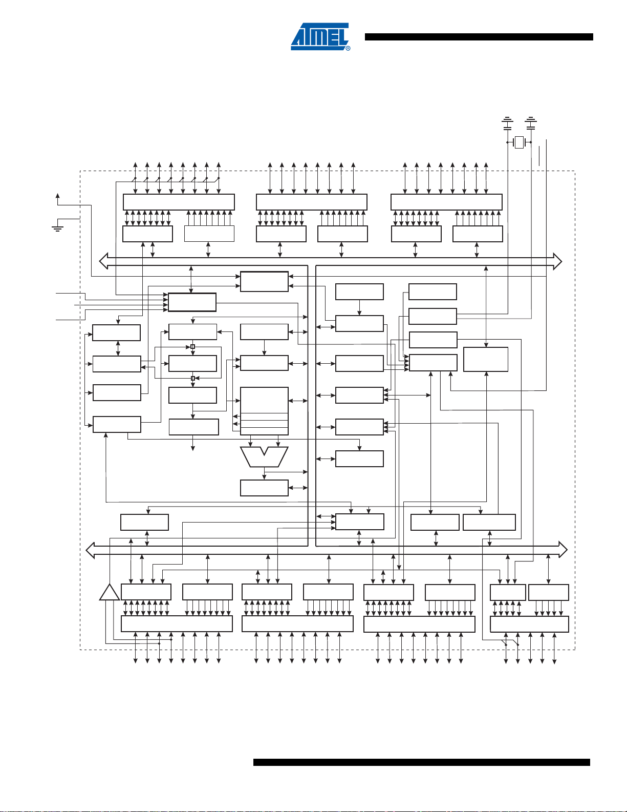
1.4 Block Diagram
Figure 1-1. Block Diagram
VCC
GND
AVCC
AGND
AREF
DATA REGISTER
JTAG TAP
ON-CHIP DEBUG
BOUNDARY-
SCAN
PROGRAMMING
LOGIC
PORTF DRIVERS
PORTF
DATA DIR.
REG. PORTF
ADC
PROGRAM
COUNTER
PROGRAM
FLASH
INSTRUCTION
REGISTER
INSTRUCTION
DECODER
DATA REGISTER
PORTA
POR - BOD
RESET
STACK
POINTER
SRAM
GENERAL
PURPOSE
REGISTERS
X
Y
Z
PA7 - PA0PF7 - PF0
PORTA DRIVERS
DATA DIR.
REG. PORTA
8-BIT DATA BUS
INTERNAL
OSCILLATOR
WATCHDOG
TIMER
MCU CONTROL
REGISTER
TIMER/
COUNTERS
INTERRUPT
UNIT
PORTC DRIVERS
DATA REGISTER
PORTC
CALIB. OSC
OSCILLATOR
OSCILLATOR
TIMING AND
CONTROL
PC7 - PC0
DATA DIR.
REG. PORTC
CAN
CONTROLLER
XTAL1
XTAL2
RESET
ANALOG
COMPARATOR
DATA REGISTER
+
-
PORTE
CONTROL
LINES
DATA DIR.
REG. PORTE
PORTE DRIVERS
ALU
STATUS
REGISTER
DATA REGISTER
PORTB
PORTB DRIVERS
PB7 - PB0PE7 - PE0
DATA DIR.
REG. PORTB
EEPROM
SPIUSART0
DATA REGISTER
PORTD
PORTD DRIVERS
PD7 - PD0
USART1
DATA DIR.
REG. PORTD
TWO-WIRE SERIAL
INTERFACE
DATA REG.
PORTG
DATA DIR.
REG. PORTG
PORTG DRIVERS
PG4 - PG0
4
7679F–CAN–11/07

1.5 Pin Configurations
Figure 1-2. Pinout AT90CAN32/64/128 - TQFP
AT90CAN32/64/128
NC
(RXD0 / PDI) PE0
(TXD0 / PDO) PE1
(XCK0 / AIN0) PE2
(OC3A / AIN1) PE3
(OC3B / INT4) PE4
(OC3C / INT5) PE5
(T3 / INT6) PE6
(ICP3 / INT7) PE7
(SS) PB0
(SCK) PB1
(MOSI) PB2
(MISO) PB3
(OC2A) PB4
(OC1A) PB5
(OC1B) PB6
AVCC
64
(1)
1
2
3
4
5
6
7
8
9
10
11
12
13
14
15
16
AREF
GND
62
63
INDEX CORNER
PF1 (ADC1)
PF0 (ADC0)
61
60
(64-lead TQFP top view)
PF3 (ADC3)
PF2 (ADC2)
592058
PF5 (ADC5 / TMS)
PF4 (ADC4 / TCK)
572256
PF6 (ADC6 / TDO)
VCC
GND
PF7 (ADC7 / TDI)
54
532652
PA0 (AD0)
PA1 (AD1)
51
50
PA2 (AD2)
49
48
47
46
45
44
43
42
41
40
39
38
37
36
35
34
33
PA3 (AD3)
PA4 (AD4)
PA5 (AD5)
PA6 (AD6)
PA7 (AD7)
PG2 (ALE)
PC7 (A15 / CLKO)
PC6 (A14)
PC5 (A13)
PC4 (A12)
PC3 (A11)
PC2 (A10)
PC1 (A9)
PC0 (A8)
PG1 (RD)
PG0 (WR)
7679F–CAN–11/07
17
18
19
(2)
(2)
(TOSC2 ) PG3
(TOSC1 ) PG4
(1)
NC = Do not connect (May be used in future devices)
(2)
Timer2 Oscillator
(OC0A / OC1C) PB7
21
VCC
RESET
GND
235524
XTAL2
25
XTAL1
(SCL / INT0) PD0
28
27
(SDA / INT1) PD1
(TXD1 / INT3) PD3
(RXD1 / INT2) PD2
29
(ICP1) PD4
31
30
(RXCAN / T1) PD6
(TXCAN / XCK1) PD5
32
(T0) PD7
5
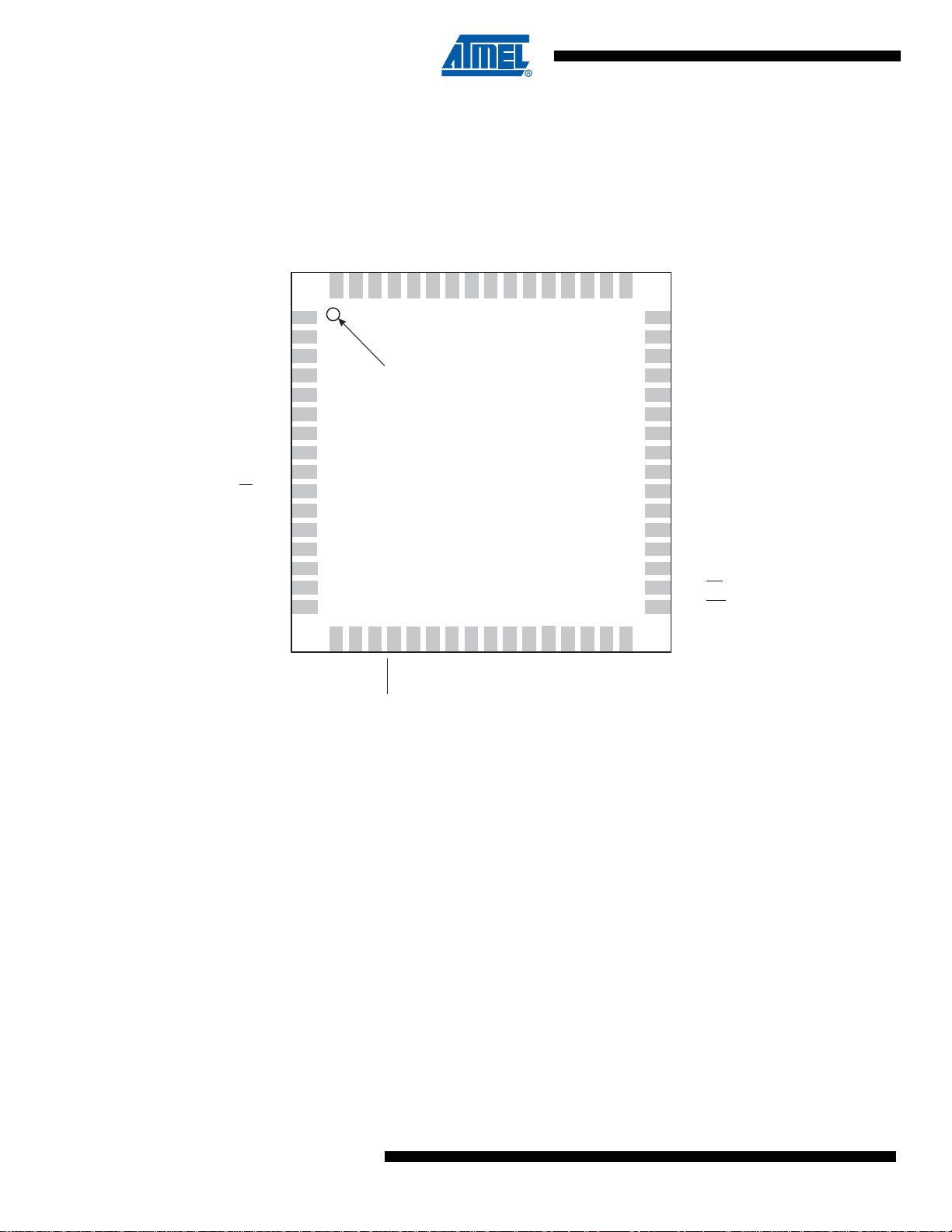
AT90CAN32/64/128
Figure 1-3. Pinout AT90CAN32/64/128 - QFN
AREF
GND
AVCC
6463625361
(1)
NC
1
(RXD0 / PDI) PE0
(TXD0 / PDO) PE1
(XCK0 / AIN0) PE2
(OC3A / AIN1) PE3
(OC3B / INT4) PE4
(OC3C / INT5) PE5
(T3 / INT6) PE6
(ICP3 / INT7) PE7
(SS) PB0
(SCK) PB1
(MOSI) PB2
(MISO) PB3
(OC2A) PB4
(OC1A) PB5
(OC1B) PB6
2
3
4
5
6
7
8
9
10
11
12
13
14
15
16 33
(64-lead QFN top view)
PF0 (ADC0)
PF1 (ADC1)
PF2 (ADC2)
PF3 (ADC3)
605958
INDEX CORNER
GND
PF4 (ADC4 / TCK)
575655
PF7 (ADC7 / TDI)
PF5 (ADC5 / TMS)
PF6 (ADC6 / TDO)
54
VCC
PA0 (AD0)
525150
PA1 (AD1)
PA2 (AD2)
49
46
PA3 (AD3)
48
PA4 (AD4)
47
PA5 (AD5)
PA6 (AD6)
45
PA7 (AD7)
44
PG2 (ALE)
43
PC7 (A15 / CLKO)
42
PC6 (A14)
41
PC5 (A13)
40
PC4 (A12)
39
PC3 (A11)
38
PC2 (A10)
37
PC1 (A9)
36
PC0 (A8)
35
PG1 (RD)
34
PG0 (WR)
(1)
NC = Do not connect (May be used in future devices)
(2)
Timer2 Oscillator
Note: The large center pad underneath the QFN package is made of metal and internally connected to
1.6 Pin Descriptions
1.6.1 VCC
Digital supply voltage.
1.6.2 GND
Ground.
17
182019
(2)
(TOSC2 ) PG3
(OC0A / OC1C) PB7
21222324252627
VCC
(2)
RESET
(TOSC1 ) PG4
GND
XTAL1
XTAL2
(SCL / INT0) PD0
28
29
30
(ICP1) PD4
(SDA / INT1) PD1
(TXD1 / INT3) PD3
(RXD1 / INT2) PD2
(TXCAN / XCK1) PD5
32
31
(T0) PD7
(RXCAN / T1) PD6
GND. It should be sold ered or g lued to the boar d to ens ure good mech anica l st abili ty. If the center
pad is left unconnected, the package might loosen from the board.
6
7679F–CAN–11/07

1.6.3 Port A (PA7..PA0)
Port A is an 8-bi t b i- dire ctional I/O port with internal pull-up res is tors ( sele cte d f or ea ch bi t). T h e
Port A output buffers have symmetrical drive characteristics with both high sink and source
capability. As inputs, Port A pins that are externally pulled low will source current if the pull-up
resistors are activated. The Port A pins are tri-stated whe n a rese t condition bec omes ac tive,
even if the clock is not running.
Port A also serves the funct ions of variou s specia l features of t he AT90CAN32/ 64/128 as list ed
on page 74.
1.6.4 Port B (PB7..PB0)
Port B is an 8-bi t b i- dire ctional I/O port with internal pull-up res is tors ( sele cte d f or ea ch bi t). T h e
Port B output buffers have symmetrical drive characteristics with both high sink and source
capability. As inputs, Port B pins that are externally pulled low will source current if the pull-up
resistors are activated. The Port B pins are tri-stated whe n a rese t condition bec omes ac tive,
even if the clock is not running.
Port B also serves the funct ions of variou s specia l features of t he AT90CAN32/ 64/128 as list ed
on page 76.
1.6.5 Port C (PC7..PC0)
Port C is an 8-bit bi-directional I/O port with internal pull-up resistors (selected for each bit). The
Port C output buffers have symmetrical drive characteristics with both high sink and source
capability. As inputs, Port C pins that are externally pulled low will source current if the pull-up
resistors are activated. The Port C pi ns are tri-stated when a res et condition bec omes active,
even if the clock is not running.
AT90CAN32/64/128
Port C also serves the functions of special features of the AT90CAN32/64/128 as listed on page
78.
1.6.6 Port D (PD7..PD0)
Port D is an 8-bit bi-directional I/O port with internal pull-up resistors (selected for each bit). The
Port D output buffers have symmetrical drive characteristics with both high sink and source
capability. As inputs, Port D pins that are externally pulled low will source current if the pull-up
resistors are activated. The Port D pi ns are tri-stated when a res et condition bec omes active,
even if the clock is not running.
Port D also serves the fu nction s of v arious speci al feat ures of the AT90CAN 32/6 4/128 a s li sted
on page 80.
1.6.7 Port E (PE7..PE0)
Port E is an 8-bi t b i- dire ctional I/O port with internal pull-up res is tors ( sele cte d f or ea ch bi t). T h e
Port E output buffers have symmetrical drive characteristics with both high sink and source
capability. As inputs, Port E pins that are externally pulled low will source current if the pull-up
resistors are activated. The Port E pins are tri-stated whe n a rese t condition bec omes ac tive,
even if the clock is not running.
Port E also serves the funct ions of variou s specia l features of t he AT90CAN32/ 64/128 as list ed
on page 83.
1.6.8 Port F (PF7..PF0)
Port F serves as the analog inputs to the A/D Converter.
7679F–CAN–11/07
7

AT90CAN32/64/128
Port F also serves as an 8-bit bi-directional I/O port, if the A/D Converter is not used. Port pins
can provide internal pull-up resistors (selected for each bit). The Port F output buffers have symmetrical drive charac teristics wi th both hig h sink and source capabili ty. As inp uts, Port F pins
that are externall y pu ll ed low wi ll sour c e cu rren t i f th e pul l- up re sis tors ar e ac tivated. The Port F
pins are tri-stated when a reset condition becomes active, even if the clock is not running.
Port F also serves the functions of the JTAG interface. If the JTAG interface is enabled, the pullup resistors on pins PF7(TDI), PF5(TMS), and PF4(TCK) will be activated even if a reset occurs.
1.6.9 Port G (P G 4 .. P G 0 )
Port G is a 5-bit I/O p ort wi th inte rnal pul l-up resisto rs (s elect ed for eac h bit) . The Po rt G o utput
buffers have symmetrical drive characteristics with both high sink and source capabil ity. As
inputs, Port G pins that are externally pulled low will source current if the pul l-up resistors are
activated. The Port G pins are tri-stated when a reset condition becomes active, even if the clock
is not running.
Port G also serves th e funct ions o f va rious s peci al featu res of the AT90C AN32 /64/128 as li sted
on page 88.
1.6.10 RESET
1.6.11 XTAL1
1.6.12 XTAL2
1.6.13 AVCC
1.6.14 AREF
Reset input. A low level on this pin for longer than the minimum pulse length will generate a
reset. The minimum pulse length is given in characteristics. Shorter pulses are not guaranteed
to generate a reset. The I/O ports of the AVR are immediately reset to their initial state even if
the clock is not running. The clock is needed to reset the rest of the AT90CAN32/64/128.
Input to the inverting Oscillator amplifier and input to the internal clock operating circuit.
Output from the inverting Oscillator amplifier.
AVCC is the supply voltage pin for the A/D Converter on Port F. It should be externally connected to V
through a low-pass filter.
This is the analog reference pin for the A/D Converter.
CC
2. About Code Examples
This documentation contains simple code examples that briefly show how to use various parts of
the device. These code examples assume that the part specific header file is inc luded before
compilation. Be aware that not all C compiler vendors include bit definitions in the header files
and interrupt handling in C is compiler dependent. Please confirm with the C compiler documentation for more details.
, even if the ADC is not used. If the ADC is used, it should be connected to V
CC
8
7679F–CAN–11/07
3. AVR CPU Core
3.1 Introduction
This section discusses the AVR core architecture in general. The main function of the CPU core
is to ensure correct program execution. The CPU must therefore be able to access memories,
perform calculations, control peripherals, and handle interrupts.
3.2 Architectural Overview
Figure 3-1. Block Diagram of the AVR Architecture
AT90CAN32/64/128
Data Bus 8-bit
Flash
Program
Memory
Instruction
Register
Instruction
Decoder
Control Lines
Program
Counter
Direct Addressing
Status
and Control
32 x 8
General
Purpose
Registrers
ALU
Indirect Addressing
Data
SRAM
EEPROM
Interrupt
Unit
SPI
Unit
Watchdog
Timer
Analog
Comparator
I/O Module1
I/O Module 2
I/O Module n
7679F–CAN–11/07
I/O Lines
In order to maximize performance and parallelism, the AVR uses a Harvard architecture – with
separate memories and buse s for program and data. Instructi ons in the p rogram memory ar e
executed with a single level pipelining. While one instruction is being executed, the next instruction is pre-fetched from the p rogram memory . This concep t enabl es i nstruct ions to be ex ecute d
in every clock cycle. The program memory is In-System Reprogrammable Flash memory.
9

AT90CAN32/64/128
The fast-access Register File contains 32 x 8-bit general purpose working registers with a single
clock cycle access time. This allows single-cycle Arithmetic Logic Unit (ALU) operation. In a typical ALU operation, two operands are output from the Register File, the operation is executed,
and the result is stored back in the Register File – in one clock cycle.
Six of the 32 r egisters can be used as three 1 6-bit i ndirect address register pointer s for Dat a
Space addressing – enabling efficient address calculations. One of the these address pointers
can also be used as an address pointer for look up tables in Flash program memory. These
added function registers are the 16-bit X-, Y-, and Z-register, described later in this section.
The ALU supports ar it hme tic a nd log ic o perati on s betwe en r egisters or between a co ns tan t an d
a register. Single register operations can also be executed in the ALU. After an arithmetic operation, the Status Register is updated to reflect information about the result of the operation.
Program flow is provided by conditional and unconditional jump and call instructions, able to
directly address the whol e addres s space. Mo st AVR instru ctions hav e a single 16 -bit word format. Every program memory address contains a 16- or 32-bit instruction.
Program Flash memory space is divided in two sections, the Boot Program sec tion and the
Application Prog ram sect ion. Both se ctions ha ve dedicate d Lock bits for write and rea d/write
protection. The SPM (Store Program Memory) instruction that writes into the Application Flash
memory section must reside in the Boot Program section.
During interrupts and subroutine calls, the return address Program Counter (PC) is stored on the
Stack. The Stack is e ffec ti ve ly al lo ca ted in the general data SR A M, a nd co nse que ntl y the Sta ck
size is only limited by th e total SRAM size a nd the usage of the SRAM . All user p rogram s mus t
initialize the SP in th e Re set routi ne (bef ore s ubrou tine s o r int errup ts are e xecut ed ). The Sta ck
Pointer (SP) is read/write accessible in the I/O space. The data SRAM can easily be accessed
through the five different addressing modes supported in the AVR architecture.
The memory spaces in the AVR architecture are all linear and regular memory maps.
A flexible inter rupt modul e has its cont rol registe rs in the I/O s pace with a n additional Global
Interrupt Enable bit in the Status Register. All interrupts have a separate Interrupt Vector in the
Interrupt Vector table. T he in terr up ts h av e pri or ity in ac co rd ance wi th t hei r Interr up t Ve cto r pos ition. The lower the Interrupt Vector address, the higher is the priority.
The I/O memory space contains 64 addresses for CPU peripheral functions as Control Registers, SPI, and other I/O functions. The I/O Memory can be accessed directly, or as the Data
Space locations following those of the Register File, 0x20 - 0x5F. In addition, the
AT90CAN32/64/128 has Extended I/O space from 0x60 - 0xFF in SRAM where only the
ST/STS/STD and LD/LDS/LDD instructions can be used.
3.3 ALU – Arithmetic Logic Unit
The high-performance AVR ALU operates in direct connection with all the 32 general purpose
working registers. Within a single c lock cycle, arithmetic operat ions between general purpose
registers or between a register and an immediate are executed. The ALU operations are divided
into three main categories – arithmetic, logical, and bit-functions. Some implementations of the
architecture also provide a po werful mult iplier suppo rting both sig ned/unsig ned multipl ication
and fractional format. See the “Instruction Set Summary” section for a detailed description.
10
7679F–CAN–11/07

3.4 Status Register
AT90CAN32/64/128
The Status Register contains information about the result of the m ost recently exe cuted arithmetic instruction. This information can be used for altering program flow in order to perform
conditional operations. Note that the Status Register is updated after all ALU operations, as
specified in the Instruction Set Reference. This will in many cases remove the need for using the
dedicated compare instructions, resulting in faster and more compact code.
The Status Re gis ter i s no t au tomat icall y s tored w hen enteri ng a n in ter rupt routi ne a nd r estor ed
when returning from an interrupt. This must be handled by software.
The AVR Status Register – SREG – is defined as:
Bit 76543210
I T H S V N Z C SREG
Read/Write R/W R/W R/W R/W R/W R/W R/W R/W
Initial Value00000000
• Bit 7 – I: Global Interrupt Enable
The Global Interrupt Enable bit must be set to enable d the interrupts. The in dividual interru pt
enable control is then performed in separate control registers. If the Global Interrupt Enable
Register is cleared, none of the interrupts are ena bled independ ent of the individual interrupt
enable settings. The I-bit is cleared by hardware after an interrupt has occurred, and is set by
the RETI instruction to enable subsequent interrupts. The I-bit can also be set and cleared by
the application with the SEI and CLI instructions, as described in the instruction set reference.
• Bit 6 – T: Bit Copy Storage
The Bit Copy instr uctions BL D (Bit LoaD) and BST (B it STore) us e the T-bit as source or destination for the operated bit. A bit from a register in the Register File can be copied into T by the
BST instruction, and a bit in T can be copied into a bit in a regi ster in the Register File by the
BLD instruction.
• Bit 5 – H: Half Carry Flag
The Half Carry Flag H ind icate s a Hal f Carry in s ome ari thmetic operati ons. Ha lf Carry Is usefu l
in BCD arithmetic. See the “Instruction Set Description” for detailed information.
• Bit 4 – S: Sign Bit, S = N
⊕ V
The S-bit is always an EXCLUSIVE OR between the negative flag N and the Two’s Complement
Overflow Flag V. See the “Instruction Set Description” for detailed information.
• Bit 3 – V: Two’s Complement Overflow Flag
The Two’s Complement Overflow Flag V supports two’s complement arithmetics. See the
“Instruction Set Description” for detailed information.
• Bit 2 – N: Negative Flag
The Negative Flag N indicates a negative result in an arithmetic or logic operation. See the
“Instruction Set Description” for detailed information.
• Bit 1 – Z: Zero Flag
The Zero Flag Z indicates a zero result in an arithmetic or logic operation. See the “Instruction
Set Description” for detailed information.
7679F–CAN–11/07
11

AT90CAN32/64/128
• Bit 0 – C: Carry Flag
The Carry Flag C indicates a carry in an arithmetic or logic operation. See the “Instruction Set
Description” for detailed information.
3.5 General Purpose Register File
The Register File is optimized for the AVR Enhanced RISC instruction set. In order to achieve
the required performance and flexibility, the following input/output schemes are supported by the
Register File:
• One 8-bit output operand and one 8-bit result input
• Two 8-bit output operands and one 8-bit result input
• Two 8-bit output operands and one 16-bit result input
• One 16-bit output operand and one 16-bit result input
Figure 3-2 shows the structure of the 32 general purpose working registers in the CPU.
Figure 3-2. AVR CPU General Purpose Working Registers
General R14 0x0E
Purpose R15 0x0F
Working R16 0x10
Registers R17 0x11
70Addr.
R0 0x00
R1 0x01
R2 0x02
…
R13 0x0D
…
R26 0x1A X-register Low Byte
R27 0x1B X-register High Byte
R28 0x1C Y-register Low Byte
R29 0x1D Y-register High Byte
R30 0x1E Z-register Low Byte
R31 0x1F Z-register High Byte
Most of the instructions operati ng on the Regis ter File have d irect access to all register s, and
most of them are single cycle instructions.
As shown i n Figure 3-2, each register is also assigned a data memory address, mapping them
directly into the first 32 locations of the user Data Space. Although not being physically implemented as SRAM locations, this memory organization provides great flexibility in access of the
registers, as the X-, Y- and Z-pointer registers can be set to index any register in the file.
3.5.1 The X-register, Y-register, and Z-register
The registers R26..R31 have s ome adde d functi ons to their gen eral purpose us age. Thes e registers are 16-bit address poin ters for indirec t addressing of the data space. The three indi rect
address registers X, Y, and Z are defined as des cri bed in Figure 3-3.
12
7679F–CAN–11/07
Figure 3-3. The X-, Y-, and Z-registers
15 XH XL 0
X-register 7 0 7 0
R27 (0x1B) R26 (0x1A)
15 YH YL 0
Y-register 7 0 7 0
R29 (0x1D) R28 (0x1C)
15 ZH ZL 0
Z-register 7 0 7 0
R31 (0x1F) R30 (0x1E)
In the different addressing modes these address registers have functions as fixed displacement,
automatic increment, and automatic decrement (see the instruction set reference for details).
3.5.2 Extended Z-pointer Register for ELPM/SPM – RAMPZ
Bit 7 6 5 4 3 2 1 0
– – – – – – – RAMPZ0 RAMPZ
Read/Write R R R R R R R R/W
Initial Value 0 0 0 0 0 0 0 0
AT90CAN32/64/128
• Bits 7..1 – Res: Reserved Bits
These bits are reserved for fut ur e us e an d will a lwa ys read a s z ero. F or comp ati bil it y wi th fu tur e
devices, be sure to write to write them to zero.
• Bit 0 – RAMPZ0: Extended RAM Page Z-pointer
The RAMPZ Register is normally us ed to select whi ch 64K RAM Page is accesse d by the Zpointer. As the AT90CAN32/64/128 does not support more than 64K of SRAM memory, this register is used only to select which page in the program memory is accessed when the ELPM/SPM
instruction is used. The different settings of the RAMPZ0 bit have the following effects:
RAMPZ0 = 0:Program memory address 0x0000 - 0x7FFF (lower 64K bytes) is accessed by
ELPM/SPM
RAMPZ0 = 1:Program memory address 0x8000 - 0xFFFF (higher 64K bytes) is accessed by
ELPM/SPM
– AT90CAN32 and AT90CAN64: RAMPZ0 exists as registe r bit but it is not used for
program memory addressing.
– AT90CAN128: RAMPZ0 exists as register bit and it is used for program memory
addressing.
Figure 3-4. The Z-pointer used by ELPM and SPM
7Bit (Individually) 0 7 0 7 0
RAMPZ ZH ZL
23Bit (Z-pointer) 16 15 8 7 0
7679F–CAN–11/07
Note: LPM (different of ELPM) is never affected by the RAMPZ setting.
13
AT90CAN32/64/128
3.6 Stack Pointer
The Stack is mainly used for storing temporary data, for storing local variables and for storing
return addresses aft er interrupts and subroutin e c all s . The S ta ck Po in ter Reg ister al ways poi nts
to the top o f t he S t ac k. N ot e t h at t h e S tack is implemente d a s gr ow i ng f ro m hi gh e r m em or y l o ca tions to lower memory locations. This implies that a Stack PUSH command decreases the Stack
Pointer.
The Stack Point er points to the data SRAM S tack area wh ere the Su broutine a nd Interrupt
Stacks are located. Thi s Stac k space i n the data S RAM mus t be defin ed by the pr ogram be fore
any subroutine calls are executed or interrupts are enabled. The Stack Pointer must be s et to
point above 0xFF. The Stack Pointer is decremented by one when data is pushed onto the Stack
with the PUSH instruction, and it is decremented by two when the return address is pushed onto
the Stack with subroutine call or interrupt. The Stack Pointer is incremented by one when data is
popped from the Stack w ith the POP instruction, and it is incr emented by two when data is
popped from the Stack with return from subroutine RET or return from interrupt RETI.
The AVR Stack Pointer is implemented as two 8-bit registers in the I/O space. The number of
bits actually used is implementation dependent. Note that the data space in some implementations of the AVR architecture is so small that only SPL is needed. In this case, the SPH Register
will not be present.
Bit 151413121110 9 8
SP15 SP14 SP13 SP12 SP11 SP10 SP9 SP8 SPH
SP7 SP6 SP5 SP4 SP3 SP2 SP1 SP0 SPL
76543210
Read/Write R/W R/W R/W R/W R/W R/W R/W R/W
R/W R/W R/W R/W R/W R/W R/W R/W
Initial Value 00 000000
00000000
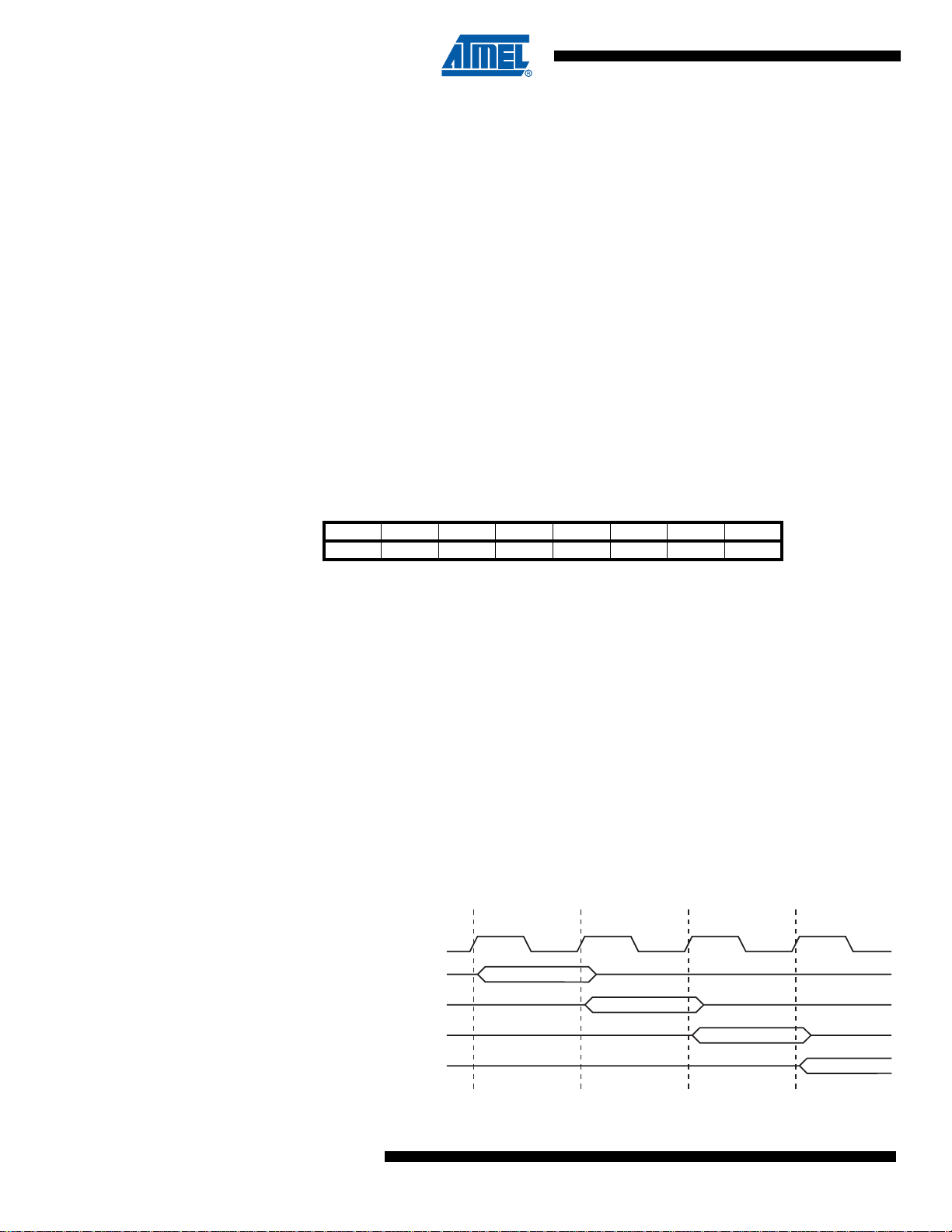
3.7 Instruction Execution Timing
This section describes the general access timing concepts for instruction execution. The AVR
CPU is driven by the CPU clock clk
chip. No internal clock division is used.
Figure 3-5 shows the parallel instructio n fetches an d instruc tion ex ecutions enable d by the Ha r-
vard architecture and th e fast- access Register File con cept. Thi s is the bas ic pipel ining conce pt
to obtain up to 1 MIPS per MHz with the cor respondi ng unique res ults for func tions per cos t,
functions per clocks, and functions per power-unit.
Figure 3-5. The Parallel Instruction Fetches and Instruction Executions
1st Instruction Fetch
1st Instruction Execute
2nd Instruction Fetch
2nd Instruction Execute
3rd Instruction Fetch
3rd Instruction Execute
4th Instruction Fetch
clk
CPU
, directly generated from the selected clock source for the
CPU
T1 T2 T3 T4
14
7679F–CAN–11/07
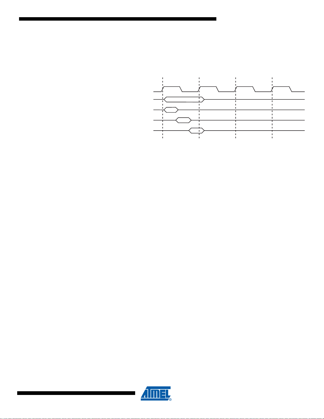
Figure 3- 6 shows the internal timing concept for the Register File. In a single clock cycle an ALU
operation using two regi ster ope rands is executed , and the result is stored bac k to the de stination register.
Figure 3-6. Single Cycle ALU Operation
Total Execution Time
Register Operands Fetch
ALU Operation Execute
Result Write Back
3.8 Reset and Interrupt Handling
The AVR provides several different interrupt sources. These interrupts and the separate Reset
Vector each have a separate program vector in the program memory space. All interrupts ar e
assigned individual enable bits which must be written logic one together with the Global Interrupt
Enable bit in the Status Re gister in or der to ena ble the int errupt. De pendin g on the Prog ram
Counter value, interrupts may be automatically disabled when Boot Lock bits BLB02 or BLB12
are programmed. This feature improves software security. See the section “Memory Program-
ming” on page 336 for details .
clk
AT90CAN32/64/128
T1 T2 T3 T4
CPU
The lowest addresses in the p rogram memory space are by default defined as the Reset a nd
Interrupt Vectors. The complete list of vectors is shown in “Interrupts” on pag e 60. The list also
determines the priority levels of the different interrupts. The lower the address the higher is the
priority level. RESE T has the highe st priorit y, and next is INT 0 – the External Interrupt Requ est
0. The Interrupt Vectors can be moved to the start of the Boot Flash section by setting the IVSEL
bit in the MCU Control Register (MCUCR). Refer to “Interrupts” on page 60 for more information.
The Reset Vector can also be m oved to the s tart o f the Bo ot Flas h secti on by p rogram ming th e
BOOTRST Fu se, s ee “Boot Loader Support – Read-While-Write Self-Programming” on page
321.
3.8.1 Interrupt Behavior
When an interrupt occurs, the Global Interrupt Enable I-bit is cleared and all interrupts are disabled. The user softw are c an write lo gic one to the I-bit to enab le nes ted i nterrup ts. Al l ena bled
interrupts can then interrupt the current interrupt routine. The I-bit is automa tically set when a
Return from Interrupt instruction – RETI – is executed.
There are basically two types of interrupts. The first type is triggered by an event that sets the
interrupt flag. For these interrupts, the Program Counter is vectored to the actual Interrupt Vector
in order to execut e the int errupt ha ndlin g routine , and hardware clears the cor respon ding inte rrupt flag. Interrupt flags can also be cleared by writing a logic one to the flag bit position(s) to be
cleared. If an interrupt condition occurs while the corresponding interrupt enable bit is cleared,
the interrupt flag wi ll be set an d remembe red u ntil th e interr upt is enabl ed, or th e flag is c leared
by software. Similarly, if one or more interrupt conditions occur while the Global Interrupt Enable
bit is cleared, the c orrespond ing interru pt flag(s) wil l be set and reme mbered unti l the Globa l
Interrupt Enable bit is set, and will then be executed by order of priority.
7679F–CAN–11/07
15

AT90CAN32/64/128
The second type of interrupts will trigger as long as the interrupt condition is present. These
interrupts do not necessa rily hav e in ter rupt fl ags . If the interr up t con dit ion disapp ear s befo re the
interrupt is enabled, the interrupt will not be triggered.
When the AVR exits from an interrupt, it will always return to the main program and execute one
more instruction before any pending interrupt is served.
Note that the Status Register is not automatic ally stored when entering an in terrupt rou tine, nor
restored when returning from an interrupt routine. This must be handled by software.
When using the CLI instruct ion to disable interrupts, the interrupt s will be immedia tely disab led.
No interrupt will be executed after the CLI instruction, even if it occurs simultaneously with the
CLI instruction. The following example shows how this can be used to avoid interrupts during the
timed EEPROM write sequence.
Assembly Code Example
in r16, SREG ; store SREG value
cli ; disable interrupts during timed sequence
sbi EECR, EEMWE ; start EEPROM write
sbi EECR, EEWE
out SREG, r16 ; restore SREG value (I-bit)
C Code Example
char cSREG;
cSREG = SREG; /* store SREG value */
/* disable interrupts during timed sequence */
_CLI();
EECR |= (1<<EEMWE); /* start EEPROM write */
EECR |= (1<<EEWE);
SREG = cSREG; /* restore SREG value (I-bit) */
When using the SEI instruction to enable interrupts, the instruction following SEI will be executed before any pending interrupts, as shown in this example.
Assembly Code Example
sei ; set Global Interrupt Enable
sleep ; enter sleep, waiting for interrupt
; note: will enter sleep before any pending
; interrupt(s)
C Code Example
_SEI(); /* set Global Interrupt Enable */
_SLEEP(); /* enter sleep, waiting for interrupt */
/* note: will enter sleep before any pending interrupt(s) */
16
7679F–CAN–11/07

3.8.2 Interrupt Response Time
The interrupt execution response for all the enabled AVR interrupts is four clock cycles minimum. After four clock cycles the program vector address for the actual interrupt handling routine
is executed. During this four clock cycle pe riod , the Prog ram Co unter is pu shed o nto the Stack.
The vector is normally a jump to the interrupt routine, and this jump takes three clock cycles. If
an interrupt occurs during execution of a multi-cycle instruction, this instruction is completed
before the interrupt is served. If an interrupt occurs when the MCU is in sleep mode, the interrupt
execution response time is increased by four clock cycles. This increase comes in addition to the
start-up time from the selected sleep mode.
A return from an inter rupt handli ng routine takes four clock cycles. During the se four c lock
cycles, the Program Cou nter (two bytes ) is popped back fr om the Stack, the Sta ck Pointer is
incremented by two, and the I-bit in SREG is set.
AT90CAN32/64/128
7679F–CAN–11/07
17

AT90CAN32/64/128
4. Memories
This section describes th e di ffe re nt m emo ries in the A T90CA N32 /64/1 28. T he A V R arc hit ect ur e
has two main memory spaces, the Data Memory and the Program Memory space. In addition,
the AT90CAN32/64/128 features an EEPROM Memory for data storage. All three memory
spaces are linear and regular.
Table 4-1. Memory Mapping.
Memory Mnemonic AT90CAN32 AT90CAN64 AT90CAN128
Flash
32
Registers
I/O
Registers
Ext I/O
Registers
Internal
SRAM
External
Memory
EEPROM
Size
Start Address
End Address
Size
Start Address
End Address
Size
Start Address
End Address
Size
Start Address
End Address
Size
Start Address
End Address
Size
Start Address
End Address
Size
Start Address
End Address
Flash size 3 2 K bytes 64 K bytes 128 K bytes
- 0x00000
Flash end
0x07FFF
0x3FFF
(1)
(2)
0x0FFFF
0x7FFF
(1)
(2)
0x1FFFF
0xFFFF
(1)
(2)
-32 bytes
- 0x0000
- 0x001F
-64 bytes
- 0x0020
- 0x005F
- 160 bytes
- 0x0060
-0x00FF
ISRAM size 2 K bytes 4 K bytes 4 K bytes
ISRAM start 0x0100
ISRAM end 0x08FF 0x10FF 0x10FF
XMem size 0-64 K bytes
XMem start 0x0900 0x1100 0x1100
XMem end 0xFFFF
E2 size 1 K bytes 2 K bytes 4 K bytes
- 0x0000
E2 end 0x03FF 0x07FF 0x0FFF
Notes: 1. Byte address.
4.1 In-System Reprogrammable Flash Program Memory
The AT90CAN32/64/128 contains On-chip In-System Reprogrammable Flash memory for program storage (see “Flash size”). Since all AVR instructions are 16 or 32 bits wide, the Flash is
organized as 16 bits wide. For software security, the Flash Program memory space is divided
into two sections, Boot Program section and Application Program section.
The Flash memory has an endurance of at least 10,000 write/erase cycles. The
AT90CAN32/64/128 Program Counter (PC) address the program memory locations. The operation of Boot Program section and associated Boot Lock bits for software protection are described
in detail in “Boot Loader Support – Read-While-Write Self-Programming” on page 321. “Memory
Programming” on pa ge 336 contai ns a detailed de scription on Flash data ser ial download ing
using the SPI pins or the JTAG interface.
18
2. Word (16-bit) address.
7679F–CAN–11/07

AT90CAN32/64/128
Constant tables can be allocated within the entire program memory address space (see the
LPM – Load Program Memory and ELPM – Extended Load Program Memory instruction
description).
Timing diagrams for instruction fetch and execution are presented in “Instruction Execution Tim-
ing” on page 14.
Figure 4-1. Program Memory Map
Program Memory
0x0000
Application Flash Section
4.2 SRAM Data Memory
Figure 4-2 shows how the AT90CAN32/64/128 SRAM Memory is organized.
The AT90CAN32/6 4/128 i s a c omplex microc ontroller with m ore pe ripheral u nits t han can be
supported within the 64 locations reserved in the Opcode for the IN and OUT instructions. For
the Extended I/O space in SRAM, only the ST/STS/STD and LD/LDS/LDD instructions can be
used.
The lower data memory loc ati ons add re ss bo th the Register File, the I/O memor y, E xte nde d I/O
memory, and the internal data SRAM. The first 32 locations address the Register File, the next
64 location the standar d I/O memo ry, then 1 60 loca tions of Extended I/O mem ory, and the next
locations address the internal data SRAM (see “ISRAM size”).
An optional external data SRAM can be used with the AT90CAN32/64/128. T his SRAM will
occupy an area in the remaining address locations in the 64K address space. This area starts at
the address following the internal SRAM. The Register file, I/O, Extended I/O and Internal SRAM
occupies the lowest bytes , so when using 64 KB (65,536 bytes) of External Memory,
“XMem size” bytes of Exter nal Me mory ar e availab le. See “Exter nal Me mory Interfa ce” o n page
27 for details on how to take advantage of the external memory map.
Boot Flash Section
Flash end
7679F–CAN–11/07
19

AT90CAN32/64/128
4.2.1 SRAM Data Access
When the addresses ac cessing the SRA M memory spac e exceeds the internal data me mory
locations, the external data SRAM is acces sed using the sa me instructi ons as for the internal
data memory access. When the internal data memories are accessed, the read and write strobe
pins (PG0
enabled by setting the SRE bit in the XMCRA Register.
Accessing exte rnal SRA M takes one additi onal c lock cycl e per byte compar ed to ac cess of th e
internal SRAM. This means that the commands LD, ST, LDS, STS, LDD, STD, PUSH, and POP
take one additional clock cycle. If the Stack is placed in external SRAM, interrupts, subroutine
calls and returns take three clock cy cles ex tra bec aus e the two- byte pr og ra m cou nter i s pushe d
and popped, and external memory access does not take advantage of the internal pipe-line
memory access. When external SRAM interface is used with wait-state, one-byte external
access takes two, three, or four additional clock cycles for one, two, and three wait-states
respectively. Interrupts, subroutine calls and returns will need five, seven, or nine clock cycles
more than specified in the instruction set manual for one, two, and three wait-states.
The five different addressing modes for the data memory cover: Direct, Indirect with Displacement, Indirect, Ind irect with Pre- decrement , and Indirect with Post-inc rement. In the Re gister
File, registers R26 to R31 feature the indirect addressing pointer registers.
The direct addressing reaches the entire data space.
The Indirect with Displacement mode reaches 63 address locations from the base address given
by the Y- or Z-register.
and PG1) are inacti ve during th e whole access cycle. Exter nal SRAM oper ation is
When using register indirect addressing modes with automatic pre-decr ement and post-increment, the address registers X, Y, and Z are decremented or incremented.
The 32 general purpose working registers, 64 I/O Registers, 160 Extended I/O Registers, and
the “ISRAM size” bytes of internal data SRAM in the AT90CAN32/64/128 are all accessible
through all these add ress ing m odes. Th e Re gister F ile is desc ribed i n “Gener al P urpose R egis-
ter File” on page 12.
20
7679F–CAN–11/07
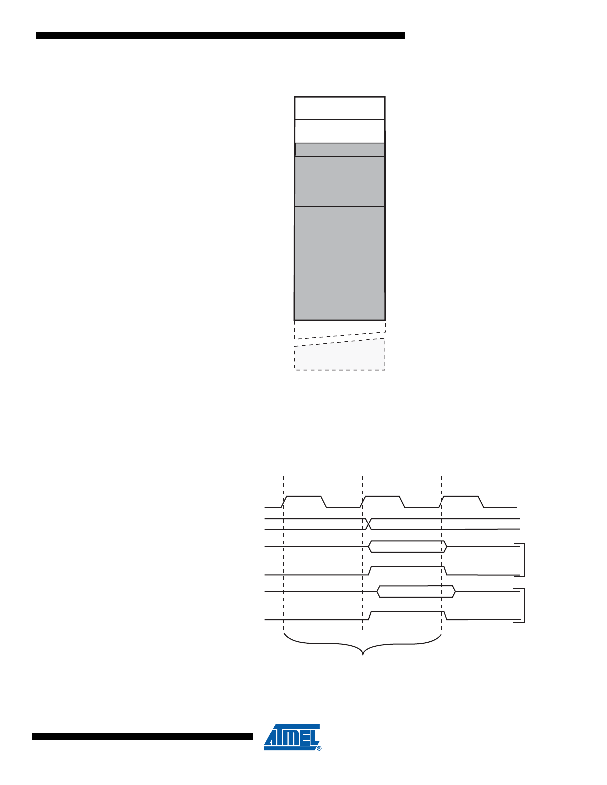
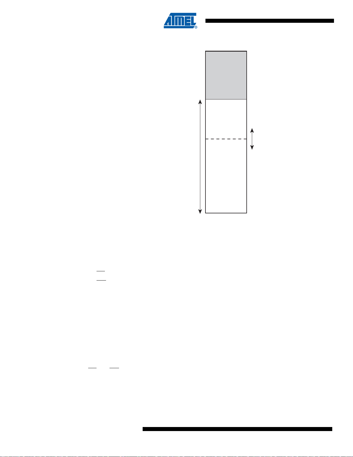
Figure 4-2. Data Memory Map
AT90CAN32/64/128
Data Memory
4.2.2 SRAM Data Access Times
This section describes the general access timing concepts for internal memory access. The
internal data SRAM access is performed in two clk
32 Registers
64 I/O Registers
160 Ext I/O Reg.
Internal SRAM
(ISRAM size)
External SRAM
(XMem size)
0x0000 - 0x001F
0x0020 - 0x005F
0x0060 - 0x00FF
ISRAM start
ISRAM end
XMem start
0xFFFF
cycles as described in Figure 4-3.
CPU
7679F–CAN–11/07
Figure 4-3. On-chip Data SRAM Access Cycles
T1 T2 T3
clk
CPU
Address
Compute Address
Data
WR
Data
RD
Memory Access Instruction
Address valid
Write
Read
Next Instruction
21

AT90CAN32/64/128
4.3 EEPROM Data Memory
The AT90CAN32/64/128 con tains EEPRO M memory (see “ E2 size”). It is organ ized as a separate data space, in which single bytes can be read and written. The EEPROM has an endurance
of at least 100,000 write/erase cycles. The access between the EEPROM and the CPU is
described in the following, specifying the EEPROM Address Registers, the EEPROM Data Register, and the EEPROM Control Registe r.
For a detailed description of SPI, JTAG and Parallel data downloading to the EEPROM, see
“SPI Serial Programming Overview” on page 348, “JTAG Programming Overview” on page 352,
and “Parallel Program mi ng Overv iew ” on page 339 respectively.
4.3.1 EEPROM Read/Write Access
The EEPROM Access Registers are accessible in the I/O space.
The write access time for the EEPROM is given in Table 4-2. A self-timing function, however,
lets the user software detect when the next byte can be written. If the user code contains instructions that write the EE PROM, some precau tions must be taken. In he avily filtered power
supplies, V
period of time to run at a vo ltag e lo wer tha n sp ec ifi ed as mi ni mum for the clo ck frequ enc y u se d.
See “Preventing EEPROM Corruption” on page 26.for details on how to avoid problems in these
situations.
In order to prevent unintentional EEPROM writes, a specific write procedure must be followed.
Refer to the description of the EEPROM Control Register for details on this.
CC
is likely to rise or fall slowly on power-up/down. This causes the device for some
When the EEPROM is read, the CPU is halted for four clock cycles before the next instruction is
executed. When the E EPROM is writ ten, the CPU i s halted for tw o clock cycles before t he nex t
instruction is execute d.
4.3.2 The EEPROM Address Registers – EEARH and EEARL
Bit 15 14 13 12 11 10 9 8
– – – – EEAR11 EEAR10 EEAR9 EEAR8 EEARH
EEAR7 EEAR6 EEAR5 EEAR4 EEAR3 EEAR2 EEAR1 EEAR0 EEARL
76543 210
Read/Write RRRRR/WR/WR/WR/W
R/W R/W R/W R/W R/W R/W R/W R/W
Initial Value 0 0 0 0 X X X X
XXXXX XXX
• Bits 15..12 – Reserved Bits
These bits are reserved bits in the AT90CAN32/64/128 and will always read as zero.
• Bits 11..0 – EEAR11..0: EEPROM Address
The EEPROM Addre ss Registers – EEARH a nd EEARL specify the EEPR OM address in the
EEPROM space (se e “E2 size”). The EEPROM d ata bytes are ad dressed li nearly betw een 0
and “E2 end”. The initial value of EEA R is u ndefine d. A prope r val ue mus t be writte n be fore the
EEPROM may be accessed.
22
– AT90CAN32: EEAR11 & EEAR10 exist as register bit but they are not used for
addressing.
– AT90CAN64: EEAR11 exists as register bit but it is not used for addressing.
7679F–CAN–11/07

4.3.3 The EEPROM Data Register – EEDR
Bit 76543210
EEDR7 EEDR6 EEDR5 EEDR4 EEDR3 EEDR2 EEDR1 EEDR0 EEDR
Read/Write R/W R/W R/W R/W R/W R/W R/W R/W
Initial Value00000000
• Bits 7..0 – EEDR7.0: EEPROM Data
For the EEPROM write operation, the EEDR Register contains the data to be written to the
EEPROM in the address given by the EEAR Register. For the EEPROM read operation, the
EEDR contains the data read out from the EEPROM at the address given by EEAR.
4.3.4 The EEPROM Control Register – EECR
Bit 76543210
– – – – EERIE EEMWE EEWE EERE EECR
Read/Write R R R R R/W R/W R/W R/W
Initial Value 0 0 0 0 0 0 X 0
• Bits 7..4 – Reserved Bits
These bits are reserved bits in the AT90CAN32/64/128 and will always read as zero.
AT90CAN32/64/128
• Bit 3 – EERIE: EEPROM Ready Interrupt Enable
Writing EERIE to one enables the EEPROM Ready Interrupt if the I bit in SREG is set. Writing
EERIE to zero disables the interrup t. The E EPROM Rea dy inter rup t generates a cons tant inte rrupt when EEWE is cleared.
• Bit 2 – EEMWE: EEPROM Master Write Enable
The EEMWE bit determines whether setting EEWE to one causes the EEPROM to be written.
When EEMWE is set, setting EEWE within four clock cycles will write data to the EEPROM at
the selected address If EEMWE is zero, setting EEWE will have no effect. When EEMWE has
been written to on e by soft ware, ha rdwar e cle ars th e bit to z ero aft er fo ur cl ock c ycles . See th e
description of the EEWE bit for an EEPROM write procedure.
• Bit 1 – EEWE: EEPROM Write Enable
The EEPROM Write Enable Signa l EEWE is the write strobe to the EEPROM. When address
and data are correctly set up, the EE WE bit must be written to one to write the value into the
EEPROM. The EEMWE bit mu st b e written to one befor e a log ical one is written to E EWE, otherwise no EEPROM write tak es pla ce . Th e follow ing procedure should be foll owe d when writin g
the EEPROM (the order of steps 3 and 4 is not essential):
1. Wait until EEWE becomes zero.
2. Wait until SPMEN (Store Program Memory Enable) in SPMCSR (Store Program Memory Control and Status Register) becomes zero.
3. Write new EEPROM address to EEAR (optional).
4. Write new EEPROM data to EEDR (optional).
5. Write a logical one to the EEMWE bit while writing a zero to EEWE in EECR.
6. Within four clock cycles after setting EEMWE, write a logical one to EEWE.
The EEPROM can not be programmed during a CPU write to the Flash memory. The software
must check that the Flash programming is completed before initiating a new EEPROM write.
Step 2 is only rele vant if the soft ware cont ains a Boo t Load er allow ing the CPU to progr am the
Flash. If the Flash is never being updat ed by the CPU, step 2 ca n be omi tted . See “Bo ot Loa der
7679F–CAN–11/07
23

AT90CAN32/64/128
Support – Read-While-Write Self-Programming” on page 321 for details about Boot
programming.
Caution: An interrupt between step 5 and step 6 will ma ke the write cycle fail, since the
EEPROM Master Write E nable will time-out. If an i nterrupt routi ne accessi ng the EEPROM is
interrupting another EEPROM access, the EEAR or EEDR Register will be modified, causing the
interrupted EEPROM access to fail. It is recommended to have the Global Interrupt Flag cleared
during all the steps to avoid these problems.
When the write access time has elapsed, the EEWE bit is cleared by hardware. The user software can poll this bit and wait for a zero before writing the next byte. When EEWE has been set,
the CPU is halted for two cycles before the next instruction is executed.
• Bit 0 – EERE: EEPROM Read Enable
The EEPROM Read Enable S ignal EE RE is the re ad strobe to the EE PROM. Whe n the corr ect
address is set up in the EEAR Register, the EERE bit must be written to a logic one to trigger the
EEPROM read. The EEPROM read access takes one instruction, and the requested data is
available immediatel y. When the EEPRO M is read, the CPU is halted for four cycles before the
next instruction is executed.
The user should poll the EEWE bit before starting the read operation. If a write operation is in
progress, it is neither possible to read the EEPROM, nor to change the EEAR Register.
The calibrated Osci llat or i s used t o tim e the EEP ROM acce sses. Table 4-2 lists the typi cal programming time for EEPROM access from the CPU.
Table 4-2. EEPROM Programming Time.
Symbol Number of Calibrated RC Oscillator Cycles Typ Programming Time
EEPROM write (from CPU) 67 584 8.5 ms
24
7679F–CAN–11/07

AT90CAN32/64/128
The following code examples show one assembly and on e C function for writin g to the
EEPROM. The examp les ass ume that int errupt s are contr olled (e.g. by disabl ing inter rupts gl obally) so that no i nterrupt s will occur during exec ution of th ese functi ons. The ex amples al so
assume that no Flash Boot Loader is present in the software. If such code is present, the
EEPROM write function must also wait for any ongoing SPM command to finish.
Assembly Code Example
EEPROM_write:
; Wait for completion of previous write
sbic EECR,EEWE
rjmp EEPROM_write
; Set up address (r18:r17) in address register
out EEARH, r18
out EEARL, r17
; Write data (r16) to data register
out EEDR,r16
; Write logical one to EEMWE
sbi EECR,EEMWE
; Start eeprom write by setting EEWE
sbi EECR,EEWE
ret
C Code Example
void EEPROM_write (unsigned int uiAddress, unsigned char ucData)
{
/* Wait for completion of previous write */
while(EECR & (1<<EEWE));
/* Set up address and data registers */
EEAR = uiAddress;
EEDR = ucData;
/* Write logical one to EEMWE */
EECR |= (1<<EEMWE);
/* Start eeprom write by setting EEWE */
EECR |= (1<<EEWE);
}
7679F–CAN–11/07
25

AT90CAN32/64/128
The next code e xampl es sho w ass embly and C funct ions for r eading the EEPR OM. Th e ex amples assume that interrupts are controlled so that no interrupts will occur during execution of
these functions.
Assembly Code Example
EEPROM_read:
; Wait for completion of previous write
sbic EECR,EEWE
rjmp EEPROM_read
; Set up address (r18:r17) in address register
out EEARH, r18
out EEARL, r17
; Start eeprom read by writing EERE
sbi EECR,EERE
; Read data from data register
in r16,EEDR
ret
C Code Example
unsigned char EEPROM_read(unsigned int uiAddress)
{
/* Wait for completion of previous write */
while(EECR & (1<<EEWE));
/* Set up address register */
EEAR = uiAddress;
/* Start eeprom read by writing EERE */
EECR |= (1<<EERE);
/* Return data from data register */
return EEDR;
}
4.3.5 Preventing EEPROM Corruption
During periods of low V
too low for the CPU and the EEPROM t o operate prop erly. These is sues are the s ame as for
board level systems using EEPROM, and the same design solutions should be applied.
An EEPROM data corruption can be caused by two situations when the voltage is too low. First,
a regular write sequence to the EEPROM requires a minimum voltage to operate correctly. Secondly, the CPU itself can execute instructions incorrectly, if the supply voltage is too low.
EEPROM data corruption can easily be avoided by following this design recommendation:
Keep the AVR RESET ac tive (low) du ring per iods o f insu ffici ent power supp ly vo ltage. Th is ca n
be done by enabling the internal Brown-ou t Detect or (BOD ). If the de tectio n leve l of the in terna l
BOD does not match the needed detection level, an external low V
be used. If a reset occurs while a write operation is in progr ess, the write ope ratio n will be completed provided that the power supply voltage is sufficient.
26
the EEPROM data can be corrupted because the supply v oltage is
CC,
reset Protection circuit can
CC
7679F–CAN–11/07

4.4 I/O Memory
AT90CAN32/64/128
The I/O space definition of the AT90CAN3 2/64/128 is shown in “Reg ister Summary ” on page
405.
All AT90CAN32/64/128 I/Os and peripherals are placed in the I/O space. All I/O locations may
be accessed by the LD/LDS/LDD and ST/STS/STD instructions, transferring data between the
32 general purpose wo rking re gisters and the I/O spa ce. I/O reg isters wi thin the ad dress rang e
0x00 - 0x1F are directly bit-accessible using the SBI and CBI instructions. In these registers, the
value of single bits can be checked by using the SBIS and SBIC instructions. Refer to the
instruction set sect ion for mo r e deta il s. W hen usi ng the I/ O spec ific com man ds IN and OU T, the
I/O addresses 0x00 - 0x3F must be used. When addressing I/O registers as data space using
LD and ST instructio ns, 0x20 mu st be ad ded to these ad dresses . The AT9 0CAN32/6 4/128 is a
complex microcontr ol le r with more peripheral un its t han c an be su ppo rte d within the 64 loca tion
reserved in Opcode for the IN and OUT instructi ons. For th e Extended I/O space fr om 0x60 0xFF in SRAM, only the ST/STS/STD and LD/LDS/LDD instructions can be used.
For compatibility with future devices, rese rved bits should be wr itten to zero if acces sed.
Reserved I/O memory addresses should never be written.
Some of the status flags are cleared by writing a logical one to them. Note that, unlike most other
AVR’s, the CBI and S BI inst ruction s will onl y operate on the spe cified bi t, and ca n theref ore be
used on registers con tai nin g s uch s tatus fl ags. T he CBI a nd S BI ins truc ti ons work with re gisters
0x00 to 0x1F only.
The I/O and peripherals control registers are explained in later sections.
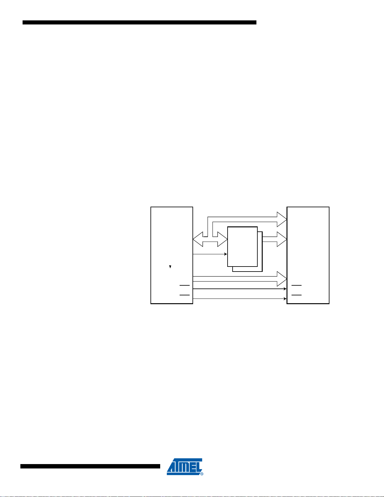
4.5 External Memory Interface
With all the features the External Memory Interface provides, it is well suited to operate as an
interface to m em ory devi ces s uch as Exte rnal SR AM a nd F lash , a nd p eriph eral s su ch as L CDdisplay, A/D, and D/A. The main features are:
• Four different wait-state settings (including no wait-state).
• Independent wait-state setting for different extErnal Memory sectors (configurable sector
size).
• The number of bits dedicated to address high byte is selectable.
• Bus keepers on data lines to minimize current consumption (optional).
4.5.1 Overview
When the eXternal MEMory (XME M) is enabl ed, address space outs ide the in ternal SRA M
becomes available us in g th e d edi ca ted Ex ter na l M emo ry p ins (s ee Fi gu re 1- 2 o n p age 5 or Fig-
ure 1-3 on page 6, Table 9-3 on page 74, Table 9-9 on page 78, and Table 9-21 on page 88).
The memory configuration is shown in Figure 4-4.
7679F–CAN–11/07
27
AT90CAN32/64/128
Figure 4-4. External Memory with Sector Select
Internal memory
0x0000
ISRAM end
XMem start
Lower sector
SRW01
SRW00
SRL[2..0]
4.5.2 Using the External Memory Interface
The interface consists of:
• AD7:0: Multiplexed low-order address bus and data bus.
• A15:8: High-order address bus (configurable number of bits).
• ALE: Address latch enable.
•RD
: Read strobe.
: Write strobe.
•WR
The control bits for the External Memory Interface are located in two registers, the External
Memory Control Register A – XMCRA, and the External Memory Control Register B – XMCRB.
When the XMEM interface is enabled, the XMEM interface will override the setting in the data
direction registers that correspon ds to the ports dedic ated to the XMEM in terface. Fo r details
about the port override, see the alternate functions in section “I/O-Ports” on page 66. The XMEM
interface will aut o-dete ct whet her an acce ss is intern al or exte rnal. If the acces s is e xternal , the
XMEM interface will o utput address , data, an d the con trol s ignals o n the p orts acc ording to Fig-
ure 4-6 (this figure shows the wave forms without wait-states). When ALE goes from high-to-low,
there is a valid addr ess on AD7:0. A LE is lo w durin g a data tr ansf er. Wh en the XM EM int erfac e
is enabled, also an internal access will cause activity on address, data and ALE ports, but the
and WR strobes will not toggl e during in terna l acce ss. Wh en the Exter nal Mem ory Inter face
RD
is disabled, the normal pin and data direction settings are used. Note that when the XMEM interface is disabled, the address space above the internal SRAM boundary is not mapped into the
internal SRAM. Figure 4-5 illustrate s how to co nnect an ex terna l SRA M to the AVR u sing an
octal latch (typically “74x573” or equivalent) which is transparent when G is high.
External Memory
(0-64K x 8)
Upper sector
SRW11
SRW10
0xFFFF
28
7679F–CAN–11/07
4.5.3 Address Latch Requirements
Due to the high-speed operation of the XRAM interface, the address latch must be selected with
care for system frequencies above 8 MHz @ 4V and 4 MHz @ 2.7V. When operating at conditions above these frequencies, the typical old style 74HC series latch becomes inadequate. The
External Memory Interface is desi gned in com plianc e to the 74A HC seri es latch. H owever , mos t
latches can be used as long they comply with the main timing parameters. The main parameters
for the address latch are:
AT90CAN32/64/128
• D to Q propagation delay (t
• Data setup time before G low (t
• Data (address) hold time after G low (
PD
).
).
SU
).
TH
The External Memory Interface is designed to guaranty minimum address hold time after G is
asserted low of t
tion 26.9 on page 375. The D-to-Q propagation delay (t
= 5 ns. Refer to t
h
LAXX_LD
/ t
LLAXX_ST
in Table 26-7 through Table 26- 14 of Sec-
) must be taken into consideration
PD
when calculating the access time requirement of the external component. The data setup time
before G low (t
) must not exceed address va lid to AL E low (t
SU
) minus PCB wiring delay
AVLLC
(dependent on the capacitive load).
Figure 4-5. External SRAM Connected to the AVR
D[7:0]
AD7:0
AVR
A15:8
ALE
RD
WR
DQ
G
A[7:0]
SRAM
A[15:8]
RD
WR
4.5.4 Pull-up and Bus-keeper
The pull-ups on the A D7:0 po rt s may b e ac tiv ate d i f t he co rres po ndi ng Po rt regi s ter i s wr itte n to
one. To reduce power consum pti on in sleep mo de, it is recommended to disabl e the pul l-up s by
writing the Port register to zero before entering sleep.
The XMEM interface also provides a bus-keeper on the AD7:0 lines. The bus-keeper can be disabled and enabled in softwar e as d escribed i n “Ex tern al Memo ry Co ntrol Regi ster B – XMC RB”
on page 33. When enabled, the bus-keeper will ensure a defined logic level (zero or one) on the
AD7:0 bus when these lines would otherwise be tri-stated by the XMEM interface.
4.5.5 Timing
External Memory devices have different timing requirements. To meet these requirements, the
AT90CAN32/64/128 XMEM interface provides four different wait-states as shown in Table 4-4. It
is important to co nsider the timin g speci ficat ion of the Ex ternal M emory d evice before se lectin g
the wait-state. The most important parameters are the access time for the external memory
compared to the set-up requirement of the AT90CAN32/64/128. The access time for the External Memory is defin ed t o be the time from rece iv in g th e c hip se le ct/address until the data of this
7679F–CAN–11/07
29
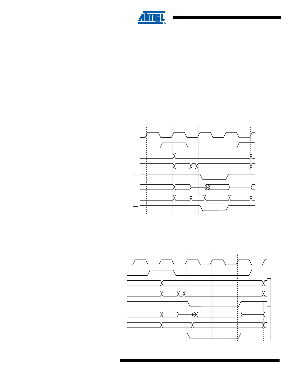
AT90CAN32/64/128
address actual ly is d riven on the bus. The acces s tim e canno t exce ed the t ime from the ALE
pulse must be asserted lo w until data is stab le during a read sequence (se e t
LLRL
+ t
RLRH
- t
DVRH
in Table 26-7 th ro ugh Tabl e 26 - 14). T he di fferent wait-states are se t up in so ftwar e. As an add itional feature, it is possible to divide the exter nal memory space in two sectors with individua l
wait-state settings. This makes it possible to connect two different memory devices with different
timing requirem ents to the same XMEM interface . For XMEM i nterface ti ming deta ils, pleas e
refer to Table 26-7 through Table 2 6-14 and Figur e 26-6 to Figure 26-9 in the “External Data
Memory Characteristics” on page 375.
Note that the XMEM interface is asynchronous and that the waveforms in the following figures
are related to the internal system clock. The skew between the internal and external clock
(XTAL1) is not guarantied (varies betw een device s temperature, and sup ply voltage) . Consequently, the XMEM interface is not suited for synchronous operation.
Figure 4-6. External Data Memory Cycles no Wait-state (SRWn1=0 and SRWn0=0)
System Clock (CLK
DA7:0 (XMBK = 0)
DA7:0 (XMBK = 1)
CPU
ALE
A15:8
DA7:0
WR
RD
T1 T2 T3
)
AddressPrev. addr.
Address DataPrev. data XX
DataPrev. data Address
XXXXX XXXXXXXX
DataPrev. data Address
T4
(1)
Write
Read
Note: 1. SRWn1 = SRW11 (upper sector) or SRW01 (lower sector), SRWn0 = SRW10 (upper secto r) or
SRW00 (lower sector). The ALE pulse in period T4 is only present if the next instruction
accesses the RAM (internal or external).
Figure 4-7. External Data Memory Cycles with SRWn1 = 0 and SRWn0 = 1
System Clock (CLK
CPU
T1 T2 T3
)
T4
(1)
T5
30
ALE
A15:8
DA7:0
WR
DA7:0 (XMBK = 0)
DA7:0 (XMBK = 1)
RD
Address DataPrev. data XX
AddressPrev. addr.
Write
DataPrev. data Address
DataPrev. data Address
7679F–CAN–11/07
Read
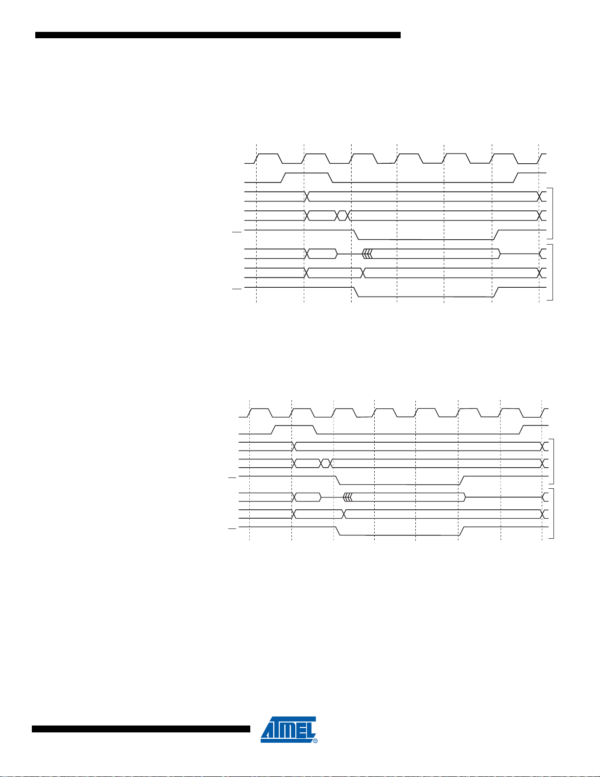
AT90CAN32/64/128
Note: 1. SRWn1 = SRW11 (upper sector) or SRW01 (lower sector), SRWn0 = SRW10 (upper secto r) or
SRW00 (lower sector).
The ALE pulse in period T5 is only present if the next instruction accesses the RAM (internal
or external).
Figure 4-8. External Data Memory Cycles with SRWn1 = 1 and SRWn0 = 0
System Clock (CLK
DA7:0 (XMBK = 0)
DA7:0 (XMBK = 1)
CPU
ALE
A15:8
DA7:0
WR
RD
T1 T2 T3
)
AddressPrev. addr.
Address DataPrev. data XX
DataPrev. data Address
DataPrev. data Address
T4 T5
(1)
T6
Note: 1. SRWn1 = SRW11 (upper sector) or SRW01 (lower sector), SRWn0 = SRW10 (upper secto r) or
SRW00 (lower sector).
The ALE pulse in period T6 is only present if the next instruction accesses the RAM (internal
or external).
Figure 4-9. External Data Memory Cycles with SRWn1 = 1 and SRWn0 = 1
System Clock (CLK
CPU
)
T1 T2 T3
ALE
T4 T5 T6
(1)
T7
Write
Read
A15:8
DA7:0
WR
DA7:0 (XMBK = 0)
DA7:0 (XMBK = 1)
RD
Address DataPrev. data XX
AddressPrev. addr.
DataPrev. data Address
DataPrev. data Address
Note: 1. SRWn1 = SRW11 (upper sector) or SRW01 (lower sector), SRWn0 = SRW10 (upper secto r) or
SRW00 (lower sector).
The ALE pulse in period T7 is only present if the next instruction accesses the RAM (internal
or external).
Write
Read
7679F–CAN–11/07
31

AT90CAN32/64/128
4.5.6 External Memory Control Register A – XMCRA
Bit 76543210
SRE SRL2 SRL1 SRL0 SRW11 SRW10 SRW01 SRW00 XMCRA
Read/Write R/W R/W R/W R/W R/W R/W R/W R/W
Initial Value00000000
• Bit 7 – SRE: External SRAM/XMEM Enable
Writing SRE to one enables the External Memory Interface.The pin functions AD7:0, A15:8,
ALE, WR
, and RD are activated as the alterna te pin functions. T he SRE bit overrides any pi n
direction setti ngs in the re spective dat a directi on register s. Writing S RE to zero, di sables th e
External Memory Interface and the normal pin and data direc tion settings are used. Note that
when the XMEM interf ace is di sabl ed, the ad dress s pace a bove th e intern al SR AM bou ndary is
not mapped into the internal SRAM.
• Bit 6..4 – SRL2, SRL1, SRL0: Wait-state Sector Limit
It is possible to configure different wait-states for different External Memory addresses. The
external memory address space can be divided in two sectors that have separate wait-state bits.
The SRL2, SRL1, and SRL0 bits select the split of the sectors, see Table 4-3 and Figure 4-4. By
default, the SRL2, SRL1, and SRL 0 bits ar e set to zero and the enti re ex ternal memo r y add ress
space is treated as one sector. When the entire SRAM address space is configured as one sector, the wait-states are configured by the SRW11 and SRW10 bits.
Table 4-3. Sector limits with different settings of SRL2..0
SRL2 SRL1 SRL0 Sector Addressing
Lower sector N/A
000
Upper sector “XMem start”
Lower sector “XMem start”
(1)
- 0xFFFF
(1)
- 0x1FFF
001
Upper secto r 0x2000 - 0xFFFF
Lower sector “XMem start”
(1)
- 0x3FFF
010
Upper secto r 0x4000 - 0xFFFF
Lower sector “XMem start”
(1)
- 0x5FFF
011
Upper secto r 0x6000 - 0xFFFF
Lower sector “XMem start”
(1)
- 0x7FFF
100
Upper secto r 0x8000 - 0xFFFF
Lower sector “XMem start”
(1)
- 0x9FFF
101
Upper sector 0xA000 - 0xFFFF
Lower sector “XMem start”
(1)
- 0xBFFF
110
Upper sector 0xC000 - 0xFFFF
Lower sector “XMem start”
(1)
- 0xDFFF
111
Upper sector 0xE000 - 0xFFFF
Note: 1. See Table 4-1 on page 18 for “XMemstart” setting.
32
7679F–CAN–11/07

AT90CAN32/64/128
• Bit 3..2 – SRW11, SRW10: Wait-state Select Bits for Upper Sector
The SRW11 and SRW10 bits control the number of wait-states for the upper sector of the external memory address space, see Table 4-4.
• Bit 1..0 – SRW01, SRW00: Wait-state Select Bits for Lower Sector
The SRW01 and SRW00 bi ts co ntr ol the number of wait-states fo r the l owe r se cto r of th e ex te rnal memory address space, see Table 4-4.
Table 4-4. Wait States
SRWn1 SRWn0 W ait S tates
0 0 No wait-states
0 1 Wait one cycle d uring read/w rite strobe
1 0 Wait two cycles during read/write strobe
11
Note: 1. n = 0 or 1 (lower/upper sector).
For further details of the timing and wait-states of the External Memory Interface, see Figures
4-6 through Figures 4-9 for how the setting of the SRW bits affects the timing.
(1)
Wait two cycles during read/write and wait one cycle before driving out new
address
4.5.7 External Memory Control Register B – XMCRB
Bit 76543210
XMBK––––XMM2XMM1XMM0XMCRB
Read/WriteR/WRRRRR/WR/WR/W
Initial Value00000000
• Bit 7– XMBK: External Memory Bus-keeper Enable
Writing XMBK to one enables the bus keeper on the AD7:0 lines. When the bus keeper is
enabled, it will ensure a defined logic level (zero or one) on AD7:0 when they would otherwise
be tri-stated. Writing XMBK to zero disables the bus keeper. XMBK is not qualified with SRE, so
even if the XMEM interface is disabled, the bus keepers are still activated as long as XMBK is
one.
7679F–CAN–11/07
• Bit 6..4 – Reserved Bits
These are reserved bits and will always read as zero. When writing to this address location,
write these bits to zero for compatibility with future devices.
• Bit 2..0 – XMM2, XMM1, XMM0: External Memory High Mask
When the External Memory is enabled, all Port C pins are default used for the high address byte.
If the full address space is not required to access the External Memory, some, or all, Port C pins
can be releas ed for no rmal Port Pi n funct ion as de scrib ed in Table 4-5. As described in “Using
all 64KB Locat ions of E xternal M emory” on page 3 5, it is possibl e to use the XMMn bits to
access all 64KB locations of the External Memory.
33

AT90CAN32/64/128
Table 4-5. Port C Pins Released as Normal Port Pins when the External Memory is Enabled
XMM2 XMM1 XMM0 # Bits for External Memory Address Released Port Pins
0 0 0 8 (Full External Memory Space) None
0017 PC7
0 1 0 6 PC7 .. PC6
0 1 1 5 PC7 .. PC5
1 0 0 4 PC7 .. PC4
1 0 1 3 PC7 .. PC3
1 1 0 2 PC7 .. PC2
1 1 1 No Address high bits Full Port C
4.5.8 Using all Locations of External Memory Smaller than 64 KB
Since the external memory is mapped after the internal memory as shown in Figure 4-4, the
external memory is not addressed when addressing the first “ISRAM size” bytes of data space. It
may appear that the first “ISRAM size” bytes of the external memory are inaccessible (external
memory addresses 0x0000 to “ISRAM end”). Howev er, when connecting an external memory
smaller than 64 KB , fo r ex amp le 32 K B, the se lo ca tio ns are easily accessed si mpl y by ad dres sing from address 0x8000 to “ISRAM end + 0x8000”. Since the External Memory Address bit A15
is not connected to th e external memor y, addresses 0x 8000 to “ISRAM e nd + 0x8000” will
appear as addresses 0x0000 to “ISRAM end” for the external memory. Addressing above
address “ISRAM end + 0x8000” is not recommended, since this will address an external memory location that is already accessed by another (lower) address. To the Application software,
the external 32 KB memory will appear as one linear 32 KB address space from “XMem start” to
“XMem start + 0x8000”. This is illustrated in Figure 4-10.
Figure 4-10. Address Map with 32 KB External Memory
AVR Memory Map
0x0000
Internal Memory
ISRAM end
XMem start
External Memory
0x7FFF
0x8000
ISRAM end + 0x8000
XMem start + 0x8000
(Unused)
0xFFFF
External 32K SRAM (Size=0x8000)
0x0000
ISRAM end
XMem start
0x7FFF
34
7679F–CAN–11/07

4.5.9 Using all 64KB Locations of External Memory
Since the External Memory is mapped after the Internal Memory as shown in Figure 4-4, only
(64K-(“ISRAM size”+256)) bytes of External Memo ry is available by default (address space
0x0000 to “ISRAM end ” is r eserv ed for interna l mem ory). However , it is po ssib le to take a dvantage of the entire External Memory by masking the higher address bits to zero. This can be done
by using the XMMn bits and contro l by softwa re the most sign ifica nt bits of the addre ss. By s etting Port C to output 0x00, and r eleasing th e most s ignifi cant bit s for normal Port Pin operatio n,
the Memory Interface will address 0x0000 - 0x1FFF. See the following code examples.
AT90CAN32/64/128
Assembly Code Example
; OFFSET is defined to 0x2000 to ensure
; external memory access
; Configure Port C (address high byte) to
; output 0x00 when the pins are released
; for normal Port Pin operation
ldi r16, 0xFF
out DDRC, r16
ldi r16, 0x00
out PORTC, r16
; release PC7:5
ldi r16, (1<<XMM1)|(1<<XMM0)
sts XMCRB, r16
; write 0xAA to address 0x0001 of external
; memory
ldi r16, 0xaa
sts 0x0001+OFFSET, r16
; re-enable PC7:5 for external memory
ldi r16, (0<<XMM1)|(0<<XMM0)
sts XMCRB, r16
; store 0x55 to address (OFFSET + 1) of
; external memory
ldi r16, 0x55
sts 0x0001+OFFSET, r16
C Code Example
(1)
(1)
7679F–CAN–11/07
#define OFFSET 0x2000
void XRAM_example(void)
{
unsigned char *p = (unsigned char *) (OFFSET + 1);
DDRC = 0xFF;
PORTC = 0x00;
XMCRB = (1<<XMM1) | (1<<XMM0);
*p = 0xaa;
XMCRB = 0x00;
*p = 0x55;
}
Note: 1. The example code assumes that the part specific header file is included.
Care must be exercised using this option as most of the memory is masked away.
35

AT90CAN32/64/128
4.6 General Purpose I/O Registers
The AT90CAN32/64/12 8 c ont ain s three Ge neral P ur pose I/O Registers. These re g ister s c an b e
used for storing any inform ation, and they are par ticu larly us eful for storing global variab les an d
status flags.
The General Purpose I/O Register 0, within the address range 0x00 - 0x1F, is directly bit-accessible using the SBI, CBI, SBIS, and SBIC instructions.
4.6.1 General Purpose I/O Register 0 – GPIOR0
Bit 76543210
GPIOR07 GPIOR06 GPIOR05 GPIOR04 GPIOR03 GPIOR02 GPIOR01 GPIOR00 GPIOR0
Read/Write R/W R/W R/W R/W R/W R/W R/W R/W
Initial Value00000000
4.6.2 General Purpose I/O Register 1 – GPIOR1
Bit 76543210
GPIOR17 GPIOR16 GPIOR15 GPIOR14 GPIOR13 GPIOR12 GPIOR11 GPIOR10 GPIOR1
Read/Write R/W R/W R/W R/W R/W R/W R/W R/W
Initial Value00000000
4.6.3 General Purpose I/O Register 2 – GPIOR2
Bit 76543210
GPIOR27 GPIOR26 GPIOR25 GPIOR24 GPIOR23 GPIOR22 GPIOR21 GPIOR20 GPIOR2
Read/Write R/W R/W R/W R/W R/W R/W R/W R/W
Initial Value00000000
36
7679F–CAN–11/07

5. System Clock
5.1 Clock Systems and their Distribution
Figure 5- 1 presents the principal clock systems in the AVR and their distribution. All of the clocks
need not be active at a given time . In order to re duce power consu mption, the clocks to unuse d
modules can be halted by using different sleep modes, as described in “Power Management and
Sleep Modes” on page 46. The clock systems are detailed below.
Figure 5-1. Clock Distribution
AT90CAN32/64/128
CLKO
Timer/Counter2
Asynchronous
Timer/Counter2
CKOUT Fuse
External Clock
Multiplexer
CAN
Controller
Timer/Counter2
Oscillator
TOSC2
General I/O
Modules
clk
clk
ASY
External Clock
ADC
clk
ADC
I/O
AVR Clock
Control Unit
Prescaler
Clock
Multiplexer
CPU Core RAM
clk
CPU
clk
FLASH
Reset Logic
Source clock
Crystal
Oscillator
XTAL2TOSC1 XTAL1
Watchdog Timer
Watchdog clock
Low-frequency
Crystal Oscillator
Watchdog
Oscillator
Flash and
EEPROM
Calibrated RC
Oscillator
5.1.1 CPU Clock – clk
The CPU clock is routed to parts of the system concerned with operation of the AVR core.
Examples of such module s are the General Purpo se Regis ter File , the Stat us Regi ster an d the
data memory holding the Stack Poin ter. Ha lti ng the CP U c lo ck i nhi bits the core from perfo r min g
general operations and calculations.
5.1.2 I/O Clock – clk
I/O
The I/O clock is used by the majority of the I/O modules, like Timer/Counters, SPI, CAN,
USART. The I/O clock is also used by the External Interrupt module, but note that some external
interrupts are detected by asynchronous logic, allowing such interrupts to be detected even if the
I/O clock is halted. Also note that address recognition in the TWI module is carried out asynchronously when clk
5.1.3 Flash Clock – clk
The Flash clock controls operation of the Flash interface. The Flash clock is usually active simultaneously with the CPU clock.
7679F–CAN–11/07
CPU
FLASH
is halted, enabling TWI address reception in all sleep modes.
I/O
37

AT90CAN32/64/128
5.1.4 Asynchronous Timer Clock – clk
The Asynchronous Timer clock allows the Asynchronous Timer/Counter to be clocked directly
from an external clock or an external 32 kHz clock crystal. The dedicated clock domain allows
using this Timer/Counter as a real-time counter even when the device is in sleep mode.
ASY
5.1.5 ADC Clock – clk
5.2 Clock Sources
ADC
The ADC is provided with a dedicate d cl oc k dom ain. T his allows hal tin g the CP U and I/O cloc ks
in order to reduce noise generated by digital circuitry. This gives more accurate ADC conversion
results.
The device has the f ollowing clock source opti ons, selectab le by Flash Fuse bits as shown
below. The clock from the selected source is input to the AVR clock generator, and routed to the
appropriate modules.
Table 5-1. Device Clocking Options Select
Device Clocking Option CKSEL3..0
E xternal Crystal/Ceramic Resonator 1111 - 1000
External Low-frequency Cr ystal 01 11 - 0100
Calibrated Internal RC Oscillator 0010
External Clock 0000
Reserved 0011, 0001
Note: 1. For all fuses “1” means unprogrammed while “0” means programmed.
(1)
The various choices for each clocking option is given in the following sections. When the CPU
wakes up from Powe r-down or Power-sa ve, the se lected clo ck sourc e is used to ti me the star tup, ensuring stable Oscillator operation before instruction execution starts. When the CPU starts
from reset, there is an add iti ona l de lay al lo win g the p o wer to r ea ch a sta bl e le ve l be for e s tarting
normal operation. The Watchdog Oscillator is used for timing this real-time part of the start-up
time. The number of WDT Oscillator cycles used for each time-out is shown in Table 5-2. The
frequency of the Watchdog Oscill ator is voltage depende nt as shown in “AT90CAN32/ 64/12 8
Typical Characteristics” on page 384.
Table 5-2. Number of Watchdog Oscillator Cycles
5.3 Default Clock Source
The device is shipped with CKSEL = “0010”, SUT = “10”, and CKDIV8 programmed. The default
clock source setti ng is the Intern al RC O scill ator w ith lon gest star t-up ti me and an ini tial s ystem
clock prescaling of 8. This def ault setting ensur es that all users can make their desired clock
source setting using an In-System or Parall el pr ogram mer .
38
Typ Time-out (VCC = 5.0V) Typ Time-out (VCC = 3.0V) Number of Cycles
4.1 ms 4.3 ms 4K (4,096)
65 ms 69 ms 64K (65,536)
7679F–CAN–11/07

5.4 Crystal Oscillator
XTAL1 and XTAL2 are input and output, respectively, of an inverting amplifier which can be configured for use as an On-chip Oscillator, as shown in Figure 5-2. Either a quartz crystal or a
ceramic resonator may be used.
C1 and C2 should always be equal for both c rystals and reso nators. The optim al value of the
capacitors depends o n the crystal or resona tor i n u se , the am oun t of str ay c ap ac itan ce , an d th e
electromagneti c noise of the environme nt. Some in itial guid elines for choosing capacitors for
use with crystals are given in Table 5-3. For ceramic resonators, the capacitor values given by
the manufacturer shoul d be used. For more in formati on on how to choose capacitors and other
details on Oscillator operation, refer to the Multi-purpose Oscillator Application Note.
Figure 5-2. Crystal Oscillator Connections
AT90CAN32/64/128
C2
C1
XTAL2
XTAL1
GND
The Oscillator can operate in three different modes, each optimized for a specific frequency
range. The operating mode is selected by the fuses CKSEL3..1 as shown in Table 5-3.
Table 5-3. Crystal Oscillator Operating Modes
CKSEL3..1 Frequency Range (MHz)
(1)
100
101 0.9 - 3.0 12 - 22
110 3.0 - 8.0 12 - 22
111 8.0 - 16.0 12 - 22
Note: 1. This option should not be used with crystals, only with ceramic resonators.
0.4 - 0.9 12 - 22
Recommended Range for Capacitors C1 and
C2 for Use with Crystals (pF)
7679F–CAN–11/07
The CKSEL0 Fuse toge the r with th e S UT 1..0 Fu ses select the start-up tim es as s ho wn in Table
5-4.
39

AT90CAN32/64/128
Table 5-4. Start-up Times for the Oscillator Clock Selection
Start-up Time from
CKSEL0 SUT1..0
0 00 258 CK
0 01 258 CK
010 1K CK
011 1K CK
100 1K CK
1 01 16K CK 14 CK
1 10 16K CK 14 CK + 4.1 ms
1 11 16K CK 14 CK + 65 ms
Notes: 1. These options should only be used when not operating cl ose to the maximu m freque ncy of the
device, and only if frequency stability at start-up is not important for the application. These
options are not suitable for crystals.
2. These options are intend ed fo r use with cerami c reson ators a nd will en sure freq ue ncy st abi lity
at start-up. They can also be used with crystals when not operating close to the maximum frequency of the device, and if frequency stability at start-up is not important for the application.
Power-down and
Power-save
(1)
(1)
(2)
(2)
(2)
Additional Delay
from Reset
= 5.0V)
(V
CC
14 CK + 4.1 ms
14 CK + 65 ms
14 CK
14 CK + 4.1 ms
14 CK + 65 ms
Recommended Usage
Ceramic resonator, fast
rising power
Ceramic resonator , slo wly
rising power
Ceramic resonator, BOD
enabled
Ceramic resonator, fast
rising power
Ceramic resonator , slo wly
rising power
Crystal Oscillator, BOD
enabled
Crystal Oscillator, fast
rising power
Crystal Oscillator, slowly
rising power
5.5 Low-frequency Crystal Oscillator
To use a 32.768 kHz watch cr ystal a s the cl ock sou rce fo r the devi ce, the l ow-frequ ency cr ystal
Oscillator must be s elected by setting the CKSEL Fuses to “ 0100”, “010 1”, “0110”, or “0111” .
The crystal should be connected as shown in Figure 5-3.
Figure 5-3. Low-frequency Crystal Oscillator Connections
12-22 pF capacitors may be necessary if the parasitic impedance (pads, wires & PCB) is very
low.
12 - 22 pF
XTAL2
32.768 KHz
XTAL1
12 - 22 pF
GND
40
7679F–CAN–11/07

AT90CAN32/64/128
When this Oscillator is selected, start-up times are determined by the SUT1..0 fuses as shown in
Table 5-5 and CKSEL1..0 fuses as shown in Table 5-6.
Table 5-5. Start-up Times for the Low-frequency Crystal Oscillator Clock Selection
SUT1..0 Additional Delay from Reset (VCC = 5.0V) Recommended Usage
00 14 CK Fast rising power or BOD enabled
01 14 CK + 4.1 ms Slowly rising power
10 14 CK + 65 ms Stable frequency at start-up
11 Reserved
Table 5-6. Start-up Times for the Low-frequency Crystal Oscillator Clock Selection
CKSEL3..0
(1)
0100
0101 32K CK Stable frequency at start-up
(1)
0110
0111 32K CK Stable frequency at start-up
Note: 1. These options should only be used if frequency stability at start-up is not important for the
application
5.6 Calibrated Internal RC Oscillator
The calibrated internal RC Oscillator provides a fixed 8.0 MHz clock. The frequency is nominal
value at 3V and 25°C. If 8 MHz frequency exc eeds th e spec ificati on of the devic e (depen ds on
), the CKDIV8 Fuse m ust be prog ramme d in ord er to divide the in ternal frequen cy by 8 du r-
V
CC
ing start-up. The device is shipped with the CKDIV8 Fuse programmed. See “System Clock
Prescaler” on page 44. for mo re detai ls . This cl oc k ma y be sel ect ed as t he sys tem clo ck by pr o-
gramming the CKSEL Fuses as shown in Table 5-7. If selected, it will operate with no external
components. During reset, hardware loads the calibration byte into the OSCCAL Register and
thereby automatically calibrates the RC Oscillator. At 5V and 25°C, this calibration gives a frequency within ± 10% of the nominal frequency. Using calibration methods as described in
application notes available at www.a tmel .com/ avr it is possib le to ach ieve ± 2% accuracy at any
given V
lator will still be used for the Watchdog T imer and for the Reset Time -out. For more informa tion
on the pre-programmed calibration value, see the section “Calibration Byte” on page 339.
CC and temperature. When this Os cill ator is used as the ch ip clock, t he Watc hdog O sci l-
Start-up Time from
Power-down and Power-save
1K CK
1K CK
Recommended Usage
7679F–CAN–11/07
Table 5-7. Internal Calibrated RC Oscillator Operating Modes
CKSEL3..0 Nominal Frequency
0010 8.0 MHz
Note: 1. The device is shipped with this option selected.
(1)
41

AT90CAN32/64/128
When this Oscillator is selected, start-up times are determined by the SUT Fuses as shown in
Table 5-8.
Table 5-8. Start-up times for the internal calibrated RC Oscillator clock selection
SUT1..0
00 6 CK 14 CK BOD enabled
01 6 CK 14 CK + 4.1 ms Fast rising power
(1)
10
11 Reserved
Note: 1. The device is shipped with this option selected.
Start-up Time from Power-
down and Power-save
6 CK 14 CK + 65 ms Slowly rising power
5.6.1 Oscillator Calibration Register – OSCCAL
Bit 76543210
– CAL6 CAL5 CAL4 CAL3 CAL2 CAL1 CAL0 OSCCAL
Read/Write R R/W R/W R/W R/W R/W R/W R/W
Initial Value 0 <----- ------- --- - Device Specific Calibration Valu e ----------- ----->
• Bit 7 – Reserved Bit
This bit is reserved for future use.
• Bits 6..0 – CAL6..0: Oscillator Calibration Value
Writing the calibration byte to this address will trim the internal Oscillator to remove process variations from the Oscillator frequency. This is done automatically during Chip Reset. When
OSCCAL is zero, the lowest available frequency is chosen. Writing non-zero values to this register will increase the fr equency o f the intern al Oscillator . Writing 0x 7F to the register gives the
highest available frequency. The calibrated Oscillator is used to time EEPROM and Flash
access. If EEPROM or Flash is written, do not calibrate to more than 10% above the nominal frequency. Otherwise , th e E EPR OM o r F lash write may fail. Note that th e Os ci ll ato r is i nten ded for
calibration to 8.0 MHz. Tuning to other values is not guaranteed, as indicated in Table 5-9.
Additional Delay from
Reset (V
= 5.0V)
CC
Recommended Usage
5.7 External Clock
42
Table 5-9. Internal RC Oscillator Frequency Range.
OSCCAL Value
0x00 50% 100%
0x3F 75% 150%
0x7F 100% 200%
Min Frequency in Percentage of
Nominal Frequency
Max Frequency in Percentage of
Nominal Frequency
To drive the devic e from an extern al clock source , XTAL 1 should be drive n as show n in Figure
5-4. To run the device on an external clock, the CKSEL Fuses must be programmed to “0000”.
7679F–CAN–11/07

Figure 5-4. External Clock Drive Configuration
AT90CAN32/64/128
NC
XTAL2
External
Clock
XTAL1
Signal
GND
Table 5-10. Ex te rn al Clock Freque nc y
CKSEL3..0 Frequency Range
0000 0 - 16 MHz
When this clock source is selected, start-up times are determined by the SUT Fuses as shown in
Table 5-11.
Table 5-11. Start-up Times for the External Clock Selection
SUT1..0
00 6 CK 14 CK BOD enabled
01 6 CK 14 CK + 4.1 ms Fast rising power
Start-up Time from Power-
down and Power-save
Additional Delay from
Reset (V
= 5.0V)
CC
Recommended Usage
10 6 CK 14 CK + 65 ms Slowly rising power
11 Reserved
When applying an external clock, it is required to avoid sudden changes in the applied clock frequency to ensure stable operation of the MCU. A variation in frequency of more than 2% from
one clock cycle to the next can lead to unpredictable behavior. It is required to ensure that the
MCU is kept in Reset during such changes in the clock frequency.
Note that th e Syst em Cl oc k Pres cale r can be us ed t o impl eme nt ru n-t ime chan ges of th e int ern al
clock frequency while still ensuring stable operation. Refer to “System Clock Prescaler” on page
44 for details.
5.8 Clock Output Buffer
When the CKOUT Fuse is programmed, the system Clock will be output on CLKO. This mode is
suitable when chip clock is used to drive other circuits on the system. The clock will be output
also during reset and the n ormal o peration o f I/O pi n will be overridde n when th e fuse i s programmed. Any clock source, including internal RC Oscillator, can be selected when CLKO
serves as clock outpu t. If t he S y ste m Cl ock P r es ca ler i s used, i t i s t he d iv ided s y ste m clo ck th at
is output (CKOUT Fuse programmed).
5.9 Timer/Counter2 Oscilla tor
For AVR microcon trol lers with Ti mer /Counte r2 Os cilla tor pin s (T OSC1 a nd T OSC2) , the crys tal
is connected dire ctly betwee n the pins. The Osc illator is op timized for use wi th a 32.768 kHz
watch crystal. 12-22 pF capacitors may be necessary if the parasitic impedance (pads, wires &
PCB) is very low.
7679F–CAN–11/07
43

AT90CAN32/64/128
AT90CAN32/64/128 share the Timer/Counter2 Oscillator Pins (TOSC1 and TOSC2) with PG4
and PG3. This means that both PG4 and PG3 can only be used when the Timer/Counter2 Oscillator is not enable.
Applying an external clock source to TOSC1 can be done in asynchronous operation if EXTCLK
in the ASSR Register is written to logic one. See “Asynchronous operation of the
Timer/Counter2” on page 160 for further description on selecting external clock as input instead
of a 32 kHz crystal. In this configuration, PG4 cannot be used but PG3 is available.
5.10 System Clock Prescaler
The AT90CAN32/64/12 8 system clock can be divi ded by setting t he Cloc k Pres cale r Regist er –
CLKPR. This feature can be used to decrease power consumption when the requirement for
processing power is low. This can be used with all clock source options, and it will affect the
clock frequenc y of the CPU and a ll synchr onous periph eral s. clk
are divided by a factor as shown in Table 5-12.
5.10.1 Clock Prescaler Register – CLKPR
Bit 76543210
CLKPCE – – – CLKPS3 CLKPS2 CLKPS1 CLKPS0 CLKPR
Read/Write R/W R R R R/W R/W R/W R/W
Initial Value 0 0 0 0 <----- See Bit Description ----->
• Bit 7 – CLKPCE: Clock Prescaler Change Enable
The CLKPCE bit must be written to logic one to enable change of the CLKPS bits. The CLKPCE
bit is only updated when th e oth er bits i n CLKPR a re si mul tan eou sl y wri tten t o ze ro . CLK PCE is
cleared by hardware four cycle s after it is writt en or wh en CLKP S bit s are writte n. Rewrit ing the
CLKPCE bit within this tim e-out period does neither extend the time-out period , nor clear the
CLKPCE bit.
I/O
, clk
ADC
, clk
CPU
, and clk
FLASH
44
• Bit 6..0 – Reserved Bits
These bits are reserved for future use.
• Bits 3..0 – CLKPS3..0: Clock Prescaler Select Bits 3 - 0
These bits define the division factor between the selected clock source and the internal system
clock. These bit s can be writt en run-time to vary the clock freque ncy to sui t the applic ation
requirements. As the divider divides the master clock input to the MCU, the speed of all synchronous peripherals is reduced when a division factor is used. The division factors are given in
Table 5-12.
To avoid unintentional changes of clock frequency, a special write procedure must be followed
to change the CLKPS bits:
1. Write the Clock Prescaler Change Enable (CLKPCE) bit to one and all other bits in
CLKPR to zero.
2. Within four cycles, write the desired value to CLKPS while writing a zero to CLKPCE.
Interrupts must be disabled when changing prescaler setting to make sure the write procedure is
not interrupted.
The CKDIV8 Fuse de termine s the initi al value of th e CLKPS bits. If C KDIV8 is un progra mmed,
the CLKPS bits wil l be reset to “0000” . If CKDIV8 is pro grammed, CLKP S bits are reset to
7679F–CAN–11/07

AT90CAN32/64/128
“0011”, giving a division factor of 8 at start up. This feature shou ld be used if the sele cted clock
source has a higher frequency than the maximum frequency of the device at the present operating conditions. Note that any value can be written to the CLKPS bits regardless of the CKDIV8
Fuse setting. The Application software must ensure that a sufficient division factor is chosen if
the selected cloc k s ource h as a highe r frequ ency than t he max imum freq uency o f the d evic e at
the present operating conditions. The device is shipped with the CKDIV8 Fuse programmed.
Table 5-12. Clock Prescaler Select
CLKPS3 CLKPS2 CLKPS1 CLKPS0 Clock Division Factor
00001
00012
00104
00118
010016
010132
011064
0111128
1000256
1 0 0 1 Reserved
1 0 1 0 Reserved
1 0 1 1 Reserved
1 1 0 0 Reserved
1 1 0 1 Reserved
1 1 1 0 Reserved
1 1 1 1 Reserved
Note: The frequency of the asynchronous clock must be lower than 1/4th of the frequency of the scaled
down Source clock. Otherwise, interrupts may be lost, and accessing the Timer/Counter2 registers may fail.
7679F–CAN–11/07
45

AT90CAN32/64/128
6. Power Management and Sleep Modes
Sleep modes enable the application to shut down unused modules in the MCU, thereby saving
power. The AVR provides various sleep modes allowing the user to tailor the power consumption to the application’s requirements.
To enter any of the five sleep modes, th e SE bit in SMCR m ust be written to lo gic one and a
SLEEP instruction must be executed. The SM2, SM1, and SM0 bits in the SMCR Register select
which sleep mode (Idle, ADC Noise Reduction, Power-down, Power-save, or Standby) will be
activated by the SLEEP instruction. See Table 6-1 for a summary. If an enabled interrupt occurs
while the MCU is in a sleep mode, the MCU wakes up. The MCU is then halted for four cycles in
addition to the start-up time, executes the interrupt routine, and resumes execution from the
instruction following SLEEP . The conte nts of the registe r file and SRAM are unal tered when the
device wakes up fro m sleep. If a reset oc curs duri ng sleep m ode, th e MCU wakes u p and executes from the Reset Vector.
Figure 5-1 on page 37 presents the different clock systems in the AT90CAN32/64/128, and their
distribution. The figure is helpful in selecting an appropriate sleep mode.
6.0.1 Sleep Mode Control Register – SMCR
The Sleep Mode Control Register contains control bits for power management.
Bit 76543210
– – – – SM2 SM1 SM0 SE SMCR
Read/Write R R R R R/W R/W R/W R/W
Initial Value00000000
• Bit 7..4 – Reserved Bits
These bits are reserved for future use.
• Bits 3..1 – SM2..0: Sleep Mode Select Bits 2, 1, and 0
These bits select between the five available sleep modes as shown in Table 6-1.
Table 6-1. Sleep Mode Select
SM2 SM1 SM0 Sleep Mode
000Idle
0 0 1 ADC Noise Reduction
0 1 0 Power-down
0 1 1 Power-save
1 0 0 Reserved
1 0 1 Reserved
1 1 0 Standby
1 1 1 Reserved
Note: 1. Standby mode is only recommended for use with external crystals or resonators.
(1)
• Bit 1 – SE: Sleep Enable
The SE bit must be written to logic one to make the MCU enter the sleep mode when the SLEEP
instruction is executed. To avoid the MCU entering the sleep mode unless it is the programmer’s
46
7679F–CAN–11/07

purpose, it is recommended to write the Sleep Enable (SE) bit to one just before the execution of
the SLEEP instruction and to clear it immediately after waking up.
6.1 Idle Mode
When the SM2 ..0 bits are written t o 000, the SLEEP in struction makes the MCU enter Idle
mode, stopping the CPU but allowing SPI, CAN, USART, Analog Comparator, ADC, Two-wire
Serial Interface, Timer/Counters, Watchdog, and the interrupt system to continue operating. This
sleep mode basically halts clk
Idle mode enables the MCU to wake up from external triggered interrupts as well as internal
ones like the Timer Overflow and USART Transmit Complete interrupts. If wake-up from the
Analog Comparator interrupt is not required, the Analog Comparator can be powered down by
setting the ACD bit in the Analog Comparator Control and Status Register – ACSR. This will
reduce power consumption in Idle mode. If the ADC is enabled, a conversion starts automatically when this mode is entered.
6.2 ADC Noise Reduction Mode
When the SM2..0 bits are written to 001, the SLEEP instruction makes the MCU enter ADC
Noise Reduction mode, stopping the CPU but allowing the ADC, the External Interrupts, the
Two-wire Serial Interface address watch, Timer/Counter2, CAN and the Watchdog to continue
operating (if enabled) . Thi s s lee p mo de ba si ca ll y ha lts cl k
the other clocks to run.
CPU
and clk
AT90CAN32/64/128
, while allowing the other clocks to run.
FLASH
I/O
, clk
CPU
, and clk
, while allowing
FLASH
This improves the noi se envi ronment fo r the ADC, enablin g higher re solution measurem ents. If
the ADC is enabled, a conversion starts automatically when this mode is entered. Apart from the
ADC Conversion Complete interrupt, only an External Reset, a Watchdog Reset, a Brown-out
Reset, a Two-wire Serial Interface address match interrupt, a Timer/ Counter2 interru pt, an
SPM/EEPROM ready interrupt, an External Level Interrupt on INT7:4, or an External Interrupt on
INT3:0 can wake up the MCU from ADC Noise Reduction mode.
6.3 Power-down Mode
When the SM2..0 bits are written to 010, the SLEEP instruction makes the MCU enter Powerdown mode. In this mode, the External Oscillator is stopped, while the External Interrupts, the
Two-wire Serial Interface address watch, and the Watchdog continue operating (if enabled).
Only an External Reset, a Watchdog Reset, a Brown-out Reset, a Two-wire Serial Interface
address match int errupt, an Exte rnal Level Inter rupt on INT7:4, o r an External Inte rrupt on
INT3:0 can wake up the MCU . This sleep mod e basicall y halts all gener ated clocks , allowing
operation of asynchronous modules only.
Note that if a level triggered in terrupt is used for wake- up from Po wer-down mode, the cha nged
level must be held for some tim e to wak e up the MC U. R efer to “External Interrupts” on page 93
for details.
When waking up from Power-down mode, there is a del ay from the wake-up c ondition occurs
until the wake-up becomes effective. This all ows the clock to resta rt and beco me st able after
having been stopp ed. The wake -up period is defined by the same CK SEL fuse s that define th e
Reset Time-out period, as described in “Clock Sources” on page 38.
6.4 Power-save Mode
When the SM2..0 bits are written to 011, the SLEEP instruction makes the MCU enter Powersave mode. This mode is identical to Power-down, with one exception:
7679F–CAN–11/07
47

AT90CAN32/64/128
If Timer/Counter2 is clocked asynchronously, i.e., the AS2 bit in ASSR is set, Timer/Counter2
will run during sleep. The device can wake up from either Timer Overflow or Output Compare
event from Timer/Counter2 if the corresponding Timer/Counter2 interrupt enable bits are set in
TIMSK2, and the global interrupt enable bit in SREG is set.
If the Asynchronous Timer is NOT clocked asynchronously, Power-down mode is recommended
instead of Power-save mode becaus e the contents o f the registers in the async hronous timer
should be considered undefined after wake-up in Power-save mode if AS2 is 0.
This sleep mode basic ally halts all cl ocks except clk
, allowing operation only of asynchronous
ASY
modules, including Timer/Counter2 if clocked asynchronously.
6.5 Standby Mode
When the SM2..0 bits are 110 and an External Crystal/Resonator clock option is selected, the
SLEEP instruc tion make s th e MCU enter Sta ndby mode. Thi s m ode i s iden tica l to Power -do wn
with the excepti on tha t th e Osc illat or i s k ept r unning. From Standby m ode , th e dev ice wak es u p
in 6 clock cycles.
Table 6-2. Active Clock Domains and Wake-up Sources in the Different Sleep Modes.
Active Clock Domains Oscillators Wake-up Sources
Sleep
Mode
clk
CPU
clk
FLASH
clkIOclk
ADC
clk
ASY
Main
Clock
Source
Enabled
Idle X X X X X
ADC Noise
Reduction
XX X X
Powerdown
Powersave
Standby
(1)
(2)
X
XX
Notes: 1. Only recommended with external crystal or resonator selected as clock source.
2. If AS2 bit in ASSR is set.
3. Only INT3:0 or level interrupt INT7:4.
Timer
Osc.
Enabled
(2)
(2)
(2)
X
INT7:0
TWI
Address
Match
XXXXXX
(3)
X
(3)
X
(3)
X
(3)
XX
X
XX
X
Timer
2
(2)
(2)
SPM/
EEPROM
Ready
ADC
XX
Other
I/O
6.6 Minimizing Power Consumption
There are several issues to c ons id er when tr yi ng to min imiz e the pow er con sumpti on i n an AV R
controlled system. In gener al, slee p modes shou ld be u sed as much as poss ible , and the sleep
mode should be selected so that as few as possible of the device’s functions are operating. All
functions not needed sho uld be disa bled. In part icular, the following modul es may nee d specia l
consideration when trying to achieve the lowest possible power consumption.
6.6.1 Analog to Digital Converter
If enabled, the ADC will be enable d in a ll s leep mode s. T o save power, the A DC shou ld be disabled before entering any sleep mode. When the ADC is turned off and on again, the next
conversion will be an extended conversion. Refer to “Analog to Digital Converter - ADC” on page
273 for details on ADC operation.
48
7679F–CAN–11/07

6.6.2 Analog Comparator
When entering Idle mode, the Analog Comparator should be disabled if not used. When entering
ADC Noise Reduction mod e, th e A nal og Co mpa rator s hou ld b e di sabl ed. I n oth er sl ee p mo des ,
the Analog Comparator is automatically disabled. However, if the Analog Comparator is set up
to use the Internal Volta ge Re fer ence a s i nput , the A na log Comp arator should be disabled i n al l
sleep modes. Otherwise, the Internal Voltage Reference will be enabled, independent of sleep
mode. Refer to “ Analog Co mparator ” on page 269 fo r details on how to conf igure the Ana log
Comparator.
6.6.3 Brown-out Detector
If the Brown-out Detector is not needed by the application, this module should be turned off. If
the Brown-out Detector is enabled by the BODLEVEL Fuses, it will be enabled in all sleep
modes, and hence, alway s cons ume power. In th e dee per sl eep m odes, this wi ll con tribu te si gnificantly to the total c ur rent co nsu mpt ion . Refe r to “ Brown -out Detection” on page 54 for d etails
on how to configure the Brown-out Detector.
6.6.4 Internal Voltage Reference
The Internal Voltage Reference will be enabled when needed by the Brown-out Detection, the
Analog Comparator or the ADC. If these modules are disabled as describ ed in the sections
above, the internal vol tage refer ence will be dis abled and i t will no t be consum ing powe r. Whe n
turned on again, the user must allow the reference to start up before the output is used. If the
reference is kept on in sleep m ode, the output c an be used im mediat ely. Ref er to “In terna l Volt-
age Reference” on page 56 for details on the start-up time.
AT90CAN32/64/128
6.6.5 Watchdog Timer
If the Watchdog Timer is not needed in the application, the module should be turned off. If the
Watchdog Timer is enabled, it will be enabled in all sleep modes, and hence, always consume
power. In the deeper sle ep mode s, this will contribu te signif icant ly to th e total c urrent c onsu mption. Refer to “Watchdog Timer” on page 57 for details on how to configure the Watchdog Timer.
6.6.6 Port Pins
When entering a sleep mode, all port pins should be configured to use minimum power. The
most important is then to ensure that no pins drive resistive loads. In sleep modes where both
the I/O clock (clk
) and the ADC clock (clk
I/O
be disabled. This ensure s that no power is con sumed by the input logic when not nee ded. In
some cases, the input logic is needed for detecting wake-up conditions, and it will then be
enabled. Refer to th e section “ Digital Inp ut Enabl e and Sleep Mo des” on pa ge 70 for detai ls on
which pins are enabled. If the input buffer is enab led and the input signal is left floati ng or have
an analog signal level close to V
For analog input pins, the digital input buffer should be disabled at all times. An analog signal
level close to V
/2 on an input pin can c ause sig nificant curren t even in acti ve mode. Di gital
CC
input buffers can be disabled by writing to the Digital Input Disable Registers (DIDR1 and
DIDR0). Refer to “Digital Input Di sable Register 1 – DIDR 1” on pag e 272 an d “Di gital Input Dis-
able Register 0 – DIDR0” on page 292 for details.
6.6.7 JTAG Interface and On-chip Debug System
If the On-chip debug system is enabled by OCDEN Fuse and the chip enter sleep mode, the
main clock source is en abl ed, and h enc e, a lwa ys cons um es powe r. I n the dee per s lee p mo des ,
) are stopped, th e inp ut bu ffers of the dev ice wi ll
ADC
/2, the input buffer will use excessive power.
CC
7679F–CAN–11/07
49

AT90CAN32/64/128
this will contribute significantly to the total current consumption. There are three alternative ways
to avoid this:
• Disable OCDEN Fuse.
• Disable JTAGEN Fuse.
• Write one to the JTD bit in MCUCR.
The TDO pin is left floating when the JTAG interface is enabled while the JTAG TAP controller is
not shifting data. If the hardware connected to the TDO pin does not pull up the logic level,
power consumption will increase. Note that the TDI pin for the next device in the scan chain contains a pull-up that avoids this problem. Writing the JTD bit in the MCUCR register to one or
leaving the JTAG fuse unprogrammed disables the JTAG interface.
50
7679F–CAN–11/07

7. System Control and Reset
7.1 Reset
7.1.1 Resetting the AVR
During reset, a ll I/O Re gister s are s et to th eir in itial va lues, a nd the p rogram s tarts executio n
from the Reset Vector. The instruction placed at the Reset Vector must be a JMP – Absolute
Jump – instruction to the reset handling routine. If the program never enables an interrupt
source, the Interr upt Vecto rs are not us ed, and regular pr ogram cod e can be placed at t hese
locations. This is also the case if the Reset Vector is in the Application section while the Interrupt
Vectors are in the Boot sec tion or vice versa. The circ uit diagram i n Figure 7-1 shows the reset
logic. Table 7-1 defines the electrical parameters of the reset circuitry.
The I/O ports of the AVR a re immedia tely reset to their initial state when a reset sour ce goes
active. This does not require any clock source to be running.
After all reset sources have gone inactive, a delay counter is invoked, stretching the internal
reset. This allows the power to re ach a s tabl e l evel b efor e n or mal ope ra tio n s tarts . The ti me- o ut
period of the delay counter i s defined by the user th rough th e SUT and C KSEL Fuse s. The different selections for the delay period are presented in “Clock Sources” on page 38.
AT90CAN32/64/128
7.1.2 Reset Sources
The AT90CAN32/64/128 has five sources of reset:
• Power-on Reset. The MCU is reset when the supply voltage is below the Power-on Reset
threshold (V
• External Reset. The MCU is reset when a low level is present on the RESET
than the minimum pulse length.
• Watchdog Reset. The MCU is reset when the Watchdog Timer period expires and the
Watchdog is enabled.
• Brown-out Reset. The MCU is reset when the supply voltage V
Reset threshold (V
• JTAG AVR Reset. The MCU is reset as long as there is a logic one in the Reset Register, one
of the scan chains of the JTAG system. Refer to the section “Boundary-scan IEEE 1149.1
(JTAG)” on page 300 for details.
POT
).
) and the Brown-out Detector is enabled.
BOT
pin for longer
is below the Brown-out
CC
7679F–CAN–11/07
51

AT90CAN32/64/128
Figure 7-1. Reset Logic
BODLEVEL [2..0]
Pull-up Resistor
Spike
Filter
JTAG Reset
Register
Power-on Reset
Circuit
Brown-out
Reset Circuit
Watchdog
Oscillator
DATA BUS
MCU Status
Register (MCUSR)
JTRF
BORF
PORF
WDRF
EXTRF
Clock
Generator
CKSEL[3:0]
SUT[1:0]
CK
Delay Counters
TIMEOUT
Table 7-1. Reset Characteristics
Symbol Parameter Condition Min. Typ. Max. Units
Power-on Reset Threshold Voltage (rising) 1.4 2.3 V
V
V
V
CCRR
V
t
POT
POR
RST
RST
Power-on Reset Threshold Voltage (falling)
Vcc Start Voltage to ensure
internal Power-on Reset signal
Vcc Rise Rate to ensure
internal Power-on Reset signal
RESET Pin Threshold Voltage
Minimum pulse width on RESET Pin Vcc = 5 V, temperature = 25 °C 400 ns
Note: 1. The Power-on Reset will not work unless the supply voltage has been below V
(1)
1.3 2.3 V
- 0.05 GND + 0.05 V
0.3 V/ms
POT
0.2
Vcc
(falling)
0.85
Vcc
7.1.3 Power-on Reset
A Power-on Reset (POR) pulse is generated by an On-chip detection circuit. The detection level
is defined in Table 7-1. The POR is activated whenever V
is below the detection le vel. The
CC
POR circuit can be used to trigger the start-up Reset, as well as to detect a failure in supply
voltage.
V
A Power-on Reset (POR) circuit ensures that the device is properly reset from Power-on if V
started from V
voltage invokes the delay counter, which determines how long the device is kept in RESET after
52
with a rise rate upper than V
POR
. Reaching the Power-on Reset threshol d
CCRR
7679F–CAN–11/07
CC

AT90CAN32/64/128
VCC rise. The RESET signal is activated again, without any delay, when VCC decreases below
the detection level.
Figure 7-2. MCU Start-up, RESET
V
CCRR
V
CC
RESET
TIME-OUT
INTERNAL
RESET
V
POR
Tied to V
V
POT
t
TOUT
V
CCRR
CC
Figure 7-3. MCU Start-up, RESET Extended Externally
V
CCRR
V
CC
RESET
V
POR
V
RST
7.1.4 External Reset
TIME-OUT
INTERNAL
RESET
Note: If V
POR
or V
parameter range can not be followed, an External Reset is required.
CCRR
An External Reset is ge nerated by a low level on the RESET
t
TOUT
pin. Reset pulses longer than the
minimum pulse width (see Table 7-1) will generate a reset, even i f the clock is not running.
Shorter pulse s are not gu arante ed to gene rate a reset . When the applie d signal rea ches the
Reset Threshold Voltage – V
the Time-out period – t
TOUT –
– on its positive edge, the delay counter starts the MCU after
RST
has expired.
7679F–CAN–11/07
53

AT90CAN32/64/128
Figure 7-4. External Reset During Operation
7.1.5 Brown-out Detection
AT90CAN32/64/128 has an On-chip Brown-out Detection (BOD) circuit for monitoring the V
level during operation by comparing it to a fixed trigger level. The trigger level for the BOD can
be selected by the BODLE VEL Fuses. The trig ger level has a hysteres is to ensu re spike fr ee
Brown-out Detection. The hysteresis on the detection level should be interpreted as V
V
BOT
Table 7-2. BODLEVEL Fuse Coding
+ V
HYST
CC
/2 and V
BOT-
= V
BOT
- V
HYST
/2.
(1)
BOT+
CC
=
BODLEVEL 2..0 Fuses Min V
BOT
Typ V
BOT
Max V
BOT
Units
111 BOD Disabled
110 4.1 V
101 4.0 V
100 3.9 V
011 3.8 V
010 2.7 V
001 2.6 V
000 2.5 V
Note: 1. V
may be below nominal minimum operating voltage for some devices. For devices where
BOT
this is the case, the device is tested down to V
antees that a Brown-Out Reset will occur before V
= V
CC
during the production test. This guar-
BOT
drops to a voltage where correct
CC
operation of the microcontroller is no lon ger gua ranteed. The test is performed using
BODLEVEL = 010 for Low Operating Voltage and BODLEVEL = 101 for High Operating Voltage .
Table 7-3. Brown-out Characteristics
Symbol Parameter Min. Typ. Max. Units
V
t
BOD
HYST
Brown-out Detector Hysteresis 70 mV
Min Pulse Width on Brown-out Reset 2 µs
When the BOD is enabled, and VCC decreases to a value below the trigger level (V
7-5), the Brown-ou t R es et i s im mediately activate d. W he n V
54
in Figure
BOT-
increases abov e th e t rigge r le ve l
CC
7679F–CAN–11/07

AT90CAN32/64/128
(V
in Figure 7-5), the delay counter s tarts the MCU afte r the Time-out period t
BOT+
expired.
TOUT
has
7.1.6 Watchdog Reset
The BOD circuit will only detect a drop in V
longer than t
given in Table 7-1.
BOD
if the voltage stays below the trigger level for
CC
Figure 7-5. Brown-out Reset During Operation
V
CC
RESET
TIME-OUT
INTERNAL
RESET
V
BOT-
V
BOT+
t
TOUT
When the Watchdog times out, i t will gen erate a short r eset pul se of one CK cycle duration . On
the falling edge of this pul se, the delay timer starts co unting the Time-out pe riod t
TOUT
. Refer to
page 57 for details on operation of the Watchdog Timer.
Figure 7-6. Watchdog Reset During Operation
CC
7.1.7 MCU Status Register – MCUSR
The MCU Status Register provides information on which reset source caused an MCU reset.
Bit 76543210
Read/Write R R R R/W R/W R/W R/W R/W
Initial Value 0 0 0 See Bit Description
CK
– – – JTRF WDRF BORF EXTRF PORF MCUSR
7679F–CAN–11/07
• Bit 7..5 – Reserved Bits
These bits are reserved for future use.
55

AT90CAN32/64/128
• Bit 4 – JTRF: JTAG Reset Flag
This bit is set if a reset is being caused by a logic one in the JTAG Reset Register selected by
the JTAG instruction AVR_RESET. This bit is reset by a Power-on Reset, or by writing a logic
zero to the flag.
• Bit 3 – WDRF: Watchdog Reset Flag
This bit is set if a W atchdog Re se t occurs. The bit i s reset by a P ower-on Reset, or by wr iting a
logic zero to the flag.
• Bit 2 – BORF: Brown-out Reset Flag
This bit is set if a Brown-out Reset occurs. The bit is reset by a Power-on Reset, or by writing a
logic zero to the flag.
• Bit 1 – EXTRF: External Reset Flag
This bit is set if an Exte rnal Rese t occurs. Th e bit is rese t by a Powe r-on Res et, or by writi ng a
logic zero to the flag.
• Bit 0 – PORF: Power-on Reset Flag
This bit is set if a Power-on Reset occurs. The bit is reset only by writing a logic zero to the flag.
To make use of the Reset flags to identify a reset condition, the user should read and then reset
the MCUSR as early as possible in the program. If the register is cleared before another reset
occurs, the source of the reset can be found by examining the reset flags.
7.2 Internal Voltage Reference
AT90CAN32/64/128 features an internal bandgap reference. This reference is used for Brownout Detection, and it can be used as an input to the Analog Comparator or the ADC.
7.2.1 Voltage Reference Enable Signals and Start-up Time
The voltage reference has a start-up time that may influence the way it should be used. The
start-up time is given in Table 7-4. To save power, the reference is not always turned on. The
reference is on during the following situations:
1. When the BOD is enabled (by programming the BODLEVEL [2..0] Fuse).
2. When the bandgap reference is connected to the Analog Comparator (by setting the
ACBG bit in ACSR).
3. When the ADC is enabled.
Thus, when the BOD is not enabled, after setting the ACBG bit or enabling the ADC, the user
must always allow the reference to sta rt up before the output from the Ana log Comparator or
ADC is used. To reduce po wer co ns ump tio n in Power-down mode, the u se r can avo id the th re e
conditions above to ensure that the reference is turned off before entering Power-down mode.
56
7679F–CAN–11/07

7.2.2 Voltage Reference Characteristics
Table 7-4. Internal Voltage Reference Characteristics
Symbol Parameter Condition Min. Typ. Max. Units
AT90CAN32/64/128
7.3 Watchdog Timer
The Watchdog Timer is clocked from a separate On-chip Oscillator which runs at 1 MHz. This is
the typical value at V
controlling the Watchdog Timer prescaler , the Watchdog Reset interval can be adjuste d as
shown in Table 7-6 on page 58. The WDR – Watchdog Reset – instruction resets the Watchdog
Timer. The Watchd og Timer is al so reset wh en it is disabl ed and when a Chip Reset occ urs.
Eight different clock cycle periods can be selected to determine the reset period. If the reset
period expires without another Watchdog Reset, the AT90CAN32/64/128 resets and executes
from the Reset Vector. For timing details on the Watchdog Reset, refer to Table 7-6 on page 58.
To prevent unintentional disabling of the Watchdog or unintentional change of time-out period,
two different safety levels are selected by the fuse WDTON as shown in Table 7-5. Refer to
“Timed Sequen ces for Chang ing the Configu ration of the Watc hdog Timer” on page 59 for
details.
Table 7-5. WDT Configuration as a Function of the Fuse Settings of WDTON
V
BG
t
BG
I
BG
WDTON
Unprogrammed 1 Disabled Timed sequence Timed sequence
Bandgap reference voltage 1.0 1.1 1.2 V
Bandgap reference start-up time 40 70 µs
Bandgap reference current
consumption
= 5V. See characterization data for typical values at other VCC levels. By
CC
Safety
Level
WDT Initial
State
How to Disable
the WDT
15 µA
How to Change
Time-out
Programmed 2 Enabled Always enabled Timed sequence
Figure 7-7. Watchdog Timer
7.3.1 Watchdo g Timer Control Register – WDTCR
Bit 76543210
7679F–CAN–11/07
WATCHDOG
OSCILLATOR
~1 MHz
57

AT90CAN32/64/128
– – – WDCE WDE WDP2 WDP1 WDP0 WDTCR
Read/Write R R R R/W R/W R/W R/W R/W
Initial Value00000000
• Bits 7..5 – Reserved Bits
These bits are reserved bits for future use.
• Bit 4 – WDCE: Watchdog Change Enable
This bit must be set when the WDE b it is writ ten to log ic zero. Oth erwis e, the W atchdog wil l not
be disabled. Once written to on e, hardwar e will clear thi s bit after fo ur clock cy cles. Refe r to the
description of the WDE bit for a Watchdog d isable proc edure. This bit must also be set when
changing the prescaler bits. See “Timed Sequences for Changing the Configuration of the
Watchdog Timer” on page 59.
• Bit 3 – WDE: Watchdog Enab le
When the WDE is written to logic one, the Watchdog Timer is enabled, and if the WDE is written
to logic zero, the Watchdog Timer function is disabled. WDE can only be cleared if the WDCE bit
has logic level one. To disable an e nabled Watc hdog Timer , the following p rocedure mus t be
followed:
1. In the same operation, write a logic one to WDCE and WDE. A logic one must be written to WDE even though it is set to one before the disable operation starts.
2. Within the next four clock cycles, write a logic 0 to WDE. This disables the Watchdog.
In safety level 2, it is not possible to disable the Watchdog Timer, even with the algorithm
described a bove. See “Timed Sequences for Changing the Configuration of the Watchdog
Timer” on page 59.
• Bits 2..0 – WDP2, WDP1, WDP0: Watchdog Time r Prescaler 2, 1, and 0
The WDP2, WDP1, and W DP0 bits determine the Wa tch dog T im er pr escaling when the Watchdog Timer is enab led. The differe nt presca ling va lues and their co rrespo nding T imeout P eriods
are shown in Table 7-6.
Table 7-6. Watchdog Timer Prescale Select
WDP2 WDP1 WDP0
0 0 0 16K cycles 17.1 ms 16.3 ms
0 0 1 32K cycles 34.3 ms 32.5 ms
0 1 0 64K cycles 68.5 ms 65 ms
0 1 1 32/64K cycles 0.14 s 0.13 s
1 0 0 256K cycles 0.27 s 0.26 s
1 0 1 512K cycles 0.55 s 0.52 s
1 1 0 1,024K cycles 1.1 s 1.0 s
1 1 1 2,048K cycles 2.2 s 2.1 s
Number of WDT
Oscillator Cycles
Ty pical T ime-out at
= 3.0V
V
CC
T ypical T ime-out a t
VCC = 5.0V
58
7679F–CAN–11/07

AT90CAN32/64/128
The following code example shows one assembly and one C function for turning off the WDT.
The example assumes that interrupts are controlled (e.g. by disabling interrupts globally) so that
no interrupts will occur during execution of these functions.
Assembly Code Example
WDT_off:
; Write logical one to WDCE and WDE
ldi r16, (1<<WDCE)|(1<<WDE)
sts WDTCR, r16
; Turn off WDT
ldi r16, (0<<WDE)
sts WDTCR, r16
ret
C Code Example
void WDT_off(void)
{
/* Write logical one to WDCE and WDE */
WDTCR = (1<<WDCE) | (1<<WDE);
/* Turn off WDT */
WDTCR = 0x00;
}
(1)
(1)
Note: 1. The example code assumes that the part specific header file is included.
7.4 Timed Sequences for Changing the Configuration of the Watchdog Timer
The sequence for changing configuration differs slightly between the two safety levels. Separate
procedures are described for each level.
7.4.1 Safety Level 1
In this mode, the Watchdog Timer is initially disabled, but can be enabled by writing the WDE bit
to 1 without any restriction. A timed sequence is needed when changing the Watchdog Time-out
period or disabling an enabled Watchdog Timer. To disable an enabled Watchdog Timer, and/or
changing the Watchdog Time-out, the following procedure must be followed:
1. In the same operation, write a logic one to WDCE and WDE. A logic one must be written to WDE regardless of the previous value of the WDE bit.
2. Within the next four clock cycles, in the same operation, write the WDE and WDP bits
as desired, but with the WDCE bit cleared.
7.4.2 Safety Level 2
In this mode, the Watchdog Timer is always enabled, and the WDE bit will always read as one. A
timed sequence is needed when changing the Watchdog Time-out period. To change the
Watchdog Time-out, the following procedure must be followed:
1. In the same operation, write a logical one to WDCE and WDE. Even though the WDE
always is set, the WDE must be written to one to start the timed sequence.
2. Within the next four clock cycles, in the same operation, write the WDP bits as desired,
but with the WDCE bit cleared. The value written to the WDE bit is irrelevant.
7679F–CAN–11/07
59

AT90CAN32/64/128
8. Interrupts
This section describ es the specifics of the interrupt handling as performed in
AT90CAN32/64/128. For a gene ral explanation of the AV R interrupt handling, ref er to “Reset
and Interrupt Handling” on page 15.
8.1 Interrupt Vectors in AT90CAN32/64/128
Table 8-1. Reset and Interrupt Vectors
Vector
No.
10x0000
2 0x0002 INT0 External Interrupt Request 0
3 0x0004 INT1 External Interrupt Request 1
4 0x0006 INT2 External Interrupt Request 2
5 0x0008 INT3 External Interrupt Request 3
6 0x000A INT4 External Interrupt Request 4
7 0x000C INT5 External Interrupt Request 5
8 0x000E INT6 External Interrupt Request 6
9 0x0010 INT7 External Interrupt Request 7
10 0x0012 TIMER2 COMP Timer/Counter2 Compare Mat ch
1 1 0x0014 TIMER2 OVF Timer/Counter2 Ov erfl ow
12 0x0016 TIMER1 CAPT Timer/Counter1 Capture Event
13 0x0018 TIMER1 COMPA Timer/Counter1 Compare Match A
14 0x001A TIMER1 COMPB Timer/Counte r 1 Compare Match B
15 0x001C TIMER1 COMPC Timer/Counter1 Compare Mat ch C
Program
Address
Source Interrupt Definition
(1)
(2)
RESET
External Pin, Power-on Reset, Brown-out Reset,
Watchdog Reset, and JTAG AVR Reset
60
16 0x001E TIMER1 OVF Timer/Counte r1 Overflow
17 0x0020 TIMER0 COMP Timer/Counter0 Compare Mat ch
18 0x0022 TIMER0 OVF Timer/Counter0 Overfl ow
19 0x0024 CANIT CAN Transfer Complete or Error
20 0x0026 OVRIT CAN Tim er Overrun
21 0x0028 SPI, STC SPI Serial Transfer Complete
22 0x002A USART0, RX USART0, Rx Complete
23 0x002C USART0, UDRE USART0 Data Register Empty
24 0x002E USART0, TX USART0, Tx Complete
25 0x0030 ANALOG COMP Analog Comparator
26 0x0032 ADC ADC Conversion Complete
27 0x0034 EE READY EEPROM Ready
28 0x0036 TIMER3 CAPT Timer/Counter3 Capture Event
7679F–CAN–11/07

Table 8-1. Reset and Interrupt Vectors (Continued)
AT90CAN32/64/128
Vector
No.
29 0x0038 TIMER3 COMPA Timer/Counter3 Compare Match A
30 0x003A TIMER3 COMPB Timer/Counte r 3 Compare Match B
31 0x003C TIMER3 COMPC Timer/Counter3 Compare Mat ch C
32 0x003E TIMER3 OVF Timer/Counte r3 Overflow
33 0x0040 USART1, RX USART1, Rx Complete
34 0x0042 USART1, UDRE USART1 Data Register Empty
35 0x0044 USART1, TX USART1, Tx Complete
36 0x0046 TWI Two-wire Serial Interface
37 0x0048 SPM READY Store Program Memory Ready
Notes: 1. When the IVSEL bit in MCUCR is set, Interrupt Vectors will be moved to the start of the Boot
Program
Address
Flash Sect ion. The addr ess of each Interrupt Vector will then be the address in this table
added to the start address of the Boot Flash Section.
2. When the BOOTRST Fuse is pr ogramm ed, the de vice will ju mp to the Boot Loade r addr ess at
reset, see “Boot Loader Support – Read-While-Write Self-Programming” on page 321.
Source Interrupt Definition
(1)
Table 8-2 shows reset and Interrupt Vectors placement for the various combinations of
BOOTRST and IVSEL settings. If the program never enables an interrupt source, the Interrupt
Vectors are not used, and regular program code can be placed at these locations. This is also
the case if the Reset Vector is in the Application s ection while the Interrupt V ectors are in the
Boot section or vice versa.
Table 8-2. Reset and Interrupt Vectors Placement
BOOTRST IVSEL Reset Address Interrupt Vectors Start Address
1 0 0x0000 0x0002
1 1 0x0000 Boot Reset Address + 0x0002
0 0 Boot Reset Address 0x0002
0 1 Boot Reset Address Boot Reset Address + 0x0002
Note: 1. The Boot Reset Address is shown in Table 24-6 on page 334. For the BOOTRST Fuse “1”
means unprogrammed while “0” means programmed.
(1)
The most typical and general program setup for the Reset and Interrupt Vector Addresses in
AT90CAN32/64/128 is:
;Address Labels Code Comments
0x0000 jmp RESET ; Reset Handler
0x0002 jmp EXT_INT0 ; IRQ0 Handler
0x0004 jmp EXT_INT1 ; IRQ1 Handler
0x0006 jmp EXT_INT2 ; IRQ2 Handler
0x0008 jmp EXT_INT3 ; IRQ3 Handler
0x000A jmp EXT_INT4 ; IRQ4 Handler
0x000C jmp EXT_INT5 ; IRQ5 Handler
0x000E jmp EXT_INT6 ; IRQ6 Handler
0x0010 jmp EXT_INT7 ; IRQ7 Handler
7679F–CAN–11/07
61

AT90CAN32/64/128
0x0012 jmp TIM2_COMP ; Timer2 Compare Handler
0x0014 jmp TIM2_OVF ; Timer2 Overflow Handler
0x0016 jmp TIM1_CAPT ; Timer1 Capture Handler
0x0018 jmp TIM1_COMPA; Timer1 CompareA Handler
0x001A jmp TIM1_COMPB; Timer1 CompareB Handler
0x001C jmp TIM1_OVF ; Timer1 CompareC Handler
0x001E jmp TIM1_OVF ; Timer1 Overflow Handler
0x0020 jmp TIM0_COMP ; Timer0 Compare Handler
0x0022 jmp TIM0_OVF ; Timer0 Overflow Handler
0x0024 jmp CAN_IT ; CAN Handler
0x0026 jmp CTIM_OVF ; CAN Timer Overflow Handler
0x0028 jmp SPI_STC ; SPI Transfer Complete Handler
0x002A jmp USART0_RXC; USART0 RX Complete Handler
0x002C jmp USART0_DRE; USART0,UDR Empty Handler
0x002E jmp USART0_TXC; USART0 TX Complete Handler
0x0030 jmp ANA_COMP ; Analog Comparator Handler
0x0032 jmp ADC ; ADC Conversion Complete Handler
0x0034 jmp EE_RDY ; EEPROM Ready Handler
0x0036 jmp TIM3_CAPT ; Timer3 Capture Handler
0x0038 jmp TIM3_COMPA; Timer3 CompareA Handler
0x003A jmp TIM3_COMPB; Timer3 CompareB Handler
0x003C jmp TIM3_COMPC; Timer3 CompareC Handler
0x003E jmp TIM3_OVF ; Timer3 Overflow Handler
0x0040 jmp USART1_RXC; USART1 RX Complete Handler
0x0042 jmp USART1_DRE; USART1,UDR Empty Handler
0x0044 jmp USART1_TXC; USART1 TX Complete Handler
0x0046 jmp TWI ; TWI Interrupt Handler
0x0048 jmp SPM_RDY ; SPM Ready Handler
;
0x004A RESET: ldi r16, high(RAMEND) ; Main program start
0x004B out SPH,r16 ;Set Stack Pointer to top of RAM
0x004C ldi r16, low(RAMEND)
0x004D out SPL,r16
0x004E sei ; Enable interrupts
0x004F <instr> xxx
... ... ... ...
When the BOOTRST Fuse is unprogrammed, the Boot section size set to 8K bytes and the
IVSEL bit in the MCUCR Regis ter is set before a ny interru pts are enabl ed, the m ost typica l and
general program setup for the Reset and Interrupt Vector Addresses is:
62
;Address Labels Code Comments
0x0000 RESET: ldi r16,high(RAMEND) ; Main program start
0x0001 out SPH,r16 ; Set Stack Pointer to top of RAM
0x0002 ldi r16,low(RAMEND)
0x0003 out SPL,r16
7679F–CAN–11/07

AT90CAN32/64/128
0x0004 sei ; Enable interrupts
0x0005 <instr> xxx
;
.org (BootResetAdd + 0x0002)
0x..02 jmp EXT_INT0 ; IRQ0 Handler
0x..04 jmp PCINT0 ; PCINT0 Handler
... ... ... ;
0x..0C jmp SPM_RDY ; Store Program Memory Ready Handler
When the BOOTRST Fuse is programmed and the Boot section size set to 8K bytes, the most
typical and general program setup for the Reset and Interrupt Vector Addresses is:
;Address Labels Code Comments
.org 0x0002
0x0002 jmp EXT_INT0 ; IRQ0 Handler
0x0004 jmp PCINT0 ; PCINT0 Handler
... ... ... ;
0x002C jmp SPM_RDY ; Store Program Memory Ready Handler
;
.org (BootResetAdd)
0x..00 RESET: ldi r16,high(RAMEND) ; Main program start
0x..01 out SPH,r16 ; Set Stack Pointer to top of RAM
0x..02 ldi r16,low(RAMEND)
0x..03 out SPL,r16
0x..04 sei ; Enable interrupts
0x..05 <instr> xxx
7679F–CAN–11/07
When the BOOTRST Fuse is prog ra mme d, the Boot sect io n si ze set to 8K byte s an d the IV SE L
bit in the MCUCR Register is set before any interrupts are enabled, the most typical and general
program setup for the Reset and Interrupt Vector Addresses is:
;Address Labels Code Comments
;
.org (BootResetAdd)
0x..00 jmp RESET ; Reset handler
0x0002 jmp EXT_INT0 ; IRQ0 Handler
0x..04 jmp PCINT0 ; PCINT0 Handler
... ... ... ;
0x..44 jmp SPM_RDY ; Store Program Memory Ready Handler
;
0x..46 RESET: ldi r16,high(RAMEND) ; Main program start
0x..47 out SPH,r16 ; Set Stack Pointer to top of RAM
0x..48 ldi r16,low(RAMEND)
0x..49 out SPL,r16
0x..4A sei ; Enable interrupts
0x..4B <instr> xxx
63

AT90CAN32/64/128
8.2 Moving Interrupts Between Application and Boot Space
The General Interrupt Control Register controls the placement of the Interrupt Vector table.
8.2.1 MCU Control Register – MCUCR
Bit 76543210
JTD – – PUD – – IVSEL IVCE MCUCR
Read/Write R/W R R R/W R R R/W R/W
Initial Value00000000
• Bit 1 – IVSEL: Interrupt Vector Select
When the IVSEL bit is cleared (zero), the Interrupt Vectors are placed at the start of the Flash
memory. When this bit is set (one), the Interrupt Vectors are moved to the beginning of the Boot
Loader section of the Flash. The actual address of the start of the Boot Flash Section is determined by the BOOTSZ Fuses. Refer to the section
Programming” on page 321 for details. To avoid unintentional changes of Interrupt Vector tables, a
special write procedure must be followed to change the IVSEL bit:
1. Write the Interrupt Vector Change Enable (IVCE) bit to one.
2. Within four cycles, write the desired value to IVSEL while writing a zero to IVCE.
Interrupts will automa tic al ly be di sa bled while this sequence is exe cu ted. In ter r upts ar e di sa ble d
in the cycle IVCE is set, an d they remain disabled unti l aft er the i nstru ct ion f ollowi ng th e wr ite to
IVSEL. If IVSEL is not written, interrupts remain disabled for four cycles. The I-bit in the Status
Register is unaffected by the automatic disa bling.
“Boot Loader Support – Read-While-Write Self-
Note: If Interrupt Vectors are placed in the Boot Loader section and Boot Lock bit BLB02 is pro-
grammed, interrupt s are di sable d whil e executi ng from th e Applic ation section. If In terru pt Vectors
are placed in the Application section and Boot Lock bit BLB12 is programed, interrupts are disabled while executing from the Boot Loader section. Refer to the section “Boot Loader Support –
Read-While-Write Self-Programming” on page 321 for details on Boot Lock bits.
64
7679F–CAN–11/07

AT90CAN32/64/128
• Bit 0 – IVCE: Interrupt Vector Change Enable
The IVCE bit must be written to logic one to ena ble c hang e o f the IV SE L b it. IVC E i s cl ear e d by
hardware four cycles af ter i t i s writte n o r whe n IV S EL is wr itten . S etti ng the IV CE bi t will di s able
interrupts, as explained in the IVSEL description above. See Code Example below.
Assembly Code Example
Move_interrupts:
; Get MCUCR
in r16, MCUCR
mov r17, r16
; Enable change of Interrupt Vectors
ori r16, (1<<IVCE)
out MCUCR, r16
; Move interrupts to Boot Flash section
ori r17, (1<<IVSEL)
out MCUCR, r17
ret
C Code Example
void Move_interrupts(void)
{
uchar temp;
/* Get MCUCR*/
temp = MCUCR;
/* Enable change of Interrupt Vectors */
MCUCR = temp | (1<<IVCE);
/* Move interrupts to Boot Flash section */
MCUCR = temp | (1<<IVSEL);
}
7679F–CAN–11/07
65

AT90CAN32/64/128
9. I/O-Ports
9.1 Introduction
All AVR ports have true R ead-Modify -Write fu nctional ity when used as general digi tal I/O ports .
This means that the direction of one port pin can be changed without unintentionally changing
the direction of any other pin with th e SBI an d CBI i nstruc tions . The s ame app lies when cha nging drive value (if configured as output) or enabling/disabling of pull-up resistors (if configured as
input). Each output buffer has symmetrical drive characteristics with both high sink and source
capability. All port pins have individually selectable pull-up resistors with a supply-voltage invariant resistance. All I/O pins have protection diodes to both V
9-1. Refer to “Electrical Characteristics (1)” on page 365 for a complete list of parameters.
Figure 9-1. I/O Pin Equivalent Schematic
and Ground as indicated in Figure
CC
R
pu
Pxn
C
pin
"General Digital I/O" for
All registers and bit references in this section are written in general form. A lower case “x” represents the numbering letter for the port, and a lower case “n” represents the bit number. However,
when using the register or bit defines in a program, the precise form must be used. For example,
PORTB3 for bit no. 3 in Port B, here documented generally as PORTxn. The physical I/O Registers and bit locations are listed in “Register Description for I/O-Ports”.
Three I/O memory address locations are allocated for each port, one each for the Data Register
– PORTx, Data Directi on Regi ster – D DRx, and the Por t Input P ins – P INx. The Port Input Pins
I/O location is read only, while the Data Re gister and the Data Direc tio n Regi st er are rea d/writ e.
However, writing a logic one to a bit in the PINx Register, will result in a toggle in the corresponding bit in the Data Register. In addition, the Pull-up Disable – PUD bit in MCUCR disables the
pull-up function for all pins in all ports when set.
Using the I/O port as Gen eral D igital I/O is des c ribed in “ Po rts as G ene ral Di gi tal I/ O”. M o st port
pins are multiplexed with alternate functions for the peripheral features on the device. How each
alternate function interferes with the port pin is described in “Alternate P or t Fun cti ons” on page
71. Refer to the individual module sections for a full description of the alternate functions.
Logic
See Figure
Details
Note that enabling the alternate function of some of the port pins does not affect the use of the
other pins in the port as general digital I/O.
66
7679F–CAN–11/07

9.2 Ports as General Digital I/O
The ports are bi-directi onal I/O ports with optional inter nal pull-ups . Figure 9-2 show s a functional description of one I/O-port pin, here generically called Pxn.
AT90CAN32/64/128
Figure 9-2. General Digital I/O
Pxn
(1)
SLEEP
SYNCHRONIZER
DLQ
D
PINxn
Q
PUD
Q
D
DDxn
Q
CLR
RESET
Q
D
PORTxn
Q
CLR
RESET
Q
Q
RRx
WDx
RDx
RPx
clk
1
0
I/O
WPx
WRx
DATA BUS
Note: 1. WRx, WPx, WDx, RRx, RPx, and RDx are common to all pins within the same port. clk
9.2.1 Configuring the Pin
Each port pin con sis ts o f three regi ster bits: DDxn, P ORTx n, and PINx n. As shown in “Register
Description for I/O-Ports” on page 89, the DDxn bi ts are acces sed at the DDRx I/O address, the
PORTxn bits at the PORTx I/O address, and the PINxn bits at the PINx I/O address.
The DDxn bit in the DDRx Re gister selects th e direction of t his pin. If DDxn i s written logi c on e,
Pxn is configured as an output pin. If DDxn is written logic zero, Pxn is configured as an input
pin.
If PORTxn is writt en logi c one when the pin is c onfigur ed as an input pin, th e pull- up resi stor is
activated. To switch the pull-up resistor off, PORTxn has to be written logic zero or the pin has to
be configured as an output pin
The port pins are tri-stated when reset condition becomes active, even if no clocks are running.
PUD: PULLUP DISABLE
SLEEP: SLEEP CONTROL
clk
: I/O CLOCK
I/O
SLEEP, and PUD are common to all ports.
WDx: WRITE DDRx
RDx: READ DDRx
WRx: WRITE PORTx
RRx: READ PORTx REGISTER
RPx: READ PORTx PIN
WPx: WRITE PINx REGISTER
I/O
,
7679F–CAN–11/07
67

AT90CAN32/64/128
If PORTxn is writ ten lo gic one when the pin i s c onfi gu re d a s an output pin, the port pin is d ri ven
high (one). If PORTxn is wr itten logic zero when the pin is configured as an output pi n, the port
pin is driven low (zero).
9.2.2 Toggling the Pin
Writing a logic one to P INx n t oggl es the value of PORTx n, in dep end ent on the value of DDRxn.
Note that the SBI instruction can be used to toggle one single bit in a port.
9.2.3 Switching Between Input and Output
When switching bet ween tri-sta te ({DDxn, PORTxn} = 0b 00) and outpu t high ({DDx n, PORTxn}
= 0b11), an intermediate state with either pull- up enabled {DDxn, P ORTxn} = 0b01) or output
low ({DDxn, PORTxn} = 0b10) occurs. Normally, the pull-up enabled state is fully acceptable, as
a high-impedant environment will not notice the difference between a strong high driver and a
pull-up. If this is not the case, the PUD bit in the MCUC R Registe r can be set to disable al l pullups in all ports.
Switching between input with pull-up and output low generates the same problem. The user
must use either the tri-state ({DDxn, PORTxn} = 0b00) or the output high state ({DDxn, PORTxn}
= 0b11) as an intermediate step.
Table 9-1 summarizes the control signals for the pin value.
Table 9-1. Port Pin Configurations
DDxn PORTxn
0 0 X Input No
0 1 0 Input Yes Pxn will source current if ext. pulled low.
0 1 1 Inp ut No Tri-state (Hi-Z)
1 0 X Output No Output Low (Sink)
1 1 X Output No Output High (Source)
9.2.4 Reading the Pin Value
Independent of the setting of Data Direction bit DDxn, the port pin can be r ead through the
PINxn Register bit. As shown in Figure 9-2, the PINxn Register bit and the preceding latch c onstitute a synchr onizer. T his is needed to avoid metastabi lity if th e physi cal pin change s value
near the edge of the internal clock, but it also introduces a delay. Figure 9-3 shows a timing diagram of the synchronization when reading a n externally applied pin value. The maximum and
minimum propagation delays are denoted t
PUD
(in MCUCR)
I/O Pull-up Comment
Default configuration after Reset.
Tri-state (Hi-Z)
pd,max
and t
respectively.
pd,min
68
7679F–CAN–11/07

AT90CAN32/64/128
Figure 9-3. Synchronization when Reading an Externally Applied Pin value
SYSTEM CLK
INSTRUCTIONS
XXX in r17, PINx
XXX
SYNC LATCH
PINxn
r17
0x00 0xFF
t
pd, max
t
pd, min
Consider the clock period starting shortly after the first falling edge of the system clock. The latch
is closed when the clock is low, and goes transparent when the clock is high, as indicated by the
shaded region of the “S YNC LATCH” signal. The s ignal v alue is l atche d when t he syste m clock
goes low. It is clocked into the PINxn Register a t the succeeding pos itive clock edge. A s indicated by the two arr ows t
pd,max
and t
, a single signal transition on the pin will be delayed
pd,min
between ½ and 1½ system clock period depending upon the time of assertion.
When reading back a software assigned pin value, a nop in struction must be inserted as indi-
cated in Figure 9-4. The out instruction sets the “SYNC LATCH” signal at the positive edge of
the clock. In this case, the delay t
through the synchronizer is 1 system clock period.
pd
Figure 9-4. Synchronization when Reading a Software Assigned Pin Value
SYSTEM CLK
r16
INSTRUCTIONS
out PORTx, r16 nop in r17, PINx
0xFF
SYNC LATCH
PINxn
r17
0x00 0xFF
t
pd
7679F–CAN–11/07
69

AT90CAN32/64/128
The following code e xampl e s ho ws how to set port B pins 0 a nd 1 hi gh, 2 an d 3 lo w, an d de fin e
the port pins from 4 to 7 as input with pull-ups assigned to port pins 6 and 7. The resulting pin
values are read back again, but as previously discussed, a nop instruction is included to be able
to read back the value recently assigned to some of the pins.
Assembly Code Example
...
; Define pull-ups and set outputs high
; Define directions for port pins
ldi r16, (1<<PB7)|(1<<PB6)|(1<<PB1)|(1<<PB0)
ldi r17, (1<<DDB3)|(1<<DDB2)|(1<<DDB1)|(1<<DDB0)
out PORTB, r16
out DDRB, r17
; Insert nop for synchronization
nop
; Read port pins
in r16, PINB
...
C Code Example
unsigned char i;
...
/* Define pull-ups and set outputs high */
/* Define directions for port pins */
PORTB = (1<<PB7)|(1<<PB6)|(1<<PB1)|(1<<PB0);
DDRB = (1<<DDB3)|(1<<DDB2)|(1<<DDB1)|(1<<DDB0);
/* Insert nop for synchronization*/
_NOP();
/* Read port pins */
i = PINB;
...
(1)
(1)
Note: 1. For the assembly program, two temporary registers are used to minimize the time from pull-
9.2.5 Digital Input Enable and Sleep Modes
As shown in Figure 9-2, the digital input signal can be clamped to ground at the input of the
schmitt-trigger. The signal denoted SLEEP in the figure, is set by the MCU Sleep Controller in
Power-down mode, Power-save mode, and Standby mode to avoid high power consumption if
some input signals are left floating, or have an analog signal level close to V
SLEEP is overridden for port pins enabled as external interrupt pins. If the external interrupt
request is not enabled, SLEEP is active also for these pins. SLEEP is also overridden by various
other alternate functions as described in “Alternate Port Functions” on page 71.
If a logic high level (“one”) is present on an Asynchronous External Interrupt pin configured as
“Interrupt on Rising Edge, Falling Edge, or Any Logic Change on Pin” while the external interrupt
is not enabled, th e corresp onding Ex ternal Int errupt Fl ag will be se t when resu ming from th e
70
ups are set on pins 0, 1, 6, and 7, until the direction bits are correctly set, defining bit 2 and 3
as low and redefining bits 0 and 1 as strong high drivers.
/2.
CC
7679F–CAN–11/07

above mentioned sleep modes, as the clamping in these sleep modes produces the requested
logic change.
9.2.6 Unconnected Pins
If some pins are unused, it is recommended to ensure that these pins have a defined level. Even
though most of the digital inputs are disabled in the deep sleep modes as described above, floating inputs should be av oi ded to r educe c ur rent con su mpt ion in a ll othe r m odes wh er e the dig ita l
inputs are enabled (Reset, Active mode and Idle mode). The simplest method to ensure a
defined level of an unused pin, is to enable the internal pull-up. In this case, the pull-up will be
disabled during r eset. If l ow powe r co nsump tion d uring r eset i s impor tant, it is r ecomm ended to
use an external p ull-up or pu ll-down . Conne ct ing un used pins di rectly to V
ommended, since this may cause excessive currents if the pin is accidentally configured as an
output.
9.3 Alternate Port Functions
Most port pins have alternate functions in addition to being general digital I/Os. Figure 9-5 shows
how the port pin c ontrol signals fr om the s implifie d Figur e 9-2 can be overr idden by al ternate
functions. The overriding signals may not be present in all port pi ns, but the f igure serv es as a
generic description applicable to all port pins in the AVR microcontroller family.
AT90CAN32/64/128
CC or GND is not rec-
7679F–CAN–11/07
71

AT90CAN32/64/128
Figure 9-5. Alternate Port Functions
1
0
1
0
(1)
PUOExn
PUOVxn
DDOExn
DDOVxn
PVOExn
PVOVxn
D
Q
DDxn
Q
CLR
RESET
PUD
WDx
RDx
Pxn
1
0
1
0
PUOExn: Pxn PULL-UP OVERRIDE ENABLE
PUOVxn: Pxn PULL-UP OVERRIDE VALUE
DDOExn: Pxn DATA DIRECTION OVERRIDE ENABLE
DDOVxn: Pxn DATA DIRECTION OVERRIDE VALUE
PVOExn: Pxn PORT VALUE OVERRIDE ENABLE
PVOVxn: Pxn PORT VALUE OVERRIDE VALUE
DIEOExn: Pxn DIGITAL INPUT-ENABLE OVERRIDE ENABLE
DIEOVxn: Pxn DIGITAL INPUT-ENABLE OVERRIDE VALUE
SLEEP: SLEEP CONTROL
PTOExn: Pxn, PORT TOGGLE OVERRIDE ENABLE
DIEOExn
DIEOVxn
SLEEP
D
Q
PORTxn
Q
CLR
RESET
SYNCHRONIZER
SET
D
DLQ
CLR
Q
PINxn
Q
Q
CLR
PUD: PULLUP DISABLE
WDx: WRITE DDRx
RDx: READ DDRx
RRx: READ PORTx REGISTER
WRx: WRITE PORTx
RPx: READ PORTx PIN
WPx: WRITE PINx
clk
: I/O CLOCK
I/O
DIxn: DIGITAL INPUT PIN n ON PORTx
AIOxn: ANALOG INPUT/OUTPUT PIN n ON PORTx
1
0
RRx
clk
DIxn
AIOxn
RPx
PTOExn
WPx
DATA BUS
WRx
I/O
Note: 1. WRx, WPx, WDx, RRx, RPx, and RDx are common to all pins within the same port. clk
Table 9-2 summarizes the function of the overriding sign als. The pin and port indexes from
Figure 9-5 are not shown in the suc ceeding tables. The overr iding signals are gener ated
internally in the modules having the alternate function.
72
SLEEP, and PUD are common to all ports. All other signals are unique for each pin.
7679F–CAN–11/07
I/O
,

AT90CAN32/64/128
Table 9-2. Generic Description of Overriding Signals for Alternate Functions
Signal Name Full Name Description
If this signal is set, th e pull-up enable is cont rolled by t he PUO V
signal. If this signal is cleared, the pull-up is enabled when
{DDxn, PORTxn, PUD} = 0b010.
If PUOE is set, the pull-up is enabled/disabled when PUOV is
set/cleared, regardless of the setting of the DDxn, PORTxn,
and PUD Register bits.
If this signal is s et, the Ou tput Driv er Enable i s controlled by the
DDOV signal. If this signal is cleared, the Output driver is
enabled by the DDxn Register bit.
If DDOE is set, the Output Driver is enabled/disabled when
DDOV is set/cleared, regardless of the setting of the DDxn
Register bit.
If this signal is set and the Output Driver is enabled, the port
value is controll ed by the PVOV s ignal. I f PVOE i s cl eared, and
the Output Dri ve r i s en abl ed, the port Value is controlled by the
PORTxn Register bit.
PUOE
PUOV
DDOE
DDOV
PVOE
Pull-up Over ride
Enable
Pull-up Over ride
Value
Data Direction
Override Enable
Data Direction
Override Value
Port Value
Override Enable
PVOV
PTOE
DIEOE
DIEOV
DI Digital Input
AIO
The following subsections shortly describe the alternate functions for each port, and relate the
overriding signals to the alternat e function. Refer to the alternate func tion descripti on for further
details.
9.3.1 MCU Control Register – MCUCR
Bit 7 6 5 4 3 2 1 0
JTD – –PUD– – IVSEL IVCE MCUCR
Read/Write R/W R R R/W R R R/W R/W
Initial Value 0 0 0 0 0 0 0 0
Port Value
Override Value
Port Toggle
Override Enable
Digital Input
Enable Override
Enable
Digital Input
Enable Override
Value
Analog
Input/Output
If PVOE is set, the port value is set to PVOV, regardless of the
setting of the PORTxn Register bit.
If PTOE is set, the PORTxn Register bit is inverted.
If this bit is set, the Digital Input Enable is controlled by the
DIEOV signal. If this signal is cleared, the Digital Input Enable
is determined by MCU state (Normal mode, sleep mode).
If DIEOE is set, the Digital Input is enabled/disabled when
DIEOV is set/cleared, regardless of the MCU state (Normal
mode, sleep mode).
This is the Digital Input to alternate functions. In the figure, the
signal is connected to the output of the schmitt trigger but
before the synchronizer. Unless the Digital Input is used as a
clock source, the module with the alternate function will use its
own synchronizer.
This is the Analog Input/o utp ut to/from alternate functions. The
signal is connected directly to the pad, and can be used bidirectionally.
7679F–CAN–11/07
73

AT90CAN32/64/128
• Bit 4 – PUD: Pull-up Disable
When this bit is written to one, the pull-ups in the I/O ports ar e disabled even if the DDxn and
PORTxn Registers are configu red to enabl e the pull -ups ({DDxn , PORTxn } = 0b01). See “Configuring the Pin” for more details about this feature.
9.3.2 Alternate Functions of Port A
The Port A has an alternate function as the address low byte and data lines for the External
Memory Interface.
The Port A pins with alternate functions are shown in Table 9-3.
Table 9-3. Port A Pins Alternate Functions
Port Pin Alternate Function
PA7 AD7 (External memory interface address and data bit 7)
PA6 AD6 (External memory interface address and data bit 6)
PA5 AD5 (External memory interface address and data bit 5)
PA4 AD4 (External memory interface address and data bit 4)
PA3 AD3 (External memory interface address and data bit 3)
PA2 AD2 (External memory interface address and data bit 2)
PA1 AD1 (External memory interface address and data bit 1)
PA0 AD0 (External memory interface address and data bit 0)
The alternate pin configuration is as follows:
• AD7 – Port A, Bit 7
AD7, External memory interface address 7 and Data 7.
• AD6 – Port A, Bit 6
AD6, External memory interface address 6 and Data 6.
• AD5 – Port A, Bit 5
AD5, External memory interface address 5 and Data 5.
• AD4 – Port A, Bit 4
AD4, External memory interface address 4 and Data 4.
• AD3 – Port A, Bit 3
AD3, External memory interface address 3 and Data 3.
• AD2 – Port A, Bit 2
AD2, External memory interface address 2 and Data 2.
• AD1 – Port A, Bit 1
AD1, External memory interface address 1 and Data 1.
• AD0 – Port A, Bit 0
AD0, External memory interface address 0 and Data 0.
74
7679F–CAN–11/07

AT90CAN32/64/128
Table 9-4 and Table 9-5 rel ates the al ter nat e func tions of Por t A to the ove rri din g si gna ls sho wn
in Figure 9-5 on page 72.
Table 9-4. Overriding Signals for Alternate Functions in PA7..PA4
Signal Name PA7/AD7 PA6/AD6 PA5/AD5 P A4/AD4
PUOE
SRE •
(ADA
(1)
+ WR)
SRE •
(ADA
(1)
+ WR)
SRE •
(ADA
(1)
+ WR)
SRE •
(ADA
(1)
+ WR)
PUOV0000
DDOE SRE SRE SRE SRE
DDOV WR
+ ADA WR + ADA WR + ADA WR + ADA
PVOE SRE SRE SRE SRE
PVOV
A7 • ADA
(1)
+ D7
OUTPUT • WR
A6 • ADA
OUTPUT • WR
(1)
+ D6
A5 • ADA
(1)
+ D5
OUTPUT • WR
A4 • ADA
(1)
+ D4
OUTPUT • WR
PTOE0000
DIEOE0000
DIEOV0000
DI D7 INPUT D6 INPUT D5 INPUT D4 INPUT
AIO––––
Note: 1. ADA is short for ADdress Active and represents the time when address is output. See “Exter-
nal Memory Interface” on page 27 for details.
Table 9-5. Overriding Signals for Alternate Functions in PA3..PA0
Signal Name PA3/AD3 PA2/AD2 PA1/AD1 P A0/AD0
7679F–CAN–11/07
PUOE
SRE •
(ADA
(1)
+ WR)
SRE •
(ADA
(1)
+ WR)
SRE •
(ADA
(1)
+ WR)
SRE •
(ADA
(1)
+ WR)
PUOV0000
DDOE SRE SRE SRE SRE
DDOV WR
+ ADA WR + ADA WR + ADA WR + ADA
PVOE SRE SRE SRE SRE
PVOV
(1)
A3 • ADA
+ D3
OUTPUT • WR
A2 • ADA
OUTPUT • WR
(1)
+ D2
A1 • ADA
(1)
+ D1
OUTPUT • WR
A0 • ADA
(1)
+ D0
OUTPUT • WR
PTOE0000
DIEOE0000
DIEOV0000
DI D3 INPUT D2 INPUT D1 INPUT D0 INPUT
AIO––––
Note: 1. ADA is short for ADdress Active and represents the time when address is output. See “Exter-
nal Memory Interface” on page 27 for details.
75

AT90CAN32/64/128
9.3.3 Alternate Functions of Port B
The Port B pins with alternate functions are shown in Table 9-6.
Table 9-6. Port B Pins Alternate Functions
Port Pin Alternate Functions
PB7
PB6 OC1B (Output Compare and PWM Output B for Timer/Counter1)
PB5 OC1A (Output Compare and PWM Output A for Timer/Counter1)
PB4 OC2A (Output Compare and PWM Output A for Timer/Counter2 )
PB3 MISO (SPI Bus Master Input/Slave Output)
PB2 MOSI (SPI Bus Master Output/Slave Input)
PB1 SCK (SPI Bus Serial Clock)
PB0 SS
OC0A/OC1C (Output Comp are and PWM Output A for T im er/Counter0 or Ou tput Comp are
and PWM Output C for Timer/Counter1)
(SPI Slave Select input)
The alternate pin configuration is as follows:
• OC0A/OC1C, Bit 7
OC0A, Output Compare Match A output. The PB7 pin can serve as an exter nal output for the
Timer/Counter0 Output Compare A. The pin has to be configured as an output (DDB7 set “one”)
to serve this function. The OC0A pin is also the output pin for the PWM mode timer function.
OC1C, Output Compare Match C output. The PB7 pin can serve as an external output for the
Timer/Counter1 Output Compare C. The pin has to be configured as an output (DDB7 set “one”)
to serve this function. The OC1C pin is also the output pin for the PWM mode timer function.
• O C1B, Bit 6
OC1B, Output Compare Match B output. The PB6 pin can serve as an exter nal output for the
Timer/Counter1 Output Compare B. The pin has to be configured as an output (DDB6 set “one”)
to serve this function. The OC1B pin is also the output pin for the PWM mode timer function.
• O C1A, Bit 5
OC1A, Output Compare Match A output. The PB5 pin can serve as an exter nal output for the
Timer/Counter1 Output Compare A. The pin has to be configured as an output (DDB5 set “one”)
to serve this function. The OC1A pin is also the output pin for the PWM mode timer function.
• O C2A, Bit 4
OC2A, Output Compare Match A output. The PB4 pin can serve as an exter nal output for the
Timer/Counter2 Output Compare A. The pin has to be configured as an output (DDB4 set “one”)
to serve this function. The OC2A pin is also the output pin for the PWM mode timer function.
• MISO – Port B, Bit 3
MISO, Master Data input , Slave Dat a output p in for S PI channe l. When the SPI is ena bled as a
master, this pin is co nfigured as an inpu t regardles s of the settin g of DDB3. When the SP I is
enabled as a slave, the data direction of this pin is controlled by DDB3. When the pin is forced to
be an input, the pull-up can still be controlled by the PORTB3 bit.
• MOSI – Port B, Bit 2
76
7679F–CAN–11/07

AT90CAN32/64/128
MOSI, SPI Master Data output, Slave Data input for SPI channel. When the SPI is enabled as a
slave, this pin is configured as an inpu t regardless of the setting of DDB2. When the SPI is
enabled as a master, the data dir ection of this pin is controlled by DDB2. Wh en the pin is force d
to be an input, the pull-up can still be controlled by the PORTB2 bit.
• SCK – Port B, Bit 1
SCK, Master Clock output, S lav e Clo ck inp ut pi n for SPI chan nel . Whe n the SP I is enab led as a
slave, this pin is configured as an inpu t regardless of the setting of DDB1. When the SPI is
enabled as a master, the data dir ection of this pin is controlled by DDB1. Wh en the pin is force d
to be an input, the pull-up can still be controlled by the PORTB1 bit.
– Port B, Bit 0
•SS
, Slave Port Sel ect input . When the SPI is e nabled as a slave, this pin i s configur ed as an
SS
input regardless of the setting of DDB0. As a slave, the SPI is activated when this pin is driven
low. When the SP I is enab led as a master , the da ta dire ction of this pi n is contr olled by DDB0 .
When the pin is forced to be an input, the pull-up can still be controlled by the PORTB0 bit.
Table 9-7 and Table 9-8 relate the alternate functions of Port B to the overriding signals shown
in Figure 9-5 on p age 72 . SP I M STR IN PUT a nd S P I SL AV E OUTP UT cons ti tute the MIS O signal, while MOSI is divided into SPI MSTR OUTPUT and SPI SLAVE INPUT.
Table 9-7 and Table 9-8 rel ates the al ter nat e func tions of Por t B to the ove rri din g si gna ls sho wn
in Figure 9-5 on page 72.
Table 9-7. Overriding Signals for Alternate Functions in PB7..PB4
Signal Name PB7/OC0A/OC1C PB6/OC1B PB5/OC1A PB4/OC2A
PUOE0 000
PUOV0 000
DDOE 0 0 0 0
DDOV 0 0 0 0
PVOE
PVOV OC0A/OC1C
PTOE0 000
DIEOE0 000
DIEOV0 000
DI– –––
AIO– –––
Note: 1. See “Output Compare Modulator - OCM” on page 165 for details.
OC0A/OC1C
ENABLE
(1)
OC1B ENABLE OC1A ENABLE OC2A ENABLE
(1)
OC1B OC1A OC2A
7679F–CAN–11/07
77

AT90CAN32/64/128
Table 9-8. Overriding Signals for Alternate Functions in PB3..PB0
Signal Name PB3/MISO PB2/MOSI PB1/SCK PB0/SS
PUOE SPE • MSTR SPE • MSTR SPE • MSTR SPE • MSTR
PUOV PORTB3 • PUD PORTB2 • PUD PORTB1 • PUD PORTB0 • PUD
DDOE SPE • MSTR SPE • MSTR SPE • MSTR SPE • MSTR
DDOV0000
PVOE SPE • MSTR
PVOV
PTOE0000
DIEOE0000
DIEOV0000
DI
AIO––––
9.3.4 Alternate Functions of Port C
The Port C has an alternate function as the address high byte for the External Memory Interface.
The Port C pins with alternate functions are shown in Table 9-9.
Table 9-9. Port C Pins Alternate Functions
Port Pin Alternate Function
PC7
PC6 A14 (External memory interface address 14)
SPI SLAVE
OUTPUT
SPI MASTER
INPUT
A15/CLKO (External memory interface address 15 or Divided System
Clock)
SPE • MSTR SPE • MSTR 0
SPI MASTER
OUTPUT
SPI SLAVE
INPUT • RESET
SCK OUTPUT 0
SCK INPUT SPI SS
The alternate pin configuration is as follows:
• A15/CLKO – Port C, Bit 7
A15, External memory interface address 15.
CLKO, Divided System Clock: The divided system clock can be output on the PC7 pin. The
divided system clock will be output if the CKOUT Fuse is progr ammed, regardless of the
PORTC7 and DDC7 settings. It will also be output during reset.
78
PC5 A13 (External memory interface address 13)
PC4 A12 (External memory interface address 12)
PC3 A11 (External memory interface address 11)
PC2 A10 (External memory interface address 10)
PC1 A9 (External memory interface address 9)
PC0 A8 (External memory interface address 8)
7679F–CAN–11/07

• A14 – Port C, Bit 6
A14, External memory interface address 14.
• A13 – Port C, Bit 5
A13, External memory interface address 13.
• A12 – Port C, Bit 4
A12, External memory interface address 12.
• A11 – Port C, Bit 3
A11, External memory interface address 11.
• A10 – Port C, Bit 2
A10, External memory interface address 10.
• A9 – Port C, Bit 1
A9, External memory interface address 9.
• A8 – Port C, Bit 0
A8, External memory interface address 8.
AT90CAN32/64/128
Table 9-10 and Table 9-11 relate the a lternate functions of Port C to the overriding signal s
shown in Figure 9-5 on page 72.
Table 9-10. Overriding Signals for Alternate Functions in PC7..PC4
Signal Name PC7/A 15 PC6/A14 PC5/A13 PC4/A12
PUOE SRE • (X MM<1) SRE • (XMM<2) SRE • (XMM<3) SRE • (XMM<4)
PUOV 0 0 0 0
(1)
DDOE
DDOV 1 1 1 1
PVOE
PVOV
PTOE 0 0 0 0
DIEOE 0 0 0 0
DIEOV 0 0 0 0
DI – – – –
AIO – – – –
CKOUT
(SRE • (XMM<1))
CKOUT
(SRE • (XMM<1))
(A15 • CKOUT
(CLKO • CKOUT
+
(1)
+
(1)
) +
(1)
SRE • (XMM<2) SRE • (XMM<3) SRE • (XMM<4)
SRE • (XMM<2) SRE • (XMM<3) SRE • (XMM<4)
A14 A13 A12
)
7679F–CAN–11/07
Note: 1. CKOUT is one if the CKOUT Fuse is programmed
79

AT90CAN32/64/128
Table 9-11. Overriding Signals for Alternate Functions in PC3..PC0
Signal Name PC3/A11 PC2/A10 PC1/A9 PC0/A8
PUOE SRE • (X MM<5) SRE • (XMM<6) SRE • (XMM<7) SRE • (XMM<7)
PUOV0000
DDOE SRE • (XMM<5) SRE • (XMM<6) SRE • (XMM<7) SRE • (XMM<7)
DDOV1111
PVOE SRE • (XMM<5) SRE • (XMM<6) SRE • (XMM<7) SRE • (XMM<7)
PVOV A11 A10 A9 A8
PTOE0000
DIEOE0000
DIEOV0000
DI––––
AIO––––
9.3.5 Alternate Functions of Port D
The Port D pins with alternate functions are shown in Table 9-12.
Table 9-12. Port D Pins Alternate Functions
Port Pin Alternate Function
PD7 T0 (Timer/Counter0 Clock Input)
PD6 RXCAN/T1 (CAN Receive Pin or Timer/Counter1 Clock Input)
PD5 TXCAN/XCK1 (CAN Transmit Pin or USART1 External Clock Input/Output)
PD4 ICP1 (Timer/Counter1 Input Capture Trigger)
PD3 INT3/TXD1 (External Interrupt3 Input or UART1 Transmit Pin)
PD2 INT2/RXD1 (External Interrupt2 Input or UART1 Receive Pin)
PD1 INT1/SDA (External Interrupt1 Input or TWI Serial DAta)
PD0 INT0/SCL (External Interrupt0 Input or TWI Serial CLock)
The alternate pin configuration is as follows:
•T0 – Port D, Bit 7
T0, Timer/Counter0 counter source.
• RXCAN/T1 – Port D, Bit 6
RXCAN, CAN Receive Data (Data input pin for the CAN). When the CAN controller is enabled
this pin is configured as an input regardless of the value of DDD6. When the CAN forces this pin
to be an input, the pull-up can still be controlled by the PORTD6 bit.
T1, Timer/Counter1 counter source.
• TXCAN/XCK1 – Port D, Bit 5
80
7679F–CAN–11/07

AT90CAN32/64/128
TXCAN, CAN Transmit Data (Data output pin for the CAN). When the CAN is enabled, this pin is
configured as an output regardless of the value of DDD5.
XCK1, USART1 External clock. The Data Direction Register (DDD5) controls whether the clock
is output (DDD5 set) or input (DDD45 cleared). The XCK1 pin is active only whe n the USART1
operates in Synchronous mode.
• ICP1 – Port D, Bit 4
ICP1, Input Capture Pin1. The PD4 pin can act as an input capture pin for Timer/Counter1.
• INT3/TXD1 – Port D, Bit 3
INT3, External In terrup t so urce 3 . Th e PD 3 pin can se rve as an extern al inte rrupt sour ce to the
MCU.
TXD1, Transmi t Data (Data output pin for the USART1 ). When the USAR T1 Transm itter is
enabled, this pin is configured as an output regardless of the value of DDD3.
• INT2/RXD1 – Port D, Bit 2
INT2, External Interrupt sou rce 2. The P D2 pin can serve a s an Exte rnal Inter rupt so urce to th e
MCU.
RXD1, Receive Data (Data input pin for the USART1). When the USART1 receiver is enabled
this pin is configured as an input re gardl ess o f the valu e of DDD2. Wh en th e US ART f orces t his
pin to be an input, the pull-up can still be controlled by the PORTD2 bit.
• INT1/SDA – Port D, Bit 1
INT1, External In terrup t so urce 1 . Th e PD 1 pin can se rve as an extern al inte rrupt sour ce to the
MCU.
SDA, Two-wire Serial Interface Data. When the TWEN b it in TWCR is set ( one) to enable the
Two-wire Serial Interface, pin PD1 is disconnected from the port and becomes the Serial Data
I/O pin for the Two-wire Serial Interface. In th is mode, there is a spike filter on the pin to suppress spikes shorter than 50 ns on the input signal, and the pin is driven by an open drain driver
with slew-rate limitation.
• INT0/SCL – Port D, Bit 0
INT0, External In terrup t so urce 0 . Th e PD 0 pin can se rve as an extern al inte rrupt sour ce to the
MCU.
SCL, Two-wire Serial Interface Clock: When the TWEN bit in TWCR is set (one) to enable the
Two-wire Serial Int erface, pin PD0 is disc onnect ed from the po rt and bec omes the Se rial Clock
I/O pin for the Two-wire Serial Interface. In th is mode, there is a spike filter on the pin to suppress spikes shorter than 50 ns on the input signal, and the pin is driven by an open drain driver
with slew-rate limitation.
7679F–CAN–11/07
81

AT90CAN32/64/128
Table 9-13 and Table 9-14 relates the alternate functions of Port D to the overriding signals
shown in Figure 9-5 on page 72.
Table 9-13. Overriding Signals for Alternate Functions PD7..PD4
Signal Name PD7/T0 PD6/T1/RXCAN PD5/XCK1/TXCAN PD4/ICP1
PUOE 0 RXCANEN TXCANEN + 0
PUOV 0 PORTD6 • PUD
DDOE 0 RXCANEN TXCANEN 0
DDOV 0 0 1 0
PVOE 0 0 TXCANEN + UMSEL1 0
PVOV 0 0
PTOE 0 0 0 0
DIEOE 0 0 0 0
DIEOV 0 0 0 0
DI T0 INPUT T1 INPUT/RXCAN XCK1 INPUT ICP1 INPUT
AIO – – – –
Table 9-14. Overriding Signals for Alternate Functions in PD3..PD0
Signal Name PD3/INT3/TXD1 PD2/INT2/RXD1 PD1/INT1/SDA PD0/INT0/SCL
PUOE TXEN1 RXEN1 TWEN TWEN
PUOV 0 PORTD2 • PUD
DDOE TXEN1 RXEN1 0 0
00
(XCK1 OUTPUT •
UMSEL1 • TXCANEN
(TXCAN • TXCANEN)
PORTD1 • PUD PORTD0 • PUD
(1)
) +
0
82
DDOV 1 0 0 0
PVOE TXEN1 0 TWEN TWEN
PVOV TXD1 0 SDA_OUT SCL_OUT
PTOE 0 0 0 0
DIEOE INT3 ENABLE INT2 ENABLE INT1 ENABLE INT0 ENABLE
DIEOV INT3 ENABLE INT2 ENABLE INT1 ENABLE INT0 ENABLE
DI INT3 INPUT INT2 INPUT/RXD1 INT1 INPUT INT0 INPUT
AIO – – SDA INPUT SCL INPUT
Note: 1. When enabled, the Two-wire Serial Interface enables Slew-Rate controls on the output pins
PD0 and PD1. This is not shown in this table. In addition, spike filters are connected between
the AIO outputs shown in the port figure and the digital logic of the TWI module.
7679F–CAN–11/07

9.3.6 Alternate Functions of Port E
The Port E pins with alternate functions are shown in Table 9-15.
Table 9-15. Port E Pins Alternate Functions
Port Pin Alternate Function
PE7 INT7/ICP3 (External Interrupt 7 Input or Timer/Counter3 Input Capture Trigger)
PE6 INT6/ T3 (External Interrupt 6 Input or Timer/Counter3 Clock Input)
AT90CAN32/64/128
PE5
PE4
PE3
PE2 AIN0/XCK0 (Analog Comparator Positive Input or USART0 external clock input/output)
PE1 PDO/TXD0 (Programming Data Output or UART0 Transmit Pin)
PE0 PDI/RXD0 (Programming Data Input or UART0 Receive Pin)
INT5/OC3C (External Interrupt 5 Input or Output Compare and PWM Output C for
Timer/Counter3)
INT4/OC3B (External Interrupt4 Input or Output Compare and PWM Output B for
Timer/Counter3)
AIN1/OC3A (Analog Comparator Negative Input or Output Compare and PWM Output A
for Timer/Counter3)
The alternate pin configuration is as follows:
• PCINT7/ICP3 – Port E, Bit 7
INT7, External Interrupt source 7. The PE7 pin can serve as an external interrupt source.
ICP3, Input Capture Pin3: The PE7 pin can act as an input capture pin for Timer/Counter3.
• INT6/T3 – Port E, Bit 6
INT6, External Interrupt source 6. The PE6 pin can serve as an external interrupt source.
T3, Timer/Counter3 counter source.
• INT5/OC3C – Port E, Bit 5
INT5, External Interrupt source 5. The PE5 pin can serve as an External Interrupt source.
7679F–CAN–11/07
OC3C, Output Compare Match C output. The PE5 pin can serve as an External output for the
Timer/Counter3 Output Compare C. The pin has to be configured as an output (DDE5 set “one”)
to serve this function. The OC3C pin is also the output pin for the PWM mode timer function.
• INT4/OC3B – Port E, Bit 4
INT4, External Interrupt source 4. The PE4 pin can serve as an External Interrupt source.
OC3B, Output Compare Match B output. The PE4 pin can serve as an External output for the
Timer/Counter3 Output Compare B. The pin has to be configured as an output (DDE4 set (one))
to serve this function. The OC3B pin is also the output pin for the PWM mode timer function.
• AIN1/OC3A – Port E , Bit 3
AIN1 – Analog Comparator Negative input. This pin is directly connected to the negative input of
the Analog Comparator.
OC3A, Output Compare Match A output. The PE3 pin can serve as an External output for the
Timer/Counter3 Output Compare A. The pin has to be configured as an output (DDE3 set “one”)
to serve this function. The OC3A pin is also the output pin for the PWM mode timer function.
83

AT90CAN32/64/128
• AIN0/XCK0 – Port E, Bit 2
AIN0 – Analog Comparator Positive input. This pin is directly connected to the positive input of
the Analog Comparator.
XCK0, USART0 External clock. The Data Direction Register (DDE2) controls whether the clock
is output (DDE2 set) or input (DDE2 cleared). The XCK0 pin is active only when the USART0
operates in Synchronous mode.
• PDO/TXD0 – Port E, Bit 1
PDO, SPI Serial Programming Data Output. During Serial Program Downloading, this pin is
used as data output line for the AT90CAN32/64/128.
TXD0, UART0 Transmit pin.
• PDI/RXD0 – Port E, Bit 0
PDI, SPI Serial Programming Data Input. During Serial Program Downloading, this pin is used
as data input line for the AT90CAN32/64/128.
RXD0, USART0 Receive Pin. Receive Data (Data input pin for the USART0). When the
USART0 receiver is enabled this pin is configured as an input regardless of the value of DDRE0.
When the USART0 for ce s thi s p in to b e a n i npu t, a lo gic al one in PORTE0 will tur n o n th e i nte rnal pull-up.
Table 9-16 and Table 9-17 relates the alternate functions of Port E to the overriding signals
shown in Figure 9-5 on page 72.
Table 9-16. Overriding Signals for Alternate Functions PE7..PE4
Signal Name PE7/INT7/ICP3 PE6/INT6/T3 PE5/INT5/OC3C PE4/INT4/OC3B
PUOE 0 0 0 0
PUOV 0 0 0 0
DDOE 0 0 0 0
DDOV 0 0 0 0
PVOE 0 0 OC3C ENABLE OC3B ENABLE
PVOV 0 0 OC3C OC3B
PTOE 0 0 0 0
DIEOE INT7 ENABLE INT6 ENABLE INT5 ENABLE INT4 ENABLE
DIEOV INT7 ENABLE INT6 ENABLE INT5 ENABLE INT4 ENABLE
DI
AIO – – – –
INT7 INPUT
/ICP3 INPUT
INT6 INPUT
/T3 INPUT
INT5 INPUT INT4 INPUT
84
7679F–CAN–11/07

AT90CAN32/64/128
Table 9-17. Overriding Signals for Alternate Functions in PE3..PE0
Signal Name PE3/AIN1/OC3 A PE2/AIN0/XCK0 PE1/PDO/TXD0 PE0/PDI/RXD0
PUOE 0 0 TXEN0 RXEN0
PUOV000PORTE0 • PUD
DDOE 0 0 TXEN0 RXEN0
DDOV0010
PVOE OC3A ENABLE UMSEL0 TXEN0 0
PVOV OC3A XCK0 OUTPUT TXD0 0
PTOE0000
DIEOE AIN1D
DIEOV0000
DI 0 XCK0 INPUT – RXD0
AIO AIN1 INPUT AIN0 INPUT – –
Note: 1. AIN0D and AIN1D is described in “Digital Input Disable Register 1 – DIDR1” on page 272.
(1)
AIN0D
(1)
00
9.3.7 Alternate Functions of Port F
The Port F has an alternate function as analog input for the ADC as shown in Table 9-18. If
some Port F pins are confi gured as outputs , it is es sential that thes e do no t switc h when a conversion is in progress. This might corr upt the result of the conver sion. If the JTAG interfac e is
enabled, the pull- up resist ors on pins PF7 (TDI), P F5 (TMS) a nd PF4 (TCK) wi ll be act ivated
even if a reset occurs.
Table 9-18. Port F Pins Alternate Functions
Port Pin Alternate Function
PF7 ADC7/TDI (ADC input channel 7 or JTAG Data Input)
PF6 ADC6/TDO (ADC input channel 6 or JTAG Data Output)
PF5 ADC5/TMS (ADC input channel 5 or JTAG mode Select)
PF4 ADC4/TCK (ADC input channel 4 or JTAG ClocK)
PF3 ADC3 (ADC input channel 3)
PF2 ADC2 (ADC input channel 2)
PF1 ADC1 (ADC input channel 1)
PF0 ADC0 (ADC input channel 0)
The alternate pin configuration is as follows:
7679F–CAN–11/07
• TDI, ADC7 – Port F, Bit 7
ADC7, Analog to Digital Converter, input channel 7
.
85

AT90CAN32/64/128
TDI, JTAG Test Data In. Serial input data to be shifted in to the Instruction Register or Data Register (scan chains). When the JTAG interface is enabled, this pin can not be used as an I/O pin.
• TCK, ADC6 – Port F, Bit 6
ADC6, Analog to Digital Converter, input channel 6
TDO, JTAG Test Da ta Ou t. Ser ial output data from Inst ruction Register or Data Registe r. When
the JTAG interface is enabled, this pin can not be used as an I/O pin.
• TMS, ADC5 – Port F, Bit 5
ADC5, Analog to Digital Converter, input channel 5
TMS, JTAG Test mode Select. This pin is used for navigating through the TAP-controller state
machine. When the JTAG interface is enabled, this pin can not be used as an I/O pin.
• TDO, ADC4 – Port F, Bit 4
ADC4, Analog to Digital Converter, input channel 4
TCK, JTAG Test Clock. JTAG operation is synchronous to TCK. When the JTAG interface is
enabled, this pin can not be used as an I/O pin.
• ADC3 – Port F, Bit 3
ADC3, Analog to Digital Converter, input channel 3.
.
.
.
• ADC2 – Port F, Bit 2
ADC2, Analog to Digital Converter, input channel 2.
• ADC1 – Port F, Bit 1
ADC1, Analog to Digital Converter, input channel 1.
• ADC0 – Port F, Bit 0
ADC0, Analog to Digital Converter, input channel 0.
86
7679F–CAN–11/07

AT90CAN32/64/128
Table 9-19 and Table 9-20 relates the alternate functions of Port F to the overriding signals
shown in Figure 9-5 on page 72.
Table 9-19. Overriding Signals for Alternate Functions in PF7..PF4
Signal Name PF7/ADC7/TDI PF6/ADC6/TDO PF5/ADC5/TMS PF4/ADC4/TCK
PUOE JTAGEN JTAGEN JTAGEN JTAGEN
PUOV JTAGEN JTAGEN JTAGEN JTAGEN
DDOE JTAGEN JTAGEN JTAGEN JTAGEN
DDOV 0
PVOE JTAGEN JTAGEN JTAGEN JTAGEN
PVOV 0 TDO 0 0
PTOE0000
SHIFT_IR +
SHIFT_DR
00
DIEOE
DIEOV JTAGEN 0 JTAGEN JTAGEN
DI TDI – TMS TCK
AIO ADC7 INPUT ADC6 INPUT ADC5 INPUT ADC4 INPUT
JTAGEN +
ADC7D
JTAGEN +
ADC6D
JTAGEN +
ADC5D
JTAGEN +
ADC4D
Table 9-20. Overriding Signals for Alternate Functions in PF3..PF0
Signal Name PF3/ADC3 PF2/ADC2 PF1/ADC1 PF0/ADC0
PUOE0000
PUOV0000
DDOE0000
DDOV0000
PVOE0000
PVOV0000
PTOE0000
DIEOE ADC3D ADC2D ADC1D ADC0D
DIEOV0000
7679F–CAN–11/07
DI––––
AIO ADC3 INPUT ADC2 INPUT ADC1 INPUT ADC0 INPUT
87

AT90CAN32/64/128
9.3.8 Alternate Functions of Port G
The alternate pin configuration is as follows:
Table 9-21. Port G Pins Alternate Functions
Port Pin Alternate Function
PG4 TOSC1 (RTC Oscillator Timer/Counter2)
PG3 TOSC2 (RTC Oscillator Timer/Counter2)
PG2 ALE (Address Latch Enable to external memory)
PG1 RD
PG0 WR (Write strobe to external memory)
(Read strobe to external memory)
The alternate pin configuration is as follows:
• TOSC1 – Port G, Bit 4
TOSC2, Timer/Counter2 Oscillator pin 1. When the AS2 bit in ASSR is set (one) to enable asynchronous clocki ng of Timer /Counter 2, pin PG4 is disconne cted fro m the port, an d become s the
input of the inverting Oscillator amplifier. In this mode, a Crystal Oscillator is connected to this
pin, and the pin can not be used as an I/O pin.
• TOSC2 – Port G, Bit 3
TOSC2, Timer/Counter2 Oscillator pin 2. When the AS2 bit in ASSR is set (one) to enable asynchronous clocki ng of Timer /Counter 2, pin PG3 is disconne cted fro m the port, an d become s the
inverting outpu t of the Os cill ator amplif ier. In th is m ode, a Crysta l Os cillat or is conne cte d to t his
pin, and the pin can not be used as an I/O pin.
•ALE – Port G, Bit 2
ALE is the external data memory Address Latch Enable signal.
•RD
– Port G, Bit 1
RD
is the external data memory read control strobe.
•WR
WR
88
– Port G, Bit 0
is the external data memory write control strobe.
7679F–CAN–11/07

AT90CAN32/64/128
Table 9-21 and Table 9-22 relates the alternate functions of Port G to the overriding signals
shown in Figure 9-5 on page 72.
Table 9-22. Overriding Signals for Alternate Function in PG4
Signal Name---PG4/TOSC1
PUOE AS2
PUOV 0
DDOE AS2
DDOV 0
PVOE 0
PVOV 0
PTOE 0
DIEOE AS2
DIEOV EXCLK
DI –
AIO T/C2 OSC INPUT
Table 9-23. Overriding Signals for Alternate Functions in PG3:0
Signal Name PG3/TOSC2 PG2/ALE PG1/RD PG0/WR
PUOE AS2 • EXCLK
PUOV 0 0 0 0
DDOE AS2 • EXCLK
DDOV 0 1 1 1
PVOE 0 SRE SRE SRE
PVOV 0 ALE RD WR
PTOE 0 0 0 0
DIEOE AS2 0 0 0
DIEOV 0 0 0 0
DI – – – –
AIO T/C2 OSC OUTPUT – – –
9.4 Register Description for I/O-Ports
9.4.1 Port A Data Register – PORTA
Bit 76543210
PORTA7 PORTA6 PORTA5 PORTA4 PORTA3 PORTA2 PORTA1 PORTA0 PORTA
Read/Write R/W R/W R/W R/W R/W R/W R/W R/W
Initial Value 0 0 0 0 0 0 0 0
SRE SRE SRE
SRE SRE SRE
7679F–CAN–11/07
89

AT90CAN32/64/128
9.4.2 Port A Data Direction Register – DDRA
Bit 76543210
DDA7 DDA6 DDA5 DDA4 DDA3 DDA2 DDA1 DDA0 DDRA
Read/Write R/W R/W R/W R/W R/W R/W R/W R/W
Initial Value 0 0 0 0 0 0 0 0
9.4.3 Port A Input Pins Address – PINA
Bit 76543210
PINA7 PINA6 PINA5 PINA4 PINA3 PINA2 PINA1 PINA0 PINA
Read/Write R/W R/W R/W R/W R/W R/W R/W R/W
Initial Value N/A N/A N/A N/A N/A N/A N/A N/A
9.4.4 Port B Data Register – PORTB
Bit 76543210
PORTB7 PORTB6 PORTB5 PORTB4 PORTB3 PORTB2 PORTB1 PORTB0 PORTB
Read/Write R/W R/W R/W R/W R/W R/W R/W R/W
Initial Value 0 0 0 0 0 0 0 0
9.4.5 Port B Data Direction Register – DDRB
Bit 76543210
DDB7 DDB6 DDB5 DDB4 DDB3 DDB2 DDB1 DDB0 DDRB
Read/Write R/W R/W R/W R/W R/W R/W R/W R/W
Initial Value 0 0 0 0 0 0 0 0
9.4.6 Port B Input Pins Address – PINB
Bit 76543210
PINB7 PINB6 PINB5 PINB4 PINB3 PINB2 PINB1 PINB0 PINB
Read/Write R/W R/W R/W R/W R/W R/W R/W R/W
Initial Value N/A N/A N/A N/A N/A N/A N/A N/A
9.4.7 Port C Data Register – PORTC
Bit 76543210
PORTC7 PORTC6 PORTC5 PORTC4 PORTC3 PORTC2 PORTC1 PORTC0 PORTC
Read/Write R/W R/W R/W R/W R/W R/W R/W R/W
Initial Value 0 0 0 0 0 0 0 0
9.4.8 Port C Data Direction Register – DDRC
Bit 76543210
DDC7 DDC6 DDC5 DDC4 DDC3 DDC2 DDC1 DDC0 DDRC
Read/Write R/W R/W R/W R/W R/W R/W R/W R/W
Initial Value 0 0 0 0 0 0 0 0
9.4.9 Port C Input Pins Address – PINC
Bit 76543210
PINC7 PINC6 PINC5 PINC4 PINC3 PINC2 PINC1 PINC0 PINC
Read/Write R/W R/W R/W R/W R/W R/W R/W R/W
Initial Value N/A N/A N/A N/A N/A N/A N/A N/A
90
7679F–CAN–11/07

9.4.10 Port D Data Register – PORTD
Bit 76543210
PORTD7 PORTD6 PORTD5 PORTD4 PORTD3 PORTD2 PORTD1 PORTD0 PORTD
Read/Write R/W R/W R/W R/W R/W R/W R/W R/W
Initial Value 0 0 0 0 0 0 0 0
9.4.11 Port D Data Direction Register – DDRD
Bit 76543210
DDD7 DDD6 DDD5 DDD4 DDD3 DDD2 DDD1 DDD0 DDRD
Read/Write R/W R/W R/W R/W R/W R/W R/W R/W
Initial Value 0 0 0 0 0 0 0 0
9.4.12 Port D Input Pins Address – PIND
Bit 76543210
PIND7 PIND6 PIND5 PIND4 PIND3 PIND2 PIND1 PIND0 PIND
Read/Write R/W R/W R/W R/W R/W R/W R/W R/W
Initial Value N/A N/A N/A N/A N/A N/A N/A N/A
9.4.13 Port E Data Register – PORTE
Bit 76543210
PORTE7 PORTE6 PORTE5 PORTE4 PORTE3 PORTE2 PORTE1 PORTE0 PORTE
Read/Write R/W R/W R/W R/W R/W R/W R/W R/W
Initial Value 0 0 0 0 0 0 0 0
AT90CAN32/64/128
9.4.14 Port E Data Direction Register – DDRE
Bit 76543210
DDE7 DDE6 DDE5 DDE4 DDE3 DDE2 DDE1 DDE0 DDRE
Read/Write R/W R/W R/W R/W R/W R/W R/W R/W
Initial Value 0 0 0 0 0 0 0 0
9.4.15 Port E Input Pins Address – PINE
Bit 76543210
PINE7 PINE6 PINE5 PINE4 PINE3 PINE2 PINE1 PINE0 PINE
Read/Write R/W R/W R/W R/W R/W R/W R/W R/W
Initial Value N/A N/A N/A N/A N/A N/A N/A N/A
9.4.16 Port F Data Register – PORTF
Bit 76543210
PORTF7 PORTF6 PORTF5 PORTF4 PORTF3 PORTF2 PORTF1 PORTF0 PORTF
Read/Write R/W R/W R/W R/W R/W R/W R/W R/W
Initial Value 0 0 0 0 0 0 0 0
9.4.17 Port F Data Direction Register – DDRF
Bit 76543210
DDF7 DDF6 DDF5 DDF4 DDF3 DDF2 DDF1 DDF0 DDRF
Read/Write R/W R/W R/W R/W R/W R/W R/W R/W
Initial Value 0 0 0 0 0 0 0 0
7679F–CAN–11/07
91

AT90CAN32/64/128
9.4.18 Port F Input Pins Address – PINF
Bit 76543210
PINF7 PINF6 PINF5 PINF4 PINF3 PINF2 PINF1 PINF0 PINF
Read/Write R/W R/W R/W R/W R/W R/W R/W R/W
Initial Value N/A N/A N/A N/A N/A N/A N/A N/A
9.4.19 Port G Data Register – PORTG
Bit 76543210
– – – PORTG4 PORTG3 PORTG2 PORTG1 PORTG0 PORTG
Read/Write R R R R/W R/W R/W R/W R/W
Initial Value 0 0 0 0 0 0 0 0
9.4.20 Port G Data Direction Register – DDRG
Bit 76543210
– – – DDG4 DDG3 DDG2 DDG1 DDG0 DDRG
Read/Write R R R R/W R/W R/W R/W R/W
Initial Value 0 0 0 0 0 0 0 0
9.4.21 Port G Input Pins Address – PING
Bit 76543210
– – – PING4 PING3 PING2 PING1 PING0 PING
Read/Write R R R R/W R/W R/W R/W R/W
Initial Value 0 0 0 N/A N/A N/A N/A N/A
92
7679F–CAN–11/07

10. External Interrupts
The External Interrupts are trigg ered by the INT 7:0 pin s. Observe that, if enabled , the in terrupts
will trigger even if the INT7:0 pins are configured as outputs. This feature provides a way of generating a software interrupt. The External Interrupts can be triggered by a falling or rising edge or
a low level. This is set up as indica ted in the sp ec ifi ca tio n for the Exter na l Inte rrup t Contr ol Registers – EICRA (INT3:0) and EICRB (INT7:4). When the external interrupt is enabled and is
configured as level triggered, the inter rupt will trigger as long as the pin is held low. Note that
recognition of falling or rising edge interrupts on INT7:4 requires the presence of an I/O clock,
described in “Clock Systems and their Distribution” on page 37. Low level interrupts and the
edge interrupt on I N T3:0 ar e d ete cted asynchronously . This i mpl ie s tha t th ese interrupts can b e
used for waking the part a lso from sle ep modes other than Idle mode. The I/O clock is halted i n
all sleep modes except Idle mod e.
Note that if a level triggered in terrupt is used for wake- up from Po wer-down mode, the cha nged
level must be held for some ti me to wake up the MCU. This mak es the MCU less s ensitive to
noise. The changed level is sampled twice by the Watchdog Oscillator clock. The period of the
Watchdog Oscillator is 1 µs (nominal) at 5.0V and 25°C. The frequency of the Watchdog Oscillator is voltage depen dent as s hown i n the “ Electr ical Char acte rist ics (1 )” on pa ge 3 65. T he MCU
will wake up if the input has the required lev el during thi s samplin g or if it is held until the end of
the start-up time. The star t-up ti me is defin ed by the SU T fuses as described in “S yst em C loc k”
on page 37. If the level is sampled twice by the Watchdog Oscillator clock but disappears before
the end of the start-up time, the MCU will still wake up, but no interrupt will be generated. The
required level must be held long enough for the MCU to complete the wake up to trigger the level
interrupt.
AT90CAN32/64/128
10.1 External Interrupt Register Description
10.1.1 Asynchronous External Interrupt Control Register A – EICRA
Bit 76543210
ISC31 ISC30 ISC21 ISC20 ISC11 ISC10 ISC01 ISC00 EICRA
Read/Write R/W R/W R/W R/W R/W R/W R/W R/W
Initial Value00000000
• Bits 7..0 – ISC31, ISC30 – ISC01, ISC00: Asynchronous External Interrupt 3 - 0 Sense
Control Bits
The External Interrupts 3 - 0 are activated by the external pins INT3:0 if the SREG I-flag and the
corresponding interru pt ma sk in t he E IMS K i s set. T he lev el and edges on the external pin s th at
activate the interr upts are defined in T able 1 0-1. Edge s on INT3..INT0 a re regi stered a synchronously. Pulses on INT3:0 pins wider th an the minimum pul se width given in Table 10-2 will
generate an interrupt. S horter pulses are not guar anteed to g enerate an inter rupt. If low l evel
interrupt is selected, the low level must be held until the completion o f the currently executing
instruction to gener ate an i nterru pt. If en abled , a level trigg ered int errupt will ge nerate an inte rrupt request as long as the pin is held low. When cha nging t he ISCn b it, an i nterrup t can occ ur.
Therefore, it is recommended to first disable INTn by clearing its Interrupt Enab le bit in the
EIMSK Register. Then, the ISCn bit can be changed. Finally, the INTn interrupt flag should be
cleared by writing a logical one to its Interrupt Flag bit (INTFn) in the EIFR Register before the
interrupt is re-enabled.
7679F–CAN–11/07
93

AT90CAN32/64/128
Table 10-1. Asynchronous External Interrupt Sense Control
ISCn1 ISCn0 Description
0 0 The low level of INTn generates an interrupt request.
0 1 Any logical change on INTn generates an interrupt request
1 0 The falling edge of INTn generates asynchronously an interrupt request.
1 1 The rising edge of INTn generates asynchronously an interrupt request.
Note: 1. n = 3, 2, 1 or 0.
When changing the ISCn1/ISCn0 bits, the interrupt must be disabled by clearing its Interrupt
Enable bit in the EIMSK Regist er. Otherwise an interrupt can o ccur whe n the bit s are chan ged.
(1)
Table 10-2. Asynchronous External Interrupt Characteristics
Symbol Parameter Condition Min Typ Max Units
t
INT
Minimum pulse width for asynchronous
external interrupt
10.1.2 Synchronous External Interrupt Control Register B – EICRB
Bit 76543210
ISC71 ISC70 ISC61 ISC60 ISC51 ISC50 ISC41 ISC40 EICRB
Read/Write R/W R/W R/W R/W R/W R/W R/W R/W
Initial Value00000000
• Bits 7..0 – ISC71, ISC70 - ISC41, ISC40: Synchronous External Interrupt 7 - 4 Sense
Control Bits
The External Interrupts 7 - 4 are activated by the external pins INT7:4 if the SREG I-flag and the
corresponding interru pt ma sk in t he E IMS K i s set. T he lev el and edges on the external pin s th at
activate the interrupts are defined in Table 10-3. The value on the INT7:4 pins are sampled
before detecting edges. If edge or toggle interrupt is selected, pulses that last longer than one
clock period will generate an interrupt. Shorter pulses are not guaranteed to generate an interrupt. Observe that CPU clock fr equency can be lowe r than the XTAL frequency if the XTAL
divider is enabled. If low level interrupt is selected, the low level must be held until the completion of the currently executing instruction to generate an interrupt. If enabled, a level triggered
interrupt will generate an interrupt request as long as the pin is held low.
Table 10-3. Synchronous External Interrupt Sense Control
ISCn1 ISCn0 Description
0 0 The low level of INTn generates an interrupt request.
50 ns
(1)
Note: 1. n = 7, 6, 5 or 4.
94
0 1 Any logical change on INTn generates an interrupt request
1 0 The falling edge between two samples of INTn generates an interrupt request.
1 1 The rising edge between two samples of INTn generates an interrupt request.
When changing the ISCn1/ISCn0 bits, the interrupt must be disabled by clearing its Interrupt
Enable bit in the EIMSK Regist er. Otherwise an interrupt can o ccur whe n the bit s are chan ged.
7679F–CAN–11/07

10.1.3 External Interrupt Mask Register – EIMSK
Bit 76543210
INT7 INT6 INT5 INT4 INT3 INT2 INT1 IINT0 EIMSK
Read/Write R/W R/W R/W R/W R/W R/W R/W R/W
Initial Value00000000
• Bits 7..0 – INT7 – INT0: External Interrupt Request 7 - 0 Enable
When an INT7 – INT0 bit is written to one and the I-bit in the Status Register (SREG) is set
(one), the corresponding external pin interrupt is enabled. The Interrupt Sense Control bits in the
External Interrupt Control Registers – EICRA and EICRB – defines whether the external interrupt is activated on rising or falling edge or level sensed. Activity on any of these pins will trigger
an interrupt request ev en if th e pin i s e nabl ed as an o utput. This provides a way of ge ner at ing a
software interrupt.
10.1.4 External Interrupt Flag Register – EIFR
Bit 76543210
INTF7 INTF6 INTF5 INTF4 INTF3 INTF2 INTF1 IINTF0 EIFR
Read/Write R/W R/W R/W R/W R/W R/W R/W R/W
Initial Value00000000
AT90CAN32/64/128
• Bits 7..0 – INTF7 - INTF0: External Interrupt Flags 7 - 0
When an edge or logic change on the INT7:0 pin triggers an interrupt request, INTF7:0 becomes
set (one). If the I-bit in SREG and the corresponding interrupt enable bit, INT7:0 in EIMSK, are
set (one), the MCU will jump to the interrupt vector. The flag is cleared when the interrupt routine
is executed. Alternatively, the flag can be cleared by writing a logical one to it. These flags are
always cleared when INT7:0 a re c onfigured as l evel i nterrup t. Note that when ente ring s leep
mode with the INT3:0 interrupts disabled, the input buffers on these pins will be disabled. This
may cause a lo gic c hange in i nternal sig nals wh ich will set the INTF 3:0 f lags. See “Dig ital Input
Enable and Sleep Modes” on page 70 for more information.
7679F–CAN–11/07
95

AT90CAN32/64/128
11. Timer/Counter3/1/0 Prescalers
Timer/Counter3, Timer/Counter1 and Timer/Counter0 share the same prescaler module, but the
Timer/Counters can have different prescaler settings. The description below applies to both
Timer/Counter3, Timer/Counter1 and Timer/Counter0.
11.1 Overview
Most bit references in this section are written in general form. A lower case “n” replaces the
Timer/Counter number.
11.1.1 Internal Clock Source
The Timer/Counter can be clocked directly by the system clock (by setting the CSn2:0 = 1). This
provides the fastest operation , wit h a maxi mum Tim er/Cou nter clock freque ncy e qual to sy stem
11.1.2 Prescaler Reset
clock frequency (f
clock source. The pr es ca led cl oc k has a frequency of either f
/1024.
f
CLK_I/O
The prescaler is free running, i.e., operates independently of the Clock Select logic of the
Timer/Counter, and it is sh ared by Timer/ Counter3, Timer /Counter 1 and Timer/Counte r0. Since
the prescaler is not affected by the Timer/Counter’s clock select, the state of the prescaler will
have implications for situations where a prescaled clock is used. One example of prescaling artifacts occurs when th e timer is e nabled and c locked by t he prescaler ( 6 > CSn2:0 > 1). The
number of system clock cycles from when the timer is enabled to the first count occurs can be
from 1 to N+1 system clock cycles, where N equals the prescaler divisor (8, 64, 256, or 1024).
CLK_I/O
). Alternatively, one of four taps from the prescaler can be used as a
CLK_I/O
/8, f
CLK_I/O
/64, f
CLK_I/O
/256, or
It is possible to use the prescaler reset for synchronizing the Timer/Counter to program execution. However, care must be taken if the other Timer/C ounter that shares the same p rescaler
also uses prescaling. A prescaler reset will affect the prescaler period for all Timer/Counters it is
connected to.
11.1.3 External Clock Source
An external clock source applied to the T3/T1/T0 pin can be used as Timer/Counter clock
(clk
/clkT1/clkT0). The T3/T1/T0 pin is sampled once every s ystem clock c ycle by the pin s yn-
T3
chronization logic. The synchronized (sampled) signal is then passed through the edge detector.
Figure 11-1 shows a functional equivalent block diagram of the T3/T1/T0 synchronization and
edge detector logic. The registers are clocked at the positive edge of the internal system clock
clk
). The latch is transparent in the high period of the internal system clock.
(
I/O
The edge detector generat es one clk
tive (CSn2:0 = 6) edge it detects.
/clkT1/clkT0 pulse for each positiv e (CSn2:0 = 7) or ne ga-
T3
96
7679F–CAN–11/07

Figure 11-1. T3/T1/T0 Pin Sampling
AT90CAN32/64/128
Tn
DQDQ
DQ
Tn_sync
(To Clock
Select Logic)
LE
clk
I/O
Edge DetectorSynchronization
The synchronization and edge detector logic introduces a delay of 2.5 to 3.5 system clock cycles
from an edge has been applied to the T3/T1/T0 pin to the counter is updated.
Enabling and disabling of the clock input must be done when T 3/T1/T0 has been stable for at
least one system clock cycle, otherwise it i s a risk that a false Timer/Counter clock pul se is
generated.
Each half period of the external clock applied must be longer than one system clock cycle to
ensure correct samplin g. The e xternal clock mu st be gua rante ed to hav e less than hal f the system clock frequency (f
ExtClk<fclk_I/O
/2) given a 50/50 % duty cycle. Sin ce the edge detector uses
sampling, the maximum frequency of an external clock it can detect is half the sampling frequency (Nyquist sampling theorem). Ho wever, due to var iation of the system c lock frequency
and duty cycle caused by Oscillator source (crystal, resonator, and capacitors) tolerances, it is
recommended that maximum frequency of an external clock source is less than f
clk_I/O
/2.5.
An external clock source can not be prescaled.
Figure 11-2. Prescaler for Timer/Counter3, Timer/Counter1 and Timer/Counte r0
T3
T1
T0
Synchronization
Synchronization
Synchronization
CS00
CS01
CS02
CK
PSR310
0
TIMER/COUNTER0 CLOCK SOURCE
clk
T0
CS10
CS11
CS12
Clear
TIMER/COUNTER1 CLOCK SOURCE
Note: 1. The synchronization logic on the input pins (T0/T1/T3) is shown in Figure 11-1.
0
10-BIT T/C PRESCALER
CK/8
clk
T1
CK/64
CK/256
CS30
CS31
CS32
CK/1024
(1)
0
TIMER/COUNTER3 CLOCK SOURCE
clk
T3
7679F–CAN–11/07
97

AT90CAN32/64/128
11.2 Timer/Counter0/1/3 Prescalers Register Description
11.2.1 General Timer/Counter Control Register – GTCCR
Bit 7 6 5 4 3 2 1 0
TSM
Read/Write R/W R R R R R R/W R/W
Initial Value 0 0 0 0 0 0 0 0
• Bit 7 – TSM: Timer/Counter Synchronization Mode
Writing the TSM bit to one activ at es the Time r/ Coun ter Sync hroni za tio n mod e. In thi s mo de, the
value that is written to the PSR2 and PSR310 bits is kept, hence keeping the corresponding
prescaler reset signals asserted. This ensures that the corresponding Timer/Counters are halted
and can be co nfigure d to the s ame v alue witho ut the risk of one of them ad vancin g dur ing configuration. When the TSM bit is written to zero, the PSR2 and PSR310 bits are cleared by
hardware, and the Timer/Counters start counting simultaneously.
• Bit 0 – PSR310: Prescaler Reset Timer/Counter3, Timer/Counter1 and Timer/Counter0
When this bit is one, Timer/Counter3, Timer/Counter1 and Timer/Counter0 prescaler will be
Reset. This bit is normally cleared immediately by hardware, except if the TSM bit is set. Note
that Timer/Counter3, Timer/Counter1 and Timer/Counter0 share the same prescaler and a reset
of this prescaler will affect these three timers.
– – – – – PSR2 PSR310 GTCCR
98
7679F–CAN–11/07

12. 8-bit Timer/Counter0 with PWM
Timer/Counter0 is a general purpose, single channel, 8-bit Timer/Counter module. The main
features are:
12.1 Features
• Single Channel Counter
• Clear Timer on Compare Match (Auto Reload)
• Glitch-free, Phase Correct Pulse Width Modulator (PWM)
• Frequency Generator
• External Event Counter
• 10-bit Clock Prescaler
• Overflow and Compare Match Interrupt Sources (TOV0 and OCF0A)
12.2 Overview
Many register and bit references in this section are written in general form.
• A lower case “n” replaces the Timer/Counter number, in this case 0. However, when using
the register or bit defines in a program, the precise form must be used, i.e., TCNT0 for
accessing Timer/Counter0 counter value and so on.
• A lower case “x” replaces the Output Compare unit channel, in this case A. However, when
using the register or bit defines in a program, the precise form must be used, i.e., OCR0A for
accessing Timer/Counter0 output compare channel A value and so on.
A simplified bloc k diagram of the 8-bit Tim er/Coun ter is shown in Figure 12-1 . For the actual
placement of I/O pins, refer to “Pin Configuratio ns” on page 5. CPU accessible I/O Registers,
including I/O bits and I /O pi ns, are shown in bo ld. The dev ice-s pecific I/O Regist er an d bit loc ations are listed in the “8-bit Timer/Counter Register Description” on page 109.
AT90CAN32/64/128
Figure 12-1. 8-bit Timer/Counter Block Diagram
TCCRn
count
clear
direction
BOTTOM
Timer/Counter
TCNTn
DATA BUS
=
OCRnx
= 0
Control Logic
TOP
=
0xFF
TOVn
(Int.Req.)
Waveform
Generation
Clock Select
Edge
Detector
( From Prescaler )
Tn
OCn
(Int.Req.)
OCnx
clk
Tn
7679F–CAN–11/07
99

AT90CAN32/64/128
12.2.1 Registers
12.2.2 Definitions
The Timer/Counter (TCNT0) and Output Compare Register (OCR0A) are 8-bit registers. Interrupt request (abbreviated to Int.Req . in the figure) si gnals are all visible in the Timer Interrupt
Flag Register (TI FR0) . A ll i nte rrup ts ar e ind ivid ual ly m as ked with the Timer Interr upt Ma sk Register (TIMSK0). TIFR0 and TIMSK0 are not shown in the figure.
The Timer/Counter can be clocked internally, via the prescaler, or by an external clock source on
the T0 pin. The Clock Select logic block controls which clock source and edge the Timer/Counter
uses to increment (or dec r eme nt) it s v al ue. T h e Tim er /Cou nter i s i nacti ve when no c lo ck s ourc e
is selected. The output from the Clock Select logic is referred to as the timer clock (clk
T0
).
The double buffered Output Comp are Register (OCR0A) is compared wi th the Timer/Counter
value at all times. The resu lt of the com pare can be used by the Wavefo rm Generato r to gene rate a PWM or variable frequency output on the Output Compare pin (OC0A). See “Out put
Compare Unit” on pa ge 101. for detail s. The compare match eve nt will also set the Comp are
Flag (OCF0A) which can be used to generate an Output Compare interrupt request.
The following definitions are used extensively throughout the section:
BOTTOM The counter reaches the BOTTOM when it becomes 0x00.
MAX The counter reach e s its MAX im um when it becom es 0x FF (d ecima l 255) .
TOP The counter reaches the TOP when it becomes equal to the highest value in the
count sequence. The TOP value can be assigned to be the fixed value 0xFF
(MAX) or the valu e stored i n the OCR0A Registe r. The as signment is dependent on the mode of operation.
12.3 Timer/Counter Clock Sources
The Timer/Counter can b e clo cked by an int ernal or an exter nal clo ck sourc e. Th e clock s ource
is selected by the Clock Select logic which is controlled by the Clock Select (CS02:0) bits
located in the Timer/Counter Control Register (TCCR0A). For details on clock sources and prescaler, see “Timer/Counter3/1/0 Prescalers” on page 96.
12.4 Counter Unit
The main part of the 8-bit Ti mer/Counte r is the pr ogrammab le bi-di rect ional coun ter unit. Figure
12-2 shows a block diagram of the counter and its surroundings.
Figure 12-2. Counter Unit Block Diagram
DATA BUS
count
TCNTn Control Logic
clear
direction
bottom
top
TOVn
(Int.Req.)
clk
Tn
Clock Select
Edge
Detector
( From Prescaler )
Tn
100
7679F–CAN–11/07
 Loading...