

Page 1

www.DataSheet4U.com
Features
•
High-performance, Low-power AVR® 8-bit Microcontroller
•
Advanced RISC Architecture
– 133 Powerful Instructions – Most Single Clock Cycle Execution
– 32 x 8 General Purpose Working Registers + Peripheral Control Registers
– Fully Static Operation
– Up to 16 MIPS Throughput at 16 MHz
– On-chip 2-cycle Multiplier
•
Non volatile Program and Data Memories
– 32K/64K/128K Bytes of In-System Reprogrammable Flash (AT90CAN32/64/128)
• Endurance: 10,000 Write/Erase Cycles
– Optional Boot Code Section with Independent Lock Bits
• Selectable Boot Size: 1K Bytes, 2K Bytes, 4K Bytes or 8K Bytes
• In-System Programming by On-Chip Boot Program (CAN, UART)
• True Read-While-Write Operation
– 1K/2K/4K
– 2K/4K/4K Bytes Internal SRAM (AT90CAN32/64/128)
– Up to 64K Bytes Optional External Memory Space
– Programming Lock for Software Security
•
JTAG (IEEE std. 1149.1 Compliant) Interface
– Boundary-scan Capabilities According to the JTAG Standard
– Programming Flash (Hardware ISP), EEPROM, Lock & Fuse Bits
– Extensive On-chip Debug Support
•
CAN Controller 2.0A & 2.0B - ISO 16845 Certified
– 15 Full Message Objects with Separate Identifier Tags and Masks
– Transmit, Receive, Automatic Reply and Frame Buffer Receive Modes
– 1Mbits/s Maximum Transfer Rate at 8 MHz
– Time stamping, TTC & Listening Mode (Spying or Autobaud)
•
Peripheral Features
– Programmable Watchdog Timer with On-chip Oscillator
– 8-bit Synchronous Timer/Counter-0
• 10-bit Prescaler
• External Event Counter
• Output Compare or 8-bit PWM Output
– 8-bit Asynchronous Timer/Counter-2
• 10-bit Prescaler
• External Event Counter
• Output Compare or 8-Bit PWM Output
• 32Khz Oscillator for RTC Operation
– Dual 16-bit Synchronous Timer/Counters-1 & 3
• 10-bit Prescaler
• Input Capture with Noise Canceler
• External Event Counter
• 3-Output Compare or 16-Bit PWM Output
• Output Compare Modulation
– 8-channel, 10-bit SAR ADC
• 8 Single-ended Channels
• 7 Differential Channels
• 2 Differential Channels With Programmable Gain at 1x, 10x, or 200x
Bytes EEPROM (Endurance: 100,000 Write/Erase Cycles) (AT90CAN32/64/128
8-bit
Microcontroller
with
32K/64K/128K
)
Bytes of
ISP Flash
and
CAN Controller
AT90CAN32
AT90CAN64
AT90CAN128
Summary
Rev. 7679BS–CAN–11/06
Page 2

– On-chip Analog Comparator
– Byte-oriented Two-wire Serial Interface
– Dual Programmable Serial USART
– Master/Slave SPI Serial Interface
• Programming Flash (Hardware ISP)
•
Special Microcontroller Features
– Power-on Reset and Programmable Brown-out Detection
– Internal Calibrated RC Oscillator
– 8 External Interrupt Sources
– 5 Sleep Modes: Idle, ADC Noise Reduction, Power-save, Power-down & Standby
– Software Selectable Clock Frequency
– Global Pull-up Disable
•
I/O and Packages
– 53 Programmable I/O Lines
– 64-lead TQFP and 64-lead QFN
•
Operating Voltages
– 2.7 - 5.5V
•
Operating temperature
– Industrial (-40°C to +85°C)
•
Maximum Frequency
– 8 MHz at 2.7V - Industrial range
– 16 MHz at 4.5V - Industrial range
1. Description
1.1 Comparison Between AT90CAN32, AT90CAN64 and AT90CAN128
AT90CAN32, AT90CAN64 and AT90CAN128 are all hardware and software compatible with
each other, the only difference is the memory size.
Table 1-1. Memory Size Summary
Device Flash EEPROM RAM
AT90CAN32 32K Bytes 1K Byte 2K Bytes
AT90CAN64 64K Bytes 2K Bytes 4K Bytes
AT90CAN128 128K Bytes 4K Byte 4K Bytes
1.2 Part Desription
The AT90CAN32/64/128 is a low-power CMOS 8-bit microcontroller based on the AVR
enhanced RISC architecture. By executing powerful instructions in a single clock cycle, the
AT90CAN32/64/128 achieves throughputs approaching 1 MIPS per MHz allowing the system
designer to optimize power consumption versus processing speed.
The AVR core combines a rich instruction set with 32 general purpose working registers. All 32
registers are directly connected to the Arithmetic Logic Unit (ALU), allowing two independent
registers to be accessed in one single instruction executed in one clock cycle. The resulting
architecture is more code efficient while achieving throughputs up to ten times faster than conventional CISC microcontrollers.
2
AT90CAN32/64/128
7679BS–CAN–11/06
Page 3

AT90CAN32/64/128
The AT90CAN32/64/128 provides the following features: 32K/64K/128K bytes of In-System Programmable Flash with Read-While-Write capabilities, 1K/2K/4K bytes EEPROM, 2K/4K/4K
bytes SRAM, 53 general purpose I/O lines, 32 general purpose working registers, a CAN controller, Real Time Counter (RTC), four flexible Timer/Counters with compare modes and PWM, 2
USARTs, a byte oriented Two-wire Serial Interface, an 8-channel 10-bit ADC with optional differential input stage with programmable gain, a programmable Watchdog Timer with Internal
Oscillator, an SPI serial port, IEEE std. 1149.1 compliant JTAG test interface, also used for
accessing the On-chip Debug system and programming and five software selectable power saving modes.
The Idle mode stops the CPU while allowing the SRAM, Timer/Counters, SPI/CAN ports and
interrupt system to continue functioning. The Power-down mode saves the register contents but
freezes the Oscillator, disabling all other chip functions until the next interrupt or Hardware
Reset. In Power-save mode, the asynchronous timer continues to run, allowing the user to maintain a timer base while the rest of the device is sleeping. The ADC Noise Reduction mode stops
the CPU and all I/O modules except Asynchronous Timer and ADC, to minimize switching noise
during ADC conversions. In Standby mode, the Crystal/Resonator Oscillator is running while the
rest of the device is sleeping. Thi s allows very fast start-u p combined with low power
consumption.
The device is manufactured using Atmel’s high-density nonvolatile memory technology. The Onchip ISP Flash allows the program memory to be reprogrammed in-system through an SPI serial
interface, by a conventional nonvolatile memory programmer, or by an On-chip Boot program
running on the AVR core. The boot program can use any interface to download the application
program in the application Flash memory. Software in the Boot Flash section will continue to run
while the Application Flash section is updated, providing true Read-While-Write operation. By
combining an 8-bit RISC CPU with In-System Self-Programmable Flash on a monolithic chip,
the Atmel AT90CAN32/64/128 is a powerful microcontroller that provides a highly flexible and
cost effective solution to many embedded control applications.
The AT90CAN32/64/128 AVR is supported with a full suite of program and system development
tools including: C compilers, macro assemblers, program debugger/simulators, in-circuit emulators, and evaluation kits.
7679BS–CAN–11/06
3
Page 4
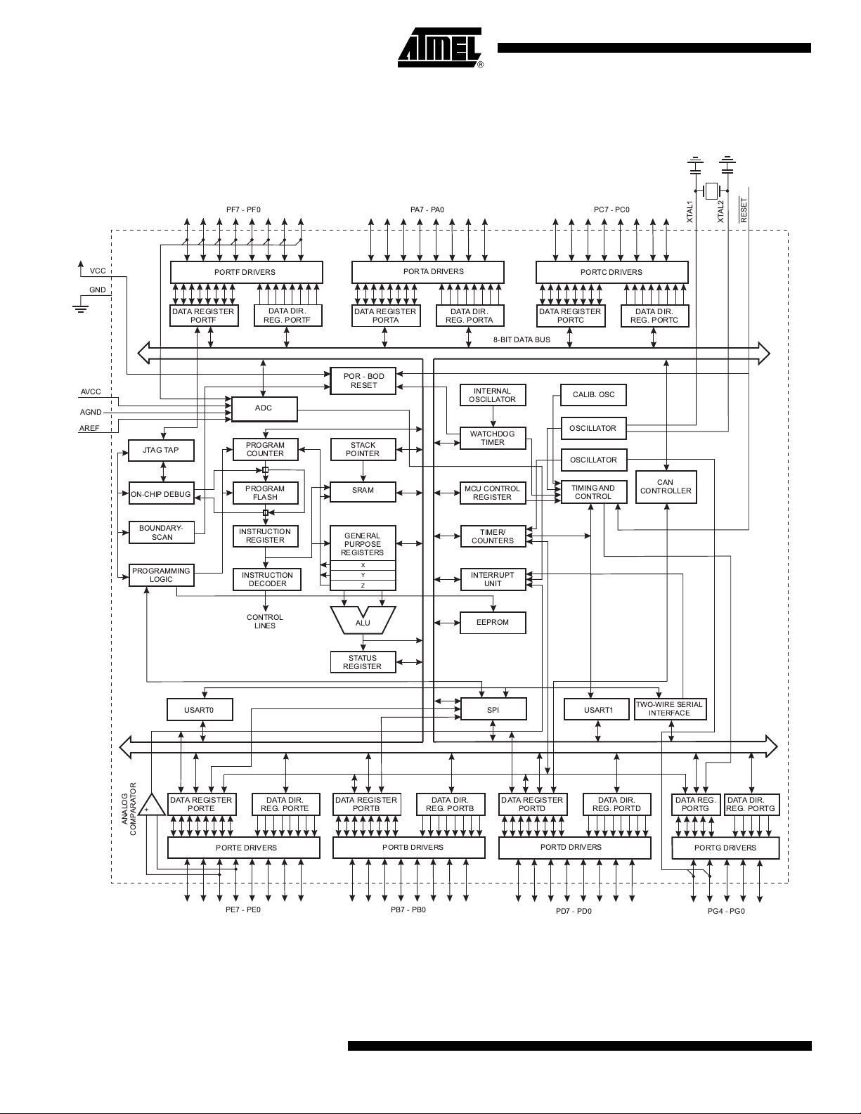
1.3 Block Diagram
PROGRAM
COUNTER
STACK
POINTER
PROGRAM
FLASH
MCU CONTROL
REGISTER
SRAM
GENERAL
PURPOSE
REGISTERS
INSTRUCTION
REGISTER
TIMER/
COUNTERS
INSTRUCTION
DECODER
DATA DIR.
REG. PORTB
DATA DIR.
REG. PORTE
DATA DIR.
REG. PORTA
DATA DIR.
REG. PORTD
DATA REGISTER
PORTB
DATA REGISTER
PORTE
DATA REGISTER
PORTA
DATAREGISTER
PORTD
INTERRUPT
UNIT
EEPROM
SPIUSART0
STATUS
REGISTER
Z
Y
X
ALU
PORTB DRIVERS
PORTE DRIVERS
PORTA DRIVERS
PORTF DRIVERS
PORTD DRIVERS
PORTC DRIVERS
PB7 - PB0PE7 - PE0
PA7 - PA0PF7 - PF0
RESET
VCC
AGND
GND
AREF
XTAL1
XTAL2
CONTROL
LINES
+
-
ANALOG
COMPARATOR
PC7 - PC0
INTERNAL
OSCILLATOR
WATCHDOG
TIMER
8-BIT DATA BUS
AVCC
USART1
TIMING AND
CONTROL
OSCILLATOR
OSCILLATOR
CALIB. OSC
DATA DIR.
REG. PORTC
DATA REGISTER
PORTC
ON-CHIP DEBUG
JTAG TAP
PROGRAMMING
LOGIC
BOUNDARY-
SCAN
DATA DIR.
REG. PORTF
DATA REGISTER
PORTF
ADC
POR - BOD
RESET
PD7 - PD0
DATA DIR.
REG. PORTG
DATAREG.
PORTG
PORTG DRIVERS
PG4 - PG0
TWO-WIRE SERIAL
INTERFACE
CAN
CONTROLLER
Figure 1-1. Block Diagram
4
AT90CAN32/64/128
7679BS–CAN–11/06
Page 5
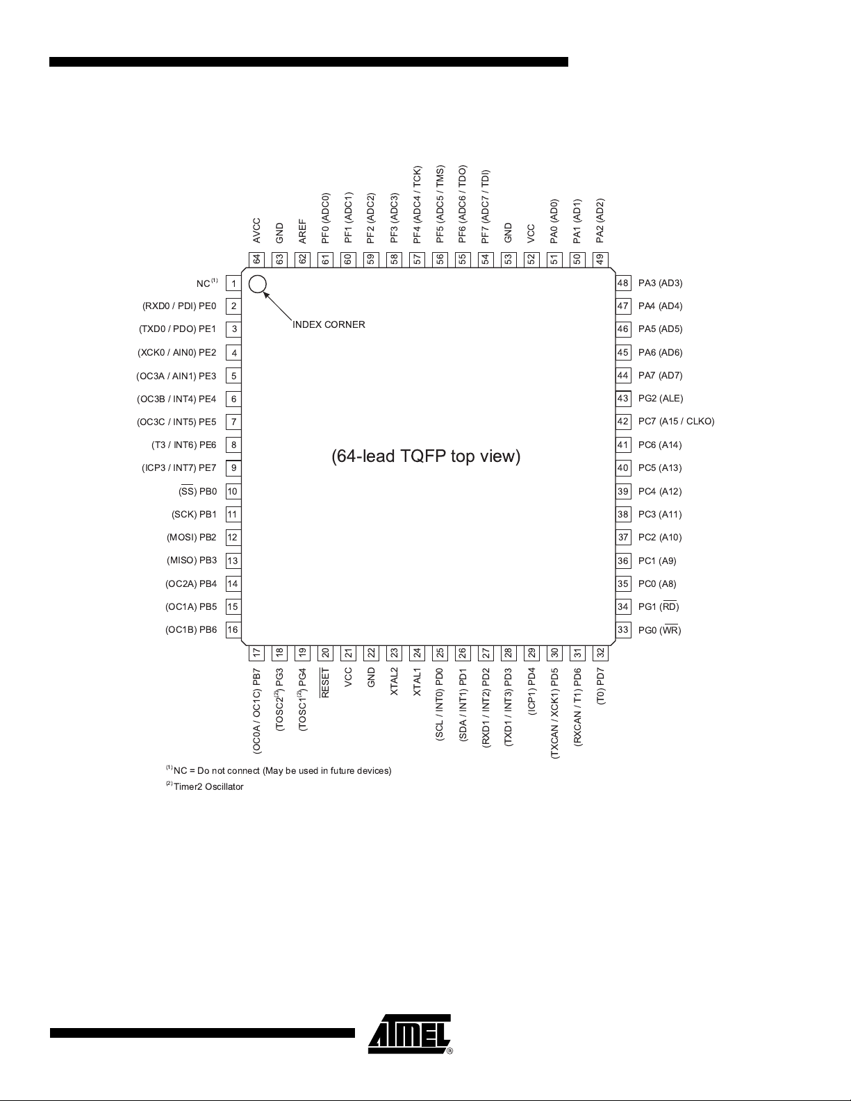
1.4 Pin Configurations
PC0 (A8)
VCC
GND
PF0 (ADC0)
PF7 (ADC7 / TDI)
PF1 (ADC1)
PF2 (ADC2)
PF3 (ADC3)
PF4 (ADC4 / TCK)
PF5 (ADC5 / TMS)
PF6 (ADC6 / TDO)
AREF
GND
AVCC
17
61
60
18
592058
19
21
572256
235524
54
25
532652
27
51
29
28
50
49
32
31
30
(RXD0 / PDI) PE0
(TXD0 / PDO) PE1
(XCK0 / AIN0) PE2
(OC3A / AIN1) PE3
(OC3B / INT4) PE4
(OC3C / INT5) PE5
(T3 / INT6) PE6
(ICP3 / INT7) PE7
(SS) PB0
(SCK) PB1
(MOSI) PB2
(MISO) PB3
(OC2A) PB4
(OC0A / OC1C) PB7
(TOSC2 ) PG3
(OC1B) PB6
(TOSC1 ) PG4
(OC1A) PB5
PC1 (A9)
(T0) PD7
PC2 (A10)
PC3 (A11)
PC4 (A12)
PC5 (A13)
PC6 (A14)
PC7 (A15 / CLKO)
PA7 (AD7)
PG2 (ALE)
PA6 (AD6)
PA5 (AD5)
PA4 (AD4)
PA3 (AD3)
PA0 (AD0)
PA1 (AD1)
PA2 (AD2)
(RXCAN / T1) PD6
(TXCAN / XCK1) PD5
(ICP1) PD4
(TXD1 / INT3) PD3
(RXD1 / INT2) PD2
(SDA / INT1) PD1
(SCL / INT0) PD0
XTAL1
XTAL2
RESET
GND
VCC
PG1 (RD)
PG0 (WR)
2
3
1
4
5
6
7
8
9
10
11
12
13
14
16
15
64
63
62
47
46
48
45
44
43
42
41
40
39
38
37
36
35
33
34
(2)
(2)
NC = Do not connect (May be used in future devices)
(1)
Timer2 Oscillator
(2)
NC
(1)
(64-lead TQFP top view)
INDEX CORNER
Figure 1-2. Pinout AT90CAN32/64/128 - TQFP
AT90CAN32/64/128
7679BS–CAN–11/06
5
Page 6

Figure 1-3. Pinout AT90CAN32/64/128 - QFN
NC = Do not connect (May be used in future devices)
(1)
Timer2 Oscillator
(2)
PC0 (A8)
VCC
GND
PF0 (ADC0)
PF7 (ADC7 / TDI)
PF1 (ADC1)
PF2 (ADC2)
PF3 (ADC3)
PF4 (ADC4 / TCK)
PF5 (ADC5 / TMS)
PF6 (ADC6 / TDO)
AREF
GND
AVCC
(RXD0 / PDI) PE0
(TXD0 / PDO) PE1
(XCK0 / AIN0) PE2
(OC3A / AIN1) PE3
(OC3B / INT4) PE4
(OC3C / INT5) PE5
(T3 / INT6) PE6
(ICP3 / INT7) PE7
(SS) PB0
(SCK) PB1
(MOSI) PB2
(MISO) PB3
(OC2A) PB4
(OC0A / OC1C) PB7
(TOSC2 ) PG3
(OC1B) PB6
(TOSC1 ) PG4
(OC1A) PB5
PC1 (A9)
(T0) PD7
PC2 (A10)
PC3 (A11)
PC4 (A12)
PC5 (A13)
PC6 (A14)
PC7 (A15 / CLKO)
PA7 (AD7)
PG2 (ALE)
PA6 (AD6)
PA5 (AD5)
PA4 (AD4)
PA3 (AD3)
PA0 (AD0)
PA1 (AD1)
PA2 (AD2)
(RXCAN / T1) PD6
(TXCAN / XCK1) PD5
(ICP1) PD4
(TXD1 / INT3) PD3
(RXD1 / INT2) PD2
(SDA / INT1) PD1
(SCL / INT0) PD0
XTAL1
XTAL2
RESET
GND
VCC
PG1 (RD)
PG0 (WR)
2
3
1
4
5
6
7
8
9
10
11
12
13
14
16 33
15
47
46
48
45
44
43
42
41
40
39
38
37
36
35
34
(2)
(2)
NC
(1)
17
182019
21222324252627
29
28
32
31
30
525150
49
6463625361605958575655
54
(64-lead QFN top view)
INDEX CORNER
6
AT90CAN32/64/128
Note: The large center pad underneath the QFN package is made of metal and internally connected to
GND. It should be soldered or glued to the board to ensure good mechanical stability. If the center
pad is left unconnected, the package might loosen from the board.
7679BS–CAN–11/06
Page 7

1.5 Pin Descriptions
1.5.1 VCC
Digital supply voltage.
1.5.2 GND
Ground.
1.5.3 Port A (PA7..PA0)
Port A is an 8-bit bi-directional I/O port with internal pull-up resistors (selected for each bit). The
Port A output buffers have symmetrical drive characteristics with both high sink and source
capability. As inputs, Port A pins that are externally pulled low will source current if the pull-up
resistors are activated. The Port A pins are tri-stated when a reset condition becomes active,
even if the clock is not running.
Port A also serves the functions of various special features of the AT90CAN32/64/128 as listed
on I/O-Ports paragraph of the complete Datasheet.
1.5.4 Port B (PB7..PB0)
Port B is an 8-bit bi-directional I/O port with internal pull-up resistors (selected for each bit). The
Port B output buffers have symmetrical drive characteristics with both high sink and source
capability. As inputs, Port B pins that are externally pulled low will source current if the pull-up
resistors are activated. The Port B pins are tri-stated when a reset condition becomes active,
even if the clock is not running.
AT90CAN32/64/128
Port B also serves the functions of various special features of the AT90CAN32/64/128 as listed
on I/O-Ports paragraph of the complete Datasheet.
1.5.5 Port C (PC7..PC0)
Port C is an 8-bit bi-directional I/O port with internal pull-up resistors (selected for each bit). The
Port C output buffers have symmetrical drive characteristics with both high sink and source
capability. As inputs, Port C pins that are externally pulled low will source current if the pull-up
resistors are activated. The Port C pins are tri-stated when a reset condition becomes active,
even if the clock is not running.
Port C also serves the functions of special features of the AT90CAN32/64/128 as listed on I/OPorts paragraph of the complete Datasheet.
1.5.6 Port D (PD7..PD0)
Port D is an 8-bit bi-directional I/O port with internal pull-up resistors (selected for each bit). The
Port D output buffers have symmetrical drive characteristics with both high sink and source
capability. As inputs, Port D pins that are externally pulled low will source current if the pull-up
resistors are activated. The Port D pins are tri-stated when a reset condition becomes active,
even if the clock is not running.
Port D also serves the functions of various special features of the AT90CAN32/64/128 as listed
on I/O-Ports paragraph of the complete Datasheet.
1.5.7 Port E (PE7..PE0)
Port E is an 8-bit bi-directional I/O port with internal pull-up resistors (selected for each bit). The
Port E output buffers have symmetrical drive characteristics with both high sink and source
capability. As inputs, Port E pins that are externally pulled low will source current if the pull-up
7679BS–CAN–11/06
7
Page 8

resistors are activated. The Port E pins are tri-stated when a reset condition becomes active,
even if the clock is not running.
Port E also serves the functions of various special features of the AT90CAN32/64/128 as listed
on I/O-Ports paragraph of the complete Datasheet.
1.5.8 Port F (PF7..PF0)
Port F serves as the analog inputs to the A/D Converter.
Port F also serves as an 8-bit bi-directional I/O port, if the A/D Converter is not used. Port pins
can provide internal pull-up resistors (selected for each bit). The Port F output buffers have symmetrical drive characteristics with both high sink and source capability. As inputs, Port F pins
that are externally pulled low will source current if the pull-up resistors are activated. The Port F
pins are tri-stated when a reset condition becomes active, even if the clock is not running.
Port F also serves the functions of the JTAG interface. If the JTAG interface is enabled, the pullup resistors on pins PF7(TDI), PF5(TMS), and PF4(TCK) will be activated even if a reset occurs.
1.5.9 Port G (PG4..PG0)
Port G is a 5-bit I/O port with internal pull-up resistors (selected for each bit). The Port G output
buffers have symmetrical drive characteristics with both high sink and source capability. As
inputs, Port G pins that are externally pulled low will source current if the pull-up resistors are
activated. The Port G pins are tri-stated when a reset condition becomes active, even if the clock
is not running.
1.5.10 RESET
1.5.11 XTAL1
1.5.12 XTAL2
1.5.13 AVCC
1.5.14 AREF
Port G also serves the functions of various special features of the AT90CAN32/64/128 as listed
on I/O-Ports paragraph of the complete Datasheet.
Reset input. A low level on this pin for longer than the minimum pulse length will generate a
reset. The minimum pulse length is given in characteristics. Shorter pulses are not guaranteed
to generate a reset. The I/O ports of the AVR are immediately reset to their initial state even if
the clock is not running. The clock is needed to reset the rest of the AT90CAN32/64/128.
Input to the inverting Oscillator amplifier and input to the internal clock operating circuit.
Output from the inverting Oscillator amplifier.
AVCC is the supply voltage pin for the A/D Converter on Port F. It should be externally connected to VCC, even if the ADC is not used. If the ADC is used, it should be connected to V
through a low-pass filter.
This is the analog reference pin for the A/D Converter.
CC
8
AT90CAN32/64/128
7679BS–CAN–11/06
Page 9

AT90CAN32/64/128
2. Register Summary
Address Name Bit 7 Bit 6 Bit 5 Bit 4 Bit 3 Bit 2 Bit 1 Bit 0 Comment
(0xFF) Reserved
(0xFE) Reserved
(0xFD) Reserved
(0xFC) Reserved
(0xFB) Reserved
(0xFA) CANMSG MSG 7 MSG 6 MSG 5 MSG 4 MSG 3 MSG 2 MSG 1 MSG 0
(0xF9) CANSTMH TIMSTM15 TIMSTM14 TIMSTM13 TIMSTM12 TIMSTM11 TIMSTM10 TIMSTM9 TIMSTM8
(0xF8) CANSTML TIMSTM7 TIMSTM6 TIMSTM5 TIMSTM4 TIMSTM3 TIMSTM2 TIMSTM1 TIMSTM0
(0xF7) CANIDM1
(0xF6) CANIDM2
(0xF5) CANIDM3
(0xF4) CANIDM4
(0xF3) CANIDT1
(0xF2) CANIDT2
(0xF1) CANIDT3
(0xF0) CANIDT4
(0xEF) CANCDMOB CONMOB1 CONMOB0 RPLV IDE DLC3 DLC2 DLC1 DLC0
(0xEE) CANSTMOB DLCW TXOK RXOK BERR SERR CERR FERR AERR
(0xED) CANPAGE MOBNB3 MOBNB2 MOBNB1 MOBNB0 AINC INDX2 INDX1 INDX0
(0xEC) CANHPMOB HPMOB3 HPMOB2 HPMOB1 HPMOB0 CGP3 CGP2 CGP1 CGP0
(0xEB) CANREC REC7 REC6 REC5 REC4 REC3 REC2 REC1 REC0
(0xEA) CANTEC TEC7 TEC6 TEC5 TEC4 TEC3 TEC2 TEC1 TEC0
(0xE9) CANTTCH TIMTTC15 TIMTTC14 TIMTTC13 TIMTTC12 TIMTTC11 TIMTTC10 TIMTTC9 TIMTTC8
(0xE8) CANTTCL TIMTTC7 TIMTTC6 TIMTTC5 TIMTTC4 TIMTTC3 TIMTTC2 TIMTTC1 TIMTTC0
(0xE7) CANTIMH CANTIM15 CANTIM14 CANTIM13 CANTIM12 CANTIM11 CANTIM10 CANTIM9 CANTIM8
(0xE6) CANTIML CANTIM7 CANTIM6 CANTIM5 CANTIM4 CANTIM3 CANTIM2 CANTIM1 CANTIM0
(0xE5) CANTCON TPRSC7 TPRSC6 TPRSC5 TPRSC4 TPRSC3 TPRSC2 TRPSC1 TPRSC0
(0xE4) CANBT3 – PHS22 PHS21 PHS20 PHS12 PHS11 PHS10 SMP
(0xE3) CANBT2 – SJW1 SJW0 – PRS2 PRS1 PRS0 –
(0xE2) CANBT1 – BRP5 BRP4 BRP3 BRP2 B RP1 BRP0 –
(0xE1) CANSIT1 – SIT14 SIT13 SIT12 SIT11 SIT10 SIT9 SIT8
(0xE0) CANSIT2 SIT7 SIT6 SIT5 SIT4 SIT3 SIT2 SIT1 SIT0
(0xDF) CANIE1 – IEMOB14 IEMOB13 IEMOB12 IEMOB11 IEMOB10 IEMOB9 IEMOB8
(0xDE) CANIE2 IEMOB7 IEMOB6 IEMOB5 IEMOB4 IEMOB3 IEMOB2 IEMOB1 IEMOB0
(0xDD) CANEN1 – ENMOB14 ENMOB13 ENMOB12 ENMOB11 ENMOB10 ENMOB9 ENMOB8
(0xDC) CANEN2 ENMOB7 ENMOB6 ENMOB5 ENMOB4 ENMOB3 ENMOB2 ENMOB1 ENMOB0
(0xDB) CANGIE ENIT ENBOFF ENRX ENTX ENERR ENBX ENERG ENOVRT
(0xDA) CANGIT CANIT BOFFIT OVRTIM BXOK SERG CERG FERG AERG
(0xD9) CANGSTA – OVRG – TXBSY RXBSY ENFG BOFF ERRP
(0xD8) CANGCON ABRQ OVRQ TTC SYNTTC LISTEN TEST ENA/STB SWRES
(0xD7) Reserved
(0xD6) Reserved
(0xD5) Reserved
(0xD4) Reserved
(0xD3) Reserved
(0xD2) Reserved
(0xD1) Reserved
(0xD0) Reserved
(0xCF) Reserved
(0xCE) UDR1 UDR17 UDR16 UDR15 UDR14 UDR13 UDR12 UDR11 UDR10
(0xCD) UBRR1H – – – – UBRR111 UBRR110 UBRR19 UBRR18
(0xCC) UBRR1L UBRR17 UBRR16 UBRR15 UBRR14 UBRR13 UBRR12 UBRR11 UBRR10
(0xCB) Reserved
(0xCA) UCSR1C – UMSEL1 UPM11 UPM10 USBS1 UCSZ11 UCSZ10 UCPOL1
(0xC9) UCSR1B RXCIE1 TXCIE1 UDRIE1 RXEN1 TXEN1 UCSZ12 RXB81 TXB81
(0xC8) UCSR1A RXC1 TXC1 UDRE1 FE1 DOR1 UPE1 U2X1 MPCM1
(0xC7) Reserved
(0xC6) UDR0 UDR07 UDR06 UDR05 UDR04 UDR03 UDR02 UDR01 UDR00
(0xC5) UBRR0H – – – – UBRR011 UBRR010 UBRR09 UBRR08
(0xC4) UBRR0L UBRR07 UBRR06 UBRR05 UBRR04 UBRR03 UBRR02 UBRR01 UBRR00
(0xC3) Reserved
(0xC2) UCSR0C – UMSEL0 UPM01 UPM00 USBS0 UCSZ01 UCSZ00 UCPOL0
(0xC1) UCSR0B RXCIE0 TXCIE0 UDRIE0 RXEN0 TXEN0 UCSZ02 RXB80 TXB80
(0xC0) UCSR0A RXC0 TXC0 UDRE0 FE0 DOR0 UPE0 U2X0 MPCM0
(0xBF) Reserved
IDMSK
IDMSK
IDMSK
IDMSK
IDT
IDT
IDT
IDT
28
IDMSK
27
IDMSK
26
IDMSK
25
IDMSK
24
IDMSK
23
IDMSK
20
IDMSK
19
IDMSK
18
IDMSK
17
IDMSK
16
IDMSK
12
IDMSK
11
IDMSK
4
IDMSK
28
20
12
4
IDT
IDT
IDT
IDT
3
27
19
11
3
IDMSK
IDT
IDT
IDT
IDT
10
26
18
10
2
IDMSK
9
IDMSK
2
IDMSK
1
IDT
25
IDT
17
IDT
9
IDT
1
8
IDMSK
0 RTRMSK – IDEMSK
IDT
24
IDT
16
IDT
8
IDT
0 RTRTAG RB1TAG RB0TAG
IDMSK
IDT
IDT
IDT
15
7
23
15
7
IDMSK
IDMSK
IDT
IDT
IDT
22
14
22
14
6
IDMSK
21
IDMSK
6
IDMSK
IDT
IDT
IDT
13
5
21
13
5
7679BS–CAN–11/06
9
Page 10

Address Name Bit 7 Bit 6 Bit 5 Bit 4 Bit 3 Bit 2 Bit 1 Bit 0 Comment
(0xBE) Reserved
(0xBD) Reserved
(0xBC) TWCR TWINT TWEA TWSTA TWSTO TWWC TWEN – TWIE
(0xBB) TWDR TWDR7 TWDR6 TWDR5 TWDR4 TWDR3 TWDR2 TWDR1 TWDR0
(0xBA) TWAR TWAR6 TWAR5 TWAR4 TWAR3 TWAR2 TWAR1 TWAR0 TWGCE
(0xB9) TWSR TWS7 TWS6 TWS5 TWS4 TWS3 – TWPS1 TWPS0
(0xB8) TWBR TWBR7 TWBR6 TWBR5 TWBR4 TWBR3 TWBR2 TWBR1 TWBR0
(0xB7) Reserved
(0xB6) ASSR – – – EXCLK AS2 TCN2UB OCR2UB TCR2UB
(0xB5) Reserved
(0xB4) Reserved
(0xB3) OCR2A OCR2A7 OCR2A6 OCR2A5 OCR2A4 OCR2A3 OCR2A2 OCR2A1 OCR2A0
(0xB2) TCNT2 TCNT27 TCNT26 TCNT25 TCNT24 TCNT23 TCNT22 TCNT21 TCNT20
(0xB1) Reserved
(0xB0) TCCR2A FOC2A WGM20 COM2A1 COM2A0 WGM21 CS22 CS21 CS20
(0xAF) Reserved
(0xAE) Reserved
(0xAD) Reserved
(0xAC) Reserved
(0xAB) Reserved
(0xAA) Reserved
(0xA9) Reserved
(0xA8) Reserved
(0xA7) Reserved
(0xA6) Reserved
(0xA5) Reserved
(0xA4) Reserved
(0xA3) Reserved
(0xA2) Reserved
(0xA1) Reserved
(0xA0) Reserved
(0x9F) Reserved
(0x9E) Reserved
(0x9D) OCR3CH OCR3C15 OCR3C14 OCR3C13 OCR3C12 OCR3C11 OCR3C10 OCR3C9 OCR3C8
(0x9C) OCR 3CL OCR3C7 OCR3C6 OCR3C5 OCR3C4 OCR3C3 OCR3C2 OCR3C1 OCR3C0
(0x9B) OCR3BH OCR3B15 OCR3B14 OCR3B13 OCR3B12 OCR3B11 OCR3B10 OCR3B9 OCR3B8
(0x9A) OCR3BL OCR3B7 OCR3B6 OCR3B5 OCR3B4 OCR3B3 OCR3B2 OCR3B1 OCR3B0
(0x99) OCR3AH OCR3A15 OCR3A14 OCR3A13 OCR3A12 OCR3A11 OCR3A10 OCR3A9 OCR3A8
(0x98) OCR3AL OCR3A7 OCR3A6 OCR3A5 OCR3A4 OCR3A3 OCR3A2 OCR3A1 OCR3A0
(0x97) ICR3H ICR315 ICR314 ICR313 ICR312 ICR311 ICR310 ICR39 ICR 38
(0x96) ICR3L ICR37 ICR36 ICR35 ICR34 ICR33 ICR32 ICR31 ICR30
(0x95) TCNT3H TCNT315 TCNT314 TCNT313 TCNT312 TCNT311 TCNT310 TCNT39 TCNT38
(0x94) TCNT3L TCNT37 TCNT36 TCNT35 TCNT34 TCNT33 TCNT32 TCNT31 TCNT30
(0x93) Reserved
(0x92) TCCR3C FOC3A FOC3B FOC3C – – – –
(0x91) TCCR3B ICNC3 ICES3 – WGM33 WGM32 CS32 CS31 CS30
(0x90) TCCR3A COM3A1 COM3A0 COM3B1 COM3B0 COM3C1 COM3C0 WGM31 WGM30
(0x8F) Reserved
(0x8E) Reserved
(0x8D) OCR1CH OCR1C15 OCR1C14 OCR1C13 OCR1C12 OCR1C11 OCR1C10 OCR1C9 OCR1C8
(0x8C) OCR 1CL OCR1C7 OCR1C6 OCR1C5 OCR1C4 OCR1C3 OCR1C2 OCR1C1 OCR1C0
(0x8B) OCR1BH OCR1B15 OCR1B14 OCR1B13 OCR1B12 OCR1B11 OCR1B10 OCR1B9 OCR1B8
(0x8A) OCR1BL OCR1B7 OCR1B6 OCR1B5 OCR1B4 OCR1B3 OCR1B2 OCR1B1 OCR1B0
(0x89) OCR1AH OCR1A15 OCR1A14 OCR1A13 OCR1A12 OCR1A11 OCR1A10 OCR1A9 OCR1A8
(0x88) OCR1AL OCR1A7 OCR1A6 OCR1A5 OCR1A4 OCR1A3 OCR1A2 OCR1A1 OCR1A0
(0x87) ICR1H ICR115 ICR114 ICR113 ICR112 ICR111 ICR110 ICR19 ICR 18
(0x86) ICR1L ICR17 ICR16 ICR15 ICR14 ICR13 ICR12 ICR11 ICR10
(0x85) TCNT1H TCNT115 TCNT114 TCNT113 TCNT112 TCNT111 TCNT110 TCNT19 TCNT18
(0x84) TCNT1L TCNT17 TCNT16 TCNT15 TCNT14 TCNT13 TCNT12 TCNT11 TCNT10
(0x83) Reserved
(0x82) TCCR1C FOC1A FOC1B FOC1C – – – – –
(0x81) TCCR1B ICNC1 ICES1 – WGM13 WGM12 CS12 CS11 CS10
(0x80) TCCR1A COM1A1 COM1A0 COM1B1 COM1B0 COM1C1 COM1C0 WGM11 WGM10
(0x7F) DIDR1 – – – – – – AIN1D AIN0D
(0x7E) DIDR0 ADC7D ADC6D ADC5D ADC4D ADC3D ADC2D ADC1D ADC0D
(0x7D) Reserved
10
AT90CAN32/64/128
7679BS–CAN–11/06
Page 11

AT90CAN32/64/128
Address Name Bit 7 Bit 6 Bit 5 Bit 4 Bit 3 Bit 2 Bit 1 Bit 0 Comment
(0x7C) ADMUX REFS1 REFS0 ADLAR MUX4 MUX3 MUX2 MUX1 MUX0
(0x7B) ADCSRB – ACME – – – ADTS2 ADTS1 ADTS0
(0x7A) ADCSRA ADEN ADSC ADATE ADIF ADIE ADPS2 ADPS1 ADPS0
(0x79) ADCH - / ADC9 - / ADC8 - / ADC7 - / ADC6 - / ADC5 - / ADC4 ADC9 / ADC3 ADC8 / ADC2
(0x78) ADCL ADC7 / ADC1 ADC6 / ADC0 ADC5 / - ADC4 / - ADC3 / - ADC2 / - ADC1 / - ADC0 /
(0x77) Reserved
(0x76) Reserved
(0x75) XMCRB XMBK – – – – XMM2 XMM1 XMM0
(0x74) XMCRA SRE SRL2 SRL1 SRL0 SRW11 SRW10 SRW01 SRW00
(0x73) Reserved
(0x72) Reserved
(0x71) TIMSK3 – – ICIE3 – OCIE3C OCIE3B OCIE3A TOIE3
(0x70) TIMSK2 – – – – – – OCIE2A TOIE2
(0x6F) TIMSK1 – – ICIE1 – OCIE1C OCIE1B OCIE1A TOIE1
(0x6E) TIMSK0 – – – – – – OCIE0A TOIE0
(0x6D) Reserved
(0x6C) Reserved
(0x6B) Reserved
(0x6A) E ICRB ISC71 ISC70 ISC61 ISC60 ISC51 ISC50 ISC41 ISC40
(0x69) EICRA ISC31 ISC30 ISC21 ISC20 ISC11 ISC10 ISC01 ISC00
(0x68) Reserved
(0x67) Reserved
(0x66) OSCCAL – CAL6 CAL5 CAL4 CAL3 CAL2 CAL1 CAL0
(0x65) Reserved
(0x64) Reserved
(0x63) Reserved
(0x62) Reserved
(0x61) CLKPR CLKPCE – – – CLKPS3 CLKPS2 CLKPS1 CLKPS0
(0x60) WDTCR – – – WDCE WDE WDP2 WDP1 WDP0
0x3F (0x5F) SREG I T H S V N Z C
0x3E (0x5E) SPH SP15 SP14 SP13 SP12 SP11 SP10 SP9 SP8
0x3D (0x5D) SPL SP7 SP6 SP5 S P4 SP3 SP2 SP1 SP0
0x3C (0x5C) Reserved
0x3B (0x5B) RAMPZ – – – – – – – RAMPZ0
0x3A (0x5A) Reserved
0x39 (0x59) Reserved
0x38 (0x58) Reserved
0x37 (0x57) SPMCSR SPMIE RWWSB – RWWSRE BLBSET PGWRT PGERS SPMEN
0x36 (0x56) Reserved – – – – – – – –
0x35 (0x55) MCUCR JTD – – PUD – – IVSEL IVCE
0x34 (0x54) MCUSR – – – JTRF WDRF B ORF EXTRF PORF
0x33 (0x53) SMCR – – – – SM2 SM1 SM0 SE
0x32 (0x52) Reserved
0x31 (0x51) OCDR IDRD/OCDR7 OCDR6 OCDR5 OCDR4 OCDR3 OCDR2 OCDR1 OCDR0
0x30 (0x50) ACSR ACD ACBG ACO ACI ACIE ACIC ACIS1 ACIS0
0x2F (0x4F) Reserved
0x2E (0x4E) SPDR SPD7 SPD6 SPD5 SPD4 SPD3 SPD2 SPD1 SPD0
0x2D (0x4D) SPSR SPIF WCOL – – – – – SPI2X
0x2C (0x4C) SPCR SPIE SPE DORD MSTR CPOL CPHA SPR1 SPR0
0x2B (0x4B) GPIOR2 GPIOR27 GPIOR26 GPIOR25 GPIOR24 GPIOR23 GPIOR22 GPIOR21 GPIOR20
0x2A (0x4A) GPIOR1 GPIOR17 GPIOR16 GPIOR15 GPIOR14 GPIOR13 GPIOR12 GPIOR11 GPIOR10
0x29 (0x49) Reserved
0x28 (0x48) Reserved
0x27 (0x47) OCR0A OCR0A7 OCR0A6 OCR0A5 OCR0A4 OCR0A3 OCR0A2 OCR0A1 OCR0A0
0x26 (0x46) TCNT0 TCNT07 TCNT06 TCNT05 TCNT04 TCNT03 TCNT02 TCNT01 TCNT00
0x25 (0x45) Reserved
0x24 (0x44) TCCR0A FOC0A WGM00 COM0A1 COM0A0 WGM01 CS02 CS01 CS00
0x23 (0x43) GTCCR TSM – – – – – PSR2 PSR310
0x22 (0x42) EEARH – – – – EEAR11 EEAR10 EEAR9 EEAR8
0x21 (0x41) EEARL EEAR7 EEAR6 EEAR5 EEAR4 EEAR3 EEAR2 EEAR1 EEAR0
0x20 (0x40) EEDR EEDR7 EEDR6 EEDR5 EEDR4 EEDR3 EEDR2 EEDR1 EEDR0
0x1F (0x3F) EECR – – – – EERIE EEMWE EEWE EERE
0x1E (0x3E) GPIOR0 GPIOR07 GPIOR06 GPIOR05 GPIOR04 GPIOR03 GPIOR02 GPIOR01 GPIOR00
0x1D (0x3D) EIMSK INT7 INT6 INT5 INT4 INT3 INT2 INT1 INT0
0x1C (0x3C) EIFR INTF7 INTF6 INTF5 INTF4 INTF3 INTF2 INTF1 INTF0
0x1B (0x3B)
Reserved
(1)
(2)
7679BS–CAN–11/06
11
Page 12

Address Name Bit 7 Bit 6 Bit 5 Bit 4 Bit 3 Bit 2 Bit 1 Bit 0 Comment
0x1A (0x3A)
0x19 (0x39)
0x18 (0x38) TIFR3 – – ICF3 – OCF3C OCF3B OCF3A TOV3
0x17 (0x37) TIFR2 – – – – – – OCF2A TOV2
0x16 (0x36) TIFR1 – – ICF1 – OCF1C OCF1B OCF1A TOV1
0x15 (0x35) TIFR0 – – – – – – OCF0A TOV0
0x14 (0x34) PORTG – – – PORTG4 PORTG3 PORTG2 PORTG1 PORTG0
0x13 (0x33) DDRG – – – DDG4 DDG3 DDG2 DDG1 DDG0
0x12 (0x32) PING – – – PING4 PING3 PING2 PING1 PING0
0x11 (0x31) PORTF PORTF7 PORTF6 PORTF5 PORTF4 PORTF3 PORTF2 PORTF1 PORTF0
0x10 (0x30) DDRF DDF7 DDF6 DDF5 DDF4 DDF3 DDF2 DDF1 DDF0
0x0F (0x2F) PINF PINF7 PINF6 PINF5 PINF4 PINF3 PINF2 PINF1 PINF0
0x0E (0x2E) PORTE PORTE7 PORTE6 PORTE5 PORTE4 PORTE3 PORTE2 PORTE1 P ORTE0
0x0D (0x2D) DDRE DDE7 DDE6 DDE5 DDE4 DDE3 DDE2 DDE1 DDE0
0x0C (0x2C) PINE PINE7 PINE6 PINE5 PINE4 PINE3 PINE2 PINE1 PINE0
0x0B (0x2B) PORTD PORTD7 PORTD6 PORTD5 PORTD4 PORTD3 PORTD2 PORTD1 PORTD0
0x0A (0x2A) DDRD DDD7 DDD6 DDD5 DDD4 DDD3 DDD2 DDD1 DDD0
0x09 (0x29) PIND PIND7 PIND6 PIND5 PIND4 PIND3 PIND2 PIND1 PIND0
0x08 (0x28) PORTC PORTC7 P ORTC6 PORTC5 PORTC4 P ORTC3 PORTC2 PORTC1 PORTC0
0x07 (0x27) DDRC DDC7 DDC6 DDC5 DDC4 DDC3 DDC2 DDC1 DDC0
0x06 (0x26) PINC PINC7 PINC6 PINC5 PINC4 PINC3 PINC2 PINC1 PINC0
0x05 (0x25) PORTB PORTB7 PORTB6 P ORTB5 PORTB4 PORTB3 PORTB2 PORTB1 PORTB0
0x04 (0x24) DDRB DDB7 DDB6 DDB5 DDB4 DDB3 DDB2 DDB1 DDB0
0x03 (0x23) PINB PINB7 PINB6 PINB5 PINB4 PINB3 PINB2 PINB1 PINB0
0x02 (0x22) PORTA PORTA7 PORTA6 P ORTA5 PORTA4 PORTA3 PORTA2 PORTA1 PORTA0
0x01 (0x21) DDRA DDA7 DDA6 DDA5 DDA4 DDA3 DDA2 DDA1 DDA0
0x00 (0x20) PINA PINA7 PINA6 PINA5 PINA4 PINA3 PINA2 PINA1 PINA0
Reserved
Reserved
Notes: 1. Address bits exceeding PCMSB (c.f. complete Datasheet) are don’t care.
2. Address bits exceeding EEAMSB (c.f. complete Datasheet) are don’t care.
3. For compatibility with future devices, reserved bits should be written to zero if accessed. Reserved I/O memory addresses
should never be written.
4. I/O Registers within the address range 0x00 - 0x1F are directly bit-accessible using the SBI and CBI instructions. In these
registers, the value of single bits can be checked by using the SBIS and SBIC instructions.
5. Some of the status flags are cleared by writing a logical one to them. Note that, unlike most other AVRs, the CBI and SBI
instructions will only operate on the specified bit, and can therefore be used on registers containing such status flags. The
CBI and SBI instructions work with registers 0x00 to 0x1F only.
6. When using the I/O specific commands IN and OUT, the I/O addresses 0x00 - 0x3F must be used. When addressing I/O
Registers as data space using LD and ST instructions, 0x20 must be added to these addresses. The AT90CAN32/64/128 is
a complex microcontroller with more peripheral units than can be supported within the 64 location reserved in Opcode for
the IN and OUT instructions. For the Extended I/O space from 0x60 - 0xFF in SRAM, only the ST/STS/STD and
LD/LDS/LDD instructions can be used.
12
AT90CAN32/64/128
7679BS–CAN–11/06
Page 13

3. Ordering Information
AT90CAN32/64/128
Ordering Code
AT90CAN32-16AI 16 2.7 - 5.5 64A Industrial (-40° to +85°C) AT90CAN32-IL
AT90CAN32-16MI 16 2.7 - 5.5 64M1 Industrial (-40° to +85°C) AT90CAN32-IL
AT90CAN32-16AU 16 2.7 - 5.5 64A
AT90CAN32-16MU 16 2.7 - 5.5 64M1
AT90CAN64-16AI 16 2.7 - 5.5 64A Industrial (-40° to +85°C) AT90CAN64-IL
AT90CAN64-16MI 16 2.7 - 5.5 64M1 Industrial (-40° to +85°C) AT90CAN64-IL
AT90CAN64-16AU 16 2.7 - 5.5 64A
AT90CAN64-16MU 16 2.7 - 5.5 64M1
AT90CAN128-16AI 16 2.7 - 5.5 64A Industrial (-40° to +85°C) AT90CAN128-IL
AT90CAN128-16MI 16 2.7 - 5.5 64M1 Industrial (-40° to +85°C) AT90CAN128-IL
AT90CAN128-16AU 16 2.7 - 5.5 64A
AT90CAN128-16MU 16 2.7 - 5.5 64M1
(1)
Speed (MHz) Power Supply (V) Package Operation Range Product Marking
Industrial (-40° to +85°C)
Green
Industrial (-40° to +85°C)
Green
Industrial (-40° to +85°C)
Green
Industrial (-40° to +85°C)
Green
Industrial (-40° to +85°C)
Green
Industrial (-40° to +85°C)
Green
AT90CAN32-UL
AT90CAN32-UL
AT90CAN64-UL
AT90CAN64-UL
AT90CAN128-UL
AT90CAN128-UL
Notes: 1. These devices can also be supplied in wafer form. Please contact your local Atmel sales office for detailed ordering informa-
tion and minimum quantities.
4. Packaging Information
Package Type
64A 64-Lead, Thin (1.0 mm) Plastic Gull Wing Quad Flat Package (TQFP)
64M1 64-Lead, Quad Flat No lead (QFN)
7679BS–CAN–11/06
13
Page 14

4.1 TQFP64
14
AT90CAN32/64/128
7679BS–CAN–11/06
Page 15

4.2 QFN64
AT90CAN32/64/128
7679BS–CAN–11/06
15
Page 16

Atmel Corporation Atmel Operations
2325 Orchard Parkway
San Jose, CA 95131, USA
Tel: 1(408) 441-0311
Fax: 1(408) 487-2600
Regional Headquarters
Europe
Atmel Sarl
Route des Arsenaux 41
Case Postale 80
CH-1705 Fribourg
Switzerland
Tel: (41) 26-426-5555
Fax: (41) 26-426-5500
Asia
Room 1219
Chinachem Golden Plaza
77 Mody Road Tsim shatsui
Eas t Kowloon
Hong Kong
Tel: (852) 2721-9778
Fax: (852) 2722-1369
Japan
9F, Tonetsu Shinkawa Bldg.
1-24-8 Shinkawa
Chuo-ku, Tokyo 104-0033
Japan
Tel: (81) 3-3523-3551
Fax: (81) 3-3523-7581
Memory
2325 Orchard Parkway
San Jose, C A 95131, USA
Tel: 1(408) 441-0311
Fax: 1(408) 436-4314
Microcontrollers
2325 Orchard Parkway
San Jose, C A 95131, USA
Tel: 1(408) 441-0311
Fax: 1(408) 436-4314
La Chantrerie
BP 70602
44306 Nantes Cedex 3, France
Tel: (33) 2-40-18-18-18
Fax: (33) 2-40-18-19-60
ASIC/ASSP/Smart Cards
Zone Industrielle
13106 Rousset Cedex, France
Tel: (33) 4-42-53-60-00
Fax: (33) 4-42-53-60-01
1150 East Cheyenne Mtn. Blvd.
Colorado Springs, CO 80906, USA
Tel: 1(719) 576-3300
Fax: 1(719) 540-1759
Scottish Enterprise Tec hnology Park
Maxwell Building
Eas t Kilbride G75 0QR, Scotland
Tel: (44) 1355-803-000
Fax: (44) 1355-242-743
RF/Automotive
Theresienstrasse 2
Pos tfach 3535
74025 Heilbronn, Germany
Tel: (49) 71-31-67-0
Fax: (49) 71-31-67-2340
1150 East Cheyenne Mtn. Blvd.
Colorado Springs, CO 80906, USA
Tel: 1(719) 576-3300
Fax: 1(719) 540-1759
Biometrics/Imaging/Hi-Rel MPU/
High Speed Converters/RF Datacom
Avenue de R ochepleine
BP 123
38521 Saint-Egreve Cedex, France
Tel: (33) 4-76-58-30-00
Fax: (33) 4-76-58-34-80
Literature Requests
www.atmel.com/literature
Disclaimer: The information in this document is provided in con nec tio n with Atmel products. No license, express or implied, by estoppel or otherwise, to any
intellectual property right is granted by this document o r in c onnection with the sale of A tmel products. EXCEPT AS SET FORTH IN ATMEL’S TERMS AND CONDI-
TIONS OF SALE LOCATED ON ATMEL’S WEB SITE, ATMEL ASSUMES NO LIABILITY WHATSOEVER AND DISCLAIMS ANY EXPRESS, IMPLIED OR STATUTORY
WARRANTY RELATING TO ITS PRODUCTS INCLUDING, BUT NOT LIMITED TO, THE IMPLIED WARRANTY OF MERCHANTABILITY, FITNESS FOR A PARTICULAR
PURPOSE, OR NON-INFRINGEMENT. IN NO EVENT SHALL ATMEL BE LIABLE FOR ANY DIRECT, INDIRECT, CONSEQUENTIAL, PUNITIVE, SPECIAL OR INCIDENTAL DAMAGES (INCLUDING, WITHOUT LIMITATION, DAMAGES FOR LOSS OF PROFITS, BUSINESS INTERRUPTION, OR LOSS OF INFORMATION) ARISING OUT
OF THE USE OR INABILITY TO USE THIS DOCUMENT, EVEN IF ATMEL HAS BEEN ADVISED OF THE POSSIBILITY OF SUCH DAMAGES. Atmel makes no
repr esentations or wa rranti es w ith respec t to the accuracy or complete ness of the contents o f th is d ocu men t and reserves the right to make changes to spe cification s
and product descriptions at any t ime wit hou t no tic e. A tmel do es n ot make any commitmen t to update the inform ation contained herein. Unless specifical ly p rovidedotherwise, Atmel products are not suitable for, and shall not be used in, automotive applications. Atmel’sAtmel’s products are not intended, authorized, or warranted for use as
components in applications intended to support or sustain life.
© Atmel Corporation 2006. All rights reserved. A tmel®, logo and combinations thereof, are registered trademarks, and Ev erywhere You Are
are the trademarks of Atmel C orporation or its subsidiaries. Other terms and product names may be trademarks of others.
Printed on recycled paper.
7679BS–CAN–11/06
®
 Loading...