


AT89STK-10 Starter Kit
..............................................................................................
Hardware User Guide

Section 1
Introduction...........................................................................................1-2
1.1 Features....................................................................................................1-2
Section 2
Hardware Description.........................................................................2-10
Typical Applications............................................................................2-11
3.1 Nand Flash Application ...........................................................................2-12
3.2 Serial Dataflash Application....................................................................2-13
Section 3
Annex..................................................................................................3-14
4.1 Flash Evaluation Board................................... ....... ...... ....... ...... ....... ...... . 3 -1 5
4.2 Nand Flash Add-on board.......................................................................3-18
AT89STK-10 Starter Kit Hardware User User Guide 1
7534A–USB–07/05

This document descri bes the F lash E valuatio n Boa rd de dicated to the A T89C5 130/31A
and the AT8xC5122D USB microcontrollers. This board is designed to enable an easy
evaluation of the Mass Storage USB class using demonstration firmware (refer to firmware Guide). It must be plugged to a CPU board (AT89C5130/31A or AT8xC5122 D
evaluation board).
1.1 Features The Flash evaluation board provides the following features:
Support the following microcontrollers :
– AT89C5130A
– AT89C5131A
– AT8xC5122D
No external power supply required
– Power supplied by the USB line via the CPU board (AT89C5130/31A or
AT8xC5122 D evaluation board)
Section 1
Introduction
On board DataFlash memory (ATMEL AT45DB321B, 4MB)
Support Nand Flash memory (MICRON MT29F2GO8AABWP
board
Support Pluggable DataFlash Card (ATMEL AT45DCB004C,
AT89STK-10 Starter Kit Hardware User Guide 1-1
, 256MB) - Add-on
4 MB)
Rev. 7534A–USB–07/05
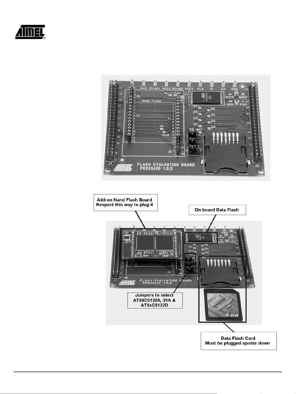
Figure 1-1. Flash Evaluation Board
Figure 1-2. Flash Evaluation Board with the related memories
AT89STK-10 Starter Kit Hardware User Guide 1-2
Rev. 7534A–USB–07/05
Hardware Description
Section 2
Hardware Description
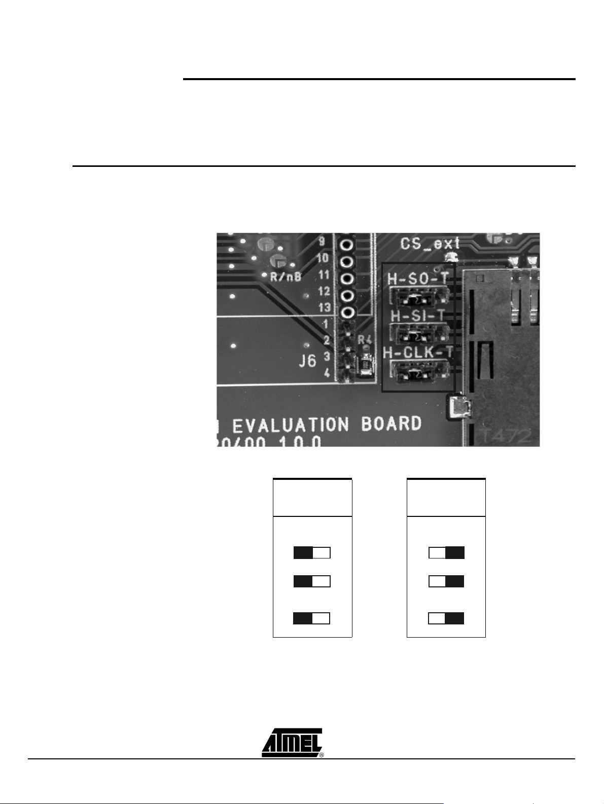
2.1 CPU board selection
As mentioned above, the Flash evaluation board can be used either with the
AT89C5130/31A or AT8xC5122 D. The figure below show the jumpers state to enable
each mode :
Figure 2-1. AT8xC5130/31AD Jumpers state
Figure 2-2. Jumpers state
AT89C5130A
AT89C5131A
(Default) AT89C5122D
H-SO-T
H-SI-T
H-CLK-T
The figures below show how to plug the Flash evaluation board to AT89C5130/31A or
AT8xC5122 D evaluation board (AT89STK05 or AT89STK03) :
AT89STK-10 Starter Kit Hardware User Guide 2-3
H-SO-T
H-SI-T
H-CLK-T
7534A–USB–07/05
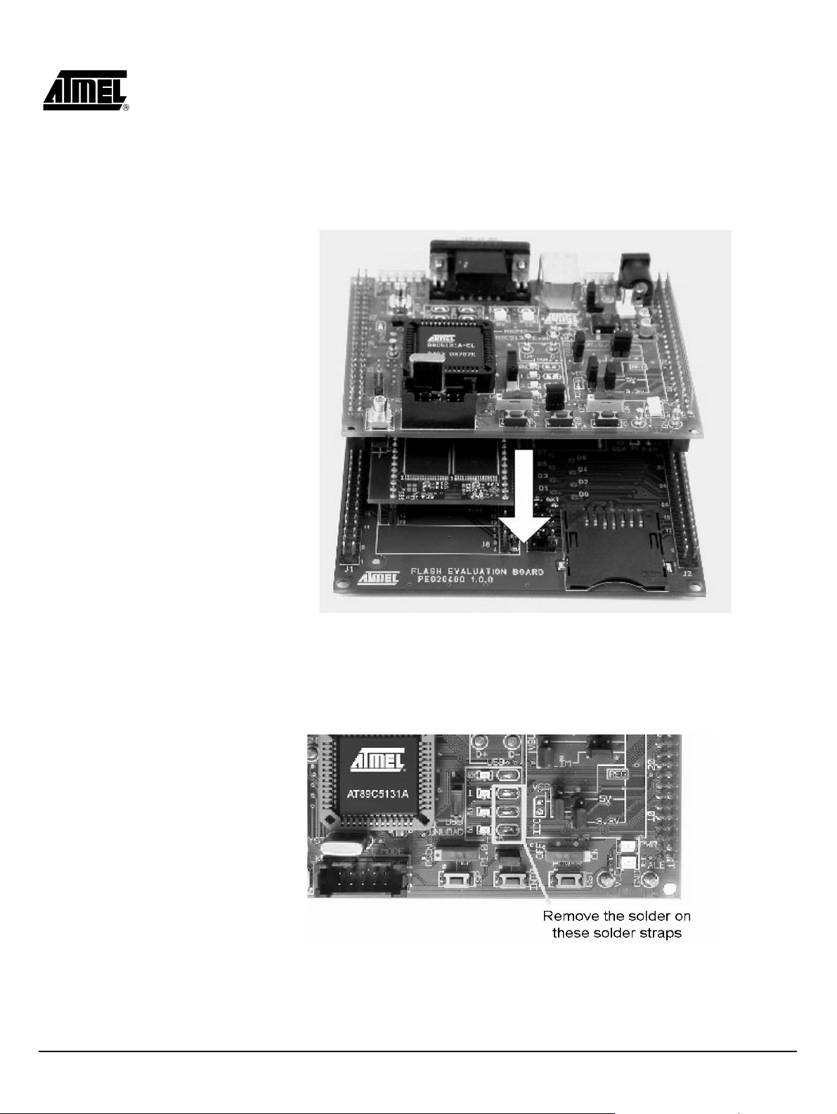
Figure 2-3. Flash evaluation board plugged to AT89C5130/31A evaluation board
(AT89STK05)
Warning : Before plugging the Flash Evoluation Board (AT89STK10) to the
AT89C5130/31A evalua tion board (AT89 STK05), di sconnect the thr ee LEDs by removing the solder on solder straps. The figure below shows the location of these solder
straps :
Figure 2-4. AT89STK-05 - LEDs Disconnection
AT89STK-10 Starter Kit Hardware User Guide 2-4
Rev. 7534A–USB–07/05

Hardware Description
Figure 2-5. Flash evaluation board plugged to AT8xC5122D evaluation board
(AT89STK03)
2.2 Power supply The Flash Evaluation Board power is supplied by the CPU board. The power supply must be set
to 3.3V for the AT89C5131A Evaluation board and 3.6V for th e AT8xC5122D Evaluation boar d.
The figure 2.5 s hows the differ ent possible co nfigurat ions of the AT89C5130/31A E valuation
board
(AT89STK05) and the figure 2.6 shows how to select 3.6V on the AT8xC5122D
Evaluation board in the 3.6V power supply configuration :
Figure 2-6. Power supply (3.3V) - AT89C5131A Evaluation Board (AT89STK05)
Power
Source
Regulation
Direct Input
3.3V Regulate
VBUS VBUS and
Current Limiter
PWR.S.
VCC
VCC
VBUS
LIM
ICC
PWR.S.
VBUS
LIM
ICC
REG
5V
3.3V
PWR
REG
5V
3.3V
PWR
VBUS
VCC
ICC
VBUS
VCC
ICC
PWR.S.
LIM
PWR.S.
LIM
PWR
PWR
5V
3.3V
5V
3.3V
REG
REG
VBUS
VCC
ICC
VBUS
VCC
ICC
External
PWR.S.
LIM
REG
5V
3.3V
PWR
PWR.S.
LIM
REG
5V
3.3V
PWR
AT89STK-10 Starter Kit Hardware User Guide 2-5
7534A–USB–07/05

Hardware Description
Figure 2-7. Power supply (3.6V)- AT8xC5122 D Evaluation Board (AT89STK03)
2.3 Memory selection
The Flash evaluation board supports three Flash memories (Pluggable Nand Flash,
Pluggable DataFlash Card and On board DataFlash). Just one memory can be activated at the same time.
To configure the board with your specific usage, you have to put the solder straps in the
right state.
Figure 2-8. Solder straps
“Open”
“Close”
Solder location
Figure 2-9. Solder Straps location
SP14
SP12
SP8
SP7
SP13
SP11
SP6
SP5
SP4
SP3
SP2
SP9
SP1
SP15
SP10
The tables hereunder show the configuration related to each memory mode :
2-6 AT89STK-10 Starter Kit Hardware User Guide
7534A–USB–07/05

Table 1. Nand Flash Configuration (Default configuration)
Reference Name Function State
SP1..8 D0..7 Connect Data P0 on onboard dataflash Open
SP9 CS Connect CS of internal dataflash Open
SP10 R/nB Connect R/nB on dataflash Open
SP 11 SER Select DataFlash in serial mode Open
SP12 PAR Select DataFlash in parallel mode Open
Hardware Description
SP 13 VccP
SP 14 GNDP
SP 15 CS_ext Connect CS of external dataflash Open
Connect power supply of parallel
interface of DataFlash
Connect ground of parallel interface of
DataFlash
Table 2. On Board DataFlash Configuration (Serial mode)
Reference Name Function State
SP1..8 D0..7 Connect bus P0 on onboard dataflash Open
SP9 CS Connect CS of internal dataflash Close
SP10 R/nB Connect R/nB on dataflash Close/Open
SP 11 SER Select DataFlash in serial mode Close
SP12 PAR S elect DataFlash in paralle l mode Open
SP 13 VccP
SP 14 GNDP
SP 15 CS_ext Connect CS of external dataflash Open
connect power supply of parallel
interface of DataFlash
connect gnd of parallel interface of
DataFlash
Open
Open
Open
Open
Table 3. On Board DataFlash Conf iguration (Parallel mode)
Reference Name Function State
SP1..8 D0..7 connect bus P0 on onboard dataflash Close
SP9 CS Connect CS of internal dataflash Close
SP10 R/nB Connect R/nB on dataflash Close
SP 11 SER put DataFlash in serial mode Open
SP12 PAR put DataFlash in paralle l mode Close
SP 13 VccP
SP 14 GNDP
SP 15 CS_ext Connect CS of external dataflash Open
connect power supply of parallel
interface of DataFlash
connect gnd of parallel interface of
DataFlash
Close
Close
The firmware doesn’t support this mode.
AT89STK-10 Starter Kit Hardware User Guide 2-7
7534A–USB–07/05

Hardware Description
Table 4. Pluggable DataFlash Card Configuration
Reference Name Function State
SP1..8 D0..7 connect bus P0 on onboard dataflash Open
SP9 CS Connect CS of internal dataflash Open
SP10 R/nB Connect R/nB on dataflash Open
SP 11 SER put DataFlash in serial mode Open
SP12 PAR put DataFlas h in parallel m ode Open
SP 13 VccP
SP 14 GNDP
connect power supply of parallel
interface of DataFlash
connect gnd of parallel interface of
DataFlash
Open
Open
SP 15 CS_ext Connect CS of external dataflash Close
2-8 AT89STK-10 Starter Kit Hardware User Guide
7534A–USB–07/05

Typical Applications
Section 3
Typical Applications
AT89STK-10 Starter Kit Hardware User Guide 3-9
7534A–USB–07/05

Typical Applications
3.1 Nand Flash Application
Vbus
D+
D-
GND
USB connector
optional
2.2k
ISP
3.3V
regulator
10nF 2.2nF
100
1.5k
22pF
100k
22pF
1µF
Vcc
Vcc
10µF
Tantal.
V DD AVDD
Vref
D+
27
D-
27
PLLF
PSEN
AT89C5131A-M
EA
P3.3
Xtal1
24
MHz
Xtal2
Ucap
AVss Vss
100nF
P0.0
P0.1
P0.2
P0.3
P0.4
P0.5
P0.6
P0.7
P2.4
P2.0
P2.1
P3.7
P2.3
P3.6
P3.0
Write
Protection
2.2k
Vcc
2.2k
Vcc
10µF
Tantal.
I/O.0
Vcc
I/O.1
I/O.2
I/O.3
I/O.4
I/O.5
I/O.6
I/O.7
10k
Nand Flash
WP
R/B
CLE
ALE
RE
CE
WE
Vss
3-10 AT89STK-10 Starter Kit Hardware User Guide
7534A–USB–07/05

3.2 Serial Dataflash Application
Vbus
D+
D-
GND
USB connector
optional
2.2k
ISP
3.3V
regulator
10nF 2.2nF
100
1.5k
22pF
100k
22pF
1µF
Vcc
Vcc
10µF
Tantal.
V DD AVDD
Vref
D+
27
D-
27
100nF
P0.0
P0.1
P0.2
P0.3
10µF
Tantal.
P0.4
PLLF
P0.5
P0.6
P0.7
Vcc
Write
Vcc
10k
10k
WP
Vcc
Reset
RDY/BUSY
CS
SCK/CLK
Data Flash
AT45DB321B
Vss
Vcc
SI
SO
SER/PAR
PSEN
AT89C5131A-M
EA
P3.3
Xtal1
24
MHz
Xtal2
Ucap
P2.4
P2.3
P1.6
P1.7/MOSI
P1.5/MISO
P3.0
AVss Vss
Protection
2.2k
AT89STK-10 Starter Kit Hardware User Guide 3-11
Rev. 7534A–USB–07/05

Annex
Section 4
Annex
4-12 AT89STK-10 Starter Kit Hardware User Guide
7534A–USB–07/05

4.1 Flash Evaluation Board
J5
J5
SER/nPAR
SO
CLK
SI
4
3
2
1
HE13 _4 FD
HE13 _4 FD
J3
J3
HE13 _13 FD
HE13 _13 FD
1
2
3
4
5
6
7
8
9
10
11
12
13
NF_nWP2
NF_nWP0
Vcc
NF_CLE
NF_ALE
NF_R/nB1
NF_nCE0
NF_R/nB0
NF_nCE1
NF_nRE
NF_nWE
nWP
nWP nWP
Vcc
CLE
ALE
R/nB1
nCE0
R/nB0
nCE1
nRE
nWE
nWP
P0_7
P0_6
P0_5
P0_4
P0_3
P0_2
P0_1
P0_0
Vss
NF_nWP3
NF_nWP1
NF_D7
NF_D6
NF_D5
NF_D4
NF_D3
NF_D2
NF_D1
NF_D0
J4
J4
1
2
3
4
5
6
7
8
9
10
11
12
13
HE13 _13 FD
HE13 _13 FD
J6
J6
HE13 _4 FD
HE13 _4 FD
Annex
1
P2_6
2
P2_7
3
C51_ALE
4
RESET
Vcc
R4
10 KR410 K
AT89STK-10 Starter Kit Hardware User Guide 4-13
7534A–USB–07/05

Annex
J2
J1
J1
J2
Vcc_CPU
Vcc
Vss
Vss
Vss Vss
Vss
Vss
47
Vss
45
43
41
39
37
35
33
31
29
Vss
27
25
Vss
23
21
19
17
15
13
11
9
7
5
Vss
3
Vss
1
HEADER 24X2
HEADER 24X2
flashboard Left
flashboard Left
Flash Board Left
48
46
44
42
40
38
36
34
32
30
28
26
24
22
20
18
16
14
12
10
8
6
4
2
P1_5
P1_6
P1_7
C51_ALE
_WE
_RE
MISO_T
CLK_T
MOSI_T
C51_ALE
nWE
nRE
TP8TP8
TP7TP7
TP6TP6
TP5TP5
TP4TP4
1
1
1
1
1
CLE ALE R/nB1 nCE0 R/nB0 nCE1 Vss
TP9TP9
P0_0
P0_1
P0_2
P0_3
P0_4
P0_5
P0_6
P0_7
CLE
ALE
R/nB1
nCE0
R/nB0
nCE1
P2_6
P2_7
MISO_H
MOSI_H
CLK_H
TP10TP10
1
1
P0_0
P0_1
P0_2
P0_3
P0_4
P0_5
P0_6
P0_7
P2_0
P2_1
P2_2
P2_3
P2_4
P2_5
P2_6
P2_7
P4_0
P4_1
P4_2
47
45
43
41
39
37
35
33
31
29
27
25
23
21
19
17
15
13
11
9
7
5
3
1
HEADER 24X2
HEADER 24X2
flashbord Right
flashbord Right
Flash Board Right
48
46
44
42
40
38
36
34
32
30
28
26
24
22
20
18
16
14
12
10
8
6
4
2
Vss
Vss
Vss
Vss
Vss
Vss
Vss
4-14 AT89STK-10 Starter Kit Hardware User Guide
7534A–USB–07/05

Annex
AT89STK-10 Starter Kit Hardware User Guide 4-15
7534A–USB–07/05

Annex
4.2 Nand Flash Addon board
Figure 4-1. Schematic
4-16 AT89STK-10 Starter Kit Hardware User Guide
7534A–USB–07/05

Figure 4-2. Component Side
Annex
Figure 4-3. Solder Side
AT89STK-10 Starter Kit Hardware User Guide 4-17
7534A–USB–07/05

Atmel Corporation Atmel Operations
2325 Orchard Parkway
San Jose, CA 95131
Tel: 1(408) 441-0311
Fax: 1(408) 487-2600
Regional Headquarters
Europe
Atmel Sarl
Route des Arsenaux 41
Case Postale 80
CH-1705 Fribourg
Switzerland
Tel: (41) 26-426-5555
Fax: (41) 26-426-5500
Asia
Room 1219
Chinachem Gol den P laza
77 Mody Road Tsimshatsui
East Kowloon
Hong Kong
Tel: (852) 2721-9778
Fax: (852) 2722-1369
Japan
9F, Tonetsu Shinkawa Bldg.
1-24-8 Shin kawa
Chuo-ku, Tokyo 104-0033
Japan
Tel: (81) 3-3523-3551
Fax: (81) 3-3523-7581
Memory
2325 Orchard Parkway
San Jose, CA 95131
Tel: 1(408) 441-0311
Fax: 1(408) 436-4314
Microcontrollers
2325 Orchard Parkway
San Jose, CA 95131
Tel: 1(408) 441-0311
Fax: 1(408) 436-4314
La Chantrerie
BP 70602
44306 Nantes Cedex 3, France
Tel: (33) 2- 40-1 8-18- 18
Fax: (33) 2- 40-18- 19-6 0
ASIC/ASSP/Smart Cards
Zone Industrielle
13106 Rousset Cedex, France
Tel: (33) 4- 42-5 3-60- 00
Fax: (33) 4- 42-53- 60-0 1
1150 East Cheyenne Mtn. Blvd.
Colorado Springs, CO 80906
Tel: 1(719) 576-3300
Fax: 1(719) 540-1759
Scottish Enterprise Technology Park
Maxwell Building
East Kilbride G75 0QR, Scotland
Tel: (44) 1355-803-000
Fax: (44) 1355-242-743
RF/Automotive
Theresienstrasse 2
Postfach 3535
74025 Heilbro nn, Ge rmany
Tel: (49) 71-31-67-0
Fax: (49) 71-31-67-2340
1150 East Cheyenne Mtn. Blvd.
Colorado Springs, CO 80906
Tel: 1(719) 576-3300
Fax: 1(719) 540-1759
Biometrics/Imaging/Hi-Rel MPU/
High Speed Converters/RF Datacom
Avenue de Rochepleine
BP 123
38521 Saint-Egreve Cedex, France
Tel: (33) 4-76-58-30-00
Fax: (33) 4- 76-58- 34-8 0
e-mail
literature@atmel.com
Web Site
http://www.atmel.com
Disclaimer: The information in this document is provided in connection with Atmel products. No license, express or implied, by estoppel or otherwise, to any
intellectual property right is granted by this document or in connection with the sale of A tmel products. EXCEPT AS SET FORTH IN ATMEL’S TERMS AND CONDI-
TIONS OF SALE LOCATED ON ATMEL’S WEB SITE, ATMEL ASSUMES NO LIABILITY WHATSOEVER AND DISCLAIMS ANY EXPRESS, IMPLIED OR STATUTORY
WARRANTY RELATING TO ITS PRODUCTS INCLUDING, BUT NOT LIMITED TO, THE IMPLIED WARRANTY OF MERCHANTABILITY, FITNESS FOR A PARTICULAR
PURPOSE, OR NON-INFRINGEMENT. IN NO EVENT SHALL ATMEL BE LIABLE FOR ANY DIRECT, INDIRECT, CONSEQUENTIAL, PUNITIVE, SPECIAL OR INCIDENTAL DAMAGES (INCLUDING, WITHOUT LIMITAT ION, DAMAGES FOR L OSS OF PROFITS, BUSINESS INT ERRUPTION, OR LOSS OF INF ORMATION) ARISING OUT
OF THE USE OR INABILITY TO USE THIS DOCUMENT, EVEN IF ATMEL HAS BEEN ADVISED OF THE POSSIBILITY OF SUCH DAMAGES. Atmel makes no
representations or warranties with respect to the accuracy or completeness of the contents of this document and reserves the right to make changes to specifications
and product descriptions at any time without notice. Atmel does not make any commitment to update the information contained herein. Unless specifically providedotherwise, Atmel produ cts are no t suitable for, and shall n ot be used in, automo tive app lications. Atmel’sAtmel’s pro ducts are not intende d, author ized, or warranted for use as
components in applications intended to support or sustain life.
© Atmel Corporation 2005. All rights reserved. Atmel®, logo and combinations thereof, are registered trademarks, and Everywhere You Are
are the trademarks of Atmel Corporation or its subsidiaries. Other terms and product names may be trademarks of others.
Printed on recycled paper.
7534A–USB–07/05
/xM
®
 Loading...