

Features
• Compatible with MCS-51
• 128K Bytes of In-System Reprogrammable Flash data memory and 4K Bytes of
Downloadable Flash Program Memory
– Endurance: 1,000 Write/Erase Cycles per Sector
– Data Retention: 10 Years
• Sector Programming: 128 Bytes/Sector
• Single 3.3V ±
± 10% Supply
±±
• On-Chip 12 MHz oscillator
• T wo-Level Pr o gr am Me mory Loc k
• 256-Bytes Internal RAM
• 5 Programmable I/O Lines
• Serial Peripheral Interface (SPI) Channel
• Serial Program Downloading
• Dual Data Pointer Registers
™
Products
AT89S4D12
8-Bit
Microcontroller
with
Description
The AT89S4D12 is a low-voltage, highly integrated CMOS 8-bit microcomputer with
4K bytes of downloadable Flash program memory and 128K bytes of in-system reprogrammable Flash data memory. The device is manufactured using Atmel’s high density Flash memory technology and is compatible with the industry-standard MCS-51
™
instruction set.
The 128K bytes of on-chip Fla sh data memory a re acc essed a s two 64K byte bloc ks.
Bit 0 at SFR location 96H is used to select the active block. The MOVX instruction is
used to read and write the data memory. Both the program and data memory arrays
can be programmed by an external programmer.
The downloadable Flash can be changed one page (128 bytes) at a time and is
accessible through the SPI serial peripher al interface port. Holding RESET active
forces the SPI bus into a slave input mode and allows the program memory to be written-from or read-to unless Lock Bit 2 has been activated.
The functional operations of the 128K bytes Flash data memory are equi valent to
those on the AT29LV010A 1M Bit Flash memory device.
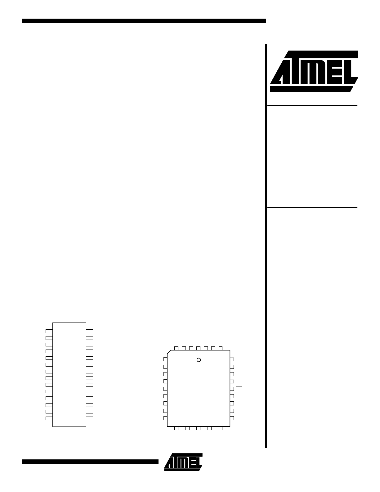
Pin Configurations
GND
TEST1
RESET
SDI/P1.1
SDO/P1.0
TEST2
NC
NC
NC
NC
NC
NC
NC
NC
SOIC Top View
1
2
3
4
5
6
7
8
9
10
11
12
13
14
28
27
26
25
24
23
22
21
20
19
18
17
16
15
VCC
P1.2/DTR
P1.3/SCK
P1.4/DSR
NC
NC
NC
NC
NC
NC
NC
NC
NC
NC
P1.0/SDO
TEST2
NC
NC
NC
NC
NC
NC
NC
PLCC Top View
P1.1/SDI
RESET
TEST1
GND
432
5
6
7
8
9
10
11
12
13
14151617181920
1
VCC
P1.2/DTR
P1.3/SCK
323130
29
28
27
26
25
24
23
22
21
P1.4/DSR
NC
NC
NC
NC
NC
NC
NC
NC
132K Bytes
Flash Data
Memory
AT89S4D12
NCNCNCNCNCNCNC
0921A-A–12/97
4-281
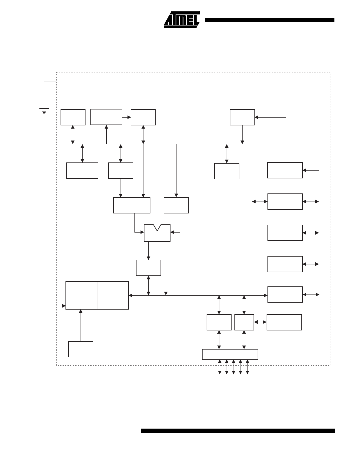
Block Diagram
V
CC
GND
128K
Flash
REGISTER
B
RAM ADDR.
REGISTER
RAM
ACC
TMP2 TMP1
ALU
PSW
STACK
POINTER
4K
FLASH
PROGRAM
ADDRESS
REGISTER
BUFFER
PC
INCREMENTER
PROGRAM
COUNTER
4-282
RST
TIMING
AND
CONTROL
12MHz
OSC
INSTRUCTION
REGISTER
AT89S4D12
PORT 1
LATCH
PORT 1 DRIVERS
P1.0 - P1.4
SPI
PORT
DPTR
PROGRAM
LOGIC
AT89S4D12
Pin Description
V
CC
Supply voltage.
GND
Ground.
Port 1
Port 1 is a 5-bit bidirectional I/O port with internal pullups .
The Port 1 output buffers can sink/source four TTL inputs.
When 1s are written to Port 1 pins , they are p ulled hi gh by
the internal pullups and can be used as inputs. As inputs ,
Port 1 pins that are externally being pulled low will source
current (I
In addition, P1.0, P1.1, and P1.3 can be configured as the
SPI data output, data input and shift clock inp ut pins, as
shown in the following table.
Port Pin Alternate Functions
P1.0 SDO (data output pin for SPI channel)
P1.1 SDI (data input pin for SPI channel)
P1.3 SCK (clock input pin for SPI channel)
RST
Reset input. A high on this pin for two machine cycles while
the oscillator is running resets the device.
TEST1
TEST1 is set to V
gram or data memory. This pin can be left unconnected or
tied to ground during normal operation.
TEST2
Test input. This pin has no us er availa ble functio n and can
be left unconnected or tied to ground.
) because of the internal pullups.
IL
during downloading of the Flash pro-
CC
Special Function Registers
A map of the on-chip memory area called the Special Function Register (SFR) space is shown in Table 1.
Note that not all of the addre sses are occupi ed, and unoccupied addresses may not be implemented on the chip.
Read accesses to these addresses will in general return
random data, and write accesses will have an indeterminate effect.
User software should not write 1s to these unlisted locations, since they may be used in future products to invoke
new features. In th at case, th e reset or inac tive valu es of
the new bits will always be 0.
Memory Control Register
the RDY/BSY
bit A16, for the 128K bytes of on-chip Flash data memory.
SPI Regist er s
eral Interface are contained in registers SPCR (shown in
Table 3) and SPSR (shown in Table 4). The SPI data bits
are contained in the SPDR register. Writing the SPI data
register during serial data transfer sets the Write Collision
bit, WCOL, in the SPSR register. The SPDR is double buffered for writing and the values in SPDR are not changed by
Reset.
Dual Data Pointer Registers
two banks of 16-bit Data Pointer Registers are provided:
DP0 at SFR address locations 82H - 83H and DP1 at 84H 85H. Bit DPS = 0 in SFR MC ON selec ts DP0 and DPS = 1
selects DP1. The user should always initialize the DPS bit
to the appropriate value before accessing the respective
Data Pointer register.
flag and the most significant Flash address
Control and status bits for the Serial Periph-
The MCON register contains
To facilitate data transfer,
4-283

Table 1.
0F8H 0FFH
AT89S4D12 SFR Map and Reset Values
0F0H
0E8H 0EFH
0E0H
0D8H 0DFH
0D0H
0C8H 0CFH
0C0H 0C7H
0B8H 0BFH
0B0H 0B7H
0A8H
0A0H 0A7H
B
00000000
ACC
00000000
PSW
00000000
SPSR
00000000
SPCR
000X01XX
0F7H
0E7H
0D7H
0AFH
98H 9FH
90H
88H 8FH
80H
P1
XXX11111
DP0L
00000000
DP0H
00000000
DP1L
00000000
DP1H
0000000
MCON
XXXXX010
SPDR
XXXXXXXX
PCON
0XXX0000
97H
87H
4-284
AT89S4D12

AT89S4D12
Table 2.
Symbol Function
DPS
RDY/BSY
A16
Table 3.
MCON—Memory Control Register
MCON Address = 96H Reset Value = XXXX X010B
-----DPSRDY/BSY
Bit76543210
Data Pointer Register Select. DPS = 0 selects the first bank of Data Pointer Register,
DP0, and DPS = 1 selects the second bank, DP1.
DataFlash Ready/Busy Flag. This bit serves as t he RDY/BSY flag in a Read-Only mode
during DataFlash write. RDY/BSY = 1 means that the DataFlash is ready to be
programmed. While programming operations are being executed, the RDY/BSY bit
equals `0' and is automatically reset to `1' when programming is completed.
Memory Block Select. A16 = 0 selects the lower 64K bytes DataFlash memory block.
A16 = 1 selects the upper 64K bytes DataFlash block.
SPCR—SPI Control Register
SPCR Address = D5H Reset Value = 000X 01XXB
SPIE SPE DORD - CPOL CPHA SPR1 SPR0
A16
Bit76543210
Symbol Function
SPIE SPI Interrupt Enable. This bi t, enab les SPI interrupts: SPIE = 1 enabl e SPI interrupts. SPIE = 0 disab les
SPE SPI Enable. SPI = 1 enab l es the SPI channe l and connects SDO, SDI and SCK to pi ns P1. 0, P1.1, and
DORD Data Order. DORD = 1 selects LSB first data transmission. DORD = 0 selects MSB first data
CPOL Clock Polarity. When CPOL = 1, SCK is high when idle. When CPOL = 0, SCK of the master device is
CPHA
SPR0
SPR1
SPI interrupts.
P1.3. SPI = 0 disables the SPI channel.
transmission.
low when not transmitting. Please refer to figure on SPI Clock Phase and Polarity Control.
Clock Phase . The CPHA bit together with the C POL bit c ontrols the c loc k and data relationshi p betw een
master and slave. Please refer to figure on SPI Clock Phase and Polarity Control.
SPI Clock Rate Select. These two bits control the SCK rate of the device configured as master. SPR1
and SPR0 have no effect on the slave. The relationship between SCK and the oscillator frequency,
F
., is as follows:
OSC
SPR1
0
0
1
1
SPR0
0
1
0
1
SCK = F
4
16
64
128
. divided by
OSC
4-285

Table 4.
Symbol Function
SPIF
WCOL
SPSR—SPI Status Register
SPCR Address = AAH Reset Value = 000X 0000B
SPIFWCOL——————
Bit76543210
SPI Interrupt Flag. When a serial transfer is complete, the SPIF bit is set and an
interrupt is generated if SPIE = 1. The SPIF bit is cleared by reading the SPI status
register with SPIF and WCOL bits set, and then accessing the SPI data register.
Write Collision Flag . Th e W COL bit is set if the SPI d ata regi ster is written during a dat a
transfer. During data transfer, the result of reading the SPDR register may be incorrect,
and writing to it has no effect. The WCOL bit (and the SPIF bit) are cleared by reading
the SPI status register with SPIF and WCOL set, and then accessing the SPI data
register.
Table 5.
SPDR—SPI Data Register
SPDR Address = 86H Reset Value = unchanged
SPD7 SPD6 SPD5 SPD4 SPD3 SPD2 SPD1 SPD0
Bit76543210
Data Memory—Flash and RAM
The AT89S4D12 implements 128K bytes of on-chip Flash
for data storage and 256 bytes of RAM. The upper 128
bytes of RAM occupy a par alle l space t o the Sp ecial Function Registers. That mea ns the upper 12 8 bytes have the
same addresses as the SFR space but are physically separate from SFR space.
When an instruction accesses an internal location above
address 7FH, the address mode used in the instruction
specifies whether the CPU accesse s the upper 128-bytes
of RAM or the SFR space. Instructions that use direct
addressing access SFR space.
For example, the following direct addressing instruction
accesses the SFR at location 086H (which is SPDR).
MOV 086H, #data
Instructions that use indirect addressing access the upper
128 bytes of RAM. For example, the following indirect
addressing instructi on, where R0 contain s 086H, access es
the data byte at address 086H, rather th an SPDR (whose
address is 086H).
MOV @R0, #data
Note that stack operations are examples of indirect
addressing, so the upper 128 byte s of data RAM are avail able as stack space.
The MOVX instructions are used to access the Flash data
memory.
Flash write cycles are self-timed and typically take 5 ms per
128-byte page. T he progress of Flash wr ite can be mo nitored by reading the RDY/BSY
MCON. RDY/BSY
progress and RDY/BSY
= 0 means programming is still in
= 1 means Flash write cyc le is
completed and another write cycle can be initiated.
bit (read-only) in SFR
4-286
AT89S4D12

AT89S4D12
Serial Peripheral Interface
The serial peripheral interface (SPI) allows high-speed synchronous data transfer betwe en the AT89S4D12 an d an
SPI master. The AT89S4D12 SPI features include the following:
• Full-Duplex, 3-Wire Synchronous Data Transfer
• 2 MHz Bit Frequency (max.)
• LSB First or MSB First Data Transfer
• Four Programmable Bit Rates
• End of Transmission Interrupt Flag
• Write Collision Flag Protection
Figure 1.
SPI Block Diagram
OSCILLATOR
DIVIDER
÷4÷16÷64÷128
MSB
8/16-BIT SHIFT REGISTER
READ DATA BUFFER
The interconnection between master and slave CPU with
SPI is shown in the following figure. The SCK pin is the
clock input. Writing to the SPI data register of the master
CPU starts the SPI clock generator, and the data written
shifts out of the MOSI pi n and into the SDI pin of th e slave
CPU. After shifting one byte, the SPI clock generator stops,
setting the end of transm issi on flag (SPIF). If the SPI interrupt enable bit (SPIE) is set, an interrupt is requested.
There are four combinations of SCK phase and polarity
with respect to serial data, which are determined by control
bits CPHA and CPOL. The SPI data transfer formats are
shown in Figure 3 and Figure 4.
SDO
P1.0
SDI
LSB
P1.1
SELECT
SPR1
SPR0
SPI CONTROL
WCOL
SPIF
SPI STATUS REGISTER
SPI CLOCK (MASTER)
SPI INTERRUPT
REQUEST
SPE
8
8
INTERNAL
DATA BUS
CLOCK
CLOCK
LOGIC
SPIE
SPE
DORD
SPI CONTROL REGISTER
8
CPOL
CPHA
SPR1
SPR0
PIN CONTROL LOGIC
SPE
DORD
SCK
P1.3
4-287

Figure 2.
SPI Master - Slave Interconnection
CLOCK GENERATOR
Figure 3.
MSB LSB
MASTER
8-BIT SHIFT REGISTER
SPI
SPI Transfer Format with CPHA = 0
MISO
MOSI SDI
SCK
SS
SDO
SCK
V
CC
MSB LSB
SLAVE
8-BIT SHIFT REGISTER
* Not defined but normally MSB of character just received.
Figure 4.
* Not defined but normally LSB of previously transmitted character.
4-288
SPI Transfer Format with CPHA = 1
AT89S4D12

AT89S4D12
Oscillator Characteristics
An on-chip oscill ator is pr ovided with a minimum fr equ ency
of 12 MHz and ma ximum freq uency of 15 MHz over the
recommended operating conditions.
Each CPU instruction cycle takes 12 oscillator cycles.
Lock Bit Protection Modes
Program Lock Bits
LB1 LB2 Protection Type
1 U U No inter nal memory lock feature.
2 P U Programming of the Flash memory is disabled.
3 P P Same as mode 2, but verify is also disabled.
Notes: 1. U = Unprogrammed
2. P = Programmed
(1)(2)
Flash Programming Specification
Both the 128K bytes Data and 4K bytes Code flash memory arrays can be programmed using the serial SPI bus
while the RESET and TEST1 pins are pulled to V
(±10%). Both memory arrays are organized in 128-byte
sectors for programming and are written sector-by-sector,
similar to the Atmel AT29LV010A.
The serial interface consists of pins SCK (serial shift clock),
SDI (serial input) and S DO (serial outp ut). After RESET
and TEST1 are set high, the Programming Enable instruction needs to be executed once before programming operations can occur. During device progr amming, pin TES T2
should be connected to Ground.
An auto-erase cycle is built into the self- timed Page Write
operation and there is no need to first execute the Chip
Erase instruction. The Chip Erase operation is self-timed
and typically takes 5 ms. Chip Erase turns the content of
every flash memory location in both the Code and Data
arrays into FFH.
The Code and Data memory arrays have separate address
spaces: 0000H to 0FFFH for Cod e m emo ry a nd 0 000 0H to
2FFFFH for Data memory.
The maximum serial clock ( SCK) frequency used dur ing
flash programming sh ould b e les s than 500 KH z. The H igh
time of SCK should be 1.5 µs minimum and Low time
should be 0.5 µs minimum.
DATA Polling
The AT89S4D12 features DATA Poll ing t o indi cate th e end
of a page write cycle. During a write cycle, an attempted
serial read of the last byte written will result in the complement of the written datum at bit D7. Once the write cycle
CC
= 3.3V
Program Memory Lock Bits
The AT89S4D12 has two lock bits that can be left unprogrammed (U) or can be programmed (P) to obtain the additional features listed in the following table. The self-timed
lock bit programming operation typically takes 40 ms.
Once programmed, the lock bits can only be unprogrammed with the Chip Erase operation.
has been completed, true data are valid on all output data
bits, and the nex t wr ite cycle may begi n. DATA
begin any time after a write instruction has been executed.
Toggle Bit
The Toggle Bit prov ides anot her meth od to dete ct comp letion of a programming cycle. During a page write or chip
erase operation, successive attempts to read data from the
memory will result in output bit D6 toggling between ‘1’ and
‘0’. Once the program cycle has completed , output data bit
D6 will stop toggling and valid data will be presented.
Examining the toggle bit may begin any time during a program cycle.
Ready/Busy
A third method to monitor the progress of pr ogramming is
provided by the RDY /BSY
pulled Low during programming to ind icate BUSY
pulled High again when programming is done to indicate
READY.
output signal. Pin P1.4/DSR is
Page Write
The Code and Data memory arrays are programmed on a
sector basis. If a byte of data is to be c ha nged , dat a for the
entire 128-byte sector must be serially loaded into the
device using th e appropri ate serial i nterface in structio n.
The data in any byte that is not l oa ded dur in g the progr am ming of its sector will be indeterminate. The AT89S4D12
automatically does a sector erase to turn the whole sector
into FFH prior to loading th e data in to the sector . An erase
command is not required. The self-timed Page Write cycle
typically takes 5 ms (t
WC
).
Polling may
and is
(continued)
4-289

Once the bytes of a secto r are l oaded into th e devi ce, th ey
are simultaneously programmed during the self-timed programming cycle (t
). After the first data byte has been
WC
loaded into the devi ce, successive bytes need to be
entered within 300-µs time intervals. If a Page Write
instruction is not detected in 300-µs after the last wr ite
instruction, the loa d period will end and the in ternal programming cycle will start.
Address bits A 7 - A11 and A7 - A16 specify the secto r
address of the Code and Data memory arrays , respectively. The valid sector address must be entered during
each write instruction. Address bits A0 - A6 specify the byte
Serial Programming Instruction Set
Format
Instruction
Programming
Enable
10101100 01010011 11111111 11111111
address within the se ctor. The byte s may be loade d in any
order, sequential loading is not required. Once a programming operation has been initiated, and for a duration of typically 5 ms, a read operation will effectively be a polling
operation.
Program Verify
If lock bits LB1 and LB2 have not been programmed, the
programmed Code and Data byte can be read back via
serial output pin SDO. The state of the lock bits can only be
verified indirectly by o bs ervi ng that the loc k bit features are
enabled.
OperationByte 1 Byte 2 Byte 3 Byte 4
Enable Serial
Programming
after RST goes high.
Chip Erase 10101100 10000000 xxxxxxxx xxxxxxxx
Read Code
Memory
Page Write Code
Memory
Read Data
Memory
Page Write Data
Memory
Program Lock Bits 10101100 111000 xxxxxxxx xxxxxxxx
Read Signature 0011000x xxxxxxxx
Notes: 1. A16:A0 = Memory byte address
2. ‘DDDDDDDD’ = Data input at pin SDI or data output
at pin SDO.
3. ‘x’ = Don’t care.
0010000x
0100000x
1010000
1100000
A16A16
xxxx
xxxx
A15
A15
A14
A14
A11
A11
A13
A13
LB2
A10A9A8
A10A9A8
A12
A11
A10
A9A8A7A6A5A4A3A2A1
A12
A11
A10A9A8A7A6A5A4A3A2A1A0
LB1
A7A6A5A4A3A2A1
A7A6A5A4A3A2A1
x
A6A5A4A3A2A1A0
DDDDDDDD
A0
DDDDDDDD
A0
DDDDDDDD
A0
DDDDDDDD
DDDDDDDD
Chip erase both 128K &
4K
memory arrays.
Read data at pin SDO for
Code memory at
address
A11:A0.
Write data at pin SDI for
Code
memory at address
A11:A0.
Read data at pin SDO for
Data memory at address
A16:A0.
Write data at pin SDI for
Data
memory at address
A16:A0.
Set LB1, LB2 = ‘0’ to
program
lock bits.
Read device I.D. at
address
A6:A0.
4-290
AT89S4D12

Flash Memory Serial Programming Circuit
AT89S4D12
3.3V
INSTRUCTION
INPUT
DATA OUTPUT
CLOCK IN
RDY/BUSY
SDI/P1.1
SDO/P1.0
SCK/P1.3
DSR/P1.4
TEST2
GND
Reading the Signature Bytes
The signature bytes are read by executing the Read Signature command at locations 30H and 31H. The values
returned are as follows:
(30H) = 1EH indicates manufactured by Atmel
(31H) = 84H indicates AT89S4D12
Serial Downloading Waveforms
VCC
RESET
TEST1
SERIAL CLOCK INPUT
SCK/P1.3
SERIAL DATA INPUT
SDI/P1.1
SERIAL DATA OUTPUT
SDO/P1.0
1ST INSTRUCTION 2ND INSTRUCTION
BYTE 1 BYTE 2 BYTE 3 BYTE 4 BYTE 1 BYTE 2 BYTE 3 BYTE 4
76543210
MSB LSB
MSB LSB
t
= 300 µS MAX.
BLC
4-291

Absolute Maximum Ratings*
Operating Temperature..................................-55°C to +125°C
*NOTICE: Stresses beyond those listed under “Absolute
Maximum Ratings” may cause permanent dam-
Storage Temperature..................................... -65°C to +150°C
age to the dev ice . This is a s tress rating only an d
functional oper ation of the device at these o r any
Voltage on Any Pin
with Respect to Ground.....................................-1.0V to +7.0V
other conditions beyond those indicated in the
operational sections of this specification is not
implied. Exposure to absolute maximum rating
Maximum Operating Voltage.............................................6.0V
conditions f or e xtended periods ma y af fect de vice
reliability .
DC Output Current......................................................15.0 mA
DC Characteristics
The values shown in this table are valid for TA = -40°C to 85°C and VCC = 3.0V to 3.6V, unless otherwise noted.
Symbol Parameter Condition Min Max Units
V
IL
V
IH
V
IH1
V
OL
V
OH
I
IL
Input Low Voltage -0.5 0.2 VCC - 0.1 V
Input High Voltage (Except RST) 0.2 VCC + 0.9 VCC + 0.5 V
Input High Voltage (RST) 0.7 V
Output Low Voltage
Output High Voltage
Logical 0 Input Current
(1)
IOL = 1.6 mA 0.5 V
= -60 µA2.4V
I
OH
I
= -25 µA0.75 VCCV
OH
I
= -10 µA0.9 VCCV
OH
= 0.45V -50
V
IN
CC
VCC + 0.5 V
A
µ
I
TL
Logical 1 to 0 Transition Current VIN = 2V -650
RRST Reset Pulldown Resistor 50 300 K
C
IO
I
CC
Pin Capacitance Test Freq. = 1 MHz, TA = 25°C 10 pF
Power Supply Current Active Mode 20 mA
Notes: 1. Under steady state (non-transient) conditions, IOL must be external ly limited as follows:
Maximum I
Maximum I
If I
exceeds the test condition, VOL may exceeed the related sp eci fic ati on . Pins are no t gua r anteed to sink current gre ate r
OL
per port pin: 10 mA
OL
per 5 bit port: 15 mA
OL
than the listed test conditions.
2. Minimum V
for Power Down is 2V.
CC
A
µ
Ω
4-292
AT89S4D12

Ordering Information
AT89S4D12
Speed
(MHz)
12 3.3V ± 10% AT89S4D12-12JC
Power
Supply Ordering Code Package Operation Range
AT89S4D12-12RC
AT89S4D12-12JI
AT89S4D12-12RI
32J
28R
32J
28R
Commercial
(0°C to 70°C)
Industrial
(-40°C to 85°C)
Package Type
32J 32-Lead, Plastic J-Leaded Chip Carrier (PLCC)
28R 28-Lead, Plastic Gull Wing Small Outline (SOIC)
4-293
 Loading...