


BDTIC www.bdtic.com/ATMEL
Features
•
Compatible with MCS®51 Products
•
2K/4K Bytes of In-System Programmable (ISP) Flash Program Memory
– Serial Interface for Program Downloading
– Endurance: 10,000 Write/Erase Cycles
•
2.7V to 5.5V Operating Range
•
Fully Static Operation: 0 Hz to 24 MHz (x1 and x2 Modes)
•
Two-level Program Memory Lock
•
256 x 8-bit Internal RAM
•
15 Programmable I/O Lines
•
Two 16-bit Timer/Counters
•
Six Interrupt Sources
•
Programmable Serial UART Channel
•
Direct LED Drive Outputs
•
On-chip Analog Comparator with Selectable Interrupt
•
8-bit PWM (Pulse-width Modulation)
•
Low Power Idle and Power-down Modes
•
Brownout Reset
•
Enhanced UART Serial Port with Framing Error Detection and Automatic
Address Recognition
•
Internal Power-on Reset
•
Interrupt Recovery from Power-down Mode
•
Programmable and Fuseable x2 Clock Option
•
Four-level Enhanced Interrupt Controller
•
Power-off Flag
•
Flexible Programming (Byte and Page Modes)
– Page Mode: 32 Bytes/Page
•
User Serviceable Signature Page (32 Bytes)
8-bit
Microcontroller
with 2K/4K
Bytes Flash
AT89S2051
AT89S4051
1. Description
The AT89S2051/S4051 is a low-voltage, high-performance CMOS 8-bit microcontroller with 2K/4K bytes of In-System Programmable (ISP) Flash program memory. The
device is manufactured using Atmel’s high-density nonvolatile memory technology
and is compatible with the industry-standard MCS-51 instruction set. By combining a
versatile 8-bit CPU with Flash on a monolithic chip, the Atmel AT89S2051/S4051 is a
powerful microcontroller which provides a highly-flexible and cost-effective solution to
many embedded control applications. Moreover, the AT89S2051/S4051 is designed
to be function compatible with the AT89C2051/C4051 devices, respectively.
The AT89S2051/S4051 provides the following standard features: 2K/4K bytes of
Flash, 256 bytes of RAM, 15 I/O lines, two 16-bit timer/counters, a six-vector, fourlevel interrupt architecture, a full duplex enhanced serial port, a precision analog
comparator, on-chip and clock circuitry. Hardware support for PWM with 8-bit resolution and 8-bit prescaler is available by reconfiguring the two on-chip timer/counters. In
addition, the AT89S2051/S4051 is designed with static logic for operation down to
zero frequency and supports two software-selectable power saving modes. The Idle
Mode stops the CPU while allowing the RAM, timer/counters, serial port and interrupt
system to continue functioning. The power-down mode saves the RAM contents
but freezes the disabling all other chip functions until the next external interrupt or
hardware reset.
3390D–MICRO–3/07
The on-board Flash program memory is accessible through the ISP serial interface. Holding
RST active forces the device into a serial programming interface and allows the program memory to be written to or read from, unless one or more lock bits have been activated.
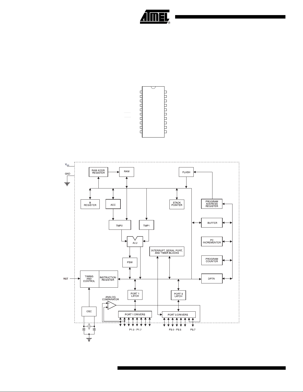
2. Pin Configuration
2.1 20-lead PDIP/SOIC
3. Block Diagram
RST/VPP
(RXD) P3.0
(TXD) P3.1
XTAL2
XTAL1
(INT0) P3.2
(INT1) P3.3
(T0) P3.4
(T1) P3.5
GND
1
2
3
4
5
6
7
8
9
10
20
19
18
17
16
15
14
13
12
11
VCC
P1.7 (SCK)
P1.6 (MISO)
P1.5 (MOSI)
P1.4
P1.3
P1.2
P1.1 (AIN1)
P1.0 (AIN0)
P3.7
2
AT89S2051/S4051
3390D–MICRO–3/07
4. Pin Description
4.1 VCC
Supply voltage.
4.2 GND
Ground.
4.3 Port 1
Port 1 is an 8-bit bi-directional I/O port. Port pins P1.2 to P1.7 provide internal pull-ups. P1.0 and
P1.1 require external pull-ups. P1.0 and P1.1 also serve as the positive input (AIN0) and the
negative input (AIN1), respectively, of the on-chip precision analog comparator. The Port 1 output buffers can sink 20 mA and can drive LED displays directly. When 1s are written to Port 1
pins, they can be used as inputs. When pins P1.2 to P1.7 are used as inputs and are externally
pulled low, they will source current (I
Port 1 also receives code data during Flash programming and verification.
) because of the internal pull-ups.
IL
Port Pin Alternate Functions
AT89S2051/S4051
4.4 Port 3
P1.5 MOSI (Master data output, slave data input pin for ISP channel)
P1.6 MISO (Master data input, slave data output pin for ISP channel)
P1.7 SCK (Master clock output, slave clock input pin for ISP channel)
Port 3 pins P3.0 to P3.5, P3.7 are seven bi-directional I/O pins with internal pull-ups.
P3.6 is hard-wired as an input to the output of the on-chip comparator and is not accessible as a
general-purpose I/O pin. The Port 3 output buffers can sink 20 mA. When 1s are written to Port
3 pins they are pulled high by the internal pull-ups and can be used as inputs. As inputs, Port 3
pins that are externally being pulled low will source current (I
) because of the pull-ups.
IL
Port 3 also serves the functions of various special features of the AT89S2051/S4051 as listed
below:
Port Pin Alternate Functions
P3.0 RXD (serial input port)
P3.1 TXD (serial output port)
P3.2 INT0
P3.3 INT1
P3.4 T0 (timer 0 external input)
(external interrupt 0)
(external interrupt 1)
3390D–MICRO–3/07
P3.5 T1 (timer 1 external input)/ PWM output
Port 3 also receives some control signals for Flash programming and verification.
3
4.5 RST
Reset input. Holding the RST pin high for two machine cycles while the is running resets the
device.
Each machine cycle takes 6 or clock cycles.
4.6 XTAL1
Input to the inverting amplifier and input to the internal clock operating circuit.
4.7 XTAL2
Output from the inverting amplifier.
5. Characteristics
XTAL1 and XTAL2 are the input and output, respectively, of an inverting amplifier which can be
configured for use as an on-chip , as shown in Figure 5-1. Either a quartz crystal or ceramic resonator may be used. To drive the device from an external clock source, XTAL2 should be left
unconnected while XTAL1 is driven as shown in Figure 5-2. There are no requirements on the
duty cycle of the external clock signal, since the input to the internal clocking circuitry is through
a divide-by-two flip-flop, but minimum and maximum voltage high and low time specifications
must be observed.
Figure 5-1. Connections
Note: C1, C2 = 5 pF ± 5 pF for Crystals
= 5 pF ± 5 pF for Ceramic Resonators
Figure 5-2. External Clock Drive Configuration
4
AT89S2051/S4051
3390D–MICRO–3/07
6. X2 Mode Description
The clock for the entire circuit and peripherals is normally divided by 2 before being used by the
CPU core and peripherals. This allows any cyclic ratio (duty cycle) to be accepted on XTAL1
input. In X2 mode this divider is bypassed. Figure 6-1 shows the clock generation block diagram.
Figure 6-1. Clock Generation Block Diagram
XTAL1
X2 Mode
÷
2
AT89S2051/S4051
(XTAL1)/2
F
XTAL
7. Special Function Registers
A map of the on-chip memory area called the Special Function Register (SFR) space is shown in
Table 7-1.
Note that not all of the addresses are occupied, and unoccupied addresses may not be implemented on the chip. Read accesses to these addresses will in general return random data, and
write accesses will have an indeterminate effect.
User software should not write 1s to these unlisted locations, since they may be used in future
products to invoke new features. In that case, the reset or inactive values of the new bits will
always be 0.
F
OSC
State Machine: 6 Clock Cycles
CPU Control
3390D–MICRO–3/07
5

Table 7-1. AT89S2051/S4051 SFR Map and Reset Values
0F8H 0FFH
0F0H
0E8H 0EFH
0E0H
0D8H 0DFH
0D0H
0C8H
0C0H 0C7H
0B8H
0B0H
0A8H
0A0H
B
00000000
ACC
00000000
PSW
00000000
IP
X0X00000
P3
11111111
IE
00X00000
SADEN
00000000
SADDR
00000000
IPH
X0X00000
0F7H
0E7H
0D7H
0CFH
0BFH
0B7H
0AFH
0A7H
98H
90H
88H
80H
SCON
00000000
P1
11111111
TCON
00000000
SBUF
XXXXXXXX
TMOD
00000000
SP
00000111
TL0
00000000
DPL
00000000
TL1
00000000
DPH
00000000
TH0
00000000
TH1
00000000
ACSR
XXX00000
CLKREG
XXXXXX0X
PCON
000X0000
9FH
97H
8FH
87H
6
AT89S2051/S4051
3390D–MICRO–3/07

8. Restrictions on Certain Instructions
The AT89S2051/S4051 is an economical and cost-effective member of Atmel’s family of microcontrollers. It contains 2K/4K bytes of Flash program memory. It is fully compatible with the
MCS-51 architecture, and can be programmed using the MCS-51 instruction set. However,
there are a few considerations one must keep in mind when utilizing certain instructions to program this device.
All the instructions related to jumping or branching should be restricted such that the destination
address falls within the physical program memory space of the device, which is 2K/4K for the
AT89S2051/S4051. This should be the responsibility of the software programmer. For example,
LJMP 7E0H would be a valid instruction for the AT89S2051 (with 2K of memory), whereas LJMP
900H would not.
8.1 Branching Instructions
LCALL, LJMP, ACALL, AJMP, SJMP, JMP @A+DPTR. These unconditional branching
instructions will execute correctly as long as the programmer keeps in mind that the destination
branching address must fall within the physical boundaries of the program memory size (locations 00H to 7FFH/FFFH for the AT89S2051/S4051). Violating the physical space limits may
cause unknown program behavior.
CJNE [...], DJNZ [...], JB, JNB, JC, JNC, JBC, JZ, JNZ. With these conditional branching
instructions, the same rule above applies. Again, violating the memory boundaries may cause
erratic execution.
AT89S2051/S4051
For applications involving interrupts, the normal interrupt service routine address locations of the
80C51 family architecture have been preserved.
8.2 MOVX-related Instructions, Data Memory
The AT89S2051/S4051 contains 256 bytes of internal data memory. External DATA memory
access is not supported in this device, nor is external PROGRAM memory execution. Therefore,
no MOVX [...] instructions should be included in the program.
A typical 80C51 assembler will still assemble instructions, even if they are written in violation of
the restrictions mentioned above. It is the responsibility of the user to know the physical features
and limitations of the device being used and adjust the instructions used accordingly.
9. Program Memory Lock Bits
On the chip are two lock bits which can be left unprogrammed (U) or can be programmed (P) to
obtain the additional features listed in Table 9-1:
Table 9-1. Lock Bit Protection Modes
Program Lock Bits
LB1 LB2 Protection Type
1 U U No program lock features.
2 P U Further programming of the Flash is disabled.
3 P P Same as mode 2, also verify is disabled.
(1)
3390D–MICRO–3/07
Note: 1. The Lock Bits can only be erased with the Chip Erase operation.
7
10. Reset
During reset, all I/O Registers are set to their initial values, the port pins are weakly pulled to
V
, and the program starts execution from the Reset Vector, 0000H. The AT89S2051/S4051
CC
has three sources of reset: power-on reset, brown-out reset, and external reset.
10.1 Power-On Reset
A Power-On Reset (POR) is generated by an on-chip detection circuit. The detection level is
nominally 1.4V. The POR is activated whenever V
cuit can be used to trigger the start-up reset or to detect a supply voltage failure in devices
without a brown-out detector. The POR circuit ensures that the device is reset from power-on.
When V
XTAL Oscillator Bypass fuse is OFF). Only after V
detection) level (see Section 10.2 ”Brown-out Reset”), the BOD delay counter starts measuring a
2-ms delay after which the Internal Reset is deasserted and the microcontroller starts executing.
The built-in 2-ms delay allows the V
ing, thus guaranteeing the maximum operating clock frequency. The POR signal is activated
again, without any delay, when V
a cold reset) will set the POF flag in PCON. Refer to Figure 10-1 for details on the POR/BOD
behavior.
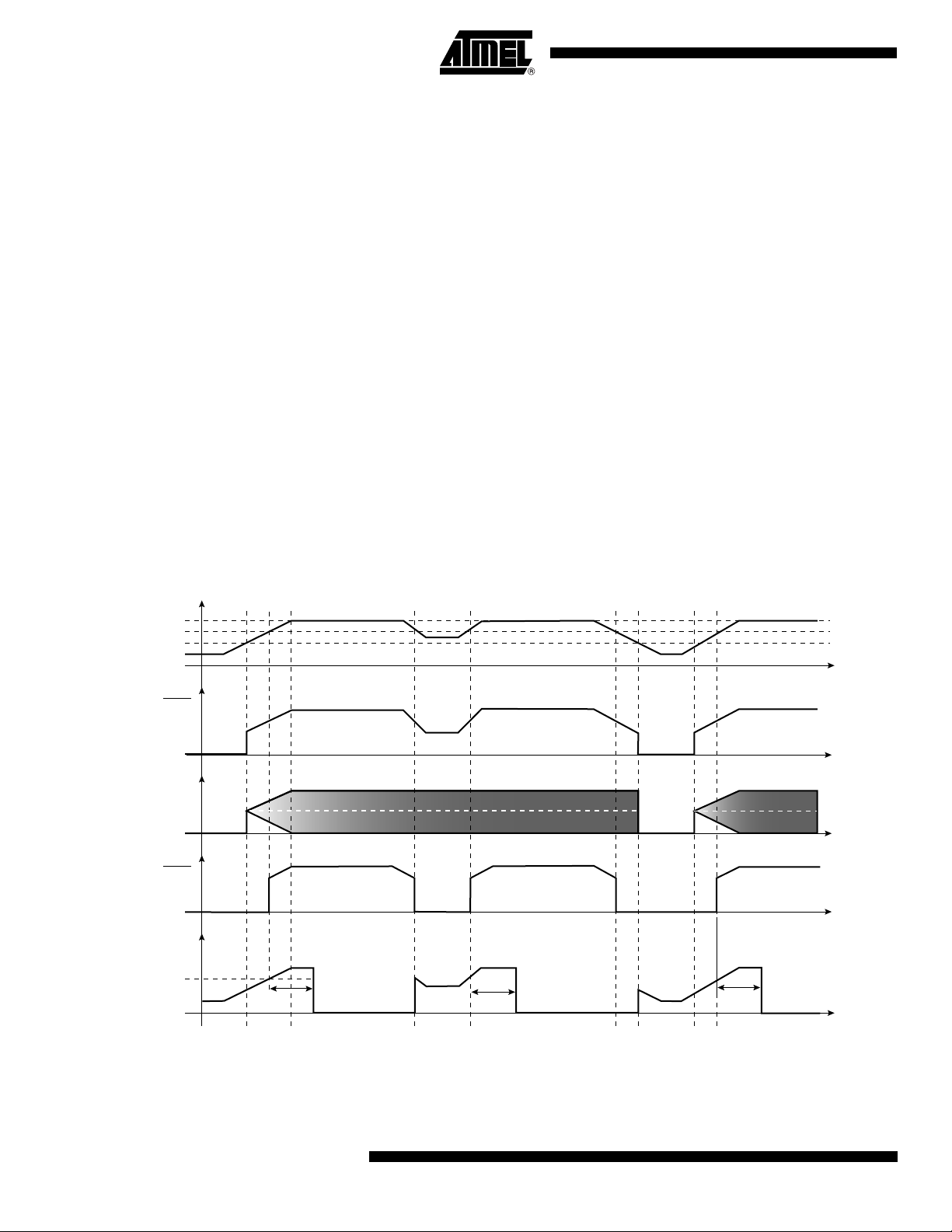
Figure 10-1. Power-up and Brown-out Detection Sequence
reaches the Power-on Reset threshold voltage, the Pierce Oscillator is enabled (if the
CC
is below the detection level. The POR cir-
CC
has also reached the BOD (brown-out
CC
voltage to reach the minimum 2.7V level before execut-
CC
falls below the POR threshold level. A Power-On Reset (i.e.
CC
Level 2.7V
Min V
CC
BOD Level 2.3V
POR Level 1.4V
XTAL1
Internal
RESET
POR
BOD
V
CC
t
t
2.4V
1.2V
t
t
t
POR
(2 ms)
t
POR
(2 ms)
t
POR
(2 ms)
t
0
8
AT89S2051/S4051
3390D–MICRO–3/07

10.2 Brown-out Reset
The AT89S2051/S4051 has an on-chip Brown-out Detection (BOD) circuit for monitoring the V
level during operation by comparing it to a fixed trigger level. The trigger level for the BOD is
nominally 2.0V. The purpose of the BOD is to ensure that if V
speed, the system will gracefully enter reset without the possibility of errors induced by incorrect
execution. When V
diately activated. When V
microcontroller after the timeout period has expired in approximately 2 ms.
10.3 External Reset
The RST pin functions as an active-high reset input. The pin must be held high for at least two
machine cycles to trigger the internal reset. RST also serves as the In-System Programming
(ISP) enable input. ISP mode is enabled when the external reset pin is held high and the ISP
Enable fuse is set.
AT89S2051/S4051
fails or dips while executing at
CC
decreases to a value below the trigger level, the Brown-out Reset is imme-
CC
increases above the trigger level, the BOD delay counter starts the
CC
CC
11. Clock Register
.
Table 11-1.
CLKREG = 8FH Reset Value = XXXX XX0XB
Not Bit Addressable
––––––PWDEXX2
Bit76543210
Symbol Function
PWDEX
X2
CLKREG
Power-down Exit Mode. When PWDEX = 1, wake up from Power-down is externally controlled. When PWDEX = 0, wake
up from Power-down is internally timed.
When X2 = 0, the frequency (at XTAL1 pin) is internally divided by 2 before it is used as the device system frequency.
When X2 = 1, the divide by 2 is no longer used and the XTAL1 frequency becomes the device system frequency. This
enables the user to use a 6 MHz crystal instead of a 12 MHz crystal in order to reduce EMI. The X2 bit is initialized on
power-up with the value of the X2 user fuse and may be changed at runtime by software.
– Clock Register
3390D–MICRO–3/07
9

12. Power Saving Modes
The AT89S2051/S4051 supports two power-reducing modes: Idle and Power-down. These
modes are accessed through the PCON register.
12.1 Idle Mode
Setting the IDL bit in PCON enters idle mode. Idle mode halts the internal CPU clock. The CPU
state is preserved in its entirety, including the RAM, stack pointer, program counter, program
status word, and accumulator. The Port pins hold the logical states they had at the time that Idle
was activated. Idle mode leaves the peripherals running in order to allow them to wake up the
CPU when an interrupt is generated. Timer 0, Timer 1, and the UART will continue to function
during Idle mode. The analog comparator is disabled during Idle. Any enabled interrupt source
or reset may terminate Idle mode. When exiting Idle mode with an interrupt, the interrupt will
immediately be serviced, and following RETI, the next instruction to be executed will be the one
following the instruction that put the device into Idle.
P1.0 and P1.1 should be set to “0” if no external pull-ups are used, or set to “1” if external pullups are used.
12.2 Power-down Mode
Setting the PD bit in PCON enters Power-down mode. Power-down mode stops the and powers
down the Flash memory in order to minimize power consumption. Only the power-on circuitry
will continue to draw power during Power-down. During Power-down the power supply voltage
may be reduced to the RAM keep-alive voltage. The RAM contents will be retained; however,
the SFR contents are not guaranteed once V
by external reset, power-on reset, or certain interrupts.
has been reduced. Power-down may be exited
CC
The user should not attempt to enter (or re-enter) the power-down mode for a minimum of 4 µs
until after one of the following conditions has occurred: Start of code execution (after any type of
reset), or Exit from power-down mode.
12.3 Interrupt Recovery from Power-down
Two external interrupts may be configured to terminate Power-down mode. External interrupts
INT0
(P3.2) and INT1 (P3.3) may be used to exit Power-down. To wake up by external interrupt
INT0
or INT1, the interrupt must be enabled and configured for level-sensitive operation.
When terminating Power-down by an interrupt, two different wake up modes are available.
When PWDEX in CLKREG.2 is zero, the wake up period is internally timed. At the falling edge
on the interrupt pin, Power-down is exited, the is restarted, and an internal timer begins counting. The internal clock will not be allowed to propagate and the CPU will not resume execution
until after the timer has counted for nominally 2 ms. After the timeout period the interrupt service
routine will begin. To prevent the interrupt from re-triggering, the ISR should disable the interrupt
before returning. The interrupt pin should be held low until the device has timed out and begun
executing.
When PWDEX = 1 the wakeup period is controlled externally by the interrupt. Again, at the falling edge on the interrupt pin, Power-down is exited and the is restarted. However, the internal
clock will not propagate and CPU will not resume execution until the rising edge of the interrupt
pin. After the rising edge on the pin, the interrupt service routine will begin. The interrupt should
be held low long enough for the to stabilize.
10
AT89S2051/S4051
3390D–MICRO–3/07
12.4 Reset Recovery from Power-down
Wakeup from Power-down through an external reset is similar to the interrupt with PWDEX = 0.
At the rising edge of RST, Power-down is exited, the is restarted, and an internal timer begins
counting. The internal clock will not be allowed to propagate to the CPU until after the timer has
counted for nominally 2 ms. The RST pin must be held high for longer than the timeout period to
ensure that the device is reset properly. The device will begin executing once RST is brought
low.
It should be noted that when idle is terminated by a hardware reset, the device normally
resumes program execution, from where it left off, up to two machine cycles before the internal
reset algorithm takes control. On-chip hardware inhibits access to internal RAM in this event, but
access to the port pins is not inhibited. To eliminate the possibility of an unexpected write to a
port pin when Idle is terminated by reset, the instruction following the one that invokes Idle
should not be one that writes to a port pin or to external memory.
P1.0 and P1.1 should be set to “0” if no external pull-ups are used, or set to “1” if external pullups are used.
.
AT89S2051/S4051
Table 12-1.
PCON = 87H Reset Value = 000X 0000B
Not Bit Addressable
SMOD1 SMOD0 PWMEN POF GF1 GF0 PD IDL
Bit76543210
Symbol Function
SMOD1 Double Baud Rate bit. Doubles the baud rate of the UART in modes 1, 2, or 3.
SMOD0
PWMEN
POF
GF1, GF0 General-purpose Flags
PD Power Down bit. Setting this bit activates power down operation.
IDL Idle Mode bit. Setting this bit activates idle mode operation
PCON
– Power Control Register
Frame Error Select. When SMOD0 = 0, SCON.7 is SM0. When SMOD0 = 1, SCON.7 is FE. Note that FE will be set after
a frame error regardless of the state of SMOD0.
Pulse Width Modulation Enable. When PWMEN = 1, Timer 0 and Timer 1 are configured as an 8-bit PWM counter with
8-bit auto-reload prescaler. The PWM outputs on T1 (P3.5).
Power Off Flag. POF is set to “1” during power up (i.e. cold reset). It can be set or reset under software control and is not
affected by RST or BOD (i.e. warm resets).
3390D–MICRO–3/07
11

13. Interrupts
The AT89S2051/S4051 provides 6 interrupt sources: two external interrupts, two timer interrupts, a serial port interrupt, and an analog comparator interrupt. These interrupts and the
system reset each have a separate program vector at the start of the program memory space.
Each interrupt source can be individually enabled or disabled by setting or clearing a bit in the
interrupt enable register IE. The IE register also contains a global disable bit, EA, which disables
all interrupts.
Each interrupt source can be individually programmed to one of four priority levels by setting or
clearing bits in the interrupt priority registers IP and IPH. An interrupt service routine in progress
can be interrupted by a higher priority interrupt, but not by another interrupt of the same or lower
priority. The highest priority interrupt cannot be interrupted by any other interrupt source. If two
requests of different priority levels are pending at the end of an instruction, the request of higher
priority level is serviced. If requests of the same priority level are pending at the end of an
instruction, an internal polling sequence determines which request is serviced. The polling
sequence is based on the vector address; an interrupt with a lower vector address has higher
priority than an interrupt with a higher vector address. Note that the polling sequence is only
used to resolve pending requests of the same priority level.
The External Interrupts INT0
depending on bits IT0 and IT1 in Register TCON. The flags that actually generate these interrupts are the IE0 and IE1 bits in TCON. When the service routine is vectored to, hardware clears
the flag that generated an external interrupt only if the interrupt was transition-activated. If the
interrupt was level activated, then the external requesting source (rather than the on-chip hardware) controls the request flag.
The Timer 0 and Timer 1 Interrupts are generated by TF0 and TF1, which are set by a rollover in
their respective Timer/Counter registers (except for Timer 0 in Mode 3). When a timer interrupt is
generated, the on-chip hardware clears the flag that generated it when the service routine is
vectored to.
The Serial Port Interrupt is generated by the logical OR of RI and TI in SCON. Neither of these
flags is cleared by hardware when the service routine is vectored to. In fact, the service routine
normally must determine whether RI or TI generated the interrupt, and the bit must be cleared in
software.
The CF bit in ACSR generates the Comparator Interrupt. The flag is not cleared by hardware
when the service routine is vectored to and must be cleared by software.
Most of the bits that generate interrupts can be set or cleared by software, with the same result
as though they had been set or cleared by hardware. That is, interrupts can be generated and
pending interrupts can be canceled in software.
Interrupt Source Vector Address
System Reset RST or POR or BOD 0000H
and INT1 can each be either level-activated or transition-activated,
12
External Interrupt 0 IE0 0003H
Timer 0 Overflow TF0 000BH
External Interrupt 1 IE1 0013H
Timer 1 Overflow TF1 001BH
Serial Port RI or TI 0023H
Analog Comparator CF 0033H
AT89S2051/S4051
3390D–MICRO–3/07
14. Interrupt Registers
AT89S2051/S4051
Table 14-1.
IE = A8H Reset Value = 00X0 0000B
Bit Addressable
EA EC – ES ET1 EX1 ET0 EX0
Bit76543210
Symbol Function
EA
EC Comparator Interrupt Enable
ES Serial Port Interrupt Enable
ET1 Timer 1 Interrupt Enable
EX1 External Interrupt 1 Enable
ET0 Timer 0 Interrupt Enable
EX0 External Interrupt 0 Enable
Table 14-2.
IP = B8H Reset Value = X0X0 0000B
Bit Addressable
– PC – PS PT1 PX1 PT0 PX0
Bit76543210
IE
– Interrupt Enable Register
Global enable/disable. All interrupts are disabled when EA = 0. When EA = 1, each interrupt source is enabled/disabled
by setting/clearing its own enable bit.
.
IP
– Interrupt Priority Register
Symbol Function
PC Comparator Interrupt Priority Low
PS Serial Port Interrupt Priority Low
PT1 Timer 1 Interrupt Priority Low
PX1 External Interrupt 1 Priority Low
PT0 Timer 0 Interrupt Priority Low
PX0 External Interrupt 0 Priority Low
Table 14-3.
IPH = B7H Reset Value = X0X0 0000B
Not Bit Addressable
– PCH – PSH PT1H PX1H PT0H PX0H
Bit76543210
Symbol Function
PCH Comparator Interrupt Priority High
PSH Serial Port Interrupt Priority High
PT1H Timer 1 Interrupt Priority High
PX1H External Interrupt 1 Priority High
PT0H Timer 0 Interrupt Priority High
PX0H External Interrupt 0 Priority High
IPH
– Interrupt Priority High Register
.
3390D–MICRO–3/07
13
15. Timer/Counters
C
The AT89S2051/S4051 have two 16-bit Timer/Counters: Timer 0 and Timer 1. The
Timer/Counters are identical to those in the AT89C2051/C4051. For more detailed information
on the Timer/Counter operation, please click on the document link below:
http://www.atmel.com/dyn/resources/prod_documents/DOC4316.PDF
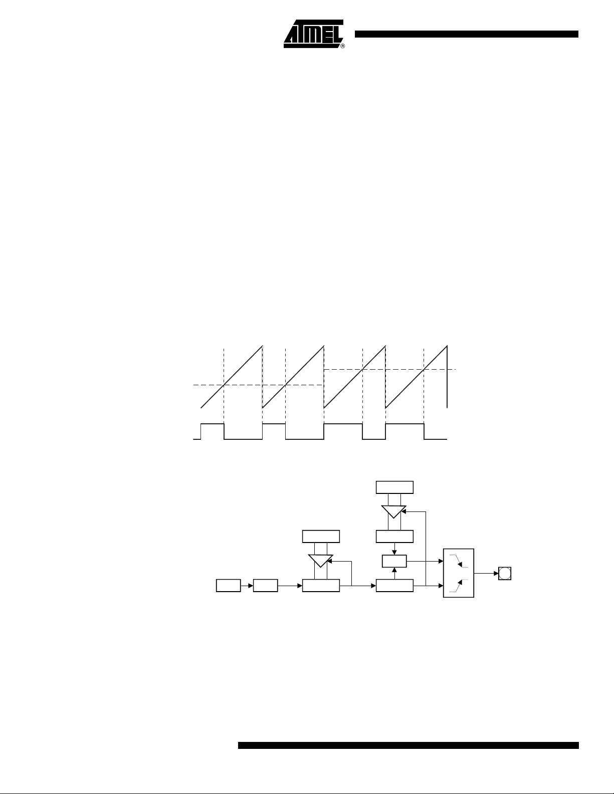
16. Pulse Width Modulation
Timer 0 and Timer 1 may be configured as an 8-bit pulse width modulator by setting the PWMEN
bit in PCON. The generated waveform is output on the Timer 1 input pin, T1. In PWM mode
Timer 0 acts as an 8-bit prescaler to select the PWM timebase. Timer 0 is forced into Mode 2 (8bit auto-reload) by PWMEN and the value in TH0 will determine the clock division from 0 (FFh)
to 256 (00h). Timer 1 acts as the 8-bit PWM counter. TL1 counts once on every overflow from
TL0. TH1 stores the 8-bit pulse width value. On the FFh-->00h overflow of TL1, the PWM output
is set high. When the count in TL1 matches the value in TH1, the PWM output is set low. Therefore, the output pulse width is proportional to the value in TH1. To prevent glitches, writes to TH1
only take effect on the FFh-->00h overflow of TL1. However, a read from TH1 will read the new
value at any time after a write to TH1. See Figure 16-1 for PWM waveform example.
Figure 16-1. Pulse Width Modulation (PWM) Output Waveform
Counter Value (TL1)
Compare Value (TH1)
PWM Output (T1)
Figure 16-2. Timer 0/1 Pulse Width Modulation Mode
TH1
TH0
S
O
12
÷÷
T
L0
OCR
=
T
L1
P3.
?
PWM
5
TL0 counts once every machine cycle (1 machine cycle = 12 clocks in X1 mode) and TH0 is the
reload value for when TL0 overflows. Every time TL0 overflows TL1 increments by one, with TL0
overflowing after counting 256 minus TH0 machine cycles.
To calculate the pulse width for the PWM output on pin T1, users should use the following
formula:
TH1 * (256 - TH0) * (1/clock_freq) * 12 = Pulse Width
14
AT89S2051/S4051
3390D–MICRO–3/07

AT89S2051/S4051
T
TL1 will always count from 00h to FFh. The output on the Timer 1 (T1) pin will be high from when
TL1 equals 00h until TL1 equals TH1 (see Figure 16-3). TH1 does not act as the reload value for
TL1 on overflow. Instead, TH1 is used strictly as a compare value (see Figure 16-2).
Figure 16-3. Example of a PWM Output
17. UART
The UART in the AT89S2051/S4051 operates the same way as the UART in the
AT89C2051/C4051. For more detailed information on the UART operation, please click on the
document link below:
17.1 Enhanced UART
In addition to all of its usual modes, the UART can perform framing error detection by looking for
missing stop bits, and automatic address recognition. The UART also fully supports multiprocessor communication as does the standard 80C51 UART.
When used for framing error detect, the UART looks for missing stop bits in the communication.
A missing bit will set the FE bit in the SCON register. The FE bit shares the SCON.7 bit with SM0
and the function of SCON.7 is determined by PCON.6 (SMOD0). If SMOD0 is set then SCON.7
functions as FE. SCON.7 functions as SM0 when SMOD0 is cleared. When used as FE,
SCON.7 can only be cleared by software.
L1 Count
00 01 10 . . . TH1 . . . FF 00 . . .
T1
http://www.atmel.com/dyn/resources/prod_documents/DOC4316.PDF
17.2 Automatic Address Recognition
Automatic Address Recognition is a feature which allows the UART to recognize certain
addresses in the serial bit stream by using hardware to make the comparisons. This feature
saves a great deal of software overhead by eliminating the need for the software to examine
every serial address which passes by the serial port. This feature is enabled by setting the SM2
bit in SCON. In the 9-bit UART modes, mode 2 and mode 3, the Receive Interrupt flag (RI) will
be automatically set when the received byte contains either the “Given” address or the “Broadcast” address. The 9-bit mode requires that the 9th information bit is a 1 to indicate that the
received information is an address and not data.
The 8-bit mode is called mode 1. In this mode the RI flag will be set if SM2 is enabled and the
information received has a valid stop bit following the 8 address bits and the information is either
a Given or Broadcast address.
Mode 0 is the Shift Register mode and SM2 is ignored.
Using the Automatic Address Recognition feature allows a master to selectively communicate
with one or more slaves by invoking the given slave address or addresses. All of the slaves may
be contacted by using the Broadcast address. Two special Function Registers are used to
define the slave’s address, SADDR, and the address mask, SADEN. SADEN is used to define
which bits in the SADDR are to be used and which bits are “don’t care”. The SADEN mask can
3390D–MICRO–3/07
15

be logically ANDed with the SADDR to create the “Given” address which the master will use for
addressing each of the slaves. Use of the Given address allows multiple slaves to be recognized
while excluding others. The following examples will help to show the versatility of this scheme:
Slave 0 SADDR = 1100 0000
SADEN = 1111 1101
Given = 1100 00X0
Slave 1 SADDR = 1100 0000
SADEN = 1111 1110
Given = 1100 000X
In the previous example SADDR is the same and the SADEN data is used to differentiate
between the two slaves. Slave 0 requires a 0 in bit 0 and it ignores bit 1. Slave 1 requires a 0 in
bit 1 and bit 0 is ignored. A unique address for slave 0 would be 1100 0010 since slave 1
requires a 0 in bit 1. A unique address for slave 1 would be 1100 0001 since a 1 in bit 0 will
exclude slave 0. Both slaves can be selected at the same time by an address which has bit 0 = 0
(for slave 0) and bit 1 = 0 (for slave 1). Thus, both could be addressed with 1100 0000.
In a more complex system the following could be used to select slaves 1 and 2 while excluding
slave 0:
Slave 0 SADDR = 1100 0000
SADEN = 1111 1001
Given = 1100 0XX0
Slave 1 SADDR = 1110 0000
SADEN = 1111 1010
Given = 1110 0X0X
Slave 2 SADDR = 1110 0000
SADEN = 1111 1100
Given = 1110 00XX
In the above example the differentiation among the 3 slaves is in the lower 3 address bits. Slave
0 requires that bit 0 = 0 and it can be uniquely addressed by 1110 0110. Slave 1 requires that bit
1 = 0 and it can be uniquely addressed by 1110 and 0101. Slave 2 requires that bit 2 = 0 and its
unique address is 1110 0011. To select Slaves 0 and 1 and exclude Slave 2, use address 1110
0100, since it is necessary to make bit 2 = 1 to exclude slave 2.
The Broadcast Address for each slave is created by taking the logical OR of SADDR and
SADEN. Zeros in this result are trended as don’t cares. In most cases, interpreting the don’t
cares as ones, the broadcast address will be FF hexadecimal.
16
Upon reset SADDR (SFR address 0A9H) and SADEN (SFR address 0B9H) are loaded with 0s.
This produces a given address of all “don’t cares” as well as a Broadcast address of all “don’t
cares”. This effectively disables the Automatic Addressing mode and allows the microcontroller
to use standard 80C51-type UART drivers which do not make use of this feature.
AT89S2051/S4051
3390D–MICRO–3/07

AT89S2051/S4051
Table 17-1. SCON – Serial Port Control Register
SCON Address = 98H Reset Value = 0000 0000B
Bit Addressable
SM0/FE SM1 SM2 REN TB8 RB8 TI RI
Bit7 6543210
(SMOD = 0/1)
Symbol Function
Framing error bit. This bit is set by the receiver when an invalid stop bit is detected. The FE bit is not cleared by valid
FE
SM0 Serial Port Mode Bit 0, (SMOD must = 0 to access bit SM0)
SM1
frames but should be cleared by software. The SMOD0 bit must be set to enable access to the FE bit. FE will be set
regardless of the state of SMOD.
Serial Port Mode Bit 1
(1)
SM0 SM1 Mode Description Baud Rate
0 0 0 shift register f
0 1 1 8-bit UART variable
1 0 2 9-bit UART f
1 1 3 9-bit UART variable
/64 or f
osc
osc
/12
osc
(2)
/32
Enables the Automatic Address Recognition feature in modes 2 or 3. If SM2 = 1 then Rl will not be set unless the received
SM2
REN
TB8
RB8
TI
RI
Notes: 1. SMOD is located at PCON.7.
9th data bit (RB8) is 1, indicating an address, and the received byte is a Given or Broadcast Address. In mode 1, if SM2 =
1 then Rl will not be activated unless a valid stop bit was received, and the received byte is a Given or Broadcast Address.
In Mode 0, SM2 should be 0.
Enables serial reception. Set by software to enable reception. Clear by software to disable reception.
The 9th data bit that will be transmitted in modes 2 and 3. Set or clear by software as desired.
In modes 2 and 3, the 9th data bit that was received. In mode 1, if SM2 = 0, RB8 is the stop bit that was
received. In mode 0, RB8 is not used.
Transmit interrupt flag. Set by hardware at the end of the 8th bit time in mode 0, or at the beginning of the
stop bit in the other modes, in any serial transmission. Must be cleared by software.
Receive interrupt flag. Set by hardware at the end of the 8th bit time in mode 0, or halfway through the stop
bit time in the other modes, in any serial reception (except see SM2). Must be cleared by software.
= frequency.
2. f
osc
3390D–MICRO–3/07
17

18. Analog Comparator
A single analog comparator is provided in the AT89S2051/S4051. The comparator operation is
such that the output is a logical “1” when the positive input AIN0 (P1.0]) is greater than the negative input AIN1 (P1.1). Otherwise the output is a zero. Setting the CEN bit in ACSR enables the
comparator. When the comparator is first enabled, the comparator output and interrupt flag are
not guaranteed to be stable for 10 microseconds. The corresponding comparator interrupt
should not be enabled during that time, and the comparator interrupt flag must be cleared before
the interrupt is enabled in order to prevent an immediate interrupt service.
The comparator may be configured to cause an interrupt under a variety of output value conditions by setting the CM bits in ACSR. The comparator interrupt flag CF in ACSR is set whenever
the comparator output matches the condition specified by CM. The flag may be polled by software or may be used to generate an interrupt and must be cleared by software. The analog
comparator is always disabled during Idle or Power-down modes.
19. Comparator Interrupt with Debouncing
The comparator output is sampled at every State 4 (S4) of every machine cycle. The conditions
on the analog inputs may be such that the comparator output will toggle excessively. This is
especially true if applying slow moving analog inputs. Three debouncing modes are provided to
filter out this noise. In debouncing mode, the comparator uses Timer 1 to modulate its sampling
time. When a relevant transition occurs, the comparator waits until two Timer 1 overflows have
occurred before resampling the output. If the new sample agrees with the expected value, CF is
set. Otherwise, the event is ignored. The filter may be tuned by adjusting the timeout period of
Timer 1. Because Timer 1 is free running, the debouncer must wait for two overflows to guarantee that the sampling delay is at least 1 timeout period. Therefore after the initial edge event, the
interrupt may occur between 1 and 2 timeout periods later. See Figure 19-1.
Figure 19-1. Example of Negative Edge Comparator Interrupt with Debouncing
Comparator Out
Timer 1 Overflow
CF
START COMPARE
START COMPARE
18
AT89S2051/S4051
3390D–MICRO–3/07

AT89S2051/S4051
20. Analog Comparator Register
.
Table 20-1.
ACSR = 97H Reset Value = XXX0 0000B
Not Bit Addressable
– – – CF CEN CM2 CM1 CM0
Bit76543210
Symbol Function
CF
CEN
CM [2:0]
ACSR
– Analog Comparator Control & Status Register
Comparator Interrupt Flag. Set when the comparator output meets the conditions specified by the CM [2:0] bits and CEN
is set. The flag must be cleared by software. The interrupt may be enabled/disabled by setting/clearing bit 6 of IE.
Comparator Enable. Set this bit to enable the comparator. Clearing this bit will force the comparator output low and
prevent further events from setting CF.
Comparator Interrupt Mode
2 1 0 Interrupt Mode
--- ---- ---- --------------------------------------0 0 0 Negative (Low) level
001 Positive edge
0 1 0 Toggle with debounce
0 1 1 Positive edge with debounce
100 Negative edge
101 Toggle
1 1 0 Negative edge with debounce
1 1 1 Positive (High) level
3390D–MICRO–3/07
19

21. Parallel Programming Specification
Atmel’s AT89S2051/S4051 offers 2K/4K bytes of In-System Programmable Flash code memory.
In addition, the device contains a 32-byte User Signature Row and a 32-byte read-only Atmel
Signature Row.
Table 21-1. Memory Organization
Device # Page Size # Pages Address Range Page Range
AT89S2051 32 bytes 64 0000H - 07FFH 00H - 3FH
AT89S4051 32 bytes 128 0000H - 0FFFH 00H - 7FH
Figure 21-1. Flash Parallel Programming Device Connections
AT89S2051/S4051
V
RDY/BSY
Note: 1. Sampling of pin P3.1 (RDY/BSY) is optional. In Parallel Mode, P3.1 will be pulled low while the
device is busy. However, it requires an external passive pull-up to VCC. Also, note that P3.6
does not exist, so TestCode connects to P3.7, P3.5, P3.4, and P3.3.
(1)
PROG
TestCode
INC
P3.1
P3.2
P3.7-3
XTAL1
GND
P1.7 - P1.0
RST
CC
2.7V to 5.5V
DATA IN/OUT
V
PP
20
AT89S2051/S4051
3390D–MICRO–3/07

Table 21-2. Parallel Programming Mode Command Summary
Test Control Test Selects Data I/O
AT89S2051/S4051
Mode
Chip Erase
Load X-Address
Page Write
Page Read
Page Write
Page Read
(5)
(2)
(3)(4)(6)
(3)
(3)(4)(6)(7)
(3)(8)(10)
Write Fuse/Lock Bit
Read Fuse/Lock Bit
(5)(9)
(9)
P3.2
(1)
RST
1.0 µs 12V L H L L L XX
H 12V 0.1 µs H L H H D
Code Memory 1.0 µs 12V 0.1 µs L H H H D
Code Memory H 12V 0.1 µs L L H H D
Sig. Row 1.0 µs 12V 0.1 µs L L L L D
Sig. Row H 12V 0.1 µs L L L H D
1.0 µs12V L HHHHD
H12VL HHLLD
INC
P3.3 P3.4 P3.5 P3.7 P1.7-0
Notes: 1. The internal Y-address counter is reset to 00H on the rising/falling edge of RST.
2. A positive pulse on XTAL1 loads the address data on Port P1 into the X-address (page) register and resets the Y-address.
3. A positive pulse on XTAL1 advances the Y-address counter.
4. A low pulse on P3.2 loads data from Port P1 for the current address. If another P3.2 low pulse does not arrive within 150 µs,
programming starts.
5. Internally timed for 4 ms.
6. Internally timed for 2 ms.
7. 00H must be loaded into the X-address before executing this command.
8. Will read User Signature if X-address is 00H, will read Atmel Signature if X-address is 01H.
Fuse/Lock Bit Definitions:
9.
IN
IN
OUT
IN
OUT
IN
OUT
Bit 7
XTAL Osc Bypass
Bit 6
User Row Programming
Bit 5
x2 Clock
Bit 4
Serial Programming
Bit 1
Lock Bit 2
Bit 0
Lock Bit 1
10. Atmel Signature Bytes:
AT89S2051: Address 00H = 1EH
AT89S4051: Address 00H = 1EH
Enable = 0/Disable = 1
Enable = 0/Disable = 1
Enable = 0/Disable = 1
Enable = 0/Disable = 1
Locked = 0/Unlocked = 1
Locked = 0/Unlocked = 1
01H = 23H
02H = FFH
01H = 43H
02H = FFH
3390D–MICRO–3/07
21

22. Power-up Sequence
Execute the following sequence to power-up the device before programming.
1. Apply power between VCC and GND pins.
2. After V
3. Wait 4 ms for the internal Power-on Reset to timeout.
4. Bring P3.2 to “H” and drive P3.7, P3.5, P3.4, and P3.3 to known values, then wait
10 µs.
5. Raise RST/V
6. After V
Figure 22-1. Power-up Operation
has settled, wait 10 µs and bring RST to “H”.
CC
to 12V to enable the parallel programming modes.
PP
has settled, wait an additional 10 µs before programming.
PP
V
CC
RST/V
PP
P3.2
XTAL1
P3.3 - P3.7
P1.0 - P1.7
RDY/BSY
23. Power-down Sequence
Execute the following sequence to power-down the device after programming.
1. Tri-state Port P1.
2. Bring RST/V
3. Bring XTAL and P3.2 to “L” and tri-state P3.7, P3.5, P3.4, and P3.3.
4. Bring RST to “L” and wait 10 µs.
5. Power off V
Figure 23-1. Power-down Operation
RST/V
High Z
High Z
High Z
down from 12V to VCC and wait 10 µs.
PP
.
CC
V
CC
PP
P3.2
22
XTAL1
P3.3 - P3.7
P1.0 - P1.7
RDY/BSY
AT89S2051/S4051
High Z
High Z
High Z
3390D–MICRO–3/07

24. Chip Erase
AT89S2051/S4051
Function:
1. FFH programmed to every address location.
2. FFH programmed to User Signature Row if User Row Fuse bit is enabled.
3. Lockbit1 and Lockbit2 programmed to “unlock” state.
Usage:
1. Apply “0001” TestCode to P3.7, P3.5, P3.4, P3.3.
2. Pulse P3.2 low for 1 µs.
3. Wait 4 ms, monitor P3.1, or poll data.
Note: This and the following waveforms are not to scale.
Figure 24-1. Chip Erase Sequence
P3.2
XTAL1
25. Load X-Address
Function:
1. Loads the X-Address register with data on Port P1. The loaded address will select the
2. Resets the Y-Address counter to 00H. The Y-Address is equivalent to bits [4:0] of the
Usage:
1. Apply “1101” TestCode to P3.7, P3.5, P3.4, P3.3.
2. Drive Port P1 with 8-bit X-address data.
3. Pulse XTAL1 high for at least 100 ns. The address is latched on the falling edge of
Figure 25-1. Load X-Address Sequence
P3.3 - P3.7
P1.0 - P1.7
RDY/BSY
High Z
0001
page for subsequent write/read commands. The X-Address is equivalent to bits [11:5]
of the full byte address.
full byte address and selects a byte within a page.
XTAL1.
P3.2
3390D–MICRO–3/07
XTAL1
P3.3 - P3.7
P1.0 - P1.7
RDY/BSY
1101
High Z High Z
XADDR
23

26. Page Write 4K Code
Function:
1. Programs 1 page (1 to 32 bytes) of data into the Code Memory array.
2. X-address (page) determined by previous Load-X command.
3. Y-address (offset) incremented by positive pulse on XTAL1.
4. 1 byte of data is loaded from Port P1 for the current X- and Y-address by a low pulse on
P3.2.
Usage:
1. Execute the Load-X command to set the page address and reset the offset.
2. Apply “1110” TestCode to P3.7, P3.5, P3.4, P3.3.
3. Drive Port P1 with 8-bit data.
4. Pulse P3.2 low for 1 µs to load the data from Port P1.
5. For additional bytes (up to 32), pulse XTAL1 high for at least 100 ns to increment the
Y-address and repeat steps 3 and 4 within 150 µs.
6. Wait 2 ms, monitor P3.1, or poll data.
Note: It is possible to skip bytes by pulsing XTAL1 high multiple times before pulsing P3.2 low.
Figure 26-1. Page Write 4K Code Programming Sequence
P3.2
XTAL1
P3.3 - P3.7
P1.0 - P1.7
RDY/BSY
1101 1110
XADDR
DIN0 DIN1
DIN N-1
High Z
24
AT89S2051/S4051
3390D–MICRO–3/07

27. Read 4K Code
AT89S2051/S4051
Function:
1. Read 1 page (1 to 32 bytes) of data from the Code Memory array.
2. X-address (page) determined by previous Load-X command.
3. Y-address (offset) incremented by positive pulse on XTAL1.
Usage:
1. Execute the Load-X command to set the page address and reset the offset.
2. Apply “1100” TestCode to P3.7, P3.5, P3.4, P3.3.
3. Read 8-bit data on Port P1.
4. For additional bytes (up to 32), pulse XTAL1 high for at least 100 ns to increment the
Y-address and repeat step 3. The address will change on the falling edge of XTAL1.
Figure 27-1. Read 4K Code Programming Sequence
P3.2
XTAL1
P3.3 - P3.7
P1.0 - P1.7
RDY/BSY
1101 1100
XADDR
DOUT0 DOUT1
DOUT N-1
3390D–MICRO–3/07
25

28. Page Write User Signature Row
Function:
1. Programs 1 to 32 bytes of data into the User Signature Row.
2. X-address (page) should be 00H from a previous Load-X command.
3. Y-address (offset) incremented by positive pulse on XTAL1.
4. 1 byte of data is loaded from Port P1 for the current Y-address by a low pulse on P3.2.
5. Disabled if User Row Fuse bit is disabled.
Usage:
1. Execute the Load-X command to set the page to 00H and reset the offset.
2. Apply “0000” TestCode to P3.7, P3.5, P3.4, P3.3.
3. Drive Port P1 with 8-bit data.
4. Pulse P3.2 low for 1 µs to load the data from Port P1.
5. For additional bytes (up to 32), pulse XTAL1 high for at least 100 ns to increment the Yaddress and repeat steps 3 and 4 within 150 µs.
6. Wait 2 ms, monitor P3.1, or poll data.
Note: It is possible to skip bytes by pulsing XTAL1 high multiple times before pulsing P3.2 low.
Figure 28-1. Page Write User Signature Row Sequence
P3.2
XTAL1
P3.3 - P3.7
P1.0 - P1.7
RDY/BSY
1101 0000
00H
DIN0 DIN1
DIN N-1
26
AT89S2051/S4051
3390D–MICRO–3/07

29. Read User Signature Row
Function:
1. Reads 1 to 32 bytes of data from the User Signature Row.
2. X-address (page) should be 00H from a previous Load-X command.
3. Y-address (offset) incremented by positive pulse on XTAL1.
Usage:
1. Execute the Load-X command to set the page to 00H and reset the offset.
2. Apply “1000” TestCode to P3.7, P3.5, P3.4, P3.3.
3. Read 8-bit data on Port P1.
4. For additional bytes (up to 32), pulse XTAL1 high for at least 100 ns to increment the Yaddress and repeat step 3. The address will change on the falling edge of XTAL1.
Figure 29-1. Read User Signature Row Sequence
P3.2
XTAL1
AT89S2051/S4051
P3.3 - P3.7
P1.0 - P1.7
RDY/BSY
1101 1000
00H
DOUT0 DOUT1
DOUT N-1
3390D–MICRO–3/07
27

30. Read Atmel Signature Row
Function:
1. Reads 1 to 32 bytes of data from the Atmel Signature Row.
2. X-address (page) should be 01H from a previous Load-X command.
3. Y-address (offset) incremented by positive pulse on XTAL1.
Usage:
1. Execute the Load-X command to set the page to 01H and reset the offset.
2. Apply “1000” TestCode to P3.7, P3.5, P3.4, P3.3.
3. Read 8-bit data on Port P1.
4. For additional bytes (up to 32), pulse XTAL1 high for at least 100 ns to increment the Yaddress and repeat step 3. The address will change on the falling edge of XTAL1.
Figure 30-1. Read Atmel Signature Row Sequence
P3.2
XTAL1
P3.3 - P3.7
P1.0 - P1.7
RDY/BSY
1101 1000
01H
DOUT0 DOUT1
DOUT N-1
28
AT89S2051/S4051
3390D–MICRO–3/07

31. Write Lock Bits/User Fuses
Function:
1. Program Lock Bits 1 and 2.
2. Program user fuses.
Usage:
1) Apply “1111” TestCode to P3.7, P3.5, P3.4, P3.3.
3. Drive Port P1 with fuse data, bits [7:4] for fuses and bits [1:0] for lock bits.
4. Pulse P3.2 low for 1 µs.
5. Wait 4 ms, monitor P3.1, or poll data.
Figure 31-1. Write Lock Bits/User Fuses
P3.2
XTAL1
AT89S2051/S4051
P3.3 - P3.7
P1.0 - P1.7
RDY/BSY
32. Read Lock Bits/User Fuses
Function:
1. Read status of Lock Bits 1 and 2.
2. Read status of user fuses.
Usage:
1. Apply “0011” TestCode to P3.7, P3.5, P3.4, P3.3.
2. Read fuse data from Port P1, bits [7:4] for fuses and bits [1:0] for lock bits.
Figure 32-1. Read Lock Bits/User Fuses
P3.2
XTAL1
High Z
1111
DATA
High Z
3390D–MICRO–3/07
P3.3. - P3.7
P1.0 - P1.7
RDY/BSY
High Z
0011
DOUT
High Z
29

Figure 32-2. Flash Programming and Verification Waveforms in Parallel Mode
(RDY/BSY)
XTAL1
P3.1
PORT0
P3.3...P3.7
P3.2/PROG
t
POR
RST/VPP
t
PWRUP
VCC
t
PHBL
t
WC
t
XTW
t
ASTP
t
AHLD
t
XLP
t
PHX
t
MSTP
t
PSTP
t
DSTP
t
DHLD
LOADX
MSTP
PAGE WRITE LOADX PAGE READ
t
t
PGW
t
BLT
XADDR DATA0 DATA1 DATAN XADDR DATA0 DATA1 DATAN
t
HSTL
30
t
RDT
AT89S2051/S4051
t
MHLD
t
VFY
t
HSTL
t
PWRDN
3390D–MICRO–3/07

AT89S2051/S4051
Table 32-1. Parallel Flash Programming and Verification Parameters
Symbol Parameter
V
PP
I
PP
t
PWRUP
t
POR
t
PSTP
t
HSTL
t
MSTP
t
MHLD
t
XTW
t
ASTP
t
AHLD
t
PGW
t
DSTP
t
DHLD
t
XLP
t
PHX
t
BLT
t
PHBL
t
WC
t
RDT
t
VFY
t
PWRDN
Programming Enable Voltage 11.5 12.5 V
Programming Enable Current 1.0 mA
Power-on to RST High 10 µs
Power-on Reset Time 2 ms
PROG Setup to VPP High 10 µs
High Voltage Setting time 10 µs
Mode Setup to PROG or XTAL1 1 µs
Mode Hold after PROG or XTAL2 1 µs
XTAL1 High Width 0.5 µs
Address Setup to XTAL1 High 0.5 µs
Address Hold after XTAL1 Low 0.5 µs
PROG Low Width 1 µs
Data Setup to PROG Low 0.5 µs
Data Hold after PROG High 0.5 µs
XTAL1 Low to PROG Low 0.5 µs
PROG High to XTAL1 High 0.5 µs
Byte Load Period 150 µs
PROG High to BUSY Low 256 µs
Wire Cycle Time 4.5 ms
Read Byte Time 1 µs
XTAL1 Low to Data Verify Valid 0.25 µs
RST Low to Power Off 1 µs
Min Max Units
3390D–MICRO–3/07
31

33. In-System Programming (ISP) Specification
Atmel’s AT89S2051/S4051 offers 2K/4K bytes of In-System Programmable Flash code memory.
In addition, the device contains a 32-byte User Signature Row and a 32-byte read-only Atmel
Signature Row.
Table 33-1. Memory Organization
Device # Page Size # Pages Address Range Page Range
AT89S2051 32 bytes 64 0000H - 07FFH 00H - 3FH
AT89S4051 32 bytes 128 0000H - 0FFFH 00H - 7FH
Figure 33-1. ISP Programming Device Connections
AT89S2051/S4051
V
CC
(1)
SCK
SERIAL IN
(MOSI)
Note: 1. SCK frequency should be less than (XTAL frequency)/8.
P1.7
P1.5
XTAL1
GND
P1.6
RST
2.7V to 5.5V
SERIAL OUT
(MISO)
V
CC
32
AT89S2051/S4051
3390D–MICRO–3/07

AT89S2051/S4051
34. Serial Programming Command Summary
Command Byte 1 Byte 2 Byte 3 Byte 4 Byte ...
Program Enable
Chip Erase 1010 1100 100x xxxx xxxx xxxx xxxx xxxx
Write Code Byte 0100 0000
(1)
1010 1100 0101 0011 xxxx xxxx xxxx xxxx
xxxx
A11
A10
A9
A8
A7
A6
A5
A4
A3
A2
A1
A0
D7
D6
D5
D4
D3
D2
D1
D0
Read Code Byte 0010 0000
Write Code Page
Read Code Page
Write User Fuses
Read User Fuses
Write Lock Bits
Read Lock Bits
(4)
(4)
(2)
(2)
(3)
(3)
0101 0000
0011 0000
1010 1100
0010 0001 xxxx xxxx xxxx xxxx
1010 1100
0010 0100 xxxx xxxx xxxx xxxx
xxxx
A11
A10
xxxx
A11
A10
xxxx
A11
A10
0001 xxxx xxxx xxxx xxxx
1110 0x
F3
F2
LB2
Write User Signature Byte 0100 0010 xxxx xxxx
Read User Signature Byte 0010 0010 xxxx xxxx
Write User Signature Page
Read User Signature Page
Read Atmel Signature Byte
(2)
(2)
(5)
0101 0010 xxxx xxxx xxxx xxxx Data 0 ... Data 31
0011 0010 xxxx xxxx xxxx xxxx Data 0 ... Data 31
0010 1000 xxxx xxxx xxx
A9
A9
A9
F1
A8
A8
A8
F0
LB1
A6
A7
0 0000 Data 0 ... Data 31
A7
A6
A5
0 0000 Data 0 ... Data 31
A7
A6
A5
A4
A0
xxxx
D7
D6
D5
F3
D4
F2
F1
D3
F0
D2
D1
D0
A1
A5
A3
A2
xxxx xxxx xxxx xxxx
xxxx xx
LB1
LB2
xxx
xxx
A4
A4
A4
A3
A3
A3
A2
A2
A2
A1
A1
A1
A0
A0
A0
D7
D7
D7
D6
D6
D6
D5
D5
D5
D4
D4
D4
D3
D3
D3
D2
D2
D2
D1
D1
D1
D0
D0
D0
Notes: 1. Program Enable must be the first command issued after entering into the serial programming mode.
2. All 32 Data bytes must be written/read.
3. Fuse Bit Definitions:
Bit 0
ISP Enable*
Bit 1
x2 Clock
Bit 2
User Row Programming
Bit 3
XTAL Osc Bypass**
Enable = 0/Disable = 1
Enable = 0/Disable = 1
Enable = 0/Disable = 1
Enable = 0/Disable = 1
*The ISP Enable Fuse must be enabled before entering ISP mode.
When disabling the ISP fuse during ISP mode, the current fuse state will remain active until RST is brought low.
**Any change will only take effect after the next power-down/power-up cycle event.
4. Lock Bit Definitions:
Bit 0
Bit 1
Lock Bit 1
Lock Bit 2
Locked = 0/Unlocked = 1
Locked = 0/Unlocked = 1
5. Atmel Signature Bytes:
AT89S2051: Address 00H = 1EH
01H = 23H
02H = FFH
AT89S4051: Address 00H = 1EH
01H = 43H
02H = FFH
3390D–MICRO–3/07
33

35. Power-up Sequence
Execute this sequence to power-up the device before programming.
1. Apply power between VCC and GND pins.
2. Keep SCK (P1.7) at GND.
3. Wait 10 µs and bring RST to “H”.
4. If a crystal is connected between XTAL1 and XTAL2, wait at least 10 ms; otherwise,
apply a 3 - 24 MHz clock to XTAL1 and wait 4 ms.
Figure 35-1. ISP Power-up Sequence
P1.7/SCK
V
CC
RST
XTAL1
P1.6/MISO
P1.5/MOSI
36. ISP Start Sequence
Execute this sequence to enter ISP when the device is already operational.
1. Bring SCK (P1.7) to GND.
2. Tri-state MISO (P1.6).
3. Bring RST to “H”.
Figure 36-1. ISP Start Sequence
P1.7/SCK
V
CC
RST
XTAL1
High Z
34
P1.6/MISO
P1.5/MOSI
AT89S2051/S4051
High Z
3390D–MICRO–3/07

37. Power-down Sequence
Execute this sequence to power-down the device after programming.
1. Set XTAL1 to “L” if a crystal is not used.
2. Bring RST to “L”.
3. Tri-state MOSI (P1.5).
Figure 37-1. ISP Power-down Sequence
P1.7/SCK
V
CC
RST
XTAL1
AT89S2051/S4051
P1.6/MISO
P1.5/MOSI
38. ISP Byte Sequence
1. Data shifts in/out MSB first.
2. MISO changes at rising of SCK.
3. MOSI is sampled at falling edge of SCK.
Figure 38-1. ISP Byte Sequence
P1.7/SCK
P1.6/MISO
P1.5/MOSI
39. ISP Command Sequence
1. Byte Format: 4 byte packet (3 header bytes + 1 data byte)
2. Page Format: 35 byte packet (3 header bytes + 32 data bytes)
3. All bytes are required, even if they are don’t care.
High Z
76
data is sampled
76
High Z
5
5
4
4
3 2
3 2
10
10
Figure 39-1. ISP Command Sequence
SCK
SO
7 ??? 0 7 ??? 0 7 ??? 0 7 DATAOUT 0
SI
7 OPCODE 0 0 07 ADDRH 7 ADDRL 7 DATAIN 0
3390D–MICRO–3/07
35

40. Absolute Maximum Ratings*
Operating Temperature ................................. -55°C to +125°C
Storage Temperature ..................................... -65°C to +150°C
Voltage on Any Pin with Respect to Ground ...... -0.7V to +6.2V
Maximum Operating Voltage ............................................ 5.5V
DC Output Current............. 25.0 mA (15.0 mA for AT89S4051)
*NOTICE: Stresses beyond those listed under “Absolute
Maximum Ratings” may cause permanent damage to the device. This is a stress rating only and
functional operation of the device at these or any
other conditions beyond those indicated in the
operational sections of this specification is not
implied. Exposure to absolute maximum rating
conditions for extended periods may affect
device reliability.
41. DC Characteristics
TA = -40°C to 85°C, VCC = 2.7V to 5.5V (unless otherwise noted)
Symbol Parameter Condition Min Max Units
V
IL
V
IH
V
IH1
V
OL
V
OH
I
IL
I
TL
I
LI
V
OS
V
CM
RRST Reset Pull-down Resistor 50 150 KΩ
C
IO
I
CC
Notes: 1. Under steady state (non-transient) conditions, IOL must be externally limited as follows:
2. Minimum V
3. P1.0 and P1.1 are comparator inputs and have no internal pullups. They should not be left floating.
Input Low-voltage -0.5 0.2 V
Input High-voltage (Except XTAL1, RST) 0.2 V
Input High-voltage (XTAL1, RST) 0.7 V
Output Low-voltage
(1)
(Ports 1, 3) IOL = 10 mA, VCC = 2.7V, TA = 85°C 0.5 V
+ 0.9 V
CC
CC
- 0.1 V
CC
+ 0.5 V
CC
V
+ 0.5 V
CC
IOH = -80 µA, VCC = 5V ± 10% 2.4 V
Output High-voltage (Ports 1, 3)
Logical 0 Input Current
(Ports 1, 3)
Logical 1 to 0 Transition Current
(Ports 1, 3)
Input Leakage Current
(Port P1.0, P1.1)
IOH = -30 µA 0.75 V
I
= -12 µA 0.9 V
OH
= 0.45V -50 µA
V
IN
V
= 2V, VCC = 5V ± 10% -350 µA
IN
< V
0 < V
IN
CC
CC
CC
±10 µA
Comparator Input Offset Voltage VCC = 5V 20 mV
Comparator Input Common
Mode Voltage
0V
CC
Pin Capacitance Test Freq. = 1 MHz, TA = 25°C 10 pF
CC
=
CC
= 5V/3V
CC
CC
CC
10.5/3.5 mA
4.5/2.5 mA
(3)
(3)
10 µA
5µA
Power Supply Current (without
the )
Power-down Mode
(2)
Active Mode, 24/12 MHz, V
5V/3V
Idle Mode, 24/12 MHz, V
P1.0 & P1.1 = 0V or V
VCC = 5V, P1.0 & P1.1 = 0V or V
V
= 3V, P1.0 & P1.1 = 0V or V
CC
Maximum IOL per port pin: 10 mA
Maximum total I
for all output pins: 25 mA (15 mA for AT89S4051)
OL
If IOL exceeds the test condition, VOL may exceed the related specification. Pins are not guaranteed to sink current greater
than the listed test conditions.
for Power-down is 2V.
CC
V
V
V
36
AT89S2051/S4051
3390D–MICRO–3/07

42. External Clock Drive Waveforms
43. External Clock Drive
Symbol Parameter
1/t
t
CLCL
t
CHCX
t
CLCX
t
CLCH
t
CHCL
CLCL
Frequency 0 24 MHz
Clock Period 41.6 ns
High Time 12 ns
Low Time 12 ns
Rise Time 5ns
Fall Time 5ns
V
= 2.7V to 5.5V
CC
AT89S2051/S4051
UnitsMin Max
3390D–MICRO–3/07
37

44. Serial Port Timing: Shift Register Mode Test Conditions
The values in this table are valid for VCC = 2.7V to 5.5V and Load Capacitance = 80 pF.
Symbol Parameter
Variable
UnitsMin Max
t
XLXL
t
QVXH
t
XHQX
t
XHDX
t
XHDV
Serial Port Clock Cycle Time 12t
Output Data Setup to Clock Rising Edge 10t
Output Data Hold after Clock Rising Edge 2t
Input Data Hold after Clock Rising Edge t
Input Data Valid to Clock Rising Edge 0 ns
45. Shift Register Mode Timing Waveforms
46. AC Testing Input/Output Waveforms
(1)
-15 µs
CLCL
-15 ns
CLCL
-15 ns
CLCL
CLCL
ns
Note: 1. AC Inputs during testing are driven at VCC - 0.5V for a logic 1 and 0.45V for a logic 0. Timing
47. Float Waveforms
Note: 1. For timing purposes, a port pin is no longer floating when a 100 mV change from load voltage
38
AT89S2051/S4051
(1)
measurements are made at V
min. for a logic 1 and VIL max. for a logic 0.
IH
occurs. A port pin begins to float when 100 mV change from the loaded VOH/V
level occurs.
OL
3390D–MICRO–3/07

AT89S2051/S4051
48. ICC Test Condition, Active Mode, All Other Pins are Disconnected
V
CC
I
CC
V
CC
P1, P3
V
CC
(NC)
CLOCK SIGNAL
RST
XTAL2
XTAL1
V
SS
49. I
Test Condition, Idle Mode, All Other Pins are Disconnected
CC
CLOCK SIGNAL
50. Clock Signal Waveform for I
t
CLCH
= t
CHCL
= 5 ns
VCC - 0.5V
0.45V
0.2 V
0.7 V
CC
t
CHCL
- 0.1V
V
CC
I
CC
RST
(NC)
Tests in Active and Idle Modes,
CC
CC
XTAL2
XTAL1
V
SS
t
CHCX
V
CC
P1, P3
t
CLCL
V
t
CLCH
CC
t
CHCX
51. I
3390D–MICRO–3/07
Test Condition, Power-down Mode, All Other Pins are Disconnected,
CC
= 2V to 5.5V
V
CC
(NC)
RST
XTAL2
XTAL1
VSS
V
CC
P1, P3
V
CC
I
CC
V
CC
39

52. ICC (Active Mode) Measurements
4.00
3.50
3.00
2.50
Active (mA)
2.00
CC
I
1.50
123456789101112
ICC Active @ 25oC
3.0V
4.0V
5.0V
Frequency (MHz)
ICC Active @ 90oC
4.00
3.50
3.00
2.50
Active (mA)
2.00
CC
I
1.50
123456789101112
3.0 V
4.0 V
5.0 V
Frequency (MHz)
40
AT89S2051/S4051
3390D–MICRO–3/07

53. ICC (Idle Mode) Measurements
3
2.5
AT89S2051/S4051
ICC Idle vs. Frequency
T = 25°C
54. I
2
(mA)
1.5
CC
I
1
0.5
0
0 5 10 15 20 25
(Power Down Mode) Measurements
CC
2.5
2
1.5
1
Pwd (uA)
CC
I
0.5
Vcc=3V
Vcc=4V
Vcc=5v
Frequency (MHz)
ICC in Power-down
0 deg C
25 deg C
90 deg C
3390D–MICRO–3/07
0
1234567
V
(V)
CC
41

55. Ordering Information
55.1 Standard Package
Speed
(MHz)
24 2.7V to 5.5V
Power
Supply Ordering Code Package Operation Range
AT89S2051/S4051-24PC
AT89S2051/S4051-24SC
AT89S2051/S4051-24PI
AT89S2051/S4051-24SI
55.2 Green Package Option (Pb/Halide-free)
Speed
(MHz)
24 2.7V to 5.5V
Power
Supply Ordering Code Package Operation Range
AT89S2051/S4051-24PU
AT89S2051/S4051-24SU
20P3
20S2
20P3
20S2
20P3
20S2
Commercial
(0° C to 70° C)
Industrial
(-40° C to 85° C)
Industrial
(-40° C to 85° C)
Package Type
20P3 20-lead, 0.300” Wide, Plastic Dual In-line Package (PDIP)
20S2 20-lead, 0.300” Wide, Plastic Gull Wing Small Outline (SOIC)
42
AT89S2051/S4051
3390D–MICRO–3/07

56. Package Information
PIN
1
E1
A1
B
E
B1
C
L
SEATING PLANE
A
56.1 20P3 – PDIP
AT89S2051/S4051
D
e
eC
eB
Notes: 1. This package conforms to JEDEC reference MS-001, Variation AD.
2. Dimensions D and E1 do not include mold Flash or Protrusion.
Mold Flash or Protrusion shall not exceed 0.25 mm (0.010").
2325 Orchard Parkway
R
San Jose, CA 95131
TITLE
20P3, 20-lead (0.300"/7.62 mm Wide) Plastic Dual
Inline Package (PDIP)
COMMON DIMENSIONS
(Unit of Measure = mm)
SYMBOL
A – – 5.334
A1 0.381 – –
D 24.892 – 26.924 Note 2
E 7.620 – 8.255
E1 6.096 – 7.112 Note 2
B 0.356 – 0.559
B1 1.270 – 1.551
L 2.921 – 3.810
C 0.203 – 0.356
eB – – 10.922
eC 0.000 – 1.524
e 2.540 TYP
MIN
NOM
MAX
DRAWING NO.
20P3
NOTE
1/23/04
REV.
D
3390D–MICRO–3/07
43

56.2 20S2 – SOIC
44
AT89S2051/S4051
3390D–MICRO–3/07

57. Revision History
Revision No. History
Revision D – Feb. 2007
AT89S2051/S4051
• Removed Preliminary Status.
• Added the qualifier “x1 and x2 Modes” to the Static Operation
range.
• Changed the value ranges for Capacitors C1 and C2 in Figure 5-1
on page 4.
• Changed the trigger level for the BOD from 2.2V to 2.0V.
3390D–MICRO–3/07
45
 Loading...