

ATMEL AT89LS8252-12PI, AT89LS8252-12PC, AT89LS8252-12JI, AT89LS8252-12JC, AT89LS8252-12AI Datasheet
...
Features
•
Compatible with MCS-51™Products
•
8K Bytes of In-System Reprogrammable Downloadable Flash Memory
- SPI Serial Interface for Program Downloading
- Endurance: 1,000 Write/Erase Cycles
•
2K Bytes EEPROM
- Endurance: 100,000 Write/Erase Cycles
•
2.7V to 6V Operating Range
•
Fully Static Operation: 0 Hz to 12 MHz
•
Three-Level Program Memory Lock
•
256 x 8 bit Internal RAM
•
32 Programmable I/O Lines
•
Three 16 bit Timer/Counters
•
Nine Interrupt Sources
•
Programmable UART Serial Channel
•
SPI Serial Interface
•
Low Power Idle and Power Down Modes
•
Interrupt Recovery From Power Down
•
Programmable Watchdog Timer
•
Dual Data Pointer
•
Power Off Flag
Description
The AT89LS825 2 i s a l ow- power , w ide-v olta ge range, h igh-p erf ormanc e C MOS 8-bi t
microcomputer with 8K bytes of Downloadable Flash programmable and erasable
read only memory and 2K bytes of EEPROM. The device is manufactured using
Atmel’s high densi ty nonv olati le m emory technology and is co mpa tible with the industry standard 80C51 instruction set and pinout. The on-chip Downloadable Flash
allows the program memory to be reprogrammed in-system through an SPI seri al
interface or by a conventional nonvolatile memory programmer. By combining a versatile 8-bit CPU with Do wnloadable Flash on a mo nolithic chip, the Atmel
AT89LS8252 is a powerful microcomputer which provi des a highl y flexible and cost
effective solution to many embedded control applications.
The AT89LS8252 provides the following standard features: 8K bytes of Downloadable
Flash, 2K bytes of EEPROM, 256 bytes of RAM, 32 I/O lines, programmable watchdog timer, two Data Pointers, three 16-bit timer/counters, a six-vector two-level interrupt architecture, a full duplex serial port, on-chip oscillator, and clock c ircuitry. In
addition, the AT89LS825 2 is desig ned with s tatic logi c for opera tion dow n to zero frequency and su pports two softwar e selecta ble powe r saving modes. Th e Idle Mod e
stops the CPU while allowing the RAM, timer/counters, serial port, and interrupt system to continue functioning. The Power Down Mod e saves the RAM contents but
freezes the oscillator, dis abling al l other chip function s un til the next in terrupt or hardware reset.
The Downloadab le Flash ca n be c hanged a si ngle byte a t a ti me and is acc essibl e
through the SPI serial interface. Holding RESET active forces the SPI bus into a serial
programming interface and allows the program memory to be written to or read from
unless Lock Bit 2 has been activated.
AT89LS8252
8-Bit
Microcontroller
with 8K Bytes
Flash
AT89LS8252
0850B-B–12/97
4-137
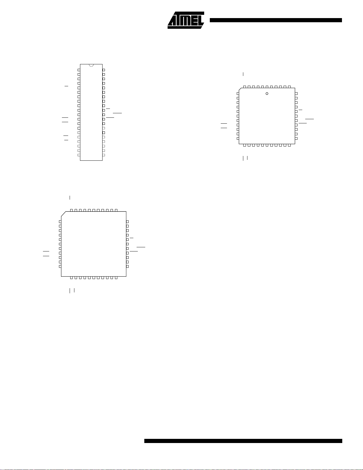
Pin Configurations
PDIP
1
(T2) P1.0
2
3
P1.2
4
P1.3
5
6
7
8
9
RST
10
11
12
13
14
(T0) P3.4
15
(T1) P3.5
16
17
18
XTAL2
19
XTAL1
20
GND
TQFP
P1.4 (SS)
P1.3
P1.2
P1.1 (T2 EX)
P1.0 (T2)NCVCC
4443424140393837363534
1213141516171819202122
(MOSI) P1.5
(MISO) P1.6
(SCK) P1.7
RST
(RXD) P3.0
(TXD) P3.1
(INT0) P3.2
(INT1) P3.3
(T0) P3.4
(T1) P3.5
(T2 EX) P1.1
(MOSI) P1.5
(MISO) P1.6
(SCK) P1.7
(RXD) P3.0
(TXD) P3.1
(INT0) P3.2
(INT1) P3.3
NC
(SS) P1.4
(WR) P3.6
(RD) P3.7
1
2
3
4
5
6
7
8
9
10
11
40
39
38
37
36
35
34
33
32
31
30
29
28
27
26
25
24
23
22
21
VCC
P0.0 (AD0)
P0.1 (AD1)
P0.2 (AD2)
P0.3 (AD3)
P0.4 (AD4)
P0.5 (AD5)
P0.6 (AD6)
P0.7 (AD7)
EA/VPP
ALE/PROG
PSEN
P2.7 (A15)
P2.6 (A14)
P2.5 (A13)
P2.4 (A12)
P2.3 (A11)
P2.2 (A10)
P2.1 (A9)
P2.0 (A8)
P0.0 (AD0)
P0.1 (AD1)
P0.2 (AD2)
P0.3 (AD3)
33
32
31
30
29
28
27
26
25
24
23
P0.4 (AD4)
P0.5 (AD5)
P0.6 (AD6)
P0.7 (AD7)
EA/VPP
NC
ALE/PROG
PSEN
P2.7 (A15)
P2.6 (A14)
P2.5 (A13)
(MOSI) P1.5
(MISO) P1.6
(SCK) P1.7
RST
(RXD) P3.0
(TXD) P3.1
(INT0) P3.2
(INT1) P3.3
(T0) P3.4
(T1) P3.5
PLCC
P1.4 (SS)
P1.3
P1.2
P1.1 (T2 EX)
65432
7
8
9
10
11
12
NC
13
14
15
16
17
1819202122232425262728
XTAL2
XTAL1
(RD) P3.7
(WR) P3.6
P1.0 (T2)NCVCC
1
4443424140
NC
GND
(A8) P2.0
P0.0 (AD0)
P0.1 (AD1)
P0.2 (AD2)
(A9) P2.1
(A10) P2.2
(A11) P2.3
P0.3 (AD3)
39
P0.4 (AD4)
38
P0.5 (AD5)
37
P0.6 (AD6)
36
P0.7 (AD7)
35
EA/VPP
34
NC
33
ALE/PROG
32
PSEN
31
P2.7 (A15)
30
P2.6 (A14)
29
P2.5 (A13)
(A12) P2.4
GND
GND
XTAL2
XTAL1
(A8) P2.0
(RD) P3.7
(WR) P3.6
(A9) P2.1
(A10) P2.2
(A11) P2.3
(A12) P2.4
Pin Description
V
CC
Supply voltage.
GND
Ground.
Port 0
Port 0 is an 8-bit open drain bidirectional I/O port. As an
output port, each pin can sink eight TTL inputs. When 1s
are written to port 0 pins, the pins can be used as highimpedance inputs.
Port 0 can also be configu red to be the multiplex ed loworder address/data bus during accesses to ex ternal program and data memory. In this mode, P0 has internal pullups.
4-138
AT89LS8252
Port 0 also receives the code bytes during Flash programming and outputs the code bytes durin g program verifica tion. External pullu ps are require d duri ng prog ram ve rifica tion.
Port 1
Port 1 is an 8-bit bidirectional I/O port with interna l pullups.
The Port 1 output buffers can sink/source four TTL inputs.
When 1s are writte n to Po rt 1 pi ns, they a re pul led high by
the internal pullups and can be used as inputs. As inputs,
Port 1 pins that are externally being pulled low will source
current (I
) because of the internal pullups.
IL
Some Port 1 pins p rovide additi onal functions. P1.0 and
P1.1 can be config ured to be th e timer/count er 2 ext ernal
count input (P1.0/T2) and the timer/counter 2 trigger input
(P1.1/T2EX), respectively.
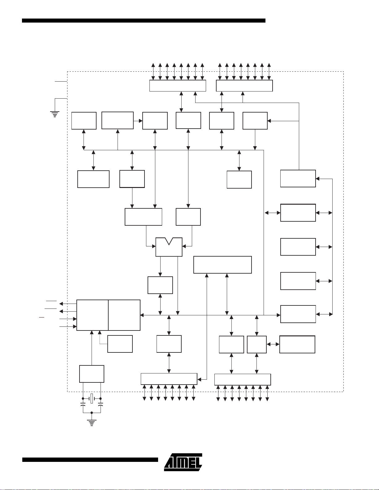
Block Diagram
AT89LS8252
V
CC
GND
EEPROM
REGISTER
B
RAM ADDR.
REGISTER
P0.0 - P0.7
PORT 0 DRIVERS
RAM
ACC
TMP2 TMP1
PORT 0
LATCH
P2.0 - P2.7
PORT 2 DRIVERS
PORT 2
LATCH
STACK
POINTER
FLASH
PROGRAM
ADDRESS
REGISTER
BUFFER
PSEN
ALE/PROG
EA / V
RST
PC
ALU
INTERRUPT, SERIAL PORT,
AND TIMER BLOCKS
PSW
TIMING
AND
PP
CONTROL
OSC
INSTRUCTION
REGISTER
WATCH
DOG
PORT 3
LATCH
PORT 3 DRIVERS
P3.0 - P3.7
PORT 1
LATCH
PORT 1 DRIVERS
P1.0 - P1.7
SPI
PORT
INCREMENTER
PROGRAM
COUNTER
DPTR
PROGRAM
LOGIC
4-139

Pin Description
Furthermore, P1.4, P1.5, P1.6, and P1.7 can be configured
as the SPI slave port select, data input/output and shift
clock input/output pins as shown in the following table.
Port Pin Alternate Functions
P1.0
P1.1
P1.4 SS
P1.5
T2 (external count input to Timer/Counter
2), clock-out
T2EX (Timer/Counter 2 capture/reload
trigger and direction control)
(Slave port select input)
MOSI (Master data output, slave data input
pin for SPI channel)
Port Pin Alternate Functions
P3.0 RXD (serial input port)
P3.1 TXD (serial output port)
P3.2 INT0
P3.3 INT1
P3.4 T0 (timer 0 external input)
P3.5 T1 (timer 1 external input)
P3.6 WR
P3.7 RD
(external interrupt 0)
(external interrupt 1)
(external data memory write s trobe)
(external data memory read strobe)
P1.6
P1.7
Port 1 also receives the low-order address bytes during
Flash programming and verification.
Port 2
Port 2 is an 8-bit bidire ction al I/O por t w ith inter nal pullu ps.
The Port 2 output buffers can sink/source four TTL inputs.
When 1s are written to Port 2 pins , they are p ulled hi gh by
the internal pullups and can be used as inputs. As inputs ,
Port 2 pins that are externally being pulled low will source
current (I
Port 2 emits the high-order address byte during fetches
from external program memory and during accesses to
external data memory that use 16-bit addre sses (MO VX @
DPTR). In this application, Port 2 uses strong internal pullups when emitting 1s. During accesses to external data
memory that use 8-bit addresses (MOVX @ RI), Port 2
emits the contents of the P2 Special Function Register.
Port 2 also receives the high-order address bits and some
control signals during Flash programming and verification.
Port 3
Port 3 is an 8 bit b idirec tional I/O port with i nternal pul lups.
The Port 3 output buffers can sink/source four TTL inputs.
When 1s are written to Port 3 pins , they are p ulled hi gh by
the internal pullups and can be used as inputs. As inputs ,
Port 3 pins that are externally being pulled low will source
current (I
Port 3 also se rves the fu nctio ns of vari ous sp ecial f eat ures
of the AT89LS8252, as shown in the following table.
Port 3 also receives some control signals for Flash programming and verification.
MISO (Master data input, slave data output
pin for SPI channel)
SCK (Master clock output, slave clock input
pin for SPI channel)
) because of the internal pullups.
IL
) because of the pullups.
IL
RST
Reset input. A high on this pin for two machine cycles while
the oscillator is running resets the device.
ALE/PROG
Address Latch Enable is an output pulse for latching the
low byte of the address during accesses to external memory. This pin is also the program pulse input (PROG
Flash programming.
In normal operation, ALE is emitte d at a con stant rate of 1/
6 the oscillator frequency and may be used for external timing or clocking purposes. Note, however, that one ALE
pulse is skipped d ur in g ea ch ac c ess to ex ter na l d ata mem ory.
If desired, ALE operation can be disabled by setting bit 0 of
SFR location 8 EH. With the bit se t, ALE is activ e only du ring a MOVX or MOVC instruction. Otherwise, the pin is
weakly pulled high. Setting the ALE-disable bit has no
effect if the microcontroller is in external execution mode.
PSEN
Program Store Enable is the read strobe to external program memory.
When the AT89LS8252 is executing code from external
program memory, PSEN
cycle, except that two PSEN
each access to external data memory.
/V
EA
PP
External Access Enable. EA must be strapped to GND in
order to enable the device to fetch code from external program memory locations starting at 0000H up to FFFFH.
Note, however, that if lock bit 1 is programmed, EA
internally latched on reset.
should be strapped to VCC for internal program execu-
EA
tions. This pin also recei ves the 12-volt programmi ng
enable voltage ( V
volt programming is selected.
PP
is activated twice each machine
activations are skipped during
) during Flash prog ramming when 12-
) during
will be
4-140
AT89LS8252

AT89LS8252
XTAL1
Input to the inverting os cillator ampl ifier and input to the
internal clock operating circuit.
XTAL2
Output from the inverting oscillator amplifier.
Special Function Registers
A map of the on-chip memory area called the Special Function Register (SFR) space is shown in Table 1.
Note that not all of the address es are occupied, and unoccupied addresses may not be implemented on the chip.
Read accesses to these addresses will in general return
random data, and write accesses will have an indeterminate
effect.
Table 1.
0F8H 0FFH
0F0H
0E8H 0EFH
0E0H
0D8H 0DFH
0D0H
0C8H
AT89LS8252 SFR Map and Reset Values
B
00000000
ACC
00000000
PSW
00000000
T2CON
00000000
T2MOD
XXXXXX00
RCAP2L
00000000
RCAP2H
00000000
TL2
00000000
SPCR
000001XX
TH2
00000000
0F7H
0E7H
0D7H
0CFH
0C0H 0C7H
0B8H
0B0H
0A8H
0A0H
98H
90H
88H
80H
IP
XX000000
P3
11111111
IE
0X000000
P2
11111111
SCON
00000000
P1
11111111
TCON
00000000
P0
11111111
SBUF
XXXXXXXX
TMOD
00000000
SP
00000111
SPSR
00XXXXXX
TL0
00000000
DP0L
00000000
TL1
00000000
DP0H
00000000
TH0
00000000
DP1L
00000000
TH1
00000000
DP1H
00000000
WMCON
00000010
SPDR
XXXXXXXX
PCON
0XXX0000
0BFH
0B7H
0AFH
0A7H
9FH
97H
8FH
87H
4-141

User software shou ld not write 1s to these unlisted locations, since they may be u sed in future products to invoke
new features. In that case, the reset or inactive values of the
new bits will always be 0.
Timer 2 Registers
registers T2CON (shown in Table 2) and T2MOD (shown in
Table 9) for Timer 2. The register pa ir (RC AP 2H, RCA P2 L)
are the Capture/Reload registers for Timer 2 in 16 bit capture mode or 16-bit auto-reload mode.
Watchdog and Memory Control Register
register contains control bits for the Watchdog Timer
(shown in Table 3). The EEMEN and EEMWE bits are used
to select the 2K bytes on-chip EEPROM, and to enable
byte-write. Th e DPS b it selec ts one o f two DP TR registe rs
available.
Control and status b its ar e con tai ned in
The WMCON
SPI Registers
eral Interface are contained in registers SPCR (shown in
Table 4) and SPSR (shown in Table 5). The SPI data bits
are contained in the SPDR register. Writing the SPI data
register during serial data transfer sets the Write Collision
bit, WCOL, in the SPSR register. The SPDR is double buffered for writing and the values in SPDR are not changed by
Reset.
Interrupt Registers
individual interrupt enable bits are in the IE register. In addition, the individual interrupt enable bit for the SPI is in the
SPCR register. Two priorities ca n be set for each of the si x
interrupt sources in the IP register.
Control and status bits for the Serial Periph-
The global interrupt enable bit and the
Table 2.
T2CON Address = 0C8H Reset Value = 0000 0000B
Bit Addressable
Symbol Function
TF2
EXF2
RCLK
TCLK
EXEN2
T2CON—Timer/Counter 2 Control Register
TF2 EXF2 RCLK TCLK EXEN2 TR2 C/T2
Bit76543210
Timer 2 overflow flag set by a Timer 2 overflow and must be cleared by software. TF2 will not be set when
either RCLK = 1 or TCLK = 1.
Timer 2 external flag set when either a capture or reload is caused by a negative transition on T2EX and
EXEN2 = 1. When Timer 2 interrupt is enabled, EXF2 = 1 will cause the CPU to vector to the Timer 2 interrupt
routine. EXF2 must be cleared by software. EXF2 does not cause an interrupt in up/down counter mode
(DCEN = 1).
Receive clock enable. When set, causes the serial port to use Timer 2 overflow pulses for its receive clock in
serial port Modes 1 and 3. RCLK = 0 causes Timer 1 overflows to be used for the receive clock.
Transmit clock enable. When set, causes the serial port to use Timer 2 overflow pulses for its transmit clock in
serial port Modes 1 and 3. TCLK = 0 causes Timer 1 overflows to be used for the transmit clock.
Timer 2 external enable. When set, allows a capture or reload to occur as a result of a negative transition on
T2EX if Timer 2 is not being used to clock the serial port. EXEN2 = 0 causes Timer 2 to ignore events at
T2EX.
CP/RL2
TR2 Start/Stop control for Timer 2. TR2 = 1 starts the timer.
C/T2
CP/RL2
4-142
Timer or counter select for Timer 2. C/T2 = 0 for timer function. C/T2 = 1 for external event counter (falling
edge triggered).
Capture/Reload select. CP/RL2 = 1 causes captures to occur on negative transitions at T2EX if EXEN2 = 1.
CP/RL2
when EXEN2 = 1. When either RCLK or TCLK = 1, this bit is ignored and the timer is forced to auto-reload on
Timer 2 overflow.
= 0 causes automatic reloads to occur when Timer 2 overflows or negative transitions occur at T2EX
AT89LS8252

AT89LS8252
Dual Data Pointer Registers
internal EEPROM and ex ternal dat a memor y, two ba nks o f
16 bit Data P ointer Re gisters are prov ided: DP0 at SF R
address locations 82H-83H and DP1 at 84H-85H. Bit DPS
= 0 in SFR WMCON selects DP0 and DPS = 1 selects
DP1. The user should always initialize the DPS bit to the
Table 3.
WMCON Address = 96H Reset Value = 0000 0010B
Bit76543210
Symbol Function
PS2
PS1
PS0
EEMWE EEPROM Data Memory Write Enable Bit. Set this bit to “1” before initiating byte write to on-chip EEPROM
EEMEN Internal EEPROM Access Enable. When EEMEN = 1, the MOVX instruction with DPTR will access on-chip
WMCON—Watchdog and Memory Control Register
PS2 PS1 PS0 EEMWE EEMEN DPS WDTRST WDTEN
Prescaler Bits for the Watchdog Timer. When all three bits are set to “0”, the watchdog timer has a nominal
period of 16 ms. When all three bits are set to “1”, the nominal period is 2048 ms.
with the MOVX instruction. User software should set this bit to “0” after EEPROM write is completed.
EEPROM instead of external data memory. When EEMEN = 0, MOVX with DPTR accesses external data
memory.
To facilitate accessing both
appropriate value before accessing the respective Data
Pointer Register.
Power Off Flag
bit_4 (PCON.4) in the PC ON SF R. POF is set to “1” duri ng
power up. It can be set and reset under software control
and is not affected by RESET.
The Power Off Flag (POF) is located at
DPS Data Pointer Register Select. DPS = 0 selects the first bank of Data Pointer Register, DP0, and DPS = 1
selects the second bank, DP1
WDTRST
RDY/BSY
WDTEN Watchdog Timer Enable Bit. WDTEN = 1 enables the watchdog timer and WDTEN = 0 disables the
Watchdog Timer Reset and EEPROM Ready/Busy Flag. Each time this bit is set to “1” by user software, a
pulse is generated to reset the watchdog timer. The WDTRST bit is then automatically reset to “0” in the
next instruction cycle. The WDTRST bit is Write-Only. This bit also serves as the RDY/BSY
Only mode during EEPROM write. RDY/BSY
While programming operations are being executed, the RD Y/BSY
“1” when programming is completed.
watchdog timer.
= 1 means that the EEPROM is ready to be programmed.
bit equals “0” and is automatically reset to
flag in a Read-
4-143

Table 4
. SPCR—SPI Control Register
SPCR Address = D5H Reset V alue = 0000 01XXB
SPIE SPE DORD MSTR CPOL CPHA SPR1 SPR0
Bit76543210
Symbol Function
SPIE SPI Interrupt Enable. This bit, in conjunction with the ES bit in the IE register, enables SPI interrupts: SPIE
= 1 and ES = 1 enable SPI interrupts. SPIE = 0 disables SPI interrupts.
SPE SPI Enable. SPI = 1 enables the SPI channel and connects SS
P1.6, and P1.7. SPI = 0 disables the SPI channel.
DORD Data Order. DORD = 1 selects LSB first data transmission. DORD = 0 selects MSB first data transmission.
MSTR Master/Slave Select. MSTR = 1 selects Master SPI mode. MSTR = 0 selects Slave SPI mode.
CPOL Clock Polarity. When CPOL = 1, SCK is high when idle. When CPOL = 0, SCK of the master device is low
when not transmitting. Please refer to figure on SPI Clock Phase and Polarity Control.
CPHA Clock Phase. The CPHA bit together with the CPOL bit controls the clock and data relationship between
master and slave. Please refer to figure on SPI Clock Phase and Polarity Control.
SPR0
SPR1
Table 5.
SPSR Address = AAH Reset Value = 00XX XXXXB
SPI Clock Rate Select. These two bits control the SCK rate of the device configured as master. SPR1 and
SPR0 have no effect on the slave. The relationship between SCK and the oscillator frequency, F
follows:
SPR1 SPR0 SCK = F
00 4
01 16
10 64
11 128
SPSR—SPI Status Register
divided by
OSC.
, MOSI, MISO and SCK to pins P1.4, P1.5,
, is as
OSC.
SPIFWCOL——————
Bit76543210
Symbol Function
SPIF SPI Interrupt Flag. When a serial transfer is complete, the SPIF bit is set and an interrupt is generated if
SPIE = 1 and ES = 1. The SPIF bit is cleared by reading the SPI status register with SPIF and WCOL bits
set, and then accessing the SPI data register.
WCOL Write Collision Flag. The WCOL bit is set if the SPI data register is written during a data transfer. During
data transfer, the result of reading the SPDR register may be incorrect, and writing to it has no effect. The
WCOL bit (and the SPIF bit) are cleared by reading the SPI status register with SPIF and WCOL set, and
then accessing the SPI data register.
4-144
AT89LS8252

AT89LS8252
Table 6.
SPDR Address = 86H Reset V alue = unchanged
SPDR—SPI Data Register
SPD7 SPD6 SPD5 SPD4 SPD3 SPD2 SPD1 SPD0
Bit76543210
Data Memory—EEPROM and RAM
The AT89LS8252 implements 2K bytes of on-chip
EEPROM for data st orage and 256 bytes of RAM. The
upper 128 bytes of RAM occupy a parallel space to the
Special Function Register s. That means the u pper 128
bytes have the same addresses as the SFR space but are
physically separate from SFR space.
When an instruction accesses an internal location above
address 7FH, the address mode used in the instruction
specifies whether the CPU accesses the upper 128 bytes
of RAM or the SFR space. Instructions that use direct
addressing access SFR space.
For example, the following direct addressing instruction
accesses the SFR at location 0A0H (which is P2).
MOV 0A0H, #data
Instructions that use indirect addressing access the upper
128 bytes of RAM. For example, the following indirect
addressing instru ct ion , where R0 contains 0A0H, acc es s es
the data byte at address 0A0H, rather than P2 (whose
address is 0A0H).
MOV @R0, #data
Note that stack operations are examples of indirect
addressing, so the upper 128 byte s of data RAM are avail able as stack space.
The on-chip EEPROM data memory is selected by setting
the EEMEN bit in the WMCON register at SFR address
location 96H. The EEPROM address range is from 000H to
7FFH. The MOVX instructions ar e used to access the
EEPROM. To access off-chip data memory with the MOVX
instructions, the EEMEN bit needs to be set to “0”.
The EEMWE bit in the WMCON register need s to be set to
“1” before any byte location in the EEPROM can be written.
User software should res et EEMWE bit to “0” if no further
EEPROM write is requi red. EEPROM write cycl es in the
serial programming mode are self-timed and typically take
2.5 ms. The progress of EEPROM write can be monitored
by reading the RDY/BSY
RDY/BSY
RDY/BSY
and another write cycle can be initiated.
= 0 means programming is still in progress and
= 1 means EEPROM write cycle is completed
bit (read-only) in SFR WM CON.
In addition, during EEPROM programming, an attempted
read from the EEPROM will fetch the byte being written
with the MSB c omple mente d. O nce t he wr ite c ycle is c ompleted, true data are valid at all bit locations.
Programmable Watchdog Timer
The programmable Watchdog Timer (WDT) operates from
an independent oscillator. T he prescaler bits, PS0, PS1
and PS2 in SFR WMCON ar e use d to se t the peri od of the
Watchdog Timer from 16 ms to 2048 ms. The available
timer periods are shown in the following table and the
actual timer periods (at V
nominal.
The WDT is disabled by Power-on Reset and during Power
Down. It is enable d by setting the WDTE N bit in SFR
WMCON (address = 96H). The W D T is re se t by sett in g the
WDTRST bit in WMCON. When the WDT times out without
being reset or disabled, an in terna l RST pu ls e is gene rated
to reset the CPU.
Table 7.
Watchdog Timer Period Selection
WDT Prescaler Bits
PS2 PS1 PS0
0 0 0 16 ms
0 0 1 32 ms
0 1 0 64 ms
0 1 1 128 ms
1 0 0 256 ms
1 0 1 512 ms
1 1 0 1024 ms
1 1 1 2048 ms
= 5V) are within ±30% of the
CC
Period (nominal)
4-145
Timer 0 and 1
Timer 0 and Timer 1 in the AT89LS 8252 ope rate the s ame
way as Timer 0 and Timer 1 in the AT89C51, AT89C52 and
AT89C55. For further information, see the October 1995
Microcontroller Data Book, page 2-4 5, section titled,
“Timer/Counters.”
Table 8.
Timer 2 Operating Modes
RCLK + TCLK CP/RL2
0 0 1 16-bit Auto-Reload
0 1 1 16-bit Capture
TR2 MODE
Timer 2
Timer 2 is a 16 bit Timer/Counter that can operate as either
a timer or an event counter. The type of operation is
selected by bit C/T2
Timer 2 has three operating modes: capture, auto-reload
(up or down counting), and baud rate generator. The
modes are selected by bits in T2CON, as shown in Table 8.
Timer 2 consists of two 8- bi t regi st er s, TH2 and TL2. I n the
Timer function, the TL2 r egister is incremented ever y
machine cycle. Since a machine cycle consists of 12 oscillator periods, the count rate is 1/12 of the oscillator frequency.
In the Counter function, the register is incremented in
response to a 1-to-0 transition at its corresponding external
input pin, T2. In thi s func tion, the extern al i nput is sa mpled
during S5P2 of every machin e cycle. When the samples
show a high in one cycle and a low in the next cycle, the
count is incremented. The new count value appears in the
register during S3P1 of the cycle following the one in which
the transition was detected. Since two machine cycles (24
oscillator periods ) ar e requi r ed to r ec og niz e a 1 -t o- 0 tran si tion, the maximum count rate is 1/24 of the oscillator frequency. To ensure that a gi ven level is sam pled at least
once before it changes, the level should be held for at least
one full machine cycle.
in the SFR T2 C ON (sh o w n i n Ta bl e 2).
1X1
Baud Rate
Generator
X X 0 (Off)
Capture Mode
In the capture mode, two options are selected by bit
EXEN2 in T2CON. If EXEN2 = 0, Timer 2 is a 16 bit timer
or counter which upon overflow sets bit TF2 in T2CON.
This bit can then be used to generate an interrupt. If
EXEN2 = 1, Timer 2 p er forms t he sa me operation, but a 1 to-0 transition at external input T2EX also causes the current value in TH2 and TL2 to be captured into RCAP2H and
RCAP2L, resp ective ly. In addi tion, th e transit ion at T2E X
causes bit EXF2 in T2CON to be set. The EXF2 bit, like
TF2, can generate an interrupt. The capture mode is illustrated in Figure 1.
Auto-Reload (Up or Down Counter)
Timer 2 can be programmed to count up or down when
configured in its 16 bit auto-reload mode. This feature is
invoked by the DCEN (Down Counter Enable) bit located in
the SFR T2MOD (see Table 9). Upon reset, the DCEN bit
is set to 0 so that ti mer 2 will defa ult to count u p. When
DCEN is set, Timer 2 can coun t up or down, depend ing on
the value of the T2EX pin.
Figure 1.
OSC
T2EX PIN
4-146
Timer 2 in Capture Mode
÷12
T2 PIN
TRANSITION
DETECTOR
AT89LS8252
C/T2 = 0
C/T2 = 1
EXEN2
CONTROL
TR2
CAPTURE
CONTROL
TH2 TL2
RCAP2LRCAP2H
EXF2
TF2
OVERFLOW
TIMER 2
INTERRUPT
 Loading...