


BDTIC www.bdtic.com/ATMEL
Features
• Compatible with MCS
• 4K Bytes of In-System Programmable (ISP) Flash Memory
– Endurance: 1000 Write/Erase Cycles
• 2.7V to 4.0V Operating Range
• Fully Static Operation: 0 Hz to 16 MHz
• Three-level Program Memory Lock
• 128 x 8-bit Internal RAM
• 32 Programmable I/O Lines
• Two 16-bit Timer/Counters
• Six Interrupt Sources
• Full Duplex UART Serial Channel
• Low-power Idle and Power-down Modes
• Interrupt Recovery from Power-down Mode
• Watchdog Timer
• Dual Data Pointer
• Power-off Flag
• Flexible ISP Programming (Byte and Page Mode)
• Green (Pb/Halide-free) Packaging Option
®
-51 Products
8-bit
Low-Voltage
Microcontroller
with 4K Bytes
In-System
Programmable
1. Description
The AT89LS51 is a low-voltage, high-performance CMOS 8-bit microcontroller with
4K bytes of in-system programmable Flash memory. The device is manufactured
using Atmel’s high-density nonvolatile memory technology and is compatible with the
industry-standard 80C51 instruction set and pinout. The on-chip Flash allows the program memory to be reprogrammed in-system or by a conventional nonvolatile
memory programmer. By combining a versatile 8-bit CPU with in-system programmable Flash on a monolithic chip, the Atmel AT89LS51 is a powerful microcontroller
which provides a highly-flexible and cost-effective solution to many embedded control
applications.
The AT89LS51 provides the following standard features: 4K bytes of Flash, 128 bytes
of RAM, 32 I/O lines, Watchdog timer, two data pointers, two 16-bit timer/counters, a
five-vector two-level interrupt architecture, a full duplex serial port, on-chip oscillator,
and clock circuitry. In addition, the AT89LS51 is designed with static logic for operation down to zero frequency and supports two software selectable power saving
modes. The Idle Mode stops the CPU while allowing the RAM, timer/counters, serial
port, and interrupt system to continue functioning. The Power-down mode saves the
RAM contents but freezes the oscillator, disabling all other chip functions until the next
external interrupt or hardware reset.
Flash
AT89LS51
3053B–MICRO–3/05
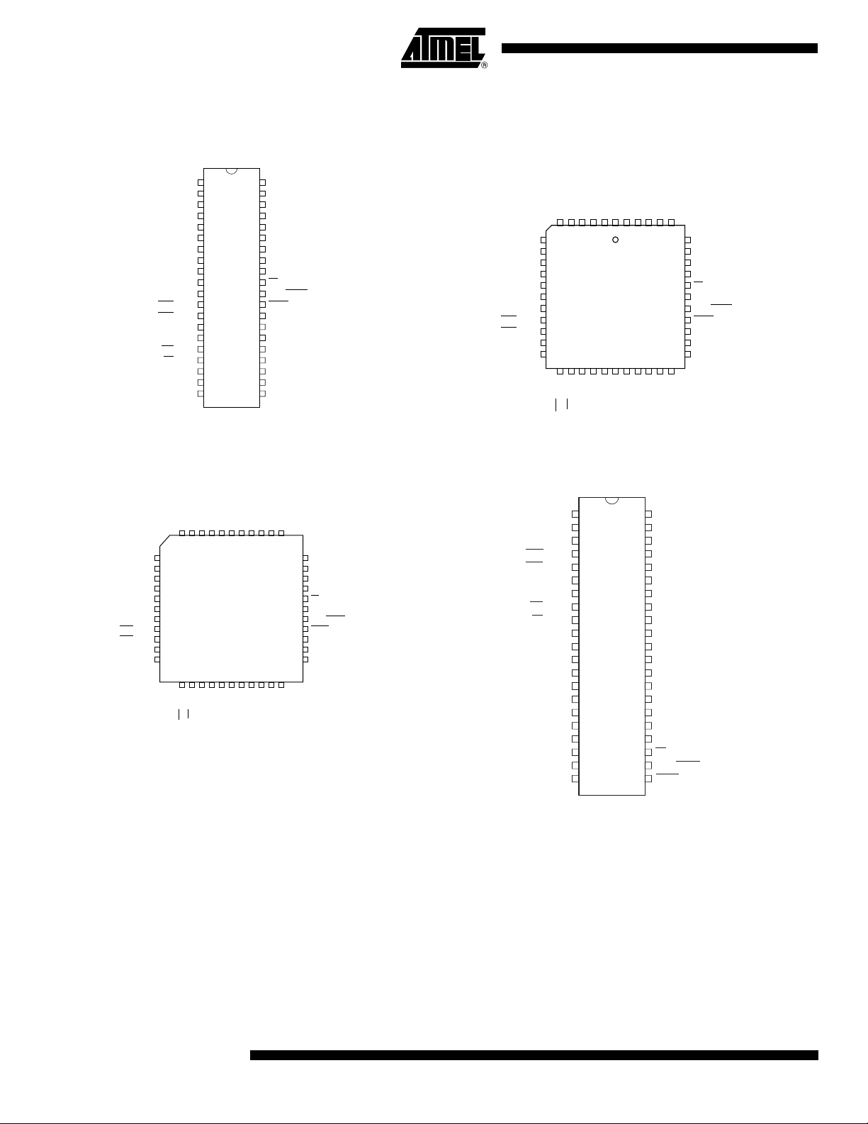
2. Pin Configurations
2.1 40-lead PDIP
P1.0
P1.1
P1.2
P1.3
P1.4
(MOSI) P1.5
(MISO) P1.6
(SCK) P1.7
RST
(RXD) P3.0
(TXD) P3.1
(INT0) P3.2
(INT1) P3.3
(T0) P3.4
(T1) P3.5
(WR) P3.6
(RD) P3.7
XTAL2
XTAL1
GND
2.2 44-lead TQFP
P1.4
P1.3
4443424140393837363534
RST
(T0) P3.4
(T1) P3.5
1
2
3
4
5
6
NC
7
8
9
10
11
1213141516171819202122
(RD) P3.7
(WR) P3.6
(MOSI) P1.5
(MISO) P1.6
(SCK) P1.7
(RXD) P3.0
(TXD) P3.1
(INT0) P3.2
(INT1) P3.3
1
2
3
4
5
6
7
8
9
10
11
12
13
14
15
16
17
18
19
20
P1.2
XTAL2
P1.1
P1.0 NCVCC
GND
XTAL1
GND
40
39
38
37
36
35
34
33
32
31
30
29
28
27
26
25
24
23
22
21
P0.0 (AD0)
(A8) P2.0
(A9) P2.1
VCC
P0.0 (AD0)
P0.1 (AD1)
P0.2 (AD2)
P0.3 (AD3)
P0.4 (AD4)
P0.5 (AD5)
P0.6 (AD6)
P0.7 (AD7)
EA/VPP
ALE/PROG
PSEN
P2.7 (A15)
P2.6 (A14)
P2.5 (A13)
P2.4 (A12)
P2.3 (A11)
P2.2 (A10)
P2.1 (A9)
P2.0 (A8)
P0.1 (AD1)
P0.2 (AD2)
P0.3 (AD3)
(A10) P2.2
(A11) P2.3
(A12) P2.4
33
32
31
30
29
28
27
26
25
24
23
P0.4 (AD4)
P0.5 (AD5)
P0.6 (AD6)
P0.7 (AD7)
EA/VPP
NC
ALE/PROG
PSEN
P2.7 (A15)
P2.6 (A14)
P2.5 (A13)
2.3 44-lead PLCC
P1.4
65432
(MOSI) P1.5
(MISO) P1.6
(SCK) P1.7
(RXD) P3.0
(TXD) P3.1
(INT0) P3.2
(INT1) P3.3
(T0) P3.4
(T1) P3.5
7
8
9
10
RST
11
12
NC
13
14
15
16
17
1819202122232425262728
(WR) P3.6
2.4 42-lead PDIP
RST
(RXD) P3.0
(TXD) P3.1
(INT0) P3.2
(INT1) P3.3
(T0) P3.4
(T1) P3.5
(WR) P3.6
(RD) P3.7
XTAL2
XTAL1
GND
PWRGND
(A8) P2.0
(A9) P2.1
(A10) P2.2
(A11) P2.3
(A12) P2.4
(A13) P2.5
(A14) P2.6
(A15) P2.7
P1.3
P1.2
P1.1
XTAL2
XTAL1
(RD) P3.7
1
2
3
4
5
6
7
8
9
10
11
12
13
14
15
16
17
18
19
20
21
P1.0 NCVCC
1
4443424140
NC
GND
(A8) P2.0
42
41
40
39
38
37
36
35
34
33
32
31
30
29
28
27
26
25
24
23
22
P0.0 (AD0)
P0.1 (AD1)
P0.2 (AD2)
(A9) P2.1
(A10) P2.2
(A11) P2.3
P1.7 (SCK)
P1.6 (MISO)
P1.5 (MOSI)
P1.4
P1.3
P1.2
P1.1
P1.0
VDD
PWRVDD
P0.0 (AD0)
P0.1 (AD1)
P0.2 (AD2)
P0.3 (AD3)
P0.4 (AD4)
P0.5 (AD5)
P0.6 (AD6)
P0.7 (AD7)
EA/VPP
ALE/PROG
PSEN
P0.3 (AD3)
39
P0.4 (AD4)
38
P0.5 (AD5)
37
P0.6 (AD6)
36
P0.7 (AD7)
35
EA/VPP
34
NC
33
ALE/PROG
32
PSEN
31
P2.7 (A15)
30
P2.6 (A14)
29
P2.5 (A13)
(A12) P2.4
2
AT89LS51
3053B–MICRO–3/05
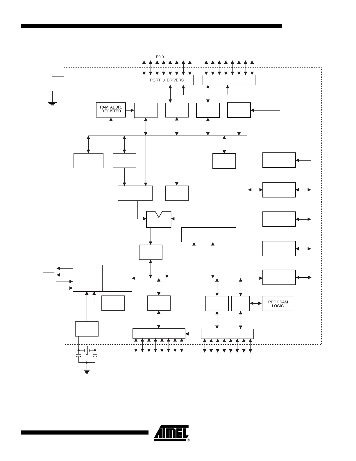
3. Block Diagram
AT89LS51
V
CC
GND
B
REGISTER
RAM ADDR.
REGISTER
P0.0 - P0.7
PORT 0 DRIVERS
RAM
ACC
TMP2 TMP1
ALU
PORT 0
LATCH
PORT 2 DRIVERS
PORT 2
LATCH
POINTER
P2.0 - P2.7
FLASH
STACK
PROGRAM
ADDRESS
REGISTER
BUFFER
PC
INCREMENTER
PSEN
ALE/PROG
EA / V
RST
INTERRUPT, SERIAL PORT,
AND TIMER BLOCKS
PROGRAM
PSW
TIMING
AND
PP
CONTROL
OSC
INSTRUCTION
REGISTER
WATCH
DOG
PORT 3
LATCH
PORT 3 DRIVERS
P3.0 - P3.7
PORT 1
LATCH
PORT 1 DRIVERS
P1.0 - P1.7
ISP
PORT
COUNTER
DUAL DPTR
PROGRAM
LOGIC
3053B–MICRO–3/05
3

4. Pin Description
4.1 VCC
Supply voltage.
4.2 GND
Ground.
4.3 Port 0
Port 0 is an 8-bit open drain bidirectional I/O port. As an output port, each pin can sink eight TTL
inputs. When 1s are written to port 0 pins, the pins can be used as high-impedance inputs.
Port 0 can also be configured to be the multiplexed low-order address/data bus during accesses
to external program and data memory. In this mode, P0 has internal pull-ups.
Port 0 also receives the code bytes during Flash programming and outputs the code bytes during program verification. External pull-ups are required during program verification.
4.4 Port 1
Port 1 is an 8-bit bidirectional I/O port with internal pull-ups. The Port 1 output buffers can
sink/source four TTL inputs. When 1s are written to Port 1 pins, they are pulled high by the internal pull-ups and can be used as inputs. As inputs, Port 1 pins that are externally being pulled low
will source current (I
Port 1 also receives the low-order address bytes during Flash programming and verification.
) because of the internal pull-ups.
IL
4.5 Port 2
Port Pin Alternate Functions
P1.5 MOSI (used for In-System Programming)
P1.6 MISO (used for In-System Programming)
P1.7 SCK (used for In-System Programming)
Port 2 is an 8-bit bidirectional I/O port with internal pull-ups. The Port 2 output buffers can
sink/source four TTL inputs. When 1s are written to Port 2 pins, they are pulled high by the internal pull-ups and can be used as inputs. As inputs, Port 2 pins that are externally being pulled low
will source current (I
Port 2 emits the high-order address byte during fetches from external program memory and during accesses to external data memory that use 16-bit addresses (MOVX @ DPTR). In this
application, Port 2 uses strong internal pull-ups when emitting 1s. During accesses to external
data memory that use 8-bit addresses (MOVX @ RI), Port 2 emits the contents of the P2 Special
Function Register.
Port 2 also receives the high-order address bits and some control signals during Flash programming and verification.
) because of the internal pull-ups.
IL
4
AT89LS51
3053B–MICRO–3/05
4.6 Port 3
AT89LS51
Port 3 is an 8-bit bidirectional I/O port with internal pull-ups. The Port 3 output buffers can
sink/source four TTL inputs. When 1s are written to Port 3 pins, they are pulled high by the internal pull-ups and can be used as inputs. As inputs, Port 3 pins that are externally being pulled low
will source current (I
Port 3 receives some control signals for Flash programming and verification.
Port 3 also serves the functions of various special features of the AT89LS51, as shown in the
following table.
Port Pin Alternate Functions
P3.0 RXD (serial input port)
P3.1 TXD (serial output port)
) because of the pull-ups.
IL
4.7 RST
4.8 ALE/PROG
P3.2 INT0
P3.3 INT1 (external interrupt 1)
P3.4 T0 (timer 0 external input)
P3.5 T1 (timer 1 external input)
P3.6 WR
P3.7 RD
(external interrupt 0)
(external data memory write strobe)
(external data memory read strobe)
Reset input. A high on this pin for two machine cycles while the oscillator is running resets the
device. This pin drives High for 98 oscillator periods after the Watchdog times out. The DISRTO
bit in SFR AUXR (address 8EH) can be used to disable this feature. In the default state of bit
DISRTO, the RESET HIGH out feature is enabled.
Address Latch Enable (ALE) is an output pulse for latching the low byte of the address during
accesses to external memory. This pin is also the program pulse input (PROG
) during Flash
programming.
In normal operation, ALE is emitted at a constant rate of 1/6 the oscillator frequency and may be
used for external timing or clocking purposes. Note, however, that one ALE pulse is skipped during each access to external data memory.
4.9 PSEN
3053B–MICRO–3/05
If desired, ALE operation can be disabled by setting bit 0 of SFR location 8EH. With the bit set,
ALE is active only during a MOVX or MOVC instruction. Otherwise, the pin is weakly pulled high.
Setting the ALE-disable bit has no effect if the microcontroller is in external execution mode.
Program Store Enable (PSEN) is the read strobe to external program memory.
When the AT89LS51 is executing code from external program memory, PSEN
each machine cycle, except that two PSEN
activations are skipped during each access to exter-
is activated twice
nal data memory.
5

4.10 EA/VPP
External Access Enable. EA must be strapped to GND in order to enable the device to fetch
code from external program memory locations starting at 0000H up to FFFFH. Note, however,
that if lock bit 1 is programmed, EA
should be strapped to VCC for internal program executions.
EA
will be internally latched on reset.
This pin also receives the 12-volt programming enable voltage (V
4.11 XTAL1
Input to the inverting oscillator amplifier and input to the internal clock operating circuit.
4.12 XTAL2
Output from the inverting oscillator amplifier
5. Special Function Registers
A map of the on-chip memory area called the Special Function Register (SFR) space is shown in
Table 5-1.
Note that not all of the addresses are occupied, and unoccupied addresses may not be implemented on the chip. Read accesses to these addresses will in general return random data, and
write accesses will have an indeterminate effect.
) during Flash programming.
PP
6
AT89LS51
3053B–MICRO–3/05

AT89LS51
Table 5-1. AT89LS51 SFR Map and Reset Values
0F8H 0FFH
0F0H
0E8H 0EFH
0E0H
0D8H 0DFH
0D0H
0C8H 0CFH
0C0H 0C7H
0B8H
0B0H
0A8H
0A0H
98H
90H
88H
80H
B
00000000
ACC
00000000
PSW
00000000
IP
XX000000
P3
11111111
IE
0X000000
P2
11111111
SCON
00000000
P1
11111111
TCON
00000000
P0
11111111SP00000111
SBUF
XXXXXXXX
TMOD
00000000
AUXR1
XXXXXXX0
TL0
00000000
DP0L
00000000
TL1
00000000
DP0H
00000000
TH0
00000000
DP1L
00000000
TH1
00000000
DP1H
00000000
WDTRST
XXXXXXXX
AUXR
XXX00XX0
PCON
0XXX0000
0F7H
0E7H
0D7H
0BFH
0B7H
0AFH
0A7H
9FH
97H
8FH
87H
User software should not write 1s to these unlisted locations, since they may be used in future products to invoke new features. In that case, the reset or inactive values of the new bits will always be 0.
Interrupt Registers: The individual interrupt enable bits are in the IE register. Two priorities can be set for each of the five
interrupt sources in the IP register.
7
3053B–MICRO–3/05

Table 5-2. AUXR: Auxiliary Register
AUXR Address = 8EH Reset Value = XXX00XX0B
Not Bit
Addressable
– – – WDIDLE DISRTO – – DISALE
Bit
– Reserved for future expansion
DISALE Disable/Enable ALE
DISRTO Disable/Enable Reset out
WDIDLE Disable/Enable WDT in IDLE mode
765 4 3 2 1 0
DISALE
Operating Mode
0 ALE is emitted at a constant rate of 1/6 the oscillator frequency
1 ALE is active only during a MOVX or MOVC instruction
DISRTO
0 Reset pin is driven High after WDT times out
1 Reset pin is input only
WDIDLE
0 WDT continues to count in IDLE mode
1 WDT halts counting in IDLE mode
Dual Data Pointer Registers: To facilitate accessing both internal and external data memory,
two banks of 16-bit Data Pointer Registers are provided: DP0 at SFR address locations 82H83H and DP1 at 84H-85H. Bit DPS = 0 in SFR AUXR1 selects DP0 and DPS = 1 selects DP1.
The user should always initialize the DPS bit to the appropriate value before accessing the
respective Data Pointer Register.
Power Off Flag: The Power Off Flag (POF) is located at bit 4 (PCON.4) in the PCON SFR. POF
is set to “1” during power up. It can be set and rest under software control and is not affected by
reset.
8
AT89LS51
3053B–MICRO–3/05
Table 5-3. AUXR1: Auxiliary Register 1
AUXR1
Address = A2H
Not Bit
Addressable
––––– – – DPS
Bit 7 6 5 4 3 2 1 0
– Reserved for future expansion
DPS Data Pointer Register Select
DPS
0 Selects DPTR Registers DP0L, DP0H
1 Selects DPTR Registers DP1L, DP1H
6. Memory Organization
MCS-51 devices have a separate address space for Program and Data Memory. Up to 64K
bytes each of external Program and Data Memory can be addressed.
AT89LS51
Reset Value = XXXXXXX0B
6.1 Program Memory
If the EA pin is connected to GND, all program fetches are directed to external memory.
On the AT89LS51, if EA
FFFH are directed to internal memory and fetches to addresses 1000H through FFFFH are
directed to external memory.
is connected to VCC, program fetches to addresses 0000H through
6.2 Data Memory
The AT89LS51 implements 128 bytes of on-chip RAM. The 128 bytes are accessible via direct
and indirect addressing modes. Stack operations are examples of indirect addressing, so the
128 bytes of data RAM are available as stack space.
7. Watchdog Timer (One-time Enabled with Reset-out)
The WDT is intended as a recovery method in situations where the CPU may be subjected to
software upsets. The WDT consists of a 14-bit counter and the Watchdog Timer Reset
(WDTRST) SFR. The WDT is defaulted to disable from exiting reset. To enable the WDT, a user
must write 01EH and 0E1H in sequence to the WDTRST register (SFR location 0A6H). When
the WDT is enabled, it will increment every machine cycle while the oscillator is running. The
WDT timeout period is dependent on the external clock frequency. There is no way to disable
the WDT except through reset (either hardware reset or WDT overflow reset). When WDT overflows, it will drive an output RESET HIGH pulse at the RST pin.
3053B–MICRO–3/05
9

7.1 Using the WDT
To enable the WDT, a user must write 01EH and 0E1H in sequence to the WDTRST register
(SFR location 0A6H). When the WDT is enabled, the user needs to service it by writing 01EH
and 0E1H to WDTRST to avoid a WDT overflow. The 14-bit counter overflows when it reaches
16383 (3FFFH), and this will reset the device. When the WDT is enabled, it will increment every
machine cycle while the oscillator is running. This means the user must reset the WDT at least
every 16383 machine cycles. To reset the WDT the user must write 01EH and 0E1H to
WDTRST. WDTRST is a write-only register. The WDT counter cannot be read or written. When
WDT overflows, it will generate an output RESET pulse at the RST pin. The RESET pulse duration is 98xTOSC, where TOSC=1/FOSC. To make the best use of the WDT, it should be
serviced in those sections of code that will periodically be executed within the time required to
prevent a WDT reset.
7.2 WDT During Power-down and Idle
In Power-down mode the oscillator stops, which means the WDT also stops. While in Powerdown mode, the user does not need to service the WDT. There are two methods of exiting
Power-down mode: by a hardware reset or via a level-activated external interrupt, which is
enabled prior to entering Power-down mode. When Power-down is exited with hardware reset,
servicing the WDT should occur as it normally does whenever the AT89LS51 is reset. Exiting
Power-down with an interrupt is significantly different. The interrupt is held low long enough for
the oscillator to stabilize. When the interrupt is brought high, the interrupt is serviced. To prevent
the WDT from resetting the device while the interrupt pin is held low, the WDT is not started until
the interrupt is pulled high. It is suggested that the WDT be reset during the interrupt service for
the interrupt used to exit Power-down mode.
8. UART
9. Timer 0 and 1
To ensure that the WDT does not overflow within a few states of exiting Power-down, it is best to
reset the WDT just before entering Power-down mode.
Before going into the IDLE mode, the WDIDLE bit in SFR AUXR is used to determine whether
the WDT continues to count if enabled. The WDT keeps counting during IDLE (WDIDLE bit = 0)
as the default state. To prevent the WDT from resetting the AT89LS51 while in IDLE mode, the
user should always set up a timer that will periodically exit IDLE, service the WDT, and reenter
IDLE mode.
With WDIDLE bit enabled, the WDT will stop to count in IDLE mode and resumes the count
upon exit from IDLE.
The UART in the AT89LS51 operates the same way as the UART in the AT89C51. For further
information on the UART operation, please click on the document link below:
http://www.atmel.com/dyn/resources/prod_documents/DOC4316.PDF
Timer 0 and Timer 1 in the AT89LS51 operate the same way as Timer 0 and Timer 1 in the
AT89C51. For further information on the timers’ operation, please click on the document link
below:
10
http://www.atmel.com/dyn/resources/prod_documents/DOC4316.PDF
AT89LS51
3053B–MICRO–3/05

10. Interrupts
AT89LS51
The AT89LS51 has a total of five interrupt vectors: two external interrupts (INT0 and INT1), two
timer interrupts (Timers 0 and 1), and the serial port interrupt. These interrupts are all shown in
Figure 10-1.
Each of these interrupt sources can be individually enabled or disabled by setting or clearing a
bit in Special Function Register IE. IE also contains a global disable bit, EA, which disables all
interrupts at once.
Note that Table 10-1 shows that bit positions IE.5 and IE.6 are unimplemented. User software
should not write 1s to these bit positions, since they may be used in future AT89 products.
The Timer 0 and Timer 1 flags, TF0 and TF1, are set at S5P2 of the cycle in which the timers
overflow. The values are then polled by the circuitry in the next cycle.
.
Table 10-1. Interrupt Enable (IE) Register
(MSB) (LSB)
EA – – ES ET1 EX1 ET0 EX0
Enable Bit = 1 enables the interrupt.
Enable Bit = 0 disables the interrupt.
Symbol Position Function
Disables all interrupts. If EA = 0, no interrupt is
EA IE.7
– IE.6 Reserved
– IE.5 Reserved
ES IE.4 Serial Port interrupt enable bit
ET1 IE.3 Timer 1 interrupt enable bit
EX1 IE.2 External interrupt 1 enable bit
ET0 IE.1 Timer 0 interrupt enable bit
EX0 IE.0 External interrupt 0 enable bit
User software should never write 1s to reserved bits, because they may be used in future AT89 products.
acknowledged. If EA = 1, each interrupt source is
individually enabled or disabled by setting or clearing its
enable bit.
3053B–MICRO–3/05
11

Figure 10-1. Interrupt Sources
INT0
TF0
INT1
TF1
TI
RI
0
1
0
1
IE0
IE1
11. Oscillator Characteristics
XTAL1 and XTAL2 are the input and output, respectively, of an inverting amplifier that can be
configured for use as an on-chip oscillator, as shown in Figure 11-1. Either a quartz crystal or
ceramic resonator may be used. To drive the device from an external clock source, XTAL2
should be left unconnected while XTAL1 is driven, as shown in Figure 11-2. There are no
requirements on the duty cycle of the external clock signal, since the input to the internal clocking circuitry is hrough a divide-by-two flip-flop, but minimum and maximum voltage high and low
time specifications must be observed.
Figure 11-1. Oscillator Connections
Note: C1, C2 = 30 pF ± 10 pF for Crystals
= 40 pF ± 10 pF for Ceramic Resonators
C2
C1
XTAL2
XTAL1
GND
12
AT89LS51
3053B–MICRO–3/05

Figure 11-2. External Clock Drive Configuration
AT89LS51
12. Idle Mode
NC
EXTERNAL
OSCILLATOR
SIGNAL
XTAL2
XTAL1
GND
In idle mode, the CPU puts itself to sleep while all the on-chip peripherals remain active. The
mode is invoked by software. The content of the on-chip RAM and all the special function registers remain unchanged during this mode. The idle mode can be terminated by any enabled
interrupt or by a hardware reset.
Note that when idle mode is terminated by a hardware reset, the device normally resumes program execution from where it left off, up to two machine cycles before the internal reset
algorithm takes control. On-chip hardware inhibits access to internal RAM in this event, but
access to the port pins is not inhibited. To eliminate the possibility of an unexpected write to a
port pin when idle mode is terminated by a reset, the instruction following the one that invokes
idle mode should not write to a port pin or to external memory.
13. Power-down Mode
In the Power-down mode, the oscillator is stopped, and the instruction that invokes Power-down
is the last instruction executed. The on-chip RAM and Special Function Registers retain their
values until the Power-down mode is terminated. Exit from Power-down mode can be initiated
either by a hardware reset or by activation of an enabled external interrupt (INT0
redefines the SFRs but does not change the on-chip RAM. The reset should not be activated
before V
the oscillator to restart and stabilize.
Table 13-1. Status of External Pins During Idle and Power-down Modes
Mode Program Memory ALE PSEN PORT0 PORT1 PORT2 PORT3
Idle Internal 1 1 Data Data Data Data
Idle External 1 1 Float Data Address Data
Power-down Internal 0 0 Data Data Data Data
Power-down External 0 0 Float Data Data Data
or INT1). Reset
is restored to its normal operating level and must be held active long enough to allow
CC
3053B–MICRO–3/05
13

14. Program Memory Lock Bits
The AT89LS51 has three lock bits that can be left unprogrammed (U) or can be programmed (P)
to obtain the additional features listed in Table 14-1.
Table 14-1. Lock Bit Protection Modes
Program Lock Bits
LB1 LB2 LB3 Protection Type
1 U U U No program lock features
2PUU
3 P P U Same as mode 2, but verify is also disabled
4 P P P Same as mode 3, but external execution is also disabled
MOVC instructions executed from external program memory
are disabled from fetching code bytes from internal memory,
EA
is sampled and latched on reset, and further
programming of the Flash memory is disabled
When lock bit 1 is programmed, the logic level at the EA
If the device is powered up without a reset, the latch initializes to a random value and holds that
value until reset is activated. The latched value of EA
that pin in order for the device to function properly.
15. Programming the Flash – Parallel Mode
The AT89LS51 is shipped with the on-chip Flash memory array ready to be programmed. The
programming interface needs a high-voltage (12-volt) program enable signal and is compatible
with conventional third-party Flash or EPROM programmers.
The AT89LS51 code memory array is programmed byte-by-byte.
Programming Algorithm: Before programming the AT89LS51, the address, data, and control
signals should be set up according to the Flash programming mode table (Table 17-1) and Fig-
ure 17-1 and Figure 17-2. To program the AT89LS51, take the following steps:
1. Input the desired memory location on the address lines.
2. Input the appropriate data byte on the data lines.
3. Activate the correct combination of control signals.
4. Raise EA
5. Pulse ALE/PROG
write cycle is self-timed and typically takes no more than 50 µs. Repeat steps 1
through 5, changing the address and data for the entire array or until the end of the
object file is reached.
Data
Polling: The AT89LS51 features Data Polling to indicate the end of a byte write cycle. Dur-
ing a write cycle, an attempted read of the last byte written will result in the complement of the
written data on P0.7. Once the write cycle has been completed, true data is valid on all outputs,
and the next cycle may begin. Data
initiated.
/VPP to 12V.
once to program a byte in the Flash array or the lock bits. The byte-
pin is sampled and latched during reset.
must agree with the current logic level at
Polling may begin any time after a write cycle has been
14
Ready/Busy
signal. P3.0 is pulled low after ALE goes high during programming to indicate BUSY
pulled high again when programming is done to indicate READY.
AT89LS51
: The progress of byte programming can also be monitored by the RDY/BSY output
. P3.0 is
3053B–MICRO–3/05

Program Verify: If lock bits LB1 and LB2 have not been programmed, the programmed code
data can be read back via the address and data lines for verification. The status of the individ-
ual lock bits can be verified directly by reading them back.
Reading the Signature Bytes: The signature bytes are read by the same procedure as a nor-
mal verification of locations 000H, 100H, and 200H, except that P3.6 and P3.7 must be pulled to
a logic low. The values returned are as follows.
(000H) = 1EH indicates manufactured by Atmel
(100H) = 61H indicates 89LS51
(200H) = 06H
Chip Erase: In the parallel programming mode, a chip erase operation is initiated by using the
proper combination of control signals and by pulsing ALE/PROG
500 ns.
In the serial programming mode, a chip erase operation is initiated by issuing the Chip Erase
instruction. In this mode, chip erase is self-timed and takes about 500 ms.
During chip erase, a serial read from any address location will return 00H at the data output.
16. Programming the Flash – Serial Mode
The Code memory array can be programmed using the serial ISP interface while RST is pulled
to V
. The serial interface consists of pins SCK, MOSI (input) and MISO (output). After RST is
CC
set high, the Programming Enable instruction needs to be executed first before other operations
can be executed. Before a reprogramming sequence can occur, a Chip Erase operation is
required.
AT89LS51
low for a duration of 200 ns -
The Chip Erase operation turns the content of every memory location in the Code array into
FFH.
Either an external system clock can be supplied at pin XTAL1 or a crystal needs to be connected
across pins XTAL1 and XTAL2. The maximum serial clock (SCK) frequency should be less than
1/16 of the crystal frequency. With a 16 MHz oscillator clock, the maximum SCK frequency is 1
MHz.
16.1 Serial Programming Algorithm
To program and verify the AT89LS51 in the serial programming mode, the following sequence is
recommended:
1. Power-up sequence:
a. Apply power between VCC and GND pins.
b. Set RST pin to “H”.
If a crystal is not connected across pins XTAL1 and XTAL2, apply a 3 MHz to 16 MHz clock to
XTAL1 pin and wait for at least 10 milliseconds.
2. Enable serial programming by sending the Programming Enable serial instruction to pin
MOSI/P1.5. The frequency of the shift clock supplied at pin SCK/P1.7 needs to be less
than the CPU clock at XTAL1 divided by 16.
3. The Code array is programmed one byte at a time in either the Byte or Page mode. The
write cycle is self-timed and typically takes less than 1 ms at 2.7V.
4. Any memory location can be verified by using the Read instruction that returns the content at the selected address at serial output MISO/P1.6.
3053B–MICRO–3/05
15

5. At the end of a programming session, RST can be set low to commence normal device
operation.
Power-off sequence (if needed):
1. Set XTAL1 to “L” (if a crystal is not used).
2. Set RST to “L”.
3. Turn V
Data Polling: The Data
power off.
CC
Polling feature is also available in the serial mode. In this mode, during
a write cycle an attempted read of the last byte written will result in the complement of the MSB
of the serial output byte on MISO.
16.2 Serial Programming Instruction Set
The Instruction Set for Serial Programming follows a 4-byte protocol and is shown in Table 19-1.
17. Programming Interface – Parallel Mode
Every code byte in the Flash array can be programmed by using the appropriate combination of
control signals. The write operation cycle is self-timed and once initiated, will automatically time
itself to completion.
Most major worldwide programming vendors offer support for the Atmel microcontroller series.
Please contact your local programming vendor for the appropriate software revision.
Table 17-1. Flash Programming Modes
ALE/
Mode V
Write Code Data 5V H L
Read Code Data 5V H L H H L L L H H D
Write Lock Bit 1 5V H L
Write Lock Bit 2 5V H L
Write Lock Bit 3 5V H L
Read Lock Bits
1, 2, 3
Chip Erase 5V H L
Read Atmel ID 5V H L H H LLLLL1EH0000 00H
Read Device ID 5V H L H H LLLLL 61H 0001 00H
Read Device ID 5V H L H H LLLLL 06H 0010 00H
RST PSEN
CC
5V H L H H H H L H L
PROG
EA/
V
(2)
12V LHHHH DINA11-8 A7-0
(3)
12VHHHHH X X X
(3)
12V H H H L L X X X
(3)
12V H L H H L X X X
(1)
12VHLHLL X X X
P2.6 P2.7 P3.3 P3.6 P3.7
PP
P0.7-0
Data
OUT
P0.2,
P0.3,
P0.4
Notes: 1. Each PROG pulse is 200 ns - 500 ns for Chip Erase.
2. Each PROG
3. Each PROG
4. RDY/BSY
pulse is 200 ns - 500 ns for Write Code Data.
pulse is 200 ns - 500 ns for Write Lock Bits.
signal is output on P3.0 during programming.
5. X = don’t care.
P2.3-0 P1.7-0
Address
A11-8 A7-0
XX
16
AT89LS51
3053B–MICRO–3/05

Figure 17-1. Programming the Flash Memory (Parallel Mode)
ADDR.
0000H/FFFH
SEE FLASH
PROGRAMMING
MODES TABLE
A0 - A7
A8 - A11
AT89S51
P1.0-P1.7
P2.0 - P2.3
P2.6
P2.7
P3.3
P3.6
P3.7
XTAL 2 EA
V
ALE
4.5V - 5.5V
CC
P0
PGM
DATA
PROG
V/V
IH PP
AT89LS51
3 - 16 MHz
XTAL
GND
P3.0
1
RST
PSEN
Figure 17-2. Verifying the Flash Memory (Parallel Mode)
AT89S51
ADDR.
0000H/FFFH
SEE FLASH
PROGRAMMING
MODES TABLE
3 - 16 MHz
A0 - A7
A8 - A11
P1.0-P1.7
P2.0 - P2.3
P2.6
P2.7
P3.3
P3.6
P3.7
XTAL 2 EA
XTAL1
GND
ALE
RST
PSEN
V
CC
P0
4.5V - 5.5V
PGM DATA
(USE 10K
PULLUPS)
RDY/
BSY
V
IH
V
V
IH
IH
3053B–MICRO–3/05
17

18. Flash Programming and Verification Characteristics (Parallel Mode)
TA = 20°C to 30°C, VCC = 4.5 to 5.5V
Symbol Parameter Min Max Units
V
PP
I
PP
I
CC
1/t
t
AVG L
t
GHAX
t
DVGL
t
GHDX
t
EHSH
t
SHGL
t
GHSL
t
GLGH
t
AVQ V
t
ELQV
t
EHQZ
t
GHBL
t
WC
CLCL
Programming Supply Voltage 11.5 12.5 V
Programming Supply Current 10 mA
VCC Supply Current 30 mA
Oscillator Frequency 3 16 MHz
Address Setup to PROG Low 48 t
Address Hold After PROG 48 t
Data Setup to PROG Low 48 t
Data Hold After PROG 48 t
P2.7 (ENABLE) High to V
PP
48 t
CLCL
CLCL
CLCL
CLCL
CLCL
VPP Setup to PROG Low 10 µs
VPP Hold After PROG 10 µs
PROG Width 0.2 1 µs
Address to Data Valid 48 t
ENABLE Low to Data Valid 48 t
Data Float After ENABLE 0 48 t
CLCL
CLCL
CLCL
PROG High to BUSY Low 1.0 µs
Byte Write Cycle Time 50 µs
Figure 18-1. Flash Programming and Verification Waveforms – Parallel Mode
P1.0 - P1.7
P2.0 - P2.3
PORT 0
ALE/PROG
EA/V
PP
P2.7
(ENABLE)
P3.0
(RDY/BSY)
t
AVGL
t
SHGL
PROGRAMMING
ADDRESS
DATA I N
V
t
EHSH
t
PP
DVG L
t
GLGH
t
GHBL
t
GHDX
t
t
ELQV
GHAX
t
GHSL
LOGIC 1
LOGIC 0
BUSY
t
WC
VERIFICATION
ADDRESS
t
AVQV
DATA OUT
READY
t
EHQZ
18
AT89LS51
3053B–MICRO–3/05

Figure 18-2. Flash Memory Serial Downloading
AT89LS51
AT89LS51
V
CC
V
CC
INSTRUCTION
INPUT
DATA OUTPUT
CLOCK IN
3 - 16 MHz
P1.5/MOSI
P1.6/MISO
P1.7/SCK
XTAL2
GND
RSTXTAL1
V
IH
19. Flash Programming and Verification Waveforms – Serial Mode
Figure 19-1. Serial Programming Waveforms
3053B–MICRO–3/05
7654 32 10
19

Table 19-1. Serial Programming Instruction Set
Instruction Format
Instruction
xxxx xxxx
Programming Enable 1010 1100 0101 0011 xxxx xxxx
Chip Erase 1010 1100 100x xxxx xxxx xxxx xxxx xxxx
Read Program Memory
(Byte Mode)
Write Program Memory
(Byte Mode)
Write Lock Bits
Read Lock Bits 0010 0100 xxxx xxxx xxxx xxxx xxx xx
Read Signature Bytes 0010 1000
Read Program Memory
(Page Mode)
Write Program Memory
(Page Mode)
Note: 1. B1 = 0, B2 = 0 → Mode 1, no lock protection
(1)
B1 = 0, B2 = 1
B1 = 1, B2 = 0
B1 = 1, B1 = 1
0010 0000
0100 0000
1010 1100 1110 00 xxxx xxxx xxxx xxxx Write Lock bits (see Note 1)
0011 0000
0101 0000 xxxx Byte 0
→ Mode 2, lock bit 1 activated
→ Mode 3, lock bit 2 activated
→ Mode 4, lock bit 3 activated
xxxx Read data from Program
xxxx Write data to Program
xxxx xxx xxx0
xxxx
A11
A11
A11
A11
A11
A10
A10
A10
A10
A10
B1
A9
A9
A9
A9
A9
B2
A8
A8
A8
A8
A8
Byte 0
}
A3
A7
A7
A7
A2
A6A5A4
A5
A3
A6
A2A1A0
A4
Each of the lock bit modes needs to be activated sequentially
before Mode 4 can be executed.
0110 1001
(Output on MISO)
D7
D6
D5
A1
A0
D4
D7
D6
D5
D4
LB3
Signature Byte Read Signature Byte
Byte 1...
Byte 255
Byte 1...
Byte 255
D3
D3
LB2
OperationByte 1 Byte 2 Byte 3 Byte 4
Enable Serial Programming
while RST is high
Chip Erase Flash memory
array
D0
D2
D1
D2
D1
LB1
memory in the byte mode
D0
memory in the byte mode
Read back current status of
the lock bits (a programmed
lock bit reads back as a “1”)
Read data from Program
memory in the Page Mode
(256 bytes)
Write data to Program
memory in the Page Mode
(256 bytes)
After Reset signal is high, SCK should be low for at least 64 system clocks before it goes high to clock in the enable data
bytes. No pulsing of Reset signal is necessary. SCK should be no faster than 1/16 of the system clock at XTAL1.
For Page Read/Write, the data always starts from byte 0 to 255. After the command byte and upper address byte are
latched, each byte thereafter is treated as data until all 256 bytes are shifted in/out. Then the next instruction will be ready
to be decoded.
20
AT89LS51
3053B–MICRO–3/05

20. Serial Programming Characteristics
Figure 20-1. Serial Programming Timing
MOSI
t
OVSH
t
SHOX
t
SLSH
AT89LS51
SCK
t
SHSL
MISO
t
SLIV
Table 20-1. Serial Programming Characteristics, TA = -40°C to 85°C, VCC = 2.7V - 4.0V (Unless Otherwise Noted)
Symbol Parameter Min Typ Max Units
1/t
CLCL
t
CLCL
t
SHSL
t
SLSH
t
OVSH
t
SHOX
t
SLIV
t
ERASE
t
SWC
Oscillator Frequency 3 16 MHz
Oscillator Period 62.5 ns
SCK Pulse Width High 8 t
SCK Pulse Width Low 8 t
MOSI Setup to SCK High t
MOSI Hold after SCK High 2 t
SCK Low to MISO Valid 10 16 32 ns
Chip Erase Instruction Cycle Time 500 ms
Serial Byte Write Cycle Time 64 t
CLCL
CLCL
CLCL
CLCL
+ 400 µs
CLCL
ns
ns
ns
ns
21. Absolute Maximum Ratings*
Operating Temperature.................................. -55°C to +125°C
Storage Temperature..................................... -65°C to +150°C
Voltage on Any Pin
with Respect to Ground.....................................-1.0V to +7.0V
Maximum Operating Voltage ............................................ 6.6V
DC Output Current...................................................... 15.0 mA
3053B–MICRO–3/05
*NOTICE: Stresses beyond those listed under “Absolute
Maximum Ratings” may cause permanent damage to the device. This is a stress rating only and
functional operation of the device at these or any
other conditions beyond those indicated in the
operational sections of this specification is not
implied. Exposure to absolute maximum rating
conditions for extended periods may affect
device reliability.
21

22. DC Characteristics
The values shown in this table are valid for TA = -40°C to 85°C and VCC = 2.7V to 4.0V, unless otherwise noted.
Symbol Parameter Condition Min Max Units
V
IL
V
IL1
V
IH
V
IH1
V
OL
V
OL1
V
OH
Input Low Voltage (Except EA)-0.50.7V
Input Low Voltage (EA)-0.50.2 V
-0.3 V
CC
Input High Voltage (Except XTAL1, RST) 0.2 VCC+0.9 VCC+0.5 V
Input High Voltage (XTAL1, RST) 0.7 V
Output Low Voltage
1,2,3)
Output Low Voltage
(Port 0, ALE, PSEN
Output High Voltage
(Ports 1,2,3, ALE, PSEN
(1)
(Ports
(1)
)
= 0.8 mA 0.45 V
I
OL
= 1.6 mA 0.45 V
I
OL
I
= -60 µA 2.4 V
OH
I
= -25 µA 0.65 V
)
OH
I
= -10 µA 0.80 V
OH
CC
CC
CC
VCC+0.5 V
V
V
IOH = -800 µA 2.4 V
V
OH1
I
IL
I
TL
I
LI
Output High Voltage
(Port 0 in External Bus Mode)
Logical 0 Input Current (Ports
1,2,3)
Logical 1 to 0 Transition Current
(Ports 1,2,3)
Input Leakage Current (Port 0,
)
EA
I
= -300 µA 0.75 V
OH
I
= -80 µA 0.9 V
OH
= 0.45V -50 µA
V
IN
CC
CC
V
V
VIN = 2V -150 µA
0.45 < V
IN
< V
CC
±10 µA
RRST Reset Pulldown Resistor 50 300 KΩ
C
IO
Pin Capacitance Test Freq. = 1 MHz, TA = 25°C 10 pF
Active Mode, 12 MHz 25 mA
Power Supply Current
I
CC
Power-down Mode
(2)
Idle Mode, 12 MHz 6.5 mA
VCC = 4.0V 30 µA
Notes: 1. Under steady state (non-transient) conditions, IOL must be externally limited as follows:
Maximum I
Maximum I
per port pin: 10 mA
OL
per 8-bit port:
OL
Port 0: 26 mA Ports 1, 2, 3: 15 mA
Maximum total I
If I
exceeds the test condition, V
OL
for all output pins: 71 mA
OL
may exceed the related specification. Pins are not guaranteed to sink current greater
OL
than the listed test conditions.
for Power-down is 2V.
CC
22
2. Minimum V
AT89LS51
3053B–MICRO–3/05

AT89LS51
23. AC Characteristics
Under operating conditions, load capacitance for Port 0, ALE/PROG, and PSEN = 100 pF; load capacitance for all other
outputs = 80 pF.
23.1 External Program and Data Memory Characteristics
16 MHz Oscillator Variable Oscillator
Symbol Parameter
UnitsMin Max Min Max
1/t
t
LHLL
t
AVL L
t
LLAX
t
LLIV
t
LLPL
t
PLPH
t
PLIV
t
PXIX
t
PXIZ
t
PXAV
t
AVI V
t
PLAZ
t
RLRH
t
WLWH
t
RLDV
t
RHDX
t
RHDZ
t
LLDV
t
AVDV
t
LLWL
t
AVW L
t
QVWX
t
QVWH
t
WHQX
t
RLAZ
t
WHLH
CLCL
Oscillator Frequency 0 16 MHz
ALE Pulse Width 85 2t
Address Valid to ALE Low 22 t
Address Hold After ALE Low 32 t
ALE Low to Valid Instruction In 150 4t
ALE Low to PSEN Low 32 t
PSEN Pulse Width 142 3t
PSEN Low to Valid Instruction In 82 3t
-40 ns
CLCL
-40 ns
CLCL
-30 ns
CLCL
-100 ns
CLCL
-30 ns
CLCL
-45 ns
CLCL
-105 ns
CLCL
Input Instruction Hold After PSEN 00ns
Input Instruction Float After PSEN 37 t
PSEN to Address Valid 75 t
-8 ns
CLCL
Address to Valid Instruction In 207 5t
-25 ns
CLCL
-105 ns
CLCL
PSEN Low to Address Float 10 10 ns
RD Pulse Width 275 6t
WR Pulse Width 275 6t
RD Low to Valid Data In 147 5t
-100 ns
CLCL
-100 ns
CLCL
-165 ns
CLCL
Data Hold After RD 00ns
Data Float After RD 65 2t
ALE Low to Valid Data In 350 8t
Address to Valid Data In 397 9t
ALE Low to RD or WR Low 137 239 3t
Address to RD or WR Low 122 4t
Data Valid to WR Transition 13 t
Data Valid to WR High 287 7t
Data Hold After WR 13 t
-50 3t
CLCL
-130 ns
CLCL
-50 ns
CLCL
-150 ns
CLCL
-50 ns
CLCL
-60 ns
CLCL
-150 ns
CLCL
-165 ns
CLCL
+50 ns
CLCL
RD Low to Address Float 0 0 ns
RD or WR High to ALE High 23 103 t
-40 t
CLCL
+40 ns
CLCL
3053B–MICRO–3/05
23

24. External Program Memory Read Cycle
t
LHLL
ALE
t
AVLL
t
LLPL
PSEN
t
PLAZ
A8 - A15
PORT 0
PORT 2
t
LLAX
A0 - A7 A0 - A7
t
AVIV
25. External Data Memory Read Cycle
t
LHLL
ALE
t
LLIV
t
PLIV
t
PXIZ
t
PXIX
INSTR IN
t
PLPH
t
PXAV
t
A8 - A15
WHLH
PSEN
RD
PORT 0
PORT 2
t
LLDV
t
LLWL
t
LLAX
t
AVLL
A0 - A7 FROM RI OR DPL
t
AVWL
P2.0 - P2.7 OR A8 - A15 FROM DPH
t
AVDV
t
RLAZ
t
RLRH
t
RLDV
DATA IN INSTR IN
t
RHDZ
t
RHDX
A0 - A7 FROM PCL
A8 - A15 FROM PCH
24
AT89LS51
3053B–MICRO–3/05

26. External Data Memory Write Cycle
t
LHLL
ALE
PSEN
t
LLWL
t
WLWH
t
WHLH
AT89LS51
WR
PORT 0
PORT 2
t
AVLL
A0 - A7 FROM RI OR DPL
P2.0 - P2.7 OR A8 - A15 FROM DPH
t
AVWL
t
LLAX
t
QVWX
27. External Clock Drive Waveforms
t
0.7 V
CC
CHCX
CC
0.45V
V - 0.5V
CC
0.2 V - 0.1V
28. External Clock Drive
t
t
QVWH
DATA OUT INSTR IN
t
CLCH
t
CLCX
WHQX
A0 - A7 FROM PCL
A8 - A15 FROM PCH
t
CHCX
t
CLCL
t
CHCL
Symbol Parameter Min Max Units
1/t
CLCL
t
CLCL
t
CHCX
t
CLCX
t
CLCH
t
CHCL
3053B–MICRO–3/05
Oscillator Frequency 0 16 MHz
Clock Period 62.5 ns
High Time 20 ns
Low Time 20 ns
Rise Time 20 ns
Fall Time 20 ns
25

29. Serial Port Timing: Shift Register Mode Test Conditions
The values in this table are valid for V
= 2.7V to 4.0V and Load Capacitance = 80 pF.
CC
12 MHz Osc Variable Oscillator
Symbol Parameter
t
XLXL
t
QVXH
t
XHQX
t
XHDX
t
XHDV
Serial Port Clock Cycle Time 1.0 12t
Output Data Setup to Clock Rising Edge 700 10t
Output Data Hold After Clock Rising Edge 50 2t
Input Data Hold After Clock Rising Edge 0 0 ns
Clock Rising Edge to Input Data Valid 700 10t
30. Shift Register Mode Timing Waveforms
INSTRUCTION
ALE
CLOCK
WRITE TO SBUF
OUTPUT DATA
CLEAR RI
INPUT DATA
31. AC Testing Input/Output Waveforms
0
t
QVXH
1
t
XHDV
2
t
XLXL
0
VALID VALIDVALID VALIDVALID VALIDVALID VALID
t
XHQX
1
3
(1)
2
t
XHDX
UnitsMin Max Min Max
CLCL
-133 ns
CLCL
-80 ns
CLCL
-133 ns
CLCL
4
5
3
6
4
7
5
8
6
7
SET TI
SET RI
µs
V - 0.5V
CC
0.45V
0.2 V + 0.9V
CC
TEST POINTS
0.2 V - 0.1V
CC
Note: 1. AC Inputs during testing are driven at VCC - 0.5V for a logic 1 and 0.45V for a logic 0. Timing measurements are made at VIH
min. for a logic 1 and V
32. Float Waveforms
max. for a logic 0.
IL
(1)
V
LOAD
V
V
LOAD
LOAD
+ 0.1V
- 0.1V
Timing Reference
Points
- 0.1V
V
OL
+ 0.1V
V
OL
Note: 1. For timing purposes, a port pin is no longer floating when a 100 mV change from load voltage occurs. A port pin begins to
float when a 100 mV change from the loaded V
OH/VOL
level occurs.
26
AT89LS51
3053B–MICRO–3/05

33. Ordering Information
33.1 Standard Package
Speed
(MHz)
16 2.7V to 4.0V
33.2 Green Package Option (Pb/Halide-free)
Speed
(MHz)
16 2.7V to 4.0V
Power
Supply Ordering Code Package Operation Range
AT89LS51-16AC
AT89LS51-16JC
AT89LS51-16PC
AT89LS51-16SC
AT89LS51-16AI
AT89LS51-16JI
AT89LS51-16PI
AT89LS51-16SI
Power
Supply Ordering Code Package Operation Range
AT89LS51-16AU
AT89LS51-16JU
AT89LS51-16PU
44A
44J
40P6
42PS6
44A
44J
40P6
42PS6
44A
44J
40P6
AT89LS51
Commercial
(0°C to 70°C)
Industrial
(-40°C to 85°C)
Industrial
(-40°C to 85°C)
Package Type
44A 44-lead, Thin Plastic Gull Wing Quad Flatpack (TQFP)
44J 44-lead, Plastic J-leaded Chip Carrier (PLCC)
40P6 40-pin, 0.600" Wide, Plastic Dual Inline Package (PDIP)
42PS6 42-pin, 0.600" Wide, Plastic Dual Inline Package (PDIP)
3053B–MICRO–3/05
27

34. Packaging Information
34.1 44A – TQFP
PIN 1
PIN 1 IDENTIFIER
B
e
E1 E
D1
D
C
0˚~7˚
A1
L
Notes: 1. This package conforms to JEDEC reference MS-026, Variation ACB.
2. Dimensions D1 and E1 do not include mold protrusion. Allowable
protrusion is 0.25 mm per side. Dimensions D1 and E1 are maximum
plastic body size dimensions including mold mismatch.
3. Lead coplanarity is 0.10 mm maximum.
A2 A
SYMBOL
COMMON DIMENSIONS
(Unit of Measure = mm)
MIN
A – – 1.20
A1 0.05 – 0.15
A2 0.95 1.00 1.05
D 11.75 12.00 12.25
D1 9.90 10.00 10.10 Note 2
E 11.75 12.00 12.25
E1 9.90 10.00 10.10 Note 2
B 0.30 – 0.45
C 0.09 – 0.20
L 0.45 – 0.75
e 0.80 TYP
NOM
MAX
NOTE
28
2325 Orchard Parkway
R
San Jose, CA 95131
AT89LS51
TITLE
44A, 44-lead, 10 x 10 mm Body Size, 1.0 mm Body Thickness,
0.8 mm Lead Pitch, Thin Profile Plastic Quad Flat Package (TQFP)
10/5/2001
DRAWING NO.
44A
3053B–MICRO–3/05
REV.
B

34.2 44J – PLCC
AT89LS51
1.14(0.045) X 45˚
B
e
0.51(0.020)MAX
45˚ MAX (3X)
Notes: 1. This package conforms to JEDEC reference MS-018, Variation AC.
2. Dimensions D1 and E1 do not include mold protrusion.
Allowable protrusion is .010"(0.254 mm) per side. Dimension D1
and E1 include mold mismatch and are measured at the extreme
material condition at the upper or lower parting line.
3. Lead coplanarity is 0.004" (0.102 mm) maximum.
PIN NO. 1
IDENTIFIER
D1
D
1.14(0.045) X 45˚
E1 E
0.318(0.0125)
0.191(0.0075)
NOM
D2/E2
MAX
B1
A2
A1
A
COMMON DIMENSIONS
(Unit of Measure = mm)
SYMBOL
A 4.191 – 4.572
A1 2.286 – 3.048
A2 0.508 – –
D 17.399 – 17.653
D1 16.510 – 16.662 Note 2
E 17.399 – 17.653
E1 16.510 – 16.662 Note 2
D2/E2 14.986 – 16.002
B 0.660 – 0.813
B1 0.330 – 0.533
e 1.270 TYP
MIN
NOTE
2325 Orchard Parkway
R
San Jose, CA 95131
3053B–MICRO–3/05
TITLE
44J, 44-lead, Plastic J-leaded Chip Carrier (PLCC)
DRAWING NO.
44J
10/04/01
REV.
B
29

34.3 40P6 – PDIP
PIN
1
E1
A1
B
REF
E
B1
C
L
SEATING PLANE
A
e
D
0º ~ 15º
eB
Notes: 1. This package conforms to JEDEC reference MS-011, Variation AC.
2. Dimensions D and E1 do not include mold Flash or Protrusion.
Mold Flash or Protrusion shall not exceed 0.25 mm (0.010").
TITLE
2325 Orchard Parkway
R
San Jose, CA 95131
40P6, 40-lead (0.600"/15.24 mm Wide) Plastic Dual
Inline Package (PDIP)
COMMON DIMENSIONS
(Unit of Measure = mm)
SYMBOL
A – – 4.826
A1 0.381 – –
D 52.070 – 52.578 Note 2
E 15.240 – 15.875
E1 13.462 – 13.970 Note 2
B 0.356 – 0.559
B1 1.041 – 1.651
L 3.048 – 3.556
C 0.203 – 0.381
eB 15.494 – 17.526
e 2.540 TYP
MIN
NOM
MAX
DRAWING NO.
40P6
NOTE
09/28/01
REV.
B
30
AT89LS51
3053B–MICRO–3/05

34.4 42PS6 – PDIP
PIN
1
E1
A1
B
REF
E
B1
C
L
SEATING PLANE
A
AT89LS51
D
e
0º ~ 15º
eB
Notes: 1. This package conforms to JEDEC reference MS-011, Variation AC.
2. Dimensions D and E1 do not include mold Flash or Protrusion.
Mold Flash or Protrusion shall not exceed 0.25 mm (0.010").
TITLE
2325 Orchard Parkway
R
San Jose, CA 95131
42PS6, 42-lead (0.600"/15.24 mm Wide) Plastic Dual
Inline Package (PDIP)
COMMON DIMENSIONS
(Unit of Measure = mm)
SYMBOL
A – – 4.83
A1 0.51 – –
D 36.70 – 36.96 Note 2
E 15.24 – 15.88
E1 13.46 – 13.97 Note 2
B 0.38 – 0.56
B1 0.76 – 1.27
L 3.05 – 3.43
C 0.20 – 0.30
eB – – 18.55
e 1.78 TYP
MIN
NOM
MAX
DRAWING NO.
42PS6
NOTE
11/6/03
REV.
A
3053B–MICRO–3/05
31
 Loading...