


BDTIC www.bdtic.com/ATMEL
Features
•
Compatible with MCS®51 Products
•
20 MIPS Throughput at 20 MHz Clock Frequency and 2.4V, 85°C Operating Conditions
•
Single Clock Cycle per Byte Fetch
•
2/4K Bytes of In-System Programmable (ISP) Flash Memory
– Serial Interface for Program Downloading
– 32-byte Fast Page Programming Mode
– 32-byte User Signature Array
•
2.4V to 5.5V VCC Operating Range
•
Fully Static Operation: 0 Hz to 20 MHz
•
2-level Program Memory Lock
•
256 x 8 Internal RAM
•
Hardware Multiplier
•
15 Programmable I/O Lines
•
Configurable I/O with Quasi-bidirectional, Input, Push-pull Output, and
Open-drain Modes
•
Enhanced UART with Automatic Address Recognition and Framing Error Detection
•
Enhanced SPI with Double-buffered Send/Receive
•
Programmable Watchdog Timer with Software Reset
•
4-level Interrupt Priority
•
Analog Comparator with Selectable Interrupt and Debouncing
•
Two 16-bit Enhanced Timer/Counters with 8-bit PWM
•
Brown-out Detector and Power-off Flag
•
Internal Power-on Reset
•
Low Power Idle and Power-down Modes
•
Interrupt Recovery from Power-down Mode
8-bit
Microcontroller
with 2/4-Kbyte
Flash
AT89LP2052
AT89LP4052
1. Description
The AT89LP2052/LP4052 is a low-power, high-performance CMOS 8-bit microcontroller with 2/4K bytes of In-System Programmable Flash memory. The device is
manufactured using Atmel's high-density nonvolatile memory technology and is compatible with the industry-standard MCS-51 instruction set. The AT89LP2052/LP4052
is built around an enhanced CPU core that can fetch a single byte from memory every
clock cycle. In the classic 8051 architecture, each fetch required 6 clock cycles, forcing instructions to execute in 12, 24 or 48 clock cycles. In the AT89LP2052/LP4052
CPU, instructions need only 1 to 4 clock cycles providing 6 to 12 times more throughput than the standard 8051. Seventy percent of instructions need only as many clock
cycles as they have bytes to execute, and most of the remaining instructions require
only one additional clock. The enhanced CPU core is capable of 20 MIPS throughput
whereas the classic 8051 CPU can deliver only 4 MIPS at the same current consumption. Conversely, at the same throughput as the classic 8051, the new CPU core runs
at a much lower speed and thereby greatly reduces power consumption.
3547H–MICRO–5/07

The two timer/counters in the AT89LP2052/LP4052 are enhanced with two new modes. Mode 0
can be configured as a variable 9- to 16-bit timer/counter and Mode 1 can be configured as a
16-bit auto-reload timer/counter. In addition both timer/counters may be configured as 8-bit
Pulse Width Modulators with 8-bit prescalers.
The I/O ports of the AT89LP2052/LP4052 can be independently configured in one of four operating modes. In quasi-bidirectional mode, the ports operate as in the classic 8051. In input
mode, the ports are tri-stated. Push-pull output mode provides full CMOS drivers and open-drain
mode provides just a pull-down.
2. Pin Configuration
2.1 20-lead PDIP/SOIC/TSSOP
(VPP) RST
(RXD) P3.0
(TXD) P3.1
XTAL2
XTAL1
(INT0) P3.2
(INT1) P3.3
(T0) P3.4
(T1) P3.5
GND
1
2
3
4
5
6
7
8
9
10
20
VCC
19
P1.7 (SCK)
18
P1.6 (MISO)
17
P1.5 (MOSI)
16
P1.4 (SS)
15
P1.3
14
P1.2
13
P1.1 (AIN1)
12
P1.0 (AIN0)
11
P3.7 (SYSCLK)
2
AT89LP2052/LP4052
3547H–MICRO–5/07

AT89LP2052/LP4052
3. Pin Description
Pin Symbol Type Description
I
1RST
2P3.0
3P3.1
4XTAL2OXTAL2: Output from inverting oscillator amplifier.
5XTAL1 IXTAL1: Input to the inverting oscillator amplifier and internal clock generation circuits.
I/OIP3.0: User-configurable I/O Port 3 bit 0.
I/OOP3.1: User-configurable I/O Port 3 bit 1.
RST: External Active-High Reset input.
I
VPP: Parallel Programming Voltage. Raise to 12V to enable programming.
RXD: Serial Port Receiver input.
TXD: Serial Port Transmitter output.
6P3.2
7P3.3
8P3.4
9P3.5
10 GND I Ground
11 P3.7
12 P1.0
13 P1.1
14 P1.2 I/O P1.2: User-configurable I/O Port 1 bit 2.
15 P1.3 I/O P1.3: User-configurable I/O Port 1 bit 3
16 P1.4
17 P1.5
18 P1.6
I/OIP3.2: User-configurable I/O Port 3 bit 2.
INT0: External Interrupt 0 input.
I/OIP3.3: User-configurable I/O Port 3 bit 3.
INT1: External Interrupt 1input.
I/O
I/O
I/O
I/O
I/OOP3.7: User-configurable I/O Port 3 bit 7.
I/OIP1.0: User-configurable I/O Port 1 bit 0.
I/OIP1.1: User-configurable I/O Port 1 bit 1.
I/OIP1.4: User-configurable I/O Port 1 bit 4.
I/O
I/O
I/O
I/O
P3.4: User-configurable I/O Port 3 bit 4.
T0: Timer 0 Counter input or PWM output
P3.5: User-configurable I/O Port 3 bit 5.
T1: Timer 1 Counter input or PWM output
SYSCLK: System Clock Output when System Clock Fuse is enabled.
AIN0: Analog Comparator Positive input.
AIN1: Analog Comparator Negative input.
: SPI slave select.
SS
P1.5: User-configurable I/O Port 1 bit 5.
MOSI: SPI master-out/slave-in. When configured as master, this pin is an output. When configured as
slave, this pin is an input.
P1.6: User-configurable I/O Port 1 bit 6.
MISO: SPI master-in/slave-out. When configured as master, this pin is an input. When configured
as slave, this pin is an output.
19 P1.7
20 VCC I Supply Voltage
3547H–MICRO–5/07
I/O
I/O
P1.7: User-configurable I/O Port 1 bit 7.
SCK: SPI Clock. When configured as master, this pin is an output. When configured as slave, this pin is
an input.
3

4. Block Diagram
Single Cycle
8051 CPU
2/4-Kbyte
Flash
256-Byte
RAM
Por t 3
Configurable I/O
Por t 1
Configurable I/O
CPU Clock
UART
SPI
Timer 0
Timer 1
Analog
Comparator
Watchdog
Timer
Configurable
Oscillator
Crystal or
Resonator
5. Memory Organization
The AT89LP2052/LP4052 uses a Harvard Architecture with separate address spaces for program and data memory. The program memory has a regular linear address space with support
for up to 64K bytes of directly addressable application code. The data memory has 256 bytes of
internal RAM which is divided into regions that may be accessed by different instruction classes.
The AT89LP2052/LP4052 does not support external RAM.
5.1 Program Memory
The AT89LP2052/LP4052 contains 2/4K bytes of on-chip In-System Programmable Flash memory for program storage. The Flash memory has an endurance of at least 10,000 write/erase
cycles. Section 23. “Programming the Flash Memory” on page 56 contains a detailed description
on Flash Programming in ISP or Parallel Programming mode. The reset and interrupt vectors
are located within the first 59 bytes of program memory (see Section 14. “Interrupts” on page
15). Constant tables can be allocated within the entire 2/4-Kbyte program memory address
space for access by the MOVC instruction.
4
AT89LP2052/LP4052
3547H–MICRO–5/07
Figure 5-1. Program Memory Map
07FF
Program Memory
AT89LP2052
AT89LP2052/LP4052
0FFF
Program Memory
AT89LP4052
5.2 Data Memory
0000
The AT89LP2052/LP4052 contains 256 bytes of general SRAM data memory plus 128 bytes of
I/O memory. The lower 128 bytes of data memory may be accessed through both direct and
indirect addressing. The upper 128 bytes of data memory and the 128 bytes of I/O memory
share the same address space (see Figure 5-2). The upper 128 bytes of data memory may only
be accessed using indirect addressing. The I/O memory can only be accessed through direct
addressing and contains the Special Function Registers (SFRs). The lowest 32 bytes of data
memory are grouped into 4 banks of 8 registers each. The RS0 and RS1 bits (PSW.3 and
PSW.4) select which register bank is in use. Instructions using register addressing will only
access the currently specified bank. The AT89LP2052/LP4052 does not support external data
memory.
Figure 5-2. Data Memory Map
FFH
Accessible
Upper
128
By Indirect
Addressing
0000
FFH
Accessible
By Direct
Addressing
Only
3547H–MICRO–5/07
Lower
128
80H
7FH
80H
Accessible
By Direct and
Indirect
Addressing
0
Special
Function
Registers
Ports
Status and
Control Bits
Timers
Registers
Stack Pointer
Accumulator
(Etc.)
5

6. Special Function Registers
A map of the on-chip memory area called the Special Function Register (SFR) space is shown in
Table 6-1.
Note that not all of the addresses are occupied, and unoccupied addresses may not be implemented on the chip. Read accesses to these addresses will in general return random data, and
write accesses will have an indeterminate effect. User software should not write to these unlisted
locations, since they may be used in future products to invoke new features.
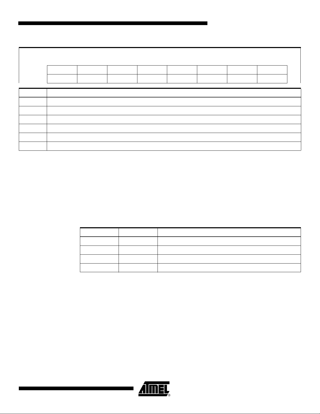
Table 6-1. AT89LP2052/LP4052 SFR Map and Reset Values
0F8H 0FFH
0F0H B*
0000 0000
0E8H 0EFH
0E0H ACC*
0000 0000
0D8H 0DFH
0D0H PSW*
0000 0000
0C8H 0CFH
0C0H P1M0
1111 1111
0B8H IP*
x0x0 0000
0B0H P3*
1111 1111
0A8H IE*
00x0 0000
0A0H WDTRST
SADEN
0000 0000
SADDR
0000 0000
SPSR
000x xx00
P1M1
0000 0000
SPCR
0000 0000
P3M0
1111 1111
(write-only)
P3M1
0000 0000
IPH
x0x0 0000
WDTCON
0000 x000
0F7H
0E7H
0D7H
0C7H
0BFH
0B7H
0AFH
0A7H
98H SCON*
0000 0000
90H P1*
1111 1111
88H TCON*
0000 0000
80H SP
Note: *These SFRs are bit-addressable.
6
AT89LP2052/LP4052
SBUF
xxxx xxxx
TCONB
0010 0100
TMOD
0000 0000
0000 0111
0000 0000
0000 0000
0000 0000
RL0
TL0
DPL
RL1
0000 0000
TL1
0000 0000
DPH
0000 0000
RH0
0000 0000
TH0
0000 0000
RH1
0000 0000
TH1
0000 0000
SPDR
xxxx xxxx
ACSR
xx00 0000
PCON
000x 0000
3547H–MICRO–5/07
9FH
97H
8FH
87H

7. Comparison to Standard 8051
The AT89LP2052/LP4052 is part of a family of devices with enhanced features that are fully
binary compatible with the MCS-51 instruction set. In addition, most SFR addresses, bit assignments, and pin alternate functions are identical to Atmel's existing standard 8051 products.
However, due to the high performance nature of the device, some system behaviors are different from those of Atmel's standard 8051 products such as AT89S52 or AT89S2051. The
differences from the standard 8051 are outlined in the following paragraphs.
7.1 System Clock
The CPU clock frequency equals the external XTAL1 frequency. The oscillator is no longer
divided by 2 to provide the internal clock, and x2 mode is not supported.
7.2 Instruction Execution with Single-cycle Fetch
The CPU fetches one code byte from memory every clock cycle instead of every six clock
cycles. This greatly increases the throughput of the CPU. As a consequence, the CPU no longer
executes instructions in 12 to 48 clock cycles. Each instruction executes in only 1 to 4 clock
cycles. See Section 22. “Instruction Set Summary” on page 51 for more details.
7.3 Interrupt Handling
The interrupt controller polls the interrupt flags during the last clock cycle of any instruction. In
order for an interrupt to be serviced at the end of an instruction, its flag needs to have been
latched as active during the next to last clock cycle of the instruction, or in the last clock cycle of
the previous instruction if the current instruction executes in only a single clock cycle.
AT89LP2052/LP4052
7.4 Timer/Counters
The Timer/Counters increment at a rate of once per clock cycle. This compares to once every
12 clocks in the standard 8051.
7.5 Serial Port
The baud rate of the UART in Mode 0 is 1/2 the clock frequency, compared to 1/12 the clock frequency in the standard 8051. In should also be noted that when using Timer 1 to generate the
baud rate in Mode 1 or Mode 3, the timer counts at the clock frequency and not at 1/12 the clock
frequency. To maintain the same baud rate in the AT89LP2052/LP4052 while running at the
same frequency as a standard 8051, the time-out period must be 12 times longer. Mode 1 of
Timer 1 supports 16-bit auto-reload to facilitate longer time-out periods for generating low baud
rates.
7.6 Watchdog Timer
The Watchdog Timer in AT89LP2052/LP4052 counts at a rate of once per clock cycle. This
compares to once every 12 clocks in the standard 8051.
3547H–MICRO–5/07
7
7.7 I/O Ports
The I/O ports of the AT89LP2052/LP4052 may be configured in four different modes. On the
AT89LP2052/LP4052, all the I/O ports revert to input-only (tri-stated) mode at power-up or reset.
In the standard 8051, all ports are weakly pulled high during power-up or reset. To enable 8051like ports, the ports must be put into quasi-bidirectional mode by clearing the P1M0 and P3M0
SFRs.
7.8 Reset
The RST pin in the AT89LP2052/LP4052 has different pulse width requirements than the standard 8051. The RST pin is sampled every clock cycle and must be held high for a minimum of
two clock cycles, instead of 24 clock cycles, to be recognized as a valid reset pulse
8. Enhanced CPU
The AT89LP2052/LP4052 uses an enhanced 8051 CPU that runs at 6 to 12 times the speed of
standard 8051 devices (or 3 to 6 times the speed of X2-mode 8051 devices). The increase in
performance is due to two factors. First, the CPU fetches one instruction byte from the code
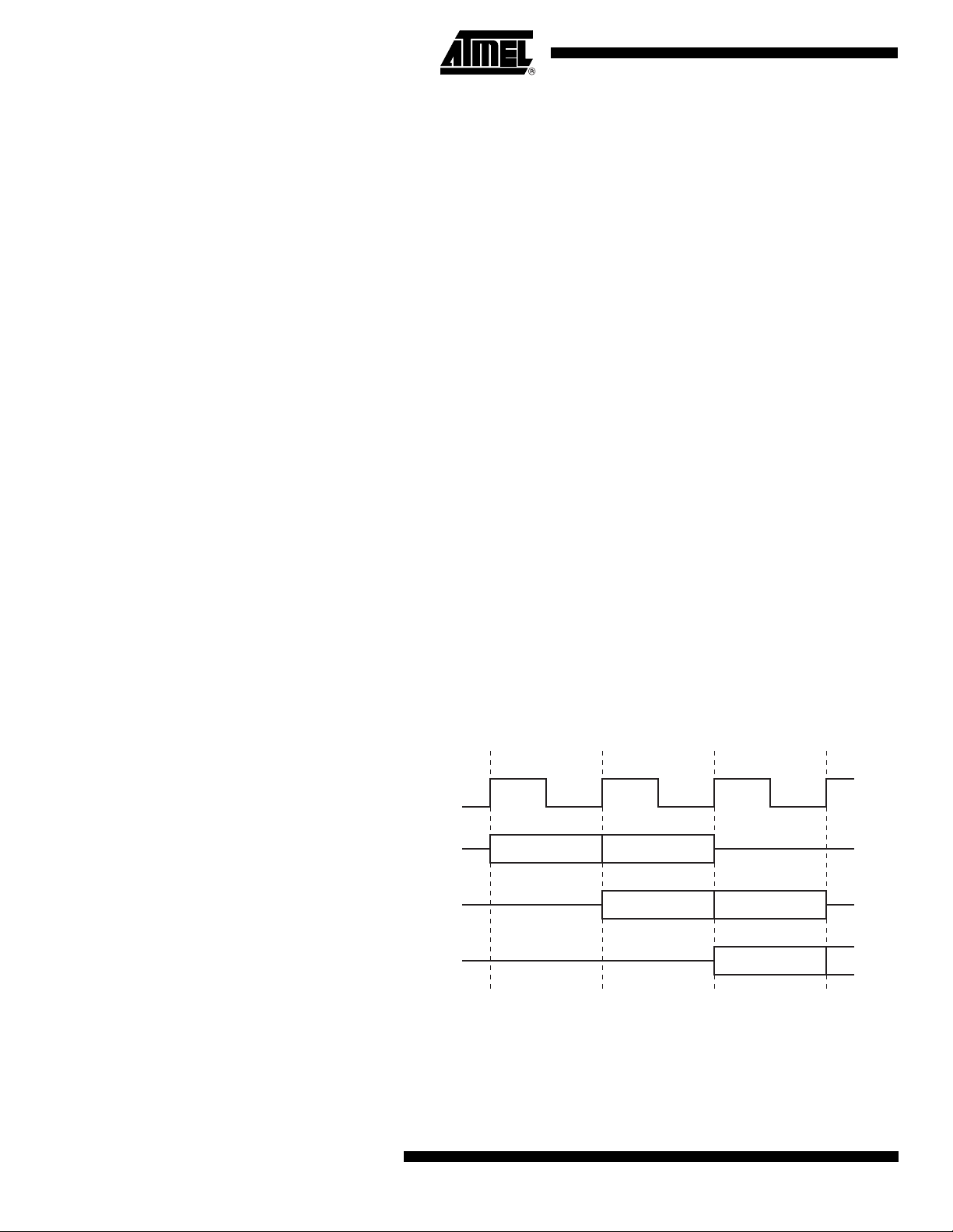
memory every clock cycle. Second, the CPU uses a simple two-stage pipeline to fetch and execute instructions in parallel. This basic pipelining concept allows the CPU to obtain up to 1 MIPS
per MHz. A simple example is shown in Figure 8-1.
The MCS-51 instruction set allows for instructions of variable length from 1 to 3 bytes. In a single-clock-per-byte-fetch system this means each instruction takes at least as many clocks as it
has bytes to execute. A majority of the instructions in the AT89LP2052/LP4052 follow this rule:
the instruction execution time in clock cycles equals the number of bytes per instruction with a
few exceptions. Branches and Calls require an additional cycle to compute the target address
and some other complex instructions require multiple cycles. See Section 22. “Instruction Set
Summary” on page 51 for more detailed information on individual instructions. Figures 8-2 and
8-3 show examples of one- and two-byte instructions.
Figure 8-1. Parallel Instruction Fetches and Executions
T
n
System Clock
th
n
Instruction
th
(n+1)
(n+2)th Instruction
8
AT89LP2052/LP4052
Instruction
Fetch Execute
T
n+1
Fetch Execute
T
n+2
Fetch
3547H–MICRO–5/07
AT89LP2052/LP4052
Figure 8-2. Single-cycle ALU Operation (Example: INC R0)
T
1
System Clock
Total Execution Time
Register Operand Fetch
ALU Operation Execute
Result Write Back
Fetch Next Instruction
Figure 8-3. Two-Cycle ALU Operation (Example: ADD A,
T
1
System Clock
Total Execution Time
T
2
#data
T
2
T
3
)
T
3
Fetch Immediate Operand
ALU Operation Execute
Result Write Back
Fetch Next Instruction
3547H–MICRO–5/07
9

9. Restrictions on Certain Instructions
The AT89LP2052/LP4052 is an economical and cost-effective member of Atmel's growing family of microcontrollers. It contains 2/4K bytes of Flash program memory. It is fully compatible with
the MCS-51 architecture, and can be programmed using the MCS-51 instruction set. However,
there are a few considerations one must keep in mind when utilizing certain instructions to program this device. All the instructions related to jumping or branching should be restricted such
that the destination address falls within the physical program memory space of the device, which
is 2K bytes for the AT89LP2052 and 4K bytes for the AT89LP4052. This should be the responsibility of the software programmer. For example, LJMP 7E0H would be a valid instruction for the
AT89LP2052 (with 2K bytes of memory), whereas LJMP 900H would not.
9.1 Branching Instructions
The LCALL, LJMP, ACALL, AJMP, SJMP, and JMP @A+DPTR unconditional branching instructions will execute correctly as long as the programmer keeps in mind that the destination
branching address must fall within the physical boundaries of the program memory size (locations 000H to 7FFH for the AT89LP2052, 000H to FFFH for the AT89LP4052). Violating the
physical space limits may cause unknown program behavior. With the CJNE [...], DJNZ [...], JB,
JNB, JC, JNC, JBC, JZ, and JNZ conditional branching instructions, the same previous rule
applies. Again, violating the memory boundaries may cause erratic execution. For applications
involving interrupts, the normal interrupt service routine address locations of the 8051 family
architecture have been preserved.
9.2 MOVX-related Instructions, Data Memory
External DATA memory access is not supported in this device, nor is external PROGRAM memory execution. Therefore, no MOVX [...] instructions should be included in the program. A typical
8051 assembler will still assemble instructions, even if they are written in violation of the restrictions mentioned above. It is the responsibility of the user to know the physical features and
limitations of the device being used and to adjust the instructions used accordingly.
10. System Clock
The system clock is generated directly from one of two selectable clock sources. The two
sources are the on-chip crystal oscillator and external clock source. No internal clock division is
used to generate the CPU clock from the system clock.
10.1 Crystal Oscillator
When enabled, the internal inverting oscillator amplifier is connected between XTAL1 and
XTAL2 for connection to an external quartz crystal or ceramic resonator. When using the crystal
oscillator, XTAL2 should not be used to drive a board-level clock.
10.2 External Clock Source
The external clock option is selected by setting the Oscillator Bypass fuse. This disables the
amplifier and allows XTAL1 to be driven directly by the clock source. XTAL2 may be left
unconnected.
10.3 System Clock Out
When the System Clock Out fuse is enabled, P3.7 will output the system clock with no division
using the push-pull output mode. During Power-down the system clock will output as “1”.
10
AT89LP2052/LP4052
3547H–MICRO–5/07
11. Oscillator Characteristics
XTAL1 and XTAL2 are the input and output, respectively, of an inverting amplifier that can be
configured for use as an on-chip oscillator, as shown in Figure 11-1. Either a quartz crystal or
ceramic resonator may be used. Figures 11-2 and 11-3 illustrate the relationship between sam-
ple clock loading and the respective resulting clock amplitudes.
Figure 11-1. Oscillator Connections
AT89LP2052/LP4052
Note: C1, C2 = 5 pF ± 5 pF for Crystals
= 5 pF ± 5 pF for Ceramic Resonators
Figure 11-2. Quartz Crystal Clock Source
Quartz Crystal Clock Input
6.5
6
5.5
5
4.5
4
3.5
3
2.5
Xtal1 Amplitude (V)
2
1.5
1
2 4 6 8 10 12 14 16 18 20 22 24
Frequency (MHz)
0 pF
5 pF
10 pF
3547H–MICRO–5/07
11
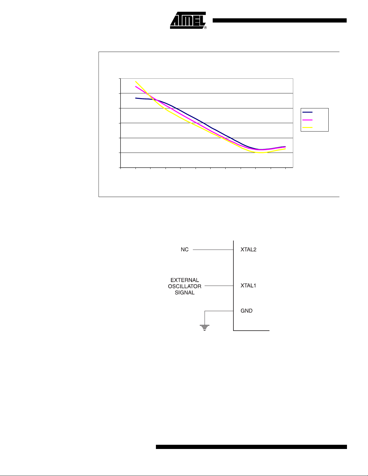
Figure 11-3. Ceramic Resonator Clock Source
Ceramic Resonator Clock Input
6
5
4
3
2
Xtal1 Amplitude (V)
1
0
2 4 6 8 10 12 14 16 18 20 22 24
Frequency (MHz)
0 pF
5 pF
10 pF
To drive the device from an external clock source, XTAL2 should be left unconnected while
XTAL1 is driven, as shown in Figure 11-4.
Figure 11-4. External Clock Drive Configuration
12
AT89LP2052/LP4052
3547H–MICRO–5/07

12. Reset
During reset, all I/O Registers are set to their initial values, the port pins are tri-stated, and the
program starts execution from the Reset Vector, 0000H. The AT89LP2052/LP4052 has four
sources of reset: power-on reset, brown-out reset, external reset, and watchdog reset.
12.1 Power-on Reset
A Power-on Reset (POR) is generated by an on-chip detection circuit. The detection level is
nominally 1.4V. The POR is activated whenever V
cuit can be used to trigger the start-up reset or to detect a supply voltage failure in devices
without a brown-out detector. The POR circuit ensures that the device is reset from power-on.
When V
how long the device is kept in POR after V
any delay, when V
will set the POF flag in PCON.
12.2 Brown-out Reset
The AT89LP2052/LP4052 has an on-chip Brown-out Detection (BOD) circuit for monitoring the
V
nominally 2.2V. The purpose of the BOD is to ensure that if V
speed, the system will gracefully enter reset without the possibility of errors induced by incorrect
execution. When V
diately activated. When V
MCU after the time-out period has expired.
AT89LP2052/LP4052
is below the detection level. The POR cir-
CC
reaches the Power-on Reset threshold voltage, the POR delay counter determines
CC
rise. The POR signal is activated again, without
CC
falls below the POR threshold level. A Power-on Reset (i.e. a cold reset)
CC
level during operation by comparing it to a fixed trigger level. The trigger level for the BOD is
CC
fails or dips while executing at
CC
decreases to a value below the trigger level, the Brown-out Reset is imme-
CC
increases above the trigger level, the BOD delay counter starts the
CC
12.3 External Reset
The RST pin functions as an active-high reset input. The pin must be held high for at least two
clock cycles to trigger the internal reset. RST also serves as the In-System Programming (ISP)
enable. ISP is enabled when the external reset pin is held high and the ISP Enable fuse is
enabled.
12.4 Watchdog Reset
When the Watchdog times out, it will generate an internal reset pulse lasting 16 clock cycles.
Watchdog reset will also set the WDTOVF flag in WDTCON. To prevent a Watchdog reset, the
watchdog reset sequence 1EH/E1H must be written to WDTRST before the Watchdog times
out. A Watchdog reset will occur only if the Watchdog has been enabled. The Watchdog is disabled by default after any reset and must always be re-enabled if needed.
13. Power Saving Modes
The AT89LP2052/LP4052 supports two different power-reducing modes: Idle and Power-down.
These modes are accessed through the PCON register.
3547H–MICRO–5/07
13

13.1 Idle Mode
Setting the IDL bit in PCON enters Idle mode. Idle mode halts the internal CPU clock. The CPU
state is preserved in its entirety, including the RAM, stack pointer, program counter, program
status word, and accumulator. The Port pins hold the logic states they had at the time that Idle
was activated. Idle mode leaves the peripherals running in order to allow them to wake up the
CPU when an interrupt is generated. The Timer, UART and SPI blocks continue to function during Idle. The comparator and watchdog may be selectively enabled or disabled during Idle. Any
enabled interrupt source or reset may terminate Idle mode. When exiting Idle mode with an interrupt, the interrupt will immediately be serviced, and following RETI the next instruction to be
executed will be the one following the instruction that put the device into Idle.
13.2 Power-down Mode
Setting the Power-down (PD) bit in PCON enters Power-down mode. Power-down mode stops
the oscillator and powers down the Flash memory in order to minimize power consumption. Only
the power-on circuitry will continue to draw power during Power-down. During Power-down, the
power supply voltage may be reduced to the RAM keep-alive voltage. The RAM contents will be
retained, but the SFR contents are not guaranteed once V
may be exited by external reset, power-on reset, or certain interrupts.
The user should not attempt to enter (or re-enter) the power-down mode for a minimum of 4 µs
until after one of the following conditions has occurred: Start of code execution (after any type of
reset), or Exit from power-down mode.
has been reduced. Power-down
CC
13.2.1 Interrupt Recovery from Power-down
Two external interrupts may be configured to terminate Power-down mode. Pins P3.2 and P3.3
may be used to exit Power-down through external interrupts INT0
external interrupts INT0
tive operation. If configured as inputs, INT0
down even if interrupt recovery is not used.
When terminating Power-down by an interrupt, two different wake-up modes are available.
When PWDEX in PCON is zero, the wake-up period is internally timed. At the falling edge on the
interrupt pin, Power-down is exited, the oscillator is restarted, and an internal timer begins counting. The internal clock will not be allowed to propagate to the CPU until after the timer has
counted for nominally 2 ms. After the time-out period the interrupt service routine will begin. The
interrupt pin may be held low until the device has timed out and begun executing, or it may
return high before the end of the time-out period. If the pin remains low, the service routine
should disable the interrupt before returning to avoid re-triggering the interrupt.
When PWDEX = “1”, the wake-up period is controlled externally by the interrupt. Again, at the
falling edge on the interrupt pin, Power-down is exited and the oscillator is restarted. However,
the internal clock will not propagate until the rising edge of the interrupt pin. The interrupt should
be held low long enough for the selected clock source to stabilize.
13.2.2 Reset Exit from Power-down
The wake-up from Power-down through an external reset is similar to the interrupt with
PWDEX = “0”. At the rising edge of RST, Power-down is exited, the oscillator is restarted, and
an internal timer begins counting. The internal clock will not be allowed to propagate to the CPU
until after the timer has counted for nominally 2 ms. The RST pin must be held high for longer
than the time-out period to ensure that the device is reset properly. The device will begin executing once RST is brought back low.
and INT1. To wake up by
or INT1, that interrupt must be enabled and configured for level-sensi-
and INT1 should not be left floating during Power-
14
AT89LP2052/LP4052
3547H–MICRO–5/07

AT89LP2052/LP4052
Table 13-1.
PCON = 87H Reset Value = 000X 0000B
Not Bit Addressable
Bit76543210
Symbol Function
SMOD1 Double Baud Rate bit. Doubles the baud rate of the UART in Modes 1, 2, or 3.
SMOD0 Frame Error Select. When SMOD0 = 1, SCON.7 is SM0. When SMOD0 = 1, SCON.7 is FE. Note that FE will be set after
PWDEX Power-down Exit Mode. When PWDEX = 1, wake up from Power-down is externally controlled. When PWDEX = 0, wake
POF Power Off Flag. POF is set to “1” during power up (i.e. cold reset). It can be set or reset under software control and is not
GF1, GF0 General-purpose Flags
PD Power-down bit. Setting this bit activates power-down operation.
IDL Idle Mode bit. Setting this bit activates Idle mode operation
PCON
– Power Control Register
SMOD1 SMOD0 PWDEX POF GF1 GF0 PD IDL
a frame error regardless of the state of SMOD0.
up from Power-down is internally timed.
affected by RST or BOD (i.e. warm resets).
14. Interrupts
The AT89LP2052/LP4052 provides 6 interrupt sources: two external interrupts, two timer interrupts, a serial port interrupt, and an analog comparator interrupt. These interrupts and the
system reset each have a separate program vector at the start of the program memory space.
Each interrupt source can be individually enabled or disabled by setting or clearing a bit in the
interrupt enable register IE. The IE register also contains a global disable bit, EA, which disables
all interrupts.
3547H–MICRO–5/07
Each interrupt source can be individually programmed to one of four priority levels by setting or
clearing bits in the interrupt priority registers IP and IPH. An interrupt service routine in progress
can be interrupted by a higher priority interrupt, but not by another interrupt of the same or lower
priority. The highest priority interrupt cannot be interrupted by any other interrupt source. If two
requests of different priority levels are pending at the end of an instruction, the request of higher
priority level is serviced. If requests of the same priority level are pending at the end of an
instruction, an internal polling sequence determines which request is serviced. The polling
sequence is based on the vector address; an interrupt with a lower vector address has higher
priority than an interrupt with a higher vector address. Note that the polling sequence is only
used to resolve pending requests of the same priority level.
The External Interrupts INT0
and INT1 can each be either level-activated or edge-activated,
depending on bits IT0 and IT1 in Register TCON. The flags that actually generate these interrupts are the IE0 and IE1 bits in TCON. When the service routine is vectored to, hardware clears
the flag that generated an external interrupt only if the interrupt was edge-activated. If the interrupt was level activated, then the external requesting source (rather than the on-chip hardware)
controls the request flag.
15

The Timer 0 and Timer 1 Interrupts are generated by TF0 and TF1, which are set by a rollover in
their respective Timer/Counter registers (except for Timer 0 in Mode 3). When a timer interrupt is
generated, the on-chip hardware clears the flag that generated it when the service routine is
vectored to.
The Serial Port Interrupt is generated by the logic OR of RI and TI in SCON plus SPIF in SPSR.
None of these flags is cleared by hardware when the service routine is vectored to. In fact, the
service routine normally must determine whether RI, TI, or SPIF generated the interrupt, and the
bit must be cleared by software.
The CF bit in ACSR generates the Comparator Interrupt. The flag is not cleared by hardware
when the service routine is vectored to and must be cleared by software.
Most of the bits that generate interrupts can be set or cleared by software, with the same result
as though they had been set or cleared by hardware. That is, interrupts can be generated and
pending interrupts can be canceled in software. The exception is the SPI interrupt flag SPIF.
This flag is only set by hardware and may only be cleared by software.
Table 14-1. Interrupt Vector Addresses
Interrupt Source Vector Address
System Reset RST or POR or BOD 0000H
External Interrupt 0 IE0 0003H
Timer 0 Overflow TF0 000BH
External Interrupt 1 IE1 0013H
Timer 1 Overflow TF1 001BH
Serial Port RI or TI or SPIF 0023H
Reserved – 002BH
Analog Comparator CF 0033H
14.1 Interrupt Response Time
The interrupt flags may be set by their hardware in any clock cycle. The interrupt controller polls
the flags in the last clock cycle of the instruction in progress. If one of the flags was set in the
preceding cycle, the polling cycle will find it and the interrupt system will generate an LCALL to
the appropriate service routine as the next instruction, provided that the interrupt is not blocked
by any of the following conditions: an interrupt of equal or higher priority level is already in
progress; the instruction in progress is RETI or any write to the IE, IP, or IPH registers. Either of
these conditions will block the generation of the LCALL to the interrupt service routine. The second condition ensures that if the instruction in progress is RETI or any access to IE, IP or IPH,
then at least one more instruction will be executed before any interrupt is vectored to. The polling cycle is repeated at the last cycle of each instruction, and the values polled are the values
that were present at the previous clock cycle. If an active interrupt flag is not being serviced
because of one of the above conditions and is no longer active when the blocking condition is
removed, the denied interrupt will not be serviced. In other words, the fact that the interrupt flag
was once active but not serviced is not remembered. Every polling cycle is new.
16
AT89LP2052/LP4052
3547H–MICRO–5/07
AT89LP2052/LP4052
n
If a request is active and conditions are met for it to be acknowledged, a hardware subroutine
call to the requested service routine will be the next instruction executed. The call itself takes
four cycles. Thus, a minimum of five complete clock cycles elapsed between activation of an
interrupt request and the beginning of execution of the first instruction of the service routine.
A longer response time results if the request is blocked by one of the previously listed conditions. If an interrupt of equal or higher priority level is already in progress, the additional wait time
depends on the nature of the other interrupt's service routine. If the instruction in progress is not
in its final clock cycle, the additional wait time cannot be more than 3 cycles, since the longest
are only 4 cycles long. If the instruction in progress is RETI or an access to IE or IP, the additional wait time cannot be more than 7 cycles (a maximum of three more cycles to complete the
instruction in progress, plus a maximum of 4 cycles to complete the next instruction). Thus, in a
single-interrupt system, the response time is always more than 5 clock cycles and less than
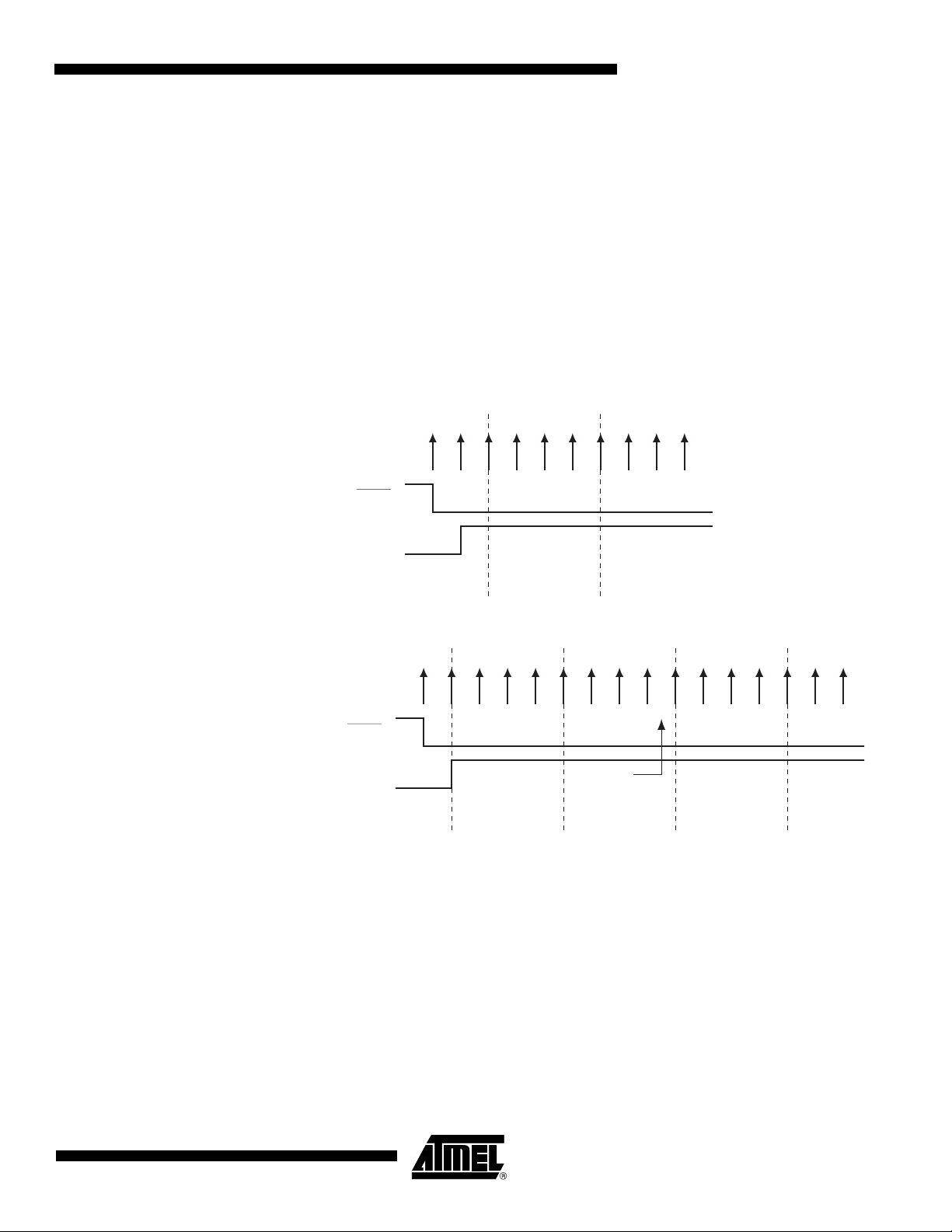
13 clock cycles. See Figures 14-1 and 14-2.
Figure 14-1. Minimum Interrupt Response Time
Clock Cycles
INT0
IE0
Instruction LCALL 1st ISR Instr.Cur. Instr.
Figure 14-2. Maximum Interrupt Response Time
Clock Cycles
INT0
IE0
Instruction RETI 4 Cyc. Instr. LCALL 1st ISR I
15
Ack.
113
Ack.
3547H–MICRO–5/07
17

Table 14-2.
IE = A8H Reset Value = 00X0 0000B
Bit Addressable
Bit76543210
Symbol Function
EA Global enable/disable. All interrupts are disabled when EA = 0. When EA = 1, each interrupt source is enabled/disabled
EC Comparator Interrupt Enable
ES Serial Port Interrupt Enable
ET1 Timer 1 Interrupt Enable
EX1 External Interrupt 1 Enable
ET0 Timer 0 Interrupt Enable
EX0 External Interrupt 0 Enable
IE
– Interrupt Enable Register
EA EC – ES ET1 EX1 ET0 EX0
by setting /clearing its own enable bit.
Table 14-3.
IP = B8H Reset Value = X0X0 0000B
Bit Addressable
Bit76543210
Symbol Function
PC Comparator Interrupt Priority Low
PS Serial Port Interrupt Priority Low
PT1 Timer 1 Interrupt Priority Low
PX1 External Interrupt 1 Priority Low
PT0 Timer 0 Interrupt Priority Low
PX0 External Interrupt 0 Priority Low
IP
– Interrupt Priority Register
–
PC – PS PT1 PX1 PT0 PX0
18
AT89LP2052/LP4052
3547H–MICRO–5/07
AT89LP2052/LP4052
Table 14-4.
IPH = B7H Reset Value = X0X0 0000B
Not Bit Addressable
Bit76543210
Symbol Function
PCH Comparator Interrupt Priority High
PSH Serial Port Interrupt Priority High
PT1H Timer 1 Interrupt Priority High
PX1H External Interrupt 1 Priority High
PT0H Timer 0 Interrupt Priority High
PX0H External Interrupt 0 Priority High
IPH
– Interrupt Priority High Register
–
PCH – PSH PT1H PX1H PT0H PX0H
15. I/O Ports
All 15 port pins on the AT89LP2052/LP4052 may be configured to one of four modes: quasi-bidirectional (standard 8051 port outputs), push-pull output, open-drain output, or input-only. Port
modes may be assigned in software on a pin-by-pin basis as shown in Table 15-1. All port pins
default to input-only mode after reset. Each port pin also has a Schmitt-triggered input for
improved input noise rejection. During Power-down all the Schmitt-triggered inputs are disabled
with the exception of P3.2 and P3.3, which may be used to wake-up the device. Therefore P3.2
and P3.3 should not be left floating during Power-down.
Table 15-1. Configuration Modes for Port x, Bit y
PxM0.y PxM1.y Port Mode
0 0 Quasi-bidirectional
0 1 Push-pull Output
1 0 Input Only (High Impedance)
1 1 Open-Drain Output
15.1 Quasi-bidirectional Output
Port pins in quasi-bidirectional output mode function similar to standard 8051 port pins. A Quasibidirectional port can be used both as an input and output without the need to reconfigure the
port. This is possible because when the port outputs a logic high, it is weakly driven, allowing an
external device to pull the pin low. When the pin is driven low, it is driven strongly and able to
sink a large current. There are three pull-up transistors in the quasi-bidirectional output that
serve different purposes.
One of these pull-ups, called the “very weak” pull-up, is turned on whenever the port register for
the pin contains a logic “1”. This very weak pull-up sources a very small current that will pull the
pin high if it is left floating.
3547H–MICRO–5/07
19
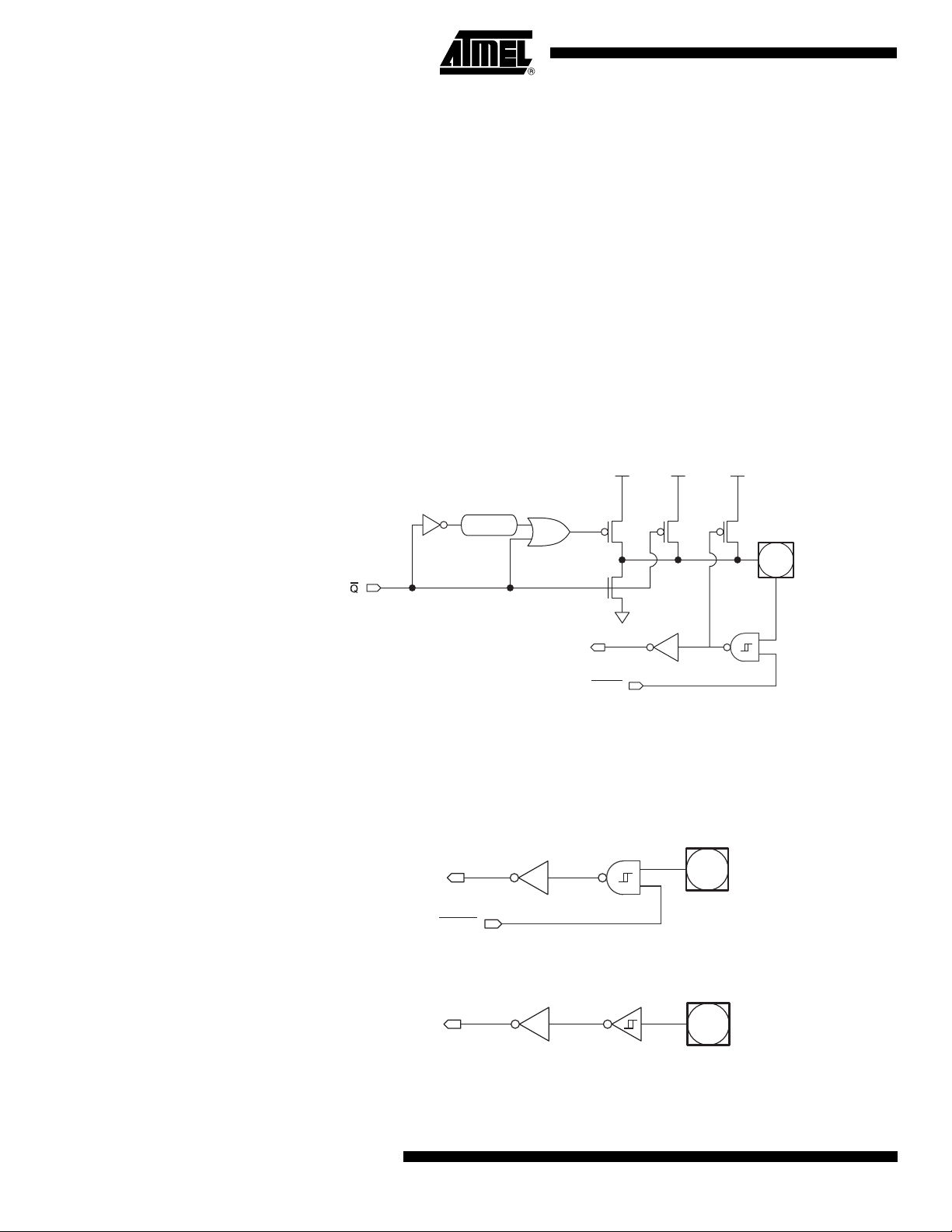
A second pull-up, called the “weak” pull-up, is turned on when the port register for the pin contains a logic “1” and the pin itself is also at a logic “1” level. This pull-up provides the primary
source current for a quasi-bidirectional pin that is outputting a 1. If this pin is pulled low by an
external device, this weak pull-up turns off, and only the very weak pull-up remains on. In order
to pull the pin low under these conditions, the external device has to sink enough current to overpower the weak pull-up and pull the port pin below its input threshold voltage.
The third pull-up is referred to as the “strong” pull-up. This pull-up is used to speed up low-tohigh transitions on a quasi-bidirectional port pin when the port register changes from a logic “0”
to a logic “1”. When this occurs, the strong pull-up turns on for one CPU clock, quickly pulling the
port pin high.
When in quasi-bidirectional mode the port pin will always output a “0” when corresponding bit in
the port register is also “0”. When the port register is “1” the pin may be used either as an input
or an output of “1”. The quasi-bidirectional port configuration is shown in Figure 15-1. The input
circuitry of P3.2 and P3.3 is not disabled during Power-down (see Figure 15-3).
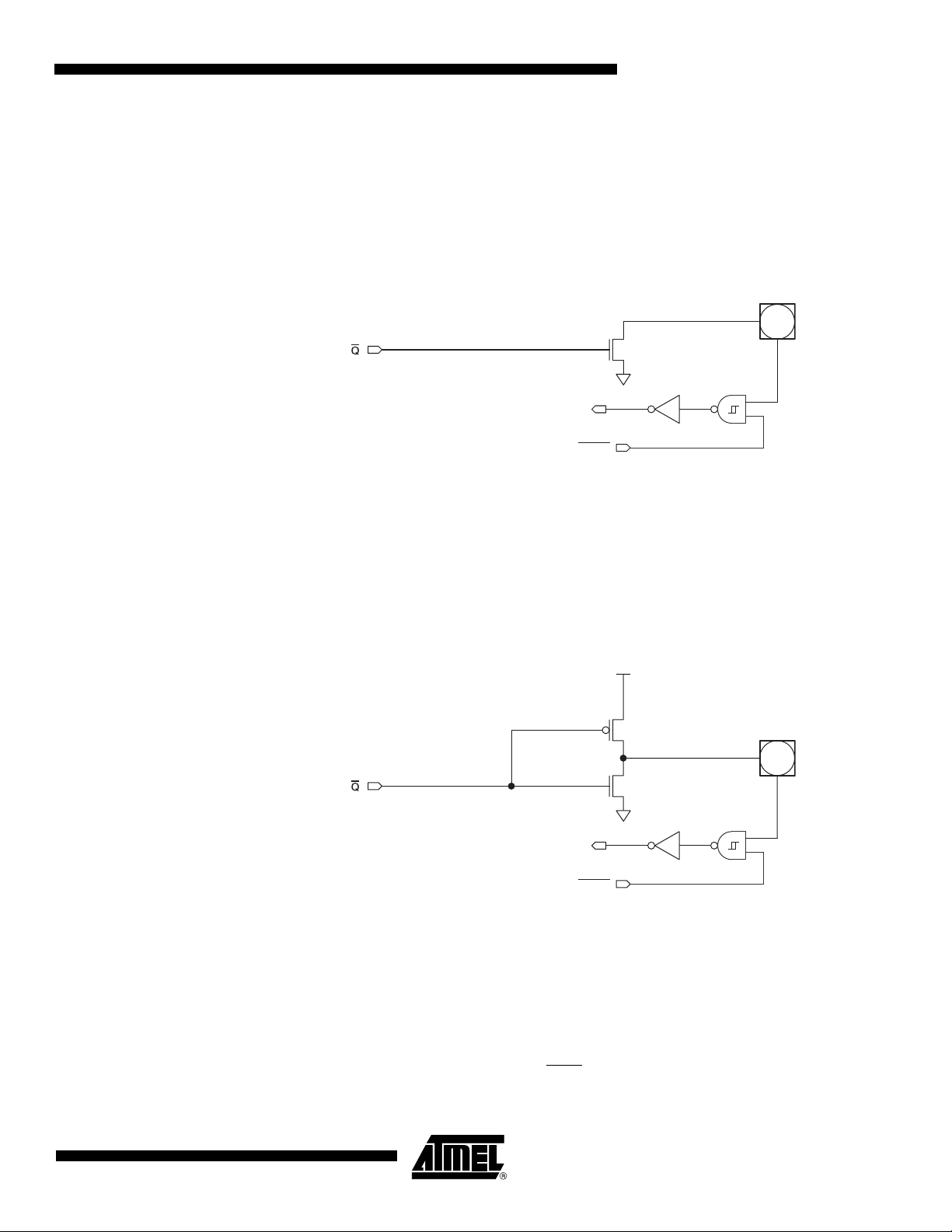
Figure 15-1. Quasi-bidirectional Output
15.2 Input-only Mode
The input port configuration is shown in Figure 15-2. It is a Schmitt-triggered input for improved
input noise rejection.
Figure 15-2. Input Only
From Port
Register
Input
Data
1 Clock Delay
(D Flip-Flop)
Input
Data
PWD
V
CC
Strong
V
CC
Ver y
Weak
Por t
Pin
V
CC
Weak
Por t
Pin
20
Figure 15-3. Input Only for P3.2 and P3.3
AT89LP2052/LP4052
Input
Data
PWD
Por t
Pin
3547H–MICRO–5/07
15.3 Open-drain Output
The open-drain output configuration turns off all pull-ups and only drives the pull-down transistor
of the port pin when the port register contains a logic “0”. To be used as a logic output, a port
configured in this manner must have an external pull-up, typically a resistor tied to V
down for this mode is the same as for the quasi-bidirectional mode. The open-drain port configuration is shown in Figure 15-4. The input circuitry of P3.2 and P3.3 is not disabled during Powerdown (see Figure 15-3).
Figure 15-4. Open-Drain Output
15.4 Push-pull Output
The push-pull output configuration has the same pull-down structure as both the open-drain and
the quasi-bidirectional output modes, but provides a continuous strong pull-up when the port
register contains a logic “1”. The push-pull mode may be used when more source current is
needed from a port output. The push-pull port configuration is shown in Figure 15-5. The input
circuitry of P3.2 and P3.3 is not disabled during Power-down (see Figure 15-3).
From Port
Register
Input
Data
PWD
AT89LP2052/LP4052
. The pull-
CC
Por t
Pin
Figure 15-5. Push-pull Output
15.5 Port 1 Analog Functions
The AT89LP2052/LP4052 incorporates an analog comparator. In order to give the best analog
performance and minimize power consumption, pins that are being used for analog functions
must have both the digital outputs and digital inputs disabled. Digital outputs are disabled by putting the port pins into the input-only mode as described in Section 15. “I/O Ports” on page 19.
Digital inputs on P1.0 and P1.1 are disabled whenever the Analog Comparator is enabled by
setting the CEN bit in ACSR. CEN forces the PWD
the Schmitt trigger circuitry.
From Port
Register
V
CC
Por t
Pin
Input
Data
PWD
input on P1.0 and P1.1 low, thereby disabling
3547H–MICRO–5/07
21

15.6 Port Read-Modify-Write
A read from a port will read either the state of the pins or the state of the port register depending
on which instruction is used. Simple read instructions will always access the port pins directly.
Read-modify-write instructions, which read a value, possibly modify it, and then write it back, will
always access the port register. This includes bit write instructions such as CLR or SETB as they
actually read the entire port, modify a single bit, then write the data back to the entire port. See
Table 15-2 for a complete list of Read-Modify-Write instruction which may access the ports.
Table 15-2. Port Read-Modify-Write Instructions
Mnemonic Instruction Example
ANL Logical AND ANL P1, A
ORL Logical OR ORL P1, A
XRL Logical EX-OR XRL P1, A
JBC Jump if bit set and clear bit JBC P3.0, LABEL
CPL Complement bit CPL P3.1
INC Increment INC P1
DEC Decrement DEC P3
DJNZ Decrement and jump if not zero DJNZ P3, LABEL
MOV PX.Y, C Move carry to bit Y of Port X MOV P1.0, C
CLR PX.Y Clear bit Y of Port X CLR P1.1
SETB PX.Y Set bit Y of Port X SETB P3.2
15.7 Port Alternate Functions
Most general-purpose digital I/O pins of the AT89LP2052/LP4052 share functionality with the
various I/Os needed for the peripheral units. Table 15-4 lists the alternate functions of the port
pins. Alternate functions are connected to the pins in a logic AND fashion. In order to enable the
alternate function on a port pin, that pin must have a “1” in its corresponding port register bit, otherwise, the input/output will always be “0”. Furthermore, each pin must be configured
for the correct input/output mode as required by its peripheral before it may be used as such.
Table 15-3 shows how to configure a generic pin for use with an alternate function.
Table 15-3. Alternate Function Configurations for Pin y of Port x
PxM0.y PxM1.y Px.y I/O Mode
0 0 1 Bidirectional (internal pull-up)
011Output
1 0 X Input
1 1 1 Bidirectional (external pull-up)
22
AT89LP2052/LP4052
3547H–MICRO–5/07

Table 15-4. Port Pin Alternate Functions
AT89LP2052/LP4052
Port
Pin
P1.0 P1M0.0 P1M1.0 AIN0 Input-only
P1.1 P1M0.1 P1M1.1 AIN1 Input-only
P1.4 P1M0.4 P1M1.4 SS
P1.5 P1M0.5 P1M1.5 MOSI
P1.6 P1M0.6 P1M1.6 MISO
P1.7 P1M0.7 P1M1.7 SCK
P3.0 P3M0.0 P3M1.0 RXD
P3.1 P3M0.1 P3M1.1 TXD
P3.2 P3M0.2 P3M1.2 INT0
P3.3 P3M0.3 P3M1.3 INT1
P3.4 P3M0.4 P3M1.4 T0
P3.5 P3M0.5 P3M1.5 T1
P3.6 Not configurable CMPOUT Pin is tied to comparator output
16. Enhanced Timer/Counters
The AT89LP2052/LP4052 has two 16-bit Timer/Counter registers: Timer 0 and Timer 1. As a
Timer, the register is incremented every clock cycle. Thus, the register counts clock cycles.
Since a clock cycle consists of one oscillator period, the count rate is equal to the oscillator
frequency.
Configuration Bits
Alternate
Function NotesPxM0.y PxM1.y
Refer to Section 19.4 “SPI Pin
Configuration” on page 47
Refer to Section 16.6 “Timer/Counter Pin
Configuration” on page 29
16.1 Mode 0
As a Counter, the register is incremented in response to a 1-to-0 transition at its corresponding
input pin, T0 or T1. The external input is sampled every clock cycle. When the samples show a
high in one cycle and a low in the next cycle, the count is incremented. The new count value
appears in the register during the cycle following the one in which the transition was detected.
Since 2 clock cycles are required to recognize a 1-to-0 transition, the maximum count rate is 1/2
of the oscillator frequency. There are no restrictions on the duty cycle of the input signal, but it
should be held for at least one full clock cycle to ensure that a given level is sampled at least
once before it changes.
Furthermore, the Timer or Counter functions for Timer 0 and Timer 1 have four operating modes:
variable width timer/counter, 16 bit auto-reload timer/counter, 8 bit auto-reload timer/counter,
and split timer/counter. The control bits C/T
in the Special Function Register TMOD select the
Timer or Counter function. The bit pairs (M1, M0) in TMOD select the operating modes.
Both Timers in Mode 0 are 8-bit Counters with a variable prescaler. The prescaler may vary from
1 to 8 bits depending on the PSC bits in TCONB, giving the timer a range of 9 to 16 bits.
By default the timer is configured as a 13-bit timer compatible to Mode 0 in the standard 8051.
Figure 16-1 shows the Mode 0 operation as it applies to Timer 1 in 13-bit mode. As the count
rolls over from all “1”s to all “0”s, it sets the Timer interrupt flag TF1. The counted input is
enabled to the Timer when TR1 = 1 and either GATE = 0 or INT1
the Timer to be controlled by external input INT1
, to facilitate pulse width measurements. TR1 is
= 1. Setting GATE = 1 allows
3547H–MICRO–5/07
23
a control bit in the Special Function Register TCON. GATE is in TMOD. The 13-bit register consists of all 8 bits of TH1 and the lower 5 bits of TL1. The upper 3 bits of TL1 are indeterminate
and should be ignored. Setting the run flag (TR1) does not clear the registers. See Figure 16-1.
Figure 16-1. Timer/Counter 1 Mode 0: Variable Width Counter
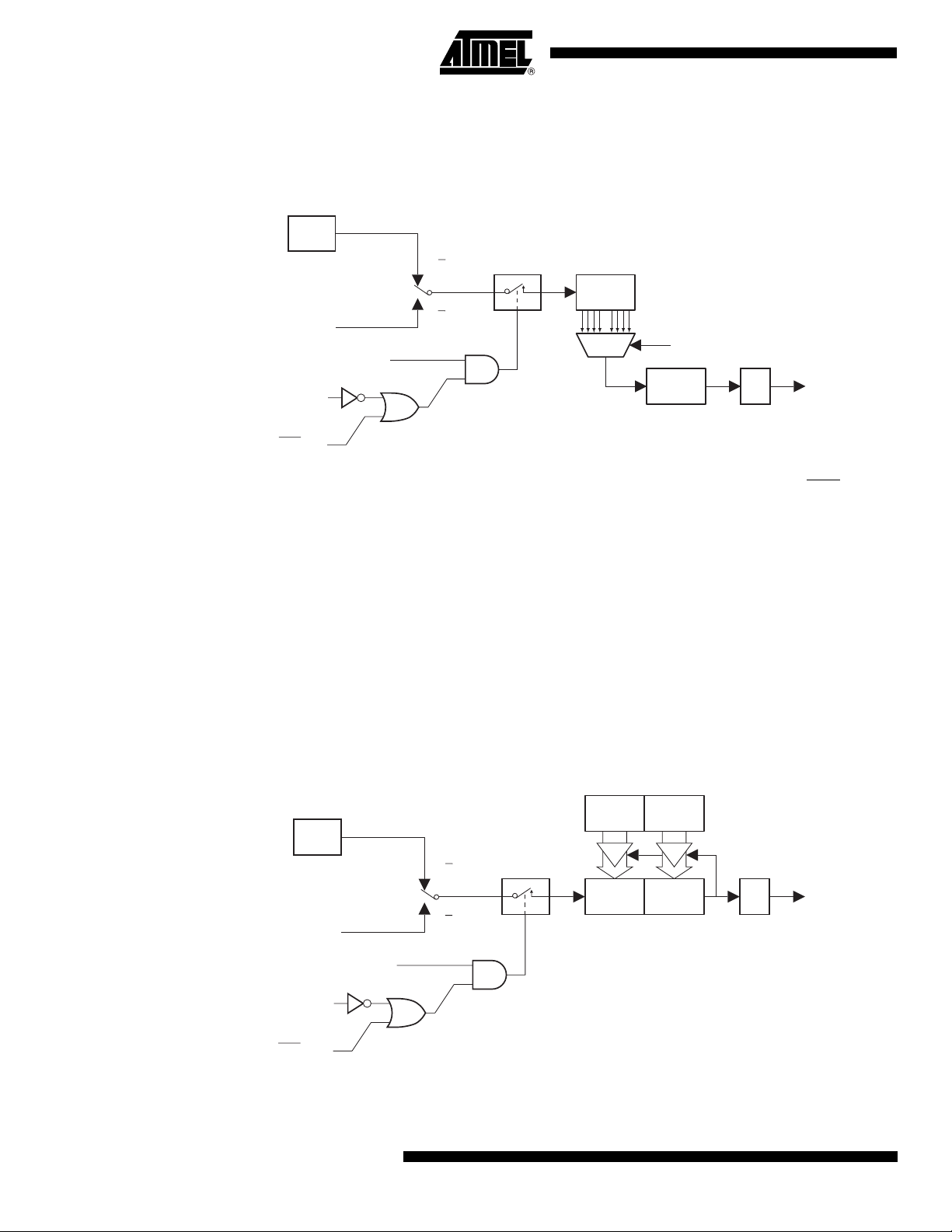
OSC
C/T = 0
TL1
(8 Bits)
T1 Pin
TR1
GATE
INT1 Pin
C/T = 1
Control
PSC1
TH1
(8 Bits)
TF1
Interrupt
16.2 Mode 1
Mode 0 operation is the same for Timer 0 as for Timer 1, except that TR0, TF0 and INT0
replace
the corresponding Timer 1 signals in Figure 16-1. There are two different GATE bits, one for
Timer 1 (TMOD.7) and one for Timer 0 (TMOD.3).
In Mode 1 the Timers are configured for 16-bit auto-reload. The Timer register is run with all 16
bits. The 16-bit reload value is stored in the high and low reload registers (RH1/RL1). The clock
is applied to the combined high and low timer registers (TH1/TL1). As clock pulses are received,
the timer counts up: 0000H, 0001H, 0002H, etc. An overflow occurs on the FFFFH-to-0000H
transition, upon which the timer register is reloaded with the value from RH1/RL1 and the overflow flag bit in TCON is set. See Figure 16-2. The reload registers default to 0000H, which gives
the full 16-bit timer period compatible with the standard 8051. Mode 1 operation is the same for
Timer/Counter 0.
Figure 16-2. Timer/Counter 1 Mode 1: 16-bit Auto-Reload
OSC
T1 Pin
C/T = 0
C/T =1
RL1
(8 Bits)
TL1
(8 Bits)
Control
RH1
(8 Bits)
TH1
(8 Bits)
Reload
TF1
Interrupt
24
TR1
GATE
INT1 Pin
AT89LP2052/LP4052
3547H–MICRO–5/07
16.3 Mode 2
AT89LP2052/LP4052
Mode 2 configures the Timer register as an 8-bit Counter (TL1) with automatic reload, as shown
in Figure 16-3. Overflow from TL1 not only sets TF1, but also reloads TL1 with the contents of
TH1, which is preset by software. The reload leaves TH1 unchanged. Mode 2 operation is the
same for Timer/Counter 0.
Figure 16-3. Timer/Counter 1 Mode 2: 8-bit Auto-Reload
OSC
C/T = 0
T1 Pin
GATE
INT0 Pin
TR1
C/T = 1
Control
TL1
(8 Bits)
TH1
(8 Bits)
Reload
TF1
Interrupt
16.4 Mode 3
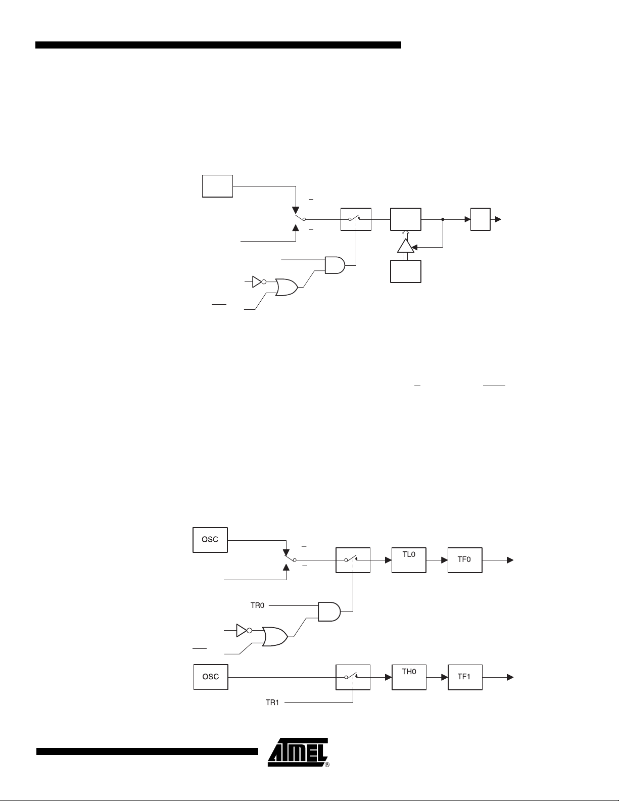
Timer 1 in Mode 3 simply holds its count. The effect is the same as setting TR1 = 0. Timer 0 in
Mode 3 establishes TL0 and TH0 as two separate counters. The logic for Mode 3 on Timer 0 is
shown in Figure 16-4. TL0 uses the Timer 0 control bits: C/T
, GATE, TR0, INT0, and TF0. TH0 is
locked into a timer function (counting machine cycles) and takes over the use of TR1 and TF1
from Timer 1. Thus, TH0 now controls the Timer 1 interrupt.
Mode 3 is for applications requiring an extra 8-bit timer or counter. With Timer 0 in Mode 3, the
AT89LP2052/LP4052 can appear to have three Timer/Counters. When Timer 0 is in Mode 3,
Timer 1 can be turned on and off by switching it out of and into its own Mode 3. In this case,
Timer 1 can still be used by the serial port as a baud rate generator or in any application not
requiring an interrupt.
Figure 16-4. Timer/Counter 0 Mode 3: Two 8-bit Counters
T0 Pin
GATE
C/T = 0
C/T =1
(8 Bits)
Control
Interrupt
3547H–MICRO–5/07
INT0 Pin
Control
(8 Bits)
Interrupt
25

Table 16-1.
TCON = 88H Reset Value = 0000 0000B
Bit Addressable
Bit7 6543210
Symbol Function
TF1 Timer 1 overflow flag. Set by hardware on Timer/Counter overflow. Cleared by hardware when the processor vectors to
TR1 Timer 1 run control bit. Set/cleared by software to turn Timer/Counter on/off.
TF0 Timer 0 overflow flag. Set by hardware on Timer/Counter overflow. Cleared by hardware when the processor vectors to
TR0 Timer 0 run control bit. Set/cleared by software to turn Timer/Counter on/off.
IE1 Interrupt 1 flag. When IT1 is set, IE1 is set by hardware when the external interrupt falling edge is detected, and is cleared
IT1 Interrupt 1 type control bit. Set/cleared by software to specify falling edge/low level triggered external interrupts.
IE0 Interrupt 0 flag. When IT0 is set, IE0 is set by hardware when the external interrupt falling edge is detected, and is cleared
TCON
– Timer/Counter Control Register
TF1 TR1 TF0 TR0 IE1 IT1 IE0 IT0
interrupt routine.
interrupt routine.
by hardware when the CPU vectors to the interrupt routine. When IT1 is cleared, IE1 is sampled and inverted from the
external interrupt pin. The flag will be set or cleared by hardware depending on the state of P3.3.
by hardware when the CPU vectors to the interrupt routine. When IT0 is cleared, IE0 is sampled and inverted from the
external interrupt pin. The flag will be set or cleared by hardware depending on the state of P3.2.
IT0 Interrupt 0 type control bit. Set/cleared by software to specify falling edge/low level triggered external interrupts.
26
AT89LP2052/LP4052
3547H–MICRO–5/07

AT89LP2052/LP4052
.
Table 16-2. TMOD: Timer/Counter Mode Control Register
.
TMOD = 89H Reset Value = 0000 0000B
Not Bit Addressable
GATE C/T M1 M0 GATE C/T M1 M0
76
Timer1 Timer0
Gate Gating control: when set Timer/Counter x is enabled only
while INTx
cleared, Timer x is enabled whenever TRx control bit
is set.
C/T
M1 Mode bit 1
M0 Mode bit 0
Timer or Counter Selector: cleared for Timer operation
(input from internal system clock). Set for Counter
operation (input from Tx input pin).
M1 M0 Mode Operating Mode
000Variable 9 - 16-bit Timer/Counter.
0 1 1 16-bit Auto Reload Timer/Counter.
1028-bit Auto Reload Timer/Counter.
113Split Timer/Counter.
113(Timer 1) Timer/Counter 1 stopped.
pin is high and TRx control pin is set. When
543210
Timer 0 gate bit
Timer 0 counter/timer select bit
Timer 0 M1 bit
Timer 0 M0 bit
8-bit Timer/Counter THz with TLx as 1 - 8-bit prescaler.
8-bit Timer/Counters THx and TLx are cascaded; there is no prescaler.
8-bit auto-reload Timer/Counter THx holds a value which is to be
reloaded into TLx each time it overflows.
(Timer 0) TL0 is an 8-bit Timer/Counter controlled by the standard
Timer 0 control bits. TH0 is an 8-bit timer only controlled by Timer 1
control bits.
3547H–MICRO–5/07
Timer SFR Purpose Address Bit-Addressable
TCON Control 88H Yes
TMOD Mode 89H No
TL0 Timer 0 low-byte 8AH No
TL1 Timer 1 low-byte 8BH No
TH0 Timer 0 high-byte 8CH No
TH1 Timer 1 high-byte 8DH No
TCONB Mode 91H No
RL0 Timer 0 reload low-byte 92H No
RL1 Timer 1 reload low-byte 93H No
RH0 Timer 0 reload high-byte 94H No
RH1 Timer 1 reload high-byte 95H No
27
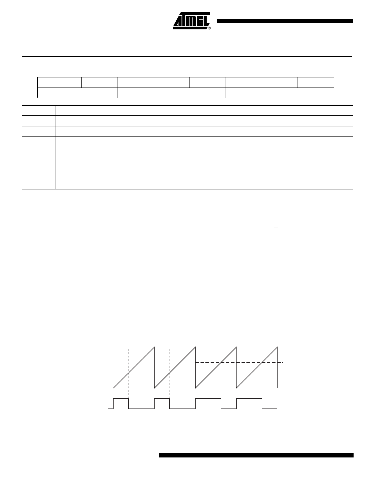
Table 16-3.
TCONB = 91H Reset Value = 0010 0100B
Not Bit Addressable
Bit7 6543210
Symbol Function
PWM1EN Configures Timer 1 for Pulse Width Modulation output on T1 (P3.5).
PWM0EN Configures Timer 0 for Pulse Width Modulation output on T0 (P3.4).
TCONB
PWM1EN PWM0EN PSC12 PSC11 PSC10 PSC02 PSC01 PSC00
– Timer/Counter Control Register B
PSC12
PSC11
PSC10
PSC02
PSC01
PSC00
Prescaler for Timer 1 Mode 0. The number of active bits in TL1 equals PSC1 + 1. After reset PSC1 = 100B which
enables 5 bits of TL1 for compatibility with the 13-bit Mode 0 in AT89S2051.
Prescaler for Timer 0 Mode 0. The number of active bits in TL0 equals PSC0 + 1. After reset PSC0 = 100B which
enables 5 bits of TL0 for compatibility with the 13-bit Mode 0 in AT89C52.
16.5 Pulse Width Modulation
Timer 0 and Timer 1 may be independently configured as 8-bit asymmetrical pulse width modulators (PWM) by setting the PWM0EN or PWM1EN bits in TCONB, respectively. In PWM Mode
the generated waveform is output on the timer's pin, T0 or T1. C/T
PWM mode. In Timer 0's PWM mode, TH0 acts as an 8-bit counter while RH0 stores the 8-bit
compare value. When TH0 is 00H the PWM output is set high. When the TH0 count reaches the
value stored in RH0 the PWM output is set low. Therefore, the pulse width is proportional to the
value in RH0. To prevent glitches writes to RH0 only take effect on the FFH to 00H overflow of
TH0. Timer 1 has the same behavior using TH1 and RH1. See Figure 16-5 for PWM waveform
example. Setting RH0 to 00H will keep the PWM output low.
The PWM will only function if the timer is in Mode 0 or Mode 1. In Mode 0, TL0 acts as a logarithmic prescaler driving TH0 (see Figure 16-6). The PSC0 bits in TCONB control the prescaler
value. In Mode 1, TL0 provides linear prescaling with an 8-bit auto-reload from RL0 (see Figure
16-7).
must be set to “0” when in
28
Figure 16-5. Asymmetrical Pulse Width Modulation
Counter Value (TH0)
Compare Value (RH0)
PWM Output (T0)
AT89LP2052/LP4052
3547H–MICRO–5/07

Figure 16-6. Timer/Counter 1 PWM Mode 0
AT89LP2052/LP4052
RH1
(8 Bits)
OSC
Control
TR1
GATE
INT1 Pin
Figure 16-7. Timer/Counter 1 PWM Mode 1
OSC
Control
TR1
PSC1
RL1
(8 Bits)
TL1
(8 Bits)
TL1
(8 Bits)
OCR1
=
T1
TH1
(8 Bits)
RH1
(8 Bits)
OCR1
=
T1
TH1
(8 Bits)
GATE
INT1 Pin
16.6 Timer/Counter Pin Configuration
In order to use the counter input function or pulse width modulation output feature of Timer 0 or
Timer 1, the Timer pins T0 (P3.4) and T1 (P3.5) must be configured appropriately. See Section
15.7 “Port Alternate Functions” on page 22. For the external counter input function, T0 or T1
should be configured as input-only, or as bidirectional with P3.4 or P3.5 set to “1”. The counter
function may also be triggered by an internal event if T0 or T1 is configured in a bidirectional or
output mode and the port bit is toggled accordingly. To enable a PWM output on T0 or T1, the
pin must be configured in a bidirectional or output mode with P3.4 or P3.5 set to “1”. Setting the
PWM0EN or PWM1En bits in TCONB will not automatically configure the pins as outputs. The
PWM outputs will use a full CMOS push-pull driver if they are in the quasi-bidirectional or output
configurations.
17. External Interrupts
The INT0 and INT1 external interrupt sources can be programmed to be level-activated or transition-activated by setting or clearing bit IT1 or IT0 in Register TCON. If ITx = 0, external
interrupt x is triggered by a detected low at the INTx
tive edge-triggered. In this mode if successive samples of the INTx
pin. If ITx = 1, external interrupt x is nega-
pin show a high in one cycle
3547H–MICRO–5/07
29

and a low in the next cycle, interrupt request flag IEx in TCON is set. Flag bit IEx then requests
the interrupt. Since the external interrupt pins are sampled once each clock cycle, an input high
or low should hold for at least 2 oscillator periods to ensure sampling. If the external interrupt is
transition-activated, the external source has to hold the request pin high for at least two clock
cycles, and then hold it low for at least two clock cycles to ensure that the transition is seen so
that interrupt request flag IEx will be set. IEx will be automatically cleared by the CPU when the
service routine is called if generated in edge-triggered mode. If the external interrupt is level-activated, the external source has to hold the request active until the requested interrupt is actually
generated. Then the external source must deactivate the request before the interrupt service
routine is completed, or else another interrupt will be generated.
18. Serial Interface
The serial port is full-duplex, which means it can transmit and receive simultaneously. It is also
receive-buffered, which means it can begin receiving a second byte before a previously received
byte has been read from the receive register. (However, if the first byte still has not been read
when reception of the second byte is complete, the first byte will be lost.) The serial port receive
and transmit registers are both accessed at Special Function Register SBUF. Writing to SBUF
loads the transmit register, and reading SBUF accesses a physically separate receive register.
The serial port can operate in the following four modes.
Mode 0: Half-Duplex serial data enters or exits through RXD. TXD outputs the shift clock. Eight
data bits are transmitted/received, with the LSB first. The baud rate is fixed at 1/2 the oscillator
frequency.
Mode 1: 10 bits are transmitted (through TXD) or received (through RXD): a start bit (0), 8 data
bits (LSB first), and a stop bit (1). On receive, the stop bit goes into RB8 in Special Function
Register SCON. The baud rate is variable based on Timer 1 overflow.
Mode 2: 11 bits are transmitted (through TXD) or received (through RXD): a start bit (0), 8 data
bits (LSB first), a programmable ninth data bit, and a stop bit (1). On transmit, the 9th data bit
(TB8 in SCON) can be assigned the value of “0” or “1”. For example, the parity bit (P, in the
PSW) can be moved into TB8. On receive, the 9th data bit goes into RB8 in Special Function
Register SCON, while the stop bit is ignored. The baud rate is programmable to either 1/16 or
1/32 the oscillator frequency.
Mode 3: 11 bits are transmitted (through TXD) or received (through RXD): a start bit (0), 8 data
bits (LSB first), a programmable ninth data bit, and a stop bit (1). In fact, Mode 3 is the same as
Mode 2 in all respects except the baud rate, which in Mode 3 is variable based on Timer 1
overflow.
In all four modes, transmission is initiated by any instruction that uses SBUF as a destination
register. Reception is initiated in Mode 0 by the condition RI = 0 and REN = 1. Reception is initiated in the other modes by the incoming start bit if REN = 1.
18.1 Multiprocessor Communications
Modes 2 and 3 have a special provision for multiprocessor communications. In these modes, 9
data bits are received, followed by a stop bit. The ninth bit goes into RB8. Then comes a stop bit.
The port can be programmed such that when the stop bit is received, the serial port interrupt is
activated only if RB8 = 1. This feature is enabled by setting bit SM2 in SCON.
30
The following example shows how to use the serial interrupt for multiprocessor communications.
When the master processor must transmit a block of data to one of several slaves, it first sends
AT89LP2052/LP4052
3547H–MICRO–5/07

AT89LP2052/LP4052
out an address byte that identifies the target slave. An address byte differs from a data byte in
that the 9th bit is “1” in an address byte and “0” in a data byte. With SM2 = 1, no slave is interrupted by a data byte. An address byte, however, interrupts all slaves, so that each slave can
examine the received byte and see if it is being addressed. The addressed slave clears its SM2
bit and prepares to receive the data bytes that follows. The slaves that are not addressed set
their SM2 bits and ignore the data bytes.
The SM2 bit has no effect in Mode 0 but can be used to check the validity of the stop bit in
Mode 1. In a Mode 1 reception, if SM2 = 1, the receive interrupt is not activated unless a valid
stop bit is received.
Table 18-1. SCON – Serial Port Control Register
SCON Address = 98H Reset Value = 0000 0000B
Bit Addressable
SM0/FE SM1 SM2 REN TB8 RB8 T1 RI
Bit7 6543210
(SMOD0 = 0/1)
Symbol Function
Framing error bit. This bit is set by the receiver when an invalid stop bit is detected. The FE bit is not cleared by valid
FE
frames but should be cleared by software. The SMOD0 bit must be set to enable access to the FE bit. FE will be set
regardless of the state of SMOD0.
SM0 Serial Port Mode Bit 0, (SMOD0 must = 0 to access bit SM0)
(1)
Serial Port Mode Bit 1
osc
(2)
/2
/16
osc
SM1
SM0 SM1 Mode Description Baud Rate
0 0 0 shift register f
0 1 1 8-bit UART variable
1 0 2 9-bit UART f
1 1 3 9-bit UART variable
/32 or f
osc
Enables the Automatic Address Recognition feature in Modes 2 or 3. If SM2 = 1 then Rl will not be set unless the received
SM2
9th data bit (RB8) is 1, indicating an address, and the received byte is a Given or Broadcast Address. In Mode 1, if SM2 =
1 then Rl will not be activated unless a valid stop bit was received, and the received byte is a Given or Broadcast Address.
In Mode 0, SM2 should be 0.
REN Enables serial reception. Set by software to enable reception. Clear by software to disable reception.
TB8 The 9th data bit that will be transmitted in Modes 2 and 3. Set or clear by software as desired.
RB8
TI
RI
In Modes 2 and 3, the 9th data bit that was received. In Mode 1, if SM2 = 0, RB8 is the stop bit that was received. In Mode
0, RB8 is not used.
Transmit interrupt flag. Set by hardware at the end of the 8th bit time in Mode 0, or at the beginning of the stop bit in the
other modes, in any serial transmission. Must be cleared by software.
Receive interrupt flag. Set by hardware at the end of the 8th bit time in Mode 0, or halfway through the stop bit time in the
other modes, in any serial reception (except see SM2). Must be cleared by software.
Notes: 1. SMOD0 is located at PCON.6.
= oscillator frequency.
2. f
osc
3547H–MICRO–5/07
31

18.2 Baud Rates
The baud rate in Mode 0 is fixed as shown in the following equation.
The baud rate in Mode 2 depends on the value of the SMOD1 bit in Special Function Register
PCON.7. If SMOD1 = 0 (the value on reset), the baud rate is 1/32 of the oscillator frequency. If
SMOD1 = 1, the baud rate is 1/16 of the oscillator frequency, as shown in the following equation.
Mode 2 Baud Rate
18.2.1 Using Timer 1 to Generate Baud Rates
The Timer 1 overflow rate determines the baud rates in Modes 1 and 3. When Timer 1 is the
baud rate generator, the baud rates are determined by the Timer 1 overflow rate and the value
of SMOD1 according to the following equation.
Modes 1, 3
Baud Rate
The Timer 1 interrupt should be disabled in this application. The Timer itself can be configured
for either timer or counter operation in any of its 3 running modes. In the most typical applications, it is configured for timer operation in auto-reload mode (high nibble of TMOD = 0010B). In
this case, the baud rate is given by the following formula.
Mode 0 Baud Rate
SMOD1
2
--------------------
32
SMOD1
Modes 1, 3
Baud Rate
2
--------------------
SMOD1
2
--------------------
32
32
Oscillator Frequency
------------------------------------------------------ -=
2
(Oscillator Frequency)×=
(Timer 1 Overflow Rate)×=
Oscillator Frequency
------------------------------------------------------ -
×=
256 TH1()–[]
Programmers can achieve very low baud rates with Timer 1 by configuring the Timer to run as a
16-bit auto-reload timer (high nibble of TMOD = 0001B). In this case, the baud rate is given by
the following formula.
SMOD1
Modes 1, 3
Baud Rate
2
--------------------
32
Oscillator Frequency
-------------------------------------------------------- -
×=
65536 RH1,RL1()–[]
32
AT89LP2052/LP4052
3547H–MICRO–5/07

AT89LP2052/LP4052
Table 18-2 lists commonly used baud rates and how they can be obtained from Timer 1.
Table 18-2. Commonly Used Baud Rates Generated by Timer 1
Timer 1
Baud Rate f
Mode 0: 1 MHz 2 X X X X
Mode 2: 375K 12 0 X X X
62.5K 12 102 F4H
19.2K 11.059 1 0 2 DCH
9.6K 11.059 0 0 2 DCH
4.8K 11.059 0 0 2 B8H
2.4K 11.059 0 0 2 70H
1.2K 11.059 0 0 1 FEE0H
137.5 11.986 0 0 1 F55CH
110 6 0 0 1 F958H
110 12 0 0 1 F304H
(MHz) SMOD1
OSC
C/T Mode Reload Value
18.3 More About Mode 0
Serial data enters and exits through RXD. TXD outputs the shift clock. Eight data bits are transmitted/received, with the LSB first. The baud rate is fixed at 1/2 the oscillator frequency. Figure
18-1 shows a simplified functional diagram of the serial port in Mode 0 and associated timing.
Transmission is initiated by any instruction that uses SBUF as a destination register. The “write
to SBUF” signal also loads a “1” into the ninth position of the transmit shift register and tells the
TX Control block to begin a transmission. The internal timing is such that one full machine cycle
will elapse between “write to SBUF” and activation of SEND.
SEND transfers the output of the shift register to the alternate output function line of P3.0, and
also transfers Shift Clock to the alternate output function line of P3.1. At the falling edge of Shift
Clock the contents of the transmit shift register are shifted one position to the right.
As data bits shift out to the right, “0”s come in from the left. When the MSB of the data byte is at
the output position of the shift register, the “1” that was initially loaded into the ninth position is
just to the left of the MSB, and all positions to the left of that contain “0”s. This condition flags the
TX Control block to do one last shift, then deactivate SEND and set TI.
Reception is initiated by the condition REN = 1 and R1 = 0. At the next clock cycle, the RX Control unit writes the bits 11111110 to the receive shift register and activates RECEIVE in the next
clock phase.
RECEIVE enables Shift Clock to the alternate output function line of P3.1. At the falling edge of
Shift Clock the contents of the receive shift register are shifted one position to the left. The value
that comes in from the right is the value that was sampled at the P3.0 pin at rising edge of Shift
Clock.
3547H–MICRO–5/07
As data bits come in from the right, “1”s shift out to the left. When the “0” that was initially loaded
into the right-most position arrives at the left-most position in the shift register, it flags the RX
Control block to do one last shift and load SBUF. Then RECEIVE is cleared and RI is set.
33

Figure 18-1. Serial Port Mode 0
1/2 f
osc
INTERNAL BUS
“1“
WRITE TO SBUF
SEND
SHIFT
RXD (DATA OUT)
TXD (SHIFT CLOCK)
TI
WRITE TO SCON (CLEAR RI)
RI
RECEIVE
SHIFT
RXD (DATA IN)
TXD (SHIFT CLOCK)
34
AT89LP2052/LP4052
INTERNAL BUS
3547H–MICRO–5/07

18.4 More About Mode 1
Ten bits are transmitted (through TXD), or received (through RXD): a start bit (0), 8 data bits
(LSB first), and a stop bit (1). On receive, the stop bit goes into RB8 in SCON. In the
AT89LP2052/LP4052, the baud rate is determined by the Timer 1 overflow rate. The baud rate
is determined by the Timer 1 overflow rate. Figure 18-2 shows a simplified functional diagram of
the serial port in Mode 1 and associated timings for transmit and receive.
Transmission is initiated by any instruction that uses SBUF as a destination register. The “write
to SBUF” signal also loads a “1” into the ninth bit position of the transmit shift register and flags
the TX Control unit that a transmission is requested. Transmission actually commences at S1P1
of the machine cycle following the next rollover in the divide-by-16 counter. Thus, the bit times
are synchronized to the divide-by-16 counter, not to the “write to SBUF” signal.
AT89LP2052/LP4052
The transmission begins when SEND
later, DATA is activated, which enables the output bit of the transmit shift register to TXD. The
first shift pulse occurs one bit time after that.
As data bits shift out to the right, “0”s are clocked in from the left. When the MSB of the data byte
is at the output position of the shift register, the “1” that was initially loaded into the ninth position
is just to the left of the MSB, and all positions to the left of that contain “0”s. This condition flags
the TX Control unit to do one last shift, then deactivate SEND
divide-by-16 rollover after “write to SBUF.”
Reception is initiated by a 1-to-0 transition detected at RXD. For this purpose, RXD is sampled
at a rate of 16 times the established baud rate. When a transition is detected, the divide-by-16
counter is immediately reset, and 1FFH is written into the input shift register. Resetting the
divide-by-16 counter aligns its roll-overs with the boundaries of the incoming bit times.
The 16 states of the counter divide each bit time into 16ths. At the seventh, eighth, and ninth
counter states of each bit time, the bit detector samples the value of RXD. The value accepted is
the value that was seen in at least 2 of the 3 samples. This is done to reject noise. In order to
reject false bits, if the value accepted during the first bit time is not 0, the receive circuits are
reset and the unit continues looking for another 1-to-0 transition. If the start bit is valid, it is
shifted into the input shift register, and reception of the rest of the frame proceeds.
As data bits come in from the right, “1”s shift out to the left. When the start bit arrives at the left
most position in the shift register, (which is a 9-bit register in Mode 1), it flags the RX Control
block to do one last shift, load SBUF and RB8, and set RI. The signal to load SBUF and RB8
and to set RI is generated if, and only if, the following conditions are met at the time the final shift
pulse is generated.
is activated, which puts the start bit at TXD. One bit time
and set TI. This occurs at the tenth
3547H–MICRO–5/07
RI = 0 and
Either SM2 = 0, or the received stop bit = 1
If either of these two conditions is not met, the received frame is irretrievably lost. If both conditions are met, the stop bit goes into RB8, the 8 data bits go into SBUF, and RI is activated. At
this time, whether or not the above conditions are met, the unit continues looking for a 1-to-0
transition in RXD.
35

Figure 18-2. Serial Port Mode 1
TI
TIMER 1
OVERFLOW
WRITE
RXD
TO
SBUF
SAMPLE
TRANSITION
DETECTOR
INTERRUPT
1-TO-0
SMOD1
= 0
÷2
SMOD1
= 1
÷16
SERIAL
PORT
“1”
S
Q
D
CL
START
RX CLOCK
÷16
RX CLOCK
START
BIT
DETECTOR
INTERNAL BUS
SBUF
ZERO DETECTOR
SHIFT
TX CONTROL
TI
RI
RX CONTROL
INPUT SHIFT REG.
LOAD
SBUF
DATA
SEND
LOAD
SBUF
SHIFT
1FFH
(9 BITS)
TXD
SHIFT
TX
CLOCK
WRITE TO SBUF
SEND
DATA
SHIFT
TXD
TI
START BIT
RX
CLOCK
RXD
BIT DETECTOR SAMPLE TIMES
SHIFT
RECEIVE
RI
SBUF
READ
SBUF
INTERNAL BUS
D0 D1 D2 D3 D4 D5 D6 D7
÷16 RESET
START BIT
D0 D1 D2 D3 D4 D5 D6 D7
TRANSMIT
STOP BIT
STOP BIT
36
AT89LP2052/LP4052
3547H–MICRO–5/07

18.5 More About Modes 2 and 3
Eleven bits are transmitted (through TXD), or received (through RXD): a start bit (0), 8 data bits
(LSB first), a programmable ninth data bit, and a stop bit (1). On transmit, the ninth data bit (TB8)
can be assigned the value of “0” or “1”. On receive, the ninth data bit goes into RB8 in SCON.
The baud rate is programmable to either 1/16 or 1/32 of the oscillator frequency in Mode 2.
Mode 3 may have a variable baud rate generated from Timer 1.
Figures 18-3 and 18-4 show a functional diagram of the serial port in Modes 2 and 3. The
receive portion is exactly the same as in Mode 1. The transmit portion differs from Mode 1 only
in the ninth bit of the transmit shift register.
Transmission is initiated by any instruction that uses SBUF as a destination register. The “write
to SBUF” signal also loads TB8 into the ninth bit position of the transmit shift register and flags
the TX Control unit that a transmission is requested. Transmission commences at S1P1 of the
machine cycle following the next rollover in the divide-by-16 counter. Thus, the bit times are synchronized to the divide-by-16 counter, not to the “write to SBUF” signal.
AT89LP2052/LP4052
The transmission begins when SEND
later, DATA is activated, which enables the output bit of the transmit shift register to TXD. The
first shift pulse occurs one bit time after that. The first shift clocks a “1” (the stop bit) into the ninth
bit position of the shift register. Thereafter, only “0”s are clocked in. Thus, as data bits shift out to
the right, “0”s are clocked in from the left. When TB8 is at the output position of the shift register,
then the stop bit is just to the left of TB8, and all positions to the left of that contain “0”s. This condition flags the TX Control unit to do one last shift, then deactivate SEND and set TI. This occurs
at the 11th divide-by-16 rollover after “write to SBUF.”
Reception is initiated by a 1-to-0 transition detected at RXD. For this purpose, RXD is sampled
at a rate of 16 times the established baud rate. When a transition is detected, the divide-by-16
counter is immediately reset, and 1FFH is written to the input shift register.
At the seventh, eighth and ninth counter states of each bit time, the bit detector samples the
value of RXD. The value accepted is the value that was seen in at least 2 of the 3 samples. If the
value accepted during the first bit time is not 0, the receive circuits are reset and the unit continues looking for another 1-to-0 transition. If the start bit proves valid, it is shifted into the input shift
register, and reception of the rest of the frame proceeds.
As data bits come in from the right, “1”s shift out to the left. When the start bit arrives at the left
most position in the shift register (which in Modes 2 and 3 is a 9-bit register), it flags the RX Control block to do one last shift, load SBUF and RB8, and set RI. The signal to load SBUF and RB8
and to set RI is generated if, and only if, the following conditions are met at the time the final shift
pulse is generated:
is activated, which puts the start bit at TXD. One bit time
3547H–MICRO–5/07
RI = 0, and
Either SM2 = 0 or the received 9th data bit = 1
If either of these conditions is not met, the received frame is irretrievably lost, and RI is not set. If
both conditions are met, the received ninth data bit goes into RB8, and the first 8 data bits go
into SBUF. One bit time later, whether the above conditions were met or not, the unit continues
looking for a 1-to-0 transition at the RXD input.
Note that the value of the received stop bit is irrelevant to SBUF, RB8, or RI.
37

Figure 18-3. Serial Port Mode 2
CPU CLOCK
SMOD1
1
SMOD1 0
INTERNAL BUS
38
INTERNAL BUS
AT89LP2052/LP4052
3547H–MICRO–5/07

Figure 18-4. Serial Port Mode 3
TIMER 1
OVERFLOW
WRITE
TO
SBUF
SMOD1
= 0
÷2
SMOD1
= 1
TB8
D
CL
S
Q
ZERO DETECTOR
INTERNAL BUS
SBUF
AT89LP2052/LP4052
TXD
TX
CLOCK
WRITE TO SBUF
SEND
DATA
SHIFT
TXD
TI
START BIT
STOP BIT GEN
RX
CLOCK
STOP BIT
START
÷16
SERIAL
PORT
INTERRUPT
SAMPLE
1-TO-0
TRANSITION
DETECTOR
RXD
D0 D1 D2 D3 D4 D5 D6 D7 TB8
÷16 RESET
RX CLOCK
÷16
START
DETECTOR
TX CONTROL
RX CLOCK
RX CONTROL
BIT
READ
SBUF
TI
RI
LOAD
SBUF
SHIFT
DATA
SEND
LOAD
SBUF
SHIFT
1FFH
INPUT SHIFT REG.
(9 BITS)
SBUF
INTERNAL BUS
SHIFT
STOP BIT
TRANSMIT
BIT DETECTOR SAMPLE TIMES
SHIFT
RECEIVE
RI
3547H–MICRO–5/07
RXD
START BIT
D0 D1 D2 D3 D4 D5 D6 D7 RB8
STOP
BIT
39

18.6 Framing Error Detection
When used for framing error detect, the UART looks for missing stop bits in the communication.
A missing bit will set the FE bit in the SCON register. The FE bit shares the SCON.7 bit with SM0
and the function of SCON.7 is determined by PCON.6 (SMOD0). If SMOD0 is set then SCON.7
functions as FE. SCON.7 functions as SM0 when SMOD0 is cleared. When used as FE,
SCON.7 can only be cleared by software.
18.7 Automatic Address Recognition
Automatic Address Recognition is a feature which allows the UART to recognize certain
addresses in the serial bit stream by using hardware to make the comparisons. This feature
saves a great deal of software overhead by eliminating the need for the software to examine
every serial address which passes by the serial port. This feature is enabled by setting the SM2
bit in SCON. In the 9-bit UART modes, Mode 2 and Mode 3, the Receive Interrupt flag (RI) will
be automatically set when the received byte contains either the “Given” address or the “Broadcast” address. The 9-bit mode requires that the 9th information bit is a “1” to indicate that the
received information is an address and not data.
The 8-bit mode is called Mode 1. In this mode the RI flag will be set if SM2 is enabled and the
information received has a valid stop bit following the 8 address bits and the information is either
a Given or Broadcast address.
Mode 0 is the Shift Register mode and SM2 is ignored.
Using the Automatic Address Recognition feature allows a master to selectively communicate
with one or more slaves by invoking the given slave address or addresses. All of the slaves may
be contacted by using the Broadcast address. Two special Function Registers are used to
define the slave’s address, SADDR, and the address mask, SADEN. SADEN is used to define
which bits in the SADDR are to be used and which bits are “don’t care”. The SADEN mask can
be logically ANDed with the SADDR to create the “Given” address which the master will use for
addressing each of the slaves. Use of the Given address allows multiple slaves to be recognized
while excluding others. The following examples will help to show the versatility of this scheme:
40
Slave 0 SADDR = 1100 0000
SADEN = 1111 1101
Given = 1100 00X0
Slave 1 SADDR = 1100 0000
SADEN = 1111 1110
Given = 1100 000X
In the previous example SADDR is the same and the SADEN data is used to differentiate
between the two slaves. Slave 0 requires a “0” in bit 0 and it ignores bit 1. Slave 1 requires a “0”
in bit 1 and bit 0 is ignored. A unique address for slave 0 would be 1100 0010 since slave 1
requires a “0” in bit 1. A unique address for slave 1 would be 1100 0001 since a “1” in bit 0 will
exclude slave 0. Both slaves can be selected at the same time by an address which has bit 0 = 0
(for slave 0) and bit 1 = 0 (for slave 1). Thus, both could be addressed with 1100 0000.
AT89LP2052/LP4052
3547H–MICRO–5/07

AT89LP2052/LP4052
In a more complex system the following could be used to select slaves 1 and 2 while excluding
slave 0:
Slave 0 SADDR = 1100 0000
SADEN = 1111 1001
Given = 1100 0XX0
Slave 1 SADDR = 1110 0000
SADEN = 1111 1010
Given = 1110 0X0X
Slave 2 SADDR = 1110 0000
SADEN = 1111 1100
Given = 1110 00XX
In the above example the differentiation among the 3 slaves is in the lower 3 address bits. Slave
0 requires that bit 0 = 0 and it can be uniquely addressed by 1110 0110. Slave 1 requires that bit
1 = 0 and it can be uniquely addressed by 1110 and 0101. Slave 2 requires that bit 2 = 0 and its
unique address is 1110 0011. To select Slaves 0 and 1 and exclude Slave 2, use address 1110
0100, since it is necessary to make bit 2 = 1 to exclude slave 2.
The Broadcast Address for each slave is created by taking the logic OR of SADDR and SADEN.
Zeros in this result are treated as don’t cares. In most cases, interpreting the don’t cares as
ones, the broadcast address will be FF hexadecimal.
Upon reset SADDR (SFR address 0A9H) and SADEN (SFR address 0B9H) are loaded with
“0”s. This produces a given address of all “don’t cares” as well as a Broadcast address of all
“don’t cares”. This effectively disables the Automatic Addressing mode and allows the microcontroller to use standard 80C51-type UART drivers which do not make use of this feature.
19. Serial Peripheral Interface
The serial peripheral interface (SPI) allows high-speed synchronous data transfer between the
AT89LP2052/LP4052 and peripheral devices or between multiple AT89LP2052/LP4052
devices. The AT89LP2052/LP4052 SPI features include the following:
• Full-duplex, 3-wire Synchronous Data Transfer
• Master or Slave Operation
• Maximum Bit Frequency = f/4
• LSB First or MSB First Data Transfer
• Four Programmable Bit Rates in Master Mode
• End of Transmission Interrupt Flag
• Write Collision Flag Protection
• Double-buffered Receive
• Double-buffered Transmit (Enhanced Mode Only)
• Wake up from Idle Mode (Slave Mode Only)
3547H–MICRO–5/07
41

The interconnection between master and slave CPUs with SPI is shown in Figure 19-1. The four
pins in the interface are Master-In/Slave-Out (MISO), Master-Out/Slave-In (MOSI), Shift Clock
(SCK), and Slave Select (SS
). The SCK pin is the clock output in master mode, but is the clock
input in slave mode. The MSTR bit in SPCR determines the directions of MISO and MOSI. Also
notice that MOSI connects to MOSI and MISO to MISO. In master mode, SS
may be used as a general-purpose input or output. In slave mode, SS
select an individual device as a slave. When SS
is driven high, the slave’s SPI port is deacti-
/P1.4 is ignored and
must be driven low to
vated and the MOSI/P1.5 pin can be used as a general-purpose input.
Figure 19-1. SPI Master-Slave Interconnection
MSBLSB
Master
8-Bit Shift Register 8-Bit Shift Register
SPI
Clock Generator
Figure 19-2. SPI Block Diagram
Oscillator
Divider
÷4÷8÷32÷64
Select
SPR1
SPI Clock (Mater)
SPR0
MISO
MOSIMOSI
SCK
SS SS
MSB
8-bit Shift Register
Read Data Buffer
Write Data Buffer
MISO
SCK
V
CC
Clock
Logic
MSBLSB
LSB
Clock
Slave
S
M
M
S
Pin Control Logic
S
M
MISO
P1.6
MOSI
P1.5
SCK
1.7
SS
P1.4
42
SPI Control
WCOL
SPIF
SPI Status Register
AT89LP2052/LP4052
SPI Interrupt
Request
MSTR
SPE
8
Internal
Data Bus
SPE
DORD
MSTR
8
SPIE
SPE
SPI Control Register
8
DORD
MSTR
CPOL
CPHA
SPR1
SPR0
3547H–MICRO–5/07

19.1 Normal Mode
The SPI has two modes of operation: normal (non-buffered write) and enhanced (buffered
write). In normal mode, writing to the SPI data register (SPDR) of the master CPU starts the SPI
clock generator and the data written shifts out of the MOSI pin and into the MOSI pin of the slave
CPU. Transmission may start after an initial delay while the clock generator waits for the next full
bit slot of the specified baud rate. After shifting one byte, the SPI clock generator stops, setting
the end of transmission flag (SPIF) and transferring the received byte to the read buffer (SPDR).
If both the SPI interrupt enable bit (SPIE) and the serial port interrupt enable bit (ES) are set, an
interrupt is requested. Note that SPDR refers to either the write data buffer or the read data
buffer, depending on whether the access is a write or read. In normal mode, because the write
buffer is transparent (and a write access to SPDR will be directed to the shift buffer), any attempt
to write to SPDR while a transmission is in progress will result in a write collision with WCOL set.
However, the transmission will still complete normally, but the new byte will be ignored and a
new write access to SPDR will be necessary.
19.2 Enhanced Mode
Enhanced mode is similar to normal mode except that the write buffer holds the next byte to be
transmitted. Writing to SPDR loads the write buffer and sets WCOL to signify that the buffer is
full and any further writes will overwrite the buffer. WCOL is cleared by hardware when the buffered byte is loaded into the shift register and transmission begins. If the master SPI is currently
idle, i.e. if this is the first byte, then after loading SPDR, transmission of the byte starts and
WCOL is cleared immediately. While this byte is transmitting, the next byte may be written to
SPDR. The Load Enable flag (LDEN) in SPSR can be used to determine when transmission has
started. LDEN is asserted during the first four bit slots of a SPI transfer. The master CPU should
first check that LDEN is set and that WCOL is cleared before loading the next byte. In enhanced
mode, if WCOL is set when a transfer completes, i.e. the next byte is available, then the SPI
immediately loads the buffered byte into the shift register, resets WCOL, and continues transmission without stopping and restarting the clock generator. As long as the CPU can keep the
write buffer full in this manner, multiple bytes may be transferred with minimal latency between
bytes.
AT89LP2052/LP4052
3547H–MICRO–5/07
43

Table 19-1. SPCR – SPI Control Register
SPCR Address = D5H Reset Value = 0000 0000B
Not Bit Addressable
SPIE SPE DORD MSTR CPOL CPHA SPR1 SPR0
Bit76543210
Symbol Function
SPIE SPI interrupt enable. This bit, in conjunction with the ES bit in the IE register, enables SPI interrupts: SPIE = 1 and ES = 1
enable SPI interrupts. SPIE = 0 disables SPI interrupts.
SPE SPI enable. SPE = 1 enables the SPI channel and connects SS, MOSI, MISO and SCK to pins P1.4, P1.5, P1.6, and
P1.7. SPE = 0 disables the SPI channel.
DORD Data order. DORD = 1 selects LSB first data transmission. DORD = 0 selects MSB first data transmission.
MSTR Master/slave select. MSTR = 1 selects Master SPI mode. MSTR = 0 selects slave SPI mode.
CPOL Clock polarity. When CPOL = 1, SCK is high when idle. When CPOL = 0, SCK of the master device is low when not
transmitting. Please refer to figure on SPI clock phase and polarity control.
CPHA Clock phase. The CPHA bit together with the CPOL bit controls the clock and data relationship between master and
slave. Please refer to figure on SPI clock phase and polarity control.
SPR0
SPR1
Notes: 1. Set up the clock mode before enabling the SPI: set all bits needed in SPCR except the SPE bit, then set SPE.
SPI clock rate select. These two bits control the SCK rate of the device configured as master. SPR1 and SPR0 have no
effect on the slave. The relationship between SCK and the oscillator frequency, F
SPR1 SPR0 SCK
00 f/4
01 f/8
10 f/32
11 f/64
2. Enable the master SPI prior to the slave device.
3. Slave echoes master on the next Tx if not loaded with new data.
, is as follows:
OSC.
44
AT89LP2052/LP4052
3547H–MICRO–5/07

AT89LP2052/LP4052
Table 19-2. SPSR – SPI Status Register
SPSR Address = AAH Reset Value = 000X X000B
Not Bit Addressable
SPIF WCOL
Bit76543210
Symbol Function
SPIF SP interrupt flag. When a serial transfer is complete, the SPIF bit is set and an interrupt is generated if SPIE = 1 and
ES = 1. The SPIF bit is cleared by reading the SPI status register followed by reading/writing the SPI data register.
WCOL When ENH = 0: Write collision flag. The WCOL bit is set if the SPI data register is written during a data transfer. During
data transfer, the result of reading the SPDR register may be incorrect, and writing to it has no effect. The WCOL bit
(and the SPIF bit) are cleared by reading the SPI status register followed by reading/writing the SPI data register.
When ENH = 1: WCOL works in Enhanced mode as Tx Buffer Full. Writing during WCOL = 1 in enhanced mode will
overwrite the waiting data already present in the Tx Buffer. In this mode, WCOL is no longer reset by the SPIF reset but
is reset when the write buffer has been unloaded into the serial shift register.
LDEN Load enable for the Tx buffer in enhanced SPI mode.
When ENH is set, it is safe to load the Tx Buffer while LDEN = 1 and WCOL = 0. LDEN is high during bits 0 - 3 and is low
during bits 4 - 7 of the SPI serial byte transmission time frame.
DISSO Disable slave output bit.
When set, this bit causes the MISO pin to be tri-stated so more than one slave device can share the same interface with
a single master. Normally, the first byte in a transmission could be the slave address and only the selected slave should
clear its DISSO bit.
ENH Enhanced SPI mode select bit. When ENH = 0, SPI is in normal mode, i.e. without write double buffering.
When ENH = 1, SPI is in enhanced mode with write double buffering. The Tx buffer shares the same address with the
SPDR register.
LDEN – – – DISSO ENH
Table 19-3. SPDR – SPI Data Register
SPDR Address = 86H Reset Value = 00H (after cold reset)
Not Bit Addressable
SPD7 SPD6 SPD5 SPD4 SPD3 SPD2 SPD1 SPD0
Bit76543210
3547H–MICRO–5/07
unchanged (after warm reset)
45

Figure 19-3. SPI Shift Register Diagram
7
Serial In
Transmit
Byte
19.3 Serial Clock Generator
The CPHA (Clock PHAse), CPOL (Clock POLarity), and SPR (Serial Peripheral clock Rate =
baud rate) bits in SPCR control the shape and rate of SCK. The two SPR bits provide four possible clock rates when the SPI is in master mode. In slave mode, the SPI will operate at the rate of
the incoming SCK as long as it does not exceed the maximum bit rate. There are also four possible combinations of SCK phase and polarity with respect to the serial data. CPHA and CPOL
determine which format is used for transmission. The SPI data transfer formats are shown in
Figures 19-4 and and 19-5. To prevent glitches on SCK from disrupting the interface, CPHA,
CPOL, and SPR should be set up before the interface is enabled, and the master device should
be enabled before the slave device(s).
8
2:1
MUX
Serial Master Serial Slave
DQ
LATCH
CLK
8
Parallel Master
(Write Buffer)
8 8
DQ
LATCH
CLK
2:1
MUX
DQ
LATCH
CLK
Parallel Slave
(Read Buffer)
DQ
LATCH
CLK
Serial Out
Receive
Byte
8
46
AT89LP2052/LP4052
3547H–MICRO–5/07

Figure 19-4. SPI Transfer Format with CPHA = 0
Note: *Not defined but normally MSB of character just received
Figure 19-5. SPI Transfer Format with CPHA = 1
SCK CYCLE #
(FOR REFERENCE)
SCK (CPOL = 0)
SCK (CPOL = 1)
1 2 3 4 5 6 7 8
AT89LP2052/LP4052
MOSI
(FROM MASTER)
MISO
(FROM SLAVE)
SS (TO SLAVE)
Note: *Not defined but normally LSB of previously transmitted character
MSB 6 5 4 3 2
MSB
*
65432
19.4 SPI Pin Configuration
Before using the Serial Peripheral Interface the four SPI pins – SCK, MISO, MOSI and SS –
must be properly configured for the desired functionality. See Section 15.7 “Port Alternate Func-
tions” on page 22. When the SPI is in Master mode, SCK and MOSI must be configured as
bidirectional or output, with P1.7 and P1.5 set to “1”. MISO should be input-only, or bidirectional
with P1.6 set to “1”. When the SPI is in Slave mode, SCK, MOSI and SS must be configured as
input-only, or as bidirectional with P1.7, P1.6 and P1.4 set to “1”. MISO should be set as bidirectional or output, with P1.6 set to “1”. If all four pins are set as bidirectional and their respectively
port bits are all “1”, it is possible to switch between Master and Slave mode without reconfiguring
the pins.
1 LSB
1 LSB
3547H–MICRO–5/07
47

20. Analog Comparator
A single analog comparator is provided on the AT89LP2052/LP4052. Comparator operation is
such that the output is a logic “1” when the positive input AIN0 (P1.0) is greater than the negative
input AIN1 (P1.1). Otherwise, the output is a zero. Setting the CEN bit in ACSR enables the
comparator. When the comparator is first enabled, the comparator output and interrupt flag are
guaranteed to be stable only after 10 µs. The corresponding comparator interrupt should not be
enabled during that time, and the comparator interrupt flag must be cleared before the interrupt
is enabled in order to prevent an immediate interrupt service. Before enabling the comparator
the analog inputs should be tri-stated by putting P1.0 and P1.1 into input-only mode. See Sec-
tion 15.5 “Port 1 Analog Functions” on page 21.
The comparator output is internally tied to the P3.6 pin. Instructions which read the pins of P3
will also read the comparator output directly. Read-Modify-Write instructions or Write instructions
to P3.6 will access bit 6 of the Port 3 register without affecting the comparator.
The comparator may be configured to cause an interrupt under a variety of output value conditions by setting the CM bits in ACSR. The comparator interrupt flag CF in ACSR is set whenever
the comparator output matches the condition specified by CM. The flag may be polled by software or may be used to generate an interrupt and must be cleared by software. The EC bit in IE
must be set before CF will generate an interrupt.
20.1 Comparator Interrupt with Debouncing
The comparator output is sampled every clock cycle. The conditions on the analog inputs may
be such that the comparator output will toggle excessively. This is especially true if applying slow
moving analog inputs. Three debouncing modes are provided to filter out this noise. In debouncing mode, the comparator uses Timer 1 to modulate its sampling time. When a relevant
transition occurs, the comparator waits until two Timer 1 overflows have occurred before resampling the output. If the new sample agrees with the expected value, CF is set. Otherwise the
event is ignored. The filter may be tuned by adjusting the time-out period of Timer 1. Because
Timer 1 is free running, the debouncer must wait for two overflows to guarantee that the sampling delay is at least 1 time-out period. Therefore after the initial edge event, the interrupt may
occur between 1 and 2 time-out periods later. See Figure 20-1.
48
By default the comparator is disabled during Idle mode. To allow the comparator to function during Idle, the CIDL bit in ACSR must be set. When CIDL is set, the comparator can be used to
wake-up the CPU from Idle if the comparator interrupt is enabled. The comparator is always disabled during Power-down mode.
Figure 20-1. Negative Edge with Debouncing Example
Comparator Out
Timer 1 Overflow
CF
Start Compare
Start Compare
AT89LP2052/LP4052
3547H–MICRO–5/07

AT89LP2052/LP4052
Table 20-1.
ACSR = 97H Reset Value = XXX0 0000B
Not Bit Addressable
Bit76543210
Symbol Function
CIDL Comparator Idle Enable. If CIDL = 1 the comparator will continue to operate during Idle mode. If CIDL = 0 the
CF Comparator Interrupt Flag. Set when the comparator output meets the conditions specified by the CM [2:0] bits and CEN
CEN Comparator Enable. Set this bit to enable the comparator. Clearing this bit will force the comparator output low and
CM [2:0] Comparator Interrupt Mode
ACSR
– Analog Comparator Control & Status Register
––
comparator is powered down during Idle mode. The comparator is always shut down during Power-down mode.
is set. The flag must be cleared by software. The interrupt may be enabled/disabled by setting/clearing bit 6 of IE.
prevent further events from setting CF.
1 0 Interrupt Mode
2
000Negative (Low) level
001Positive edge
010Toggle with debounce
011Positive edge with debounce
100Negative edge
101Toggle
110Negative edge with debounce
111Positive (High) level
CIDL CF CEN CM2 CM1 CM0
3547H–MICRO–5/07
49

21. Programmable Watchdog Timer
The programmable Watchdog Timer (WDT) protects the system from incorrect execution by triggering a system reset when it times out after the software has failed to feed the timer prior to the
timer overflow. The WDT counts CPU clock cycles. The prescaler bits, PS0, PS1 and PS2 in
SFR WDTCON are used to set the period of the Watchdog Timer from 16K to 2048K clock
cycles. The WDT is disabled by Reset and during Power-down mode. When the WDT times out
without being serviced, an internal RST pulse is generated to reset the CPU. See Table 21-1 for
the available WDT period selections.
Table 21-1. Watchdog Timer Time-out Period Selection
WDT Prescaler Bits
000 16K
001 32K
010 64K
011 128K
100 256K
101 512K
1 1 0 1024K
1 1 1 2048K
Note: *The WDT time-out period is dependent on the system clock frequency.
Period*
(Clock Cycles)PS2 PS1 PS0
The Watchdog Timer consists of a 14-bit timer with 7-bit programmable prescaler. Writing the
sequence 1EH/E1H to the WDTRST register enables the timer. When the WDT is enabled, the
WDTEN bit in WDTCON will be set to “1”. To prevent the WDT from generating a reset when if
overflows, the watchdog feed sequence must be written to WDTRST before the end of the timeout period. To feed the watchdog, two write instructions must be sequentially executed successfully. Between the two write instructions, SFR reads are allowed, but writes are not allowed. The
instructions should move 1EH to the WDTRST register and then 1EH to the WDTRST register.
An incorrect feed or enable sequence will cause an immediate watchdog reset. The program
sequence to feed or enable the watchdog timer is as follows:
50
MOV WDTRST, #01Eh
MOV WDTRST, #0E1h
AT89LP2052/LP4052
3547H–MICRO–5/07

AT89LP2052/LP4052
Table 21-2. WDTCON – Watchdog Control Register
S
WDTCON Address = A7H Reset Value = 0000 XX00B
Not Bit Addressable
PS2 PS1 PS0 WDIDLE
Bit76543210
Symbol Function
PS2
PS1
PS0
WDIDLE Disable/enable the Watchdog Timer in IDLE mode. When WDIDLE = 0, WDT continues to count in IDLE mode. When
WDTOVF Watchdog Overflow Flag. Set when a WDT reset is generated by the WDT timer overflow. Also set when an incorrect
WDTEN Watchdog Enable Flag. This bit is READ-ONLY and reflects the status of the WDT (whether it is running or not). The
Prescaler bits for the watchdog timer (WDT). When all three bits are cleared to 0, the watchdog timer has a nominal
period of 16K clock cycles. When all three bits are set to 1, the nominal period is 2048K clock cycles.
WDIDLE = 1, WDT freezes while the device is in IDLE mode.
sequence is written to WDTRST. Must be cleared by software.
WDT is disabled after any reset and must be re-enabled by writing 1EH/E1H to WDTRST
–
– WDTOVF WDTEN
Table 21-3. WDTRST – Watchdog Reset Register
WDTCON Address = A6H (Write-Only)
Not Bit Addressable
––––––––
Bit76543210
The WDT is enabled by writing the sequence 1EH/E1H to the WDTRST SFR. The current status may be checked by reading
the WDTEN bit in WDTCON. To prevent the WDT from resetting the device, the same sequence 1EH/E1H must be written to
WDTRST before the time-out interval expires.
22. Instruction Set Summary
The AT89LP2052/LP4052 is fully binary compatible with the MCS-51 instruction set. The
difference between the AT89LP2052/LP4052 and the standard 8051 is the number of cycles
required to execute an instruction. Instructions in the AT89LP2052/LP4052 may take 1, 2, 3 or 4
clock cycles to complete. The execution times of most instructions may be computed using
Table 22-1.
3547H–MICRO–5/07
51

Table 22-1. Generic Instruction Execution Times and Exceptions
Instruction Type Cycle Count
Most arithmetic, logical, bit and transfer instructions # bytes
Branches and Calls # bytes + 1
Single Byte Indirect (i.e. ADD A, @Ri, etc.) 2
RET, RETI 4
MOVC 3
MUL 2
DIV 4
INC DPTR 2
Table 22-2. Detailed Arithmetic Instruction Summary
Clock Cycles
Arithmetic Instruction Bytes
ADD A, Rn 1 12 1 28-2F
ADD A, direct 2 12 2 25
ADD A, @Ri 1 12 2 26-27
ADD A, #data 2 12 2 24
ADDC A, Rn 1 12 1 38-3F
8051 LP2052
Hex Code
ADDC A, direct 2 12 2 35
ADDC A, @Ri 1 12 2 36-37
ADDC A, #data 2 12 2 34
SUBB A, Rn 1 12 1 98-9F
SUBB A, direct 2 12 2 95
SUBB A, @Ri 1 12 2 96-97
SUBB A, #data 2 12 2 94
INC Rn 1 12 1 08-0F
INC direct 2 12 2 05
INC @Ri 1 12 2 06-07
INC A 1 12 1 04
DEC Rn 1 12 1 18-1F
DEC direct 2 12 2 15
DEC @Ri 1 12 2 16-17
DEC A 1 12 1 14
INC DPTR 1 24 2 A3
MUL AB 1 48 2 A4
DIV AB 1 48 4 84
DA A 1 12 1 D4
52
AT89LP2052/LP4052
3547H–MICRO–5/07

AT89LP2052/LP4052
Table 22-3. Detailed Logical Instruction Summary
Clock Cycles
Logical Instruction Bytes
CLR A 1 12 1 E4
CPL A 1 12 1 F4
ANL A, Rn 1 12 1 58-5F
ANL A, direct 2 12 2 55
ANL A, @Ri 1 12 2 56-57
ANL A, #data 2 12 2 54
ANL direct, A 2 12 2 52
ANL direct, #data 3 24 3 53
ORL A, Rn 1 12 1 48-4F
ORL A, direct 2 12 2 45
ORL A, @Ri 1 12 2 46-47
ORL A, #data 2 12 2 44
ORL direct, A 2 12 2 42
ORL direct, #data 3 24 3 43
8051 LP2052
Hex Code
XRL A, Rn 1 12 1 68-6F
XRL A, direct 2 12 2 65
XRL A, @Ri 1 12 2 66-67
XRL A, #data 2 12 2 64
XRL direct, A 2 12 2 62
XRL direct, #data 3 24 3 63
RL A 1 12 1 23
RLC A 1 12 1 33
RR A 1 12 1 03
RRC A 1 12 1 13
SWAP A 1 12 1 C4
3547H–MICRO–5/07
53

Table 22-4. Detailed Data Transfer Instruction Summary
Clock Cycles
Data Transfer Instruction Bytes
MOV A, Rn 1 12 1 E8-EF
MOV A, direct 2 12 2 E5
MOV A, @Ri 1 12 2 E6-E7
MOV A, #data 2 12 2 74
MOV Rn, A 1 12 1 F8-FF
MOV Rn, direct 2 24 2 A8-AF
MOV Rn, #data 2 12 2 78-7F
MOV direct, A 2 12 2 F5
MOV direct, Rn 2 24 2 88-8F
MOV direct, direct 3 24 3 85
MOV direct, @Ri 2 24 2 86-87
MOV direct, #data 3 24 3 75
MOV @Ri, A 1 12 1 F6-F7
MOV @Ri, direct 2 24 2 A6-A7
MOV @Ri, #data 2 12 2 76-77
MOV DPTR, #data16 3 24 3 90
8051 LP2052
Hex Code
MOVC A, @A+DPTR 1 24 3 93
MOVC A, @A+PC 1 24 3 83
PUSH direct 2 24 2 C0
POP direct 2 24 2 D0
XCH A, Rn 1 12 1 C8-CF
XCH A, direct 2 12 2 C5
XCH A, @Ri 1 12 2 C6-C7
XCHD A, @Ri 1 12 2 D6-D7
54
AT89LP2052/LP4052
3547H–MICRO–5/07

AT89LP2052/LP4052
Table 22-5. Detailed Bit Instruction Summary
Clock Cycles
Bit Instruction Bytes
CLR C 1 12 1 C3
CLR bit 2 12 2 C2
SETB C 1 12 1 D3
SETB bit 2 12 2 D2
CPL C 1 12 1 B3
CPL bit 2 12 2 B2
ANL C, bit 2 24 2 82
ANL C, /bit 2 24 2 B0
ORL C, bit 2 24 2 72
ORL C, /bit 2242A0
MOV C, bit 2 12 2 A2
MOV bit, C 2 24 2 92
Table 22-6. Detailed Branching Instruction Summary
Clock Cycles
Branching Instruction Bytes
JC rel 2 24 3 40
JNC rel 2 24 3 50
JB bit, rel 3 24 4 20
JNB bit, rel 3 24 4 30
JBC bit, rel 3 24 4 10
JZ rel 2 24 3 60
JNZ rel 2 24 3 70
SJMP rel 224380
ACALL addr11 2 24 3 11,31,51,7
LCALL addr16 3 24 4 12
RET 124422
RETI 124432
AJMP addr11 2 24 3 01,21,41,6
LJMP addr16 3 24 4 02
JMP @A+DPTR 1 24 2 73
CJNE A, direct, rel 3 24 4 B5
CJNE A, #data, rel 3 24 4 B4
CJNE Rn, #data, rel 3 24 4 B8-BF
CJNE @Ri, #data, rel 3 24 4 B6-B7
DJNZ Rn, rel 2 24 3 D8-DF
DJNZ direct, rel 3 24 4 D5
NOP 112100
Hex Code8051 LP2052
Hex Code8051 LP2052
1,91,B1,D1
,F1
1,81,A1,C1
,E1
3547H–MICRO–5/07
55

23. Programming the Flash Memory
The AT89LP2052/LP4052 offers 2/4K bytes of In-System Programmable (ISP) non-volatile
Flash code memory. In addition, the device contains a 32-byte User Signature Row and a
32-byte read-only Atmel Signature Row. The memory organization is shown in Table 23-1. The
Memory is divided into pages of 32 bytes each. A single read or write command may only
access a single page in the memory.
Table 23-1. Memory Organization
Device # Code Size Page Size # Pages Address Range
AT89LP2052 2K bytes 32 bytes 64 0000H - 07FFH
AT89LP4052 4K bytes 32 bytes 128 0000H - 0FFFH
The AT89LP2052/LP4052 provides two flexible interfaces for programming the Flash memory: a
parallel interface which uses 10 pins; and a serial interface which uses the 4 SPI pins. The parallel and serial programming algorithms are identical. Both interfaces support the same
command format where each command is issued to the device one byte at a time. Commands
consist of a preamble byte for noise immunity, an opcode byte, two address bytes, and from 1 to
32 data bytes. Figure 23-1 shows a simplified flow chart of a command sequence.
Figure 23-1. Command Sequence Flow Chart
Input Preamble
(AAh)
Input Opcode
Input Address
High Byte
Input Address
Low Byte
Input/Output
Data
Address +1
56
AT89LP2052/LP4052
3547H–MICRO–5/07

AT89LP2052/LP4052
23.1 Programming Command Summary
Command Preamble Opcode Addr High Addr Low Data 0 Data n
Program Enable
(1)
Chip Erase 1010 1010 1000 1010
Read Status 1010 1010 0110 0000 xxxx xxxx xxxx xxxx Status Out
Load Code Page Buffer
Write Code Page
Read Code Page
Write User Fuses
Read User Fuses
Write Lock Bits
Read Lock Bits
(4)
(4)
Write User Signature Page
Read User Signature Page
Read Atmel Signature Page
(2)
(2)
(2)
(3)
(3)
(2)
(2)
(2)(5)
Notes: 1. Program Enable must be the first command issued after entering into programming mode.
2. Any number of Data bytes from 1 to 32 may be written/read. The internal address is incremented between each byte.
3. Fuse Bit Definitions:
1010 1010 1010 1100 0101 0011
1010 1010 0101 0001 xxxx xxxx xxx DataIn 0 ... DataIn n
1010 1010 0101 0000 xxxx DataIn 0 ... DataIn n
1010 1010 0011 0000 xxxx DataOut 0 ... DataOut n
A11
A10A9A8
A11
A10A9A8
A7
A7
A6
A6
A5
A5
1010 1010 1110 0001 xxxx xxxx xxxx xxxx xxxx
1010 1010 0110 0001 xxxx xxxx xxxx xxxx xxxx
1010 1010 1110 0100 xxxx xxxx xxxx xxxx xxxx xx
1010 1010 0110 0100 xxxx xxxx xxxx xxxx xxxx xx
1010 1010 0101 0010 xxxx xxxx xxx DataIn 0 ... DataIn n
1010 1010 0011 0010 xxxx xxxx xxx DataOut 0 ... DataOut n
1010 1010 0011 1000 xxxx xxxx xxx DataOut 0 ... DataOut n
B4
B4
B4
B4
B4
B4
B3
B3
B3
B3
B3
B3
B2
B2
B2
B2
B2
B2
B1
B1
B1
B1
B1
B1
B0
B0
B0
B0
B0
B0
F3F2F1
F3F2F1
L1
L1
F0
F0
L0
L0
Bit 0
ISP Enable*
Bit 1
XTAL Osc Bypass
Bit 2
User Row Programming
Bit 3
System Clock Out
Enable = 0/Disable = 1
Enable = 0/Disable = 1
Enable = 0/Disable = 1
Enable = 0/Disable = 1
*The AT89LP2052/LP4052 has ISP enabled by default from the factory. However, if ISP is later disabled, the ISP Enable
Fuse must be enabled by using Parallel Programming before entering ISP mode.
When disabling the ISP fuse during ISP, the current ISP session will remain active until RST is brought low.
4. Lock Bit Definitions:
Bit 0
Bit 1
Lock Bit 1
Lock Bit 2
Locked = 0/Unlocked = 1
Locked = 0/Unlocked = 1
5. Atmel Signature Byte:
AT89LP2052: Address 00H = 1EH
01H = 25H
02H = FFH
AT89LP4052: Address 00H = 1EH
01H = 45H
02H = FFH
6. Symbol Key:
A: Page Address Bit
B: Byte Address Bit
F: Fuse Bit Data
L: Lock Bit Data
x: Don’t Care
3547H–MICRO–5/07
57

23.2 Status Register
The current state of the memory may be accessed by reading the status register. The status register is shown in Table 23-2.
Table 23-2.
Bit76543210
Symbol Function
LOAD
SUCCESS
WRTINH
BUSY
Status
Register
––––
Load flag. Cleared low by the load page buffer command and set high by the next memory write. This flag signals that
the page buffer was previously loaded with data by the load page buffer command.
Success flag. Cleared low at the start of a programming cycle and will only be set high if the programming cycle
completes without interruption from the brownout detector.
Write Inhibit flag. Cleared low by the brownout detector (BOD) whenever programming is inhibited due to VCC falling
below the minimum required programming voltage. If a BOD episode occurs during programming, the SUCCESS flag
will remain low after the cycle is complete. WRTINH
Busy flag. Cleared low whenever the memory is busy programming or if write is currently inhibited.
low also forces BUSY low.
LOAD SUCCESS WRTINH BUSY
23.3 DATA Polling
The AT89LP2052/LP4052 implements DATA polling to indicate the end of a programming cycle.
While the device is busy, any attempted read of the last byte written will return the data byte with
the MSB complemented. Once the programming cycle has completed, the true value will be
accessible. During Erase the data is assumed to be FFH and DATA
When writing multiple bytes in a page, the DATA
value will be the last data byte loaded before
programming begins, not the written byte with the highest physical address within the page.
polling will return 7FH.
23.4 Parallel Programming
Parallel Programming Mode is enabled by applying VPP to the RST pin. The connections
required during parallel mode are shown in Figure 23-2. During parallel programming, Port 1 is
configured as an 8-bit wide bidirectional command bus. Data on P1 is strobed by a positive
pulse on the XTAL1 pin. No other clock is required. The interface is enabled by pulling CS
low. P3.1 acts as RDY/BSY
of the state of CS
58
AT89LP2052/LP4052
(P3.2)
, and will be pulled low to indicate that the device is busy regardless
.
3547H–MICRO–5/07

AT89LP2052/LP4052
Figure 23-2. Flash Parallel Programming Device Connections
R DY/BSY
AT89LP2052/LP4052
P3.1
2.7 to 5.5V
VCC
CS
P3.2
X TAL 1
P1
RST
DATA
V
PP
GND
Note: Sampling of pin P3.1 (RDY/BSY) is optional. During Parallel Programming, P3.1 will be pulled low
while the device is busy. Note that it does not require an external passive pull-up to V
CC
.
While CS is high, the interface is reset to its default state and P1 is tri-stated. CS should be
brought low before the first byte of a command is issued, and should return high only after the
last byte of the command has been strobed. Figure 23-3 shows a generic parallel write command sequence. Command, address, and data bytes are sampled from P1 on the rising edge of
the XTAL1 pulse. Figure 23-4 shows a generic parallel read command sequence. Command
and address bytes are sampled from P1 on the rising edge of the XTAL1 pulse. At the falling
edge of the fourth XTAL1 pulse the device enables P1 to output data. The data remains on P1
until CS
is brought high. During reads the parallel programmer should tri-state P1 before the
negative edge of the fourth XTAL1 pulse to avoid bus contention.
Figure 23-3. Parallel Write Command Sequence
CS
XTAL1
P1
AAh OPCODE ADDRH ADDRL DATAIN
Figure 23-4. Parallel Read Command Sequence
CS
XTAL1
P1
3547H–MICRO–5/07
AAh OPCODE ADDRH ADDRL DATAOUT
59

23.4.1 Power-up Sequence
Execute the following sequence to power-up the device before parallel programming.
1. Apply power between VCC and GND pins.
2. After V
3. Wait 2 ms for the internal Power-on Reset to time out.
4. Bring P3.2 to “H” and then wait 10 µs.
5. Raise RST/V
6. After V
Figure 23-5. Parallel Mode Power-up Operation
has settled, wait 10 µs and bring RST to “H”.
CC
to 12V to enable the parallel programming modes.
PP
has settled, wait an additional 10 µs before programming.
PP
V
CC
RST
P3.2
XTAL1
HIGH ZP1
V
PP
V
IH
23.4.2 Power-down Sequence
Execute the following sequence to power-down the device after parallel programming.
1. Tri-state P1.
2. Bring RST/V
3. Bring XTAL and P3.2 to “L”.
4. Bring RST to “L” and wait 10 µs.
5. Power off V
Figure 23-6. Parallel Mode Power-down Operation
Note: The waveforms on this page are not to scale.
V
CC
RST
P3.2
XTAL1
down from 12V to VCC and wait 10 µs.
PP
.
CC
HIGH ZP1
V
PP
V
IH
60
AT89LP2052/LP4052
3547H–MICRO–5/07

23.4.3 Program Enable
AT89LP2052/LP4052
Function:
• Enables the programming interface to receive commands.
• Program Enable must be the first command issued in any programming session. In parallel
programming a session is active while RST remains at V
is active while RST remains at V
CC
.
Usage:
. In serial programming a session
PP
23.4.4 Chip Erase
1. Bring CS
(P3.2) low.
2. Drive P1 to AAh and pulse XTAL1 high.
3. Drive P1 to ACh and pulse XTAL1 high.
4. Drive P1 to 53h and pulse XTAL1 high.
5. Bring CS
high.
Figure 23-7. Program Enable Sequence
CS
XTAL1
P1
AAh ACh 53h
Function:
• Erases (programs FFh to) the entire 2/4-Kbyte memory array.
• Erases User Signature Row if User Row Programming Fuse bit is enabled.
• Lockbit1 and Lockbit2 are programmed to “unlock” state.
Usage:
1. Bring CS
(P3.2) low.
2. Drive P1 to AAh and pulse XTAL1 high.
3. Drive P1 to 8Ah and pulse XTAL1 high.
4. Bring CS
high.
5. Wait 4 ms, monitor P3.1, or poll data/status.
3547H–MICRO–5/07
Figure 23-8. Chip Erase Sequence
CS
XTAL1
P1
RDY/BSY
Note: The waveforms on this page are not to scale.
AAh 8Ah
61

23.4.5 Load Code Page Buffer
Function:
• Loads 1 page (1 to 32 bytes) of data into the temporary page buffer but does not start
programming.
• Use for interruptible loads or loading non-contiguous bytes to a page.
• The byte address (offset in page) is initialized to bits [4:0] of the low address byte. One byte
of data is loaded from P1 for the current address by the positive edge of a XTAL1 pulse. The
internal address is incremented by one on the negative edge of the XTAL1 pulse. The
address will wrap around to the 1st byte of the page when incremented past 31, however
previously loaded bytes should not be re-loaded.
• The Load Page Buffer command needs to be followed by a write command as the internal
buffer is not cleared until either the next write has completed or the programming session
ends.
• Clears Bit 3 of the status byte to signal that the buffer contains data.
Usage:
1. Bring CS
(P3.2) low.
2. Drive P1 to AAh and pulse XTAL1 high.
3. Drive P1 to 51h and pulse XTAL1 high.
4. Drive P1 to 00h and pulse XTAL1 high.
5. Drive P1 with bits [4:0] of address and pulse XTAL1 high.
6. To load data bytes, drive data on P1 and pulse XTAL1 high to load one byte and incre-
ment to the next address. Repeat for additional bytes. Only 1-32 bytes may be
programmed at one time, including any bytes loaded by a previous load page buffer
command. Bytes should not be loaded more than once.
7. Bring CS
high.
Figure 23-9. Load Page Buffer Sequence
CS
XTAL1
P1 DIN 1 DIN n
Note: The waveform on this page is not to scale.
AAh 51h 00h 000bbbbb DIN 0
62
AT89LP2052/LP4052
3547H–MICRO–5/07

23.4.6 Write Code Page
Function:
Usage:
AT89LP2052/LP4052
• Programs 1 page (1 to 32 bytes) of data into the Code Memory array.
• Page address determined by bits [11:5] of loaded address.
• The byte address (offset in page) is initialized to bits [4:0] of the low address byte. One byte
of data is loaded from P1 for the current address by the positive edge of a XTAL1 pulse. The
internal address is incremented by one on the negative edge of the XTAL1 pulse. The
address will wrap around to the 1st byte of the page when incremented past 31, however
previously loaded bytes should not be re-loaded.
1. Bring CS
(P3.2) low.
2. Drive P1 to AAh and pulse XTAL1 high.
3. Drive P1 to 50h and pulse XTAL1 high.
4. Drive P1 with bits [15:8] of address and pulse XTAL1 high.
5. Drive P1 with bits [7:0] of address and pulse XTAL1 high.
6. To write only previously loaded data, bring CS
high before loading additional bytes. To
load data bytes, drive data on P1 and pulse XTAL1 high to load one byte and increment
to the next address. Repeat for additional bytes. Only 1-32 bytes may be programmed
at one time, including any bytes loaded by a previous load page buffer command. Bytes
should not be loaded more than once.
7. Bring CS
high.
8. Wait 2 ms, monitor P3.1, or poll data/status.
Note: It is not possible to skip bytes while loading data during write. To load non-contiguous bytes in a
page, use the Load Page Buffer command.
Figure 23-10. Write Code Page Sequence
CS
XTAL1
P1 DIN 1 DIN n
RDY/BSY
AAh 50h 0000aaaa aaabbbbb DIN 0
3547H–MICRO–5/07
Note: The waveform on this page is not to scale.
63

23.4.7 Read Code Page
Function:
Usage:
• Read 1 page (1 to 32 bytes) of data from the Code Memory array.
• Page address determined by bits [11:5] of loaded address.
• The byte address (offset in page) is initialized to bits [4:0] of the low address byte. The
internal address is incremented by one on the negative edge of the XTAL1 pulse. The
address will wrap around to the 1st byte of the page when incremented past 31.
• Read data will be output on P1 after the falling edge of fourth XTAL1 pulse (address low byte
strobe). The programmer should tri-state P1 prior to this edge to avoid bus contention on P1.
1. Bring CS
(P3.2) low.
2. Drive P1 to AAh and pulse XTAL1 high.
3. Drive P1 to 30h and pulse XTAL1 high.
4. Drive P1 with bits [15:8] of address and pulse XTAL1 high.
5. Drive P1 with bits [7:0] of address and bring XTAL1 high.
6. Tri-state P1.
7. Bring XTAL1 low.
8. Read data from P1.
9. To read additional data bytes in the page, pulse XTAL1 high to increment to the next
address.
10. Drive CS
high.
Figure 23-11. Read Code Page Sequence
CS
XTAL1
P1 DOUT 1 DOUTn
Note: The waveform on this page is not to scale.
AAh 30h 0000aaaa aaabbbbb DOUT 0
64
AT89LP2052/LP4052
3547H–MICRO–5/07

23.4.8 Write User Signature Page
Function:
• Programs 1 to 32 bytes of data into the User Signature Row.
• The User Row Programming Fuse must be enabled before writing to the User Signature Row.
• The byte address (offset in page) is initialized to bits [4:0] of the low address byte. One byte
of data is loaded from P1 for the current address by the positive edge of a XTAL1 pulse. The
internal address is incremented by one on the negative edge of the XTAL1 pulse. The
address will wrap around to the 1st byte of the page when incremented past 31, however
previously loaded bytes should not be re-loaded.
Usage:
AT89LP2052/LP4052
1. Bring CS
(P3.2) low.
2. Drive P1 to AAh and pulse XTAL1 high.
3. Drive P1 to 52h and pulse XTAL1 high.
4. Drive P1 to 00h and pulse XTAL1 high.
5. Drive P1 with bits [4:0] of address and pulse XTAL1 high.
6. To write only previously loaded data, bring CS
high before loading additional bytes. To
load data bytes, drive data on P1 and pulse XTAL1 high to load one byte and increment
to the next address. Repeat for additional bytes. Only 1-32 bytes may be programmed
at one time, including any bytes loaded by a previous load page buffer command. Bytes
should not be loaded more than once.
7. Bring CS
high.
8. Wait 2 ms, monitor P3.1, or poll data/status.
Note: It is not possible to skip bytes while loading data during write. To load non-contiguous bytes in a
page, use the Load Page Buffer command.
Figure 23-12. Write User Signature Page Sequence
CS
XTAL1
P1 DIN 1 DIN n
RDY/BSY
AAh 52h 00h 000bbbbb DIN 0
3547H–MICRO–5/07
Note: The waveform on this page is not to scale.
65

23.4.9 Read User Signature Page
Function:
• Read 1 to 32 bytes of data from the User Signature Row.
• The byte address (offset in page) is initialized to bits [4:0] of the low address byte. The
internal address is incremented by one on the negative edge of the XTAL1 pulse. The
address will wrap around to the 1st byte of the page when incremented past 31.
• Read data will be output on P1 after the falling edge of fourth XTAL1 pulse (address low byte
strobe). The programmer should tri-state P1 prior to this edge to avoid bus contention on P1.
Usage:
1. Bring CS
(P3.2) low.
2. Drive P1 to AAh and pulse XTAL1 high.
3. Drive P1 to 32h and pulse XTAL1 high.
4. Drive P1 to 00h and pulse XTAL1 high.
5. Drive P1 with bits [4:0] of address and bring XTAL1 high.
6. Tri-state P1.
7. Bring XTAL1 low.
8. Read data from P1.
9. To read additional data bytes in the page, pulse XTAL1 high to increment to the next
address.
10. Drive CS
high.
Figure 23-13. Read User Signature Page Sequence
CS
XTAL1
P1 DOUT 1 DOUTn
Note: The waveform on this page is not to scale.
AAh 32h 00h 000bbbbb DOUT 0
66
AT89LP2052/LP4052
3547H–MICRO–5/07

23.4.10 Read Atmel Signature Page
Function:
• Read 1 to 32 bytes of data from the Atmel Signature Row.
• The byte address (offset in page) is initialized to bits [4:0] of the low address byte. The
internal address is incremented by one on the negative edge of the XTAL1 pulse. The
address will wrap around to the 1st byte of the page when incremented past 31.
• Read data will be output on P1 after the falling edge of fourth XTAL1 pulse (address low byte
strobe). The programmer should tri-state P1 prior to this edge to avoid bus contention on P1.
Usage:
AT89LP2052/LP4052
1. Bring CS
(P3.2) low.
2. Drive P1 to AAh and pulse XTAL1 high.
3. Drive P1 to 38h and pulse XTAL1 high.
4. Drive P1 to 00h and pulse XTAL1 high.
5. Drive P1 with bits [4:0] of address and bring XTAL1 high.
6. Tri-state P1.
7. Bring XTAL1 low.
8. Read data from P1.
9. To read additional data bytes in the page, pulse XTAL1 high to increment to the next
address.
10. Drive CS
high.
Figure 23-14. Read Atmel Signature Page Sequence
CS
XTAL1
P1 DOUT 1 DOUTn
Note: The waveform on this page is not to scale.
AAh 38h 00h 000bbbbb DOUT 0
3547H–MICRO–5/07
67

23.4.11 Write Lock Bits
Function:
• Program (lock) Lock Bits 1 and 2.
Usage:
23.4.12 Read Lock Bits
1. Bring CS
(P3.2) low.
2. Drive P1 to AAh and pulse XTAL1 high.
3. Drive P1 to E4h and pulse XTAL1 high.
4. Drive P1 to 00h and pulse XTAL1 high.
5. Drive P1 to 00h and pulse XTAL1 high.
6. Drive data on P1 and pulse XTAL1 high.
7. Drive CS
high.
8. Wait 4 ms, monitor P3.1, or poll data/status.
Figure 23-15. Write Lock Bits Sequence
CS
XTAL1
P1
RDY/BSY
AAh E4h 00h 00h 111111LL
Function:
• Read status of Lock Bits 1 and 2.
Usage:
1. Bring CS
(P3.2) low.
2. Drive P1 to 0xAA and pulse XTAL1 high.
3. Drive P1 to 0x64 and pulse XTAL1 high.
4. Drive P1 to 0x00 and pulse XTAL1 high.
5. Drive P1 to 0x00 and bring XTAL1 high.
6. Tri-state P1.
7. Bring XTAL1 low.
8. Read data from P1.
9. Drive CS
high.
Figure 23-16. Read Lock Bits Sequence
CS
XTAL1
P1
Note: The waveforms on this page are not to scale.
AAh 64h 00h 00h 111111LL
68
AT89LP2052/LP4052
3547H–MICRO–5/07

23.4.13 Write User Fuses
Function:
Usage:
AT89LP2052/LP4052
• Program User Fuses.
• Unimplemented bits should always be written with 1s.
Figure 23-17. Write User Fuses Sequence
23.4.14 Read User Fuses
Function:
Usage:
1. Bring CS
(P3.2) low.
2. Drive P1 to AAh and pulse XTAL1 high.
3. Drive P1 to E1h and pulse XTAL1 high.
4. Drive P1 to 00h and pulse XTAL1 high.
5. Drive P1 to 00h and pulse XTAL1 high.
6. Drive data on P1 and pulse XTAL1 high.
7. Drive CS
high.
8. Wait 4 ms, monitor P3.1, or poll data/status.
CS
XTAL1
P1
RDY/BSY
AAh E1h 00h 00h 1111FFFF
• Read status of User Fuses
3547H–MICRO–5/07
1. Bring CS
(P3.2) low.
2. Drive P1 to 0xAA and pulse XTAL1 high.
3. Drive P1 to 0x61 and pulse XTAL1 high.
4. Drive P1 to 0x00 and pulse XTAL1 high.
5. Drive P1 to 0x00 and bring XTAL1 high.
6. Tri-state P1.
7. Bring XTAL1 low.
8. Read data from P1.
9. Drive CS
high.
Figure 23-18. Read User Fuses Sequence
CS
XTAL1
P1
Note: The waveforms on this page are not to scale.
AAh 61h 00h 00h 1111FFFF
69

23.4.15 Read Status
Function:
• Read memory status byte.
Usage:
1. Bring CS
(P3.2) low.
2. Drive P1 to 0xAA and pulse XTAL1 high.
3. Drive P1 to 0x60 and pulse XTAL1 high.
4. Drive P1 to 0x00 and pulse XTAL1 high.
5. Drive P1 to 0x00 and bring XTAL1 high.
6. Tri-state P1.
7. Bring XTAL1 low.
8. Read data from P1.
9. Drive CS
high.
Figure 23-19. Read Status Sequence
CS
XTAL1
P1
Note: The waveform on this page is not to scale.
AAh 60h 00h 00h 1111SSSS
70
AT89LP2052/LP4052
3547H–MICRO–5/07

Figure 23-20. Flash Programming and Verification Waveforms in Parallel Mode
PWRDN
t
CLRL
t
BHPG
t
{Erase/Write}
Datain
CHDZ
t
Dataout 0 Dataout n
XLDV
t
HSTL
t
BHHL
t
XLCH
t
AT89LP2052/LP4052
ERS
/t
WRC
t
CHBL
t
HSTL
t
CSTP
t
Addrl
Addrh
Opcode
Preamble
XLDO
t
Addrl
Addrh
DHLD
t
DSTP
t
Opcode
Preamble
XTL
t
XTH
t
CLXH
t
POR
t
PWRUP
t
3547H–MICRO–5/07
VCC
RST
P3.2/CS
XTAL1
PORT1 (READ)
PORT1 (WRITE)
P3.1/RDY/BSY
71

Table 23-3. Parallel Flash Programming and Verification Parameters
Symbol Parameter Min Max Units
V
PPH
V
PPL
I
PP
t
PWRUP
t
POR
t
CSTP
t
HSTL
t
CLXH
t
XTH
t
XTL
t
DSTP
t
DHLD
t
XLDO
t
XLDV
t
XLCH
t
CHDZ
t
CHBL
t
WRC
t
ERS
t
BHPG
t
BHHl
t
CLRL
t
PWRDN
Programming Enable Input High Voltage 11.5 12.5 V
Programming Enable Input Low Voltage -0.5 V
CC
Programming Enable Current 1.0 mA
Power-on to RST High 10 µs
Power-on Reset Time 2 ms
CS Setup to VPP High 10 µs
High Voltage Setting time 10 µs
CS Low to XTAL1 High 100 ns
XTAL1 High Width 125 ns
XTAL1 Low Width 75 ns
Data Setup to XTAL1 High 50 ns
Data Hold after XTAL1 High 50 ns
XTAL1 Low to Data Out 20 ns
XTAL1 Low to Data Valid 100 ns
XTAL1 Low to CS High 100 ns
CS High to Data Tri-state 20 ns
CS High to BUSY Low 3 µs
Write Cycle Time 4.5 ms
Erase Cycle Time 9 ms
BUSY High to Next Erase/Write 3 µs
BUSY High to VPP Off 10 µs
CS Low to RST Low 1 µs
RST Low to Power Off 1 µs
V
23.5 In-System Programming (ISP)
The AT89LP2052/LP4052 offers a serial programming interface which may be used in place of
the parallel programming interface or to program the device while in system. In this document
serial programming and In-System Programming (ISP) refer to the same interface. ISP supports
the same command set as parallel programming. However, during ISP command bytes are
entered serially over the Serial Peripheral Interface (SPI) pins. The device connections are
shown in Figure 23-21. The ISP Enable User Fuse must be enabled through Parallel Program-
ming prior to entering the first ISP session. ISP itself may disable the ISP Fuse, however any
changes to the ISP fuses will not take affect until the device has been powered down and up
again. The programmer must take care not to accidentally disable the ISP Fuse as this will make
the device unprogrammable through the serial interface. Only Parallel Programming may reenable the fuse.
72
AT89LP2052/LP4052
3547H–MICRO–5/07

AT89LP2052/LP4052
Figure 23-21. ISP/Serial Programming Device Connections
Note: SCK frequency should be less than 5 MHz.
23.5.1 Power-up Sequence
Execute this sequence to power-up the device before serial programming.
Serial Clock
Ser ial In
CS
AT89LP2052/LP4052
P1.7/SCK
VCC
P1.6/MISOSerial Out
P1.5/MOSI
P1.4/SS
RST
GND
2.7 to 5.5V
V
IH
1. Apply power between VCC and GND pins.
2. Keep SCK (P1.7) and SS
3. Wait 10 µs and bring RST and SS
(P1.4) at “L”.
to “H”.
4. Wait at least 2 ms for internal Power-on Reset to time out.
Figure 23-22. Serial Programming Power-up Sequence
V
CC
RST
SS
SCK
HIGH ZMISO
HIGH ZMOSI
3547H–MICRO–5/07
73

23.5.2 Power-down Sequence
Execute this sequence to power-down the device after serial programming.
1. Tri-state MOSI (P1.5).
2. Bring SCK (P1.7) to “L”.
3. Bring RST to “L”.
4. Bring SS
5. Power off Vcc.
Figure 23-23. Serial Programming Power-down Sequence
Note: The waveforms on this page are not to scale.
(P1.4) to “L”
V
CC
RST
SS
SCK
HIGH ZMISO
HIGH ZMOSI
23.5.3 ISP Start Sequence
Execute this sequence to enter ISP when the device is already operational.
1. Bring SS
2. Tri-state MISO (P1.6).
3. Bring RST to “H”.
4. Bring SCK (P1.7) to “L”.
Figure 23-24. In-System Programming (ISP) Start Sequence
(P1.4) to “H”.
V
CC
XTAL1
RST
SS
SCK
HIGH ZMISO
HIGH ZMOSI
74
AT89LP2052/LP4052
3547H–MICRO–5/07

23.5.4 ISP Exit Sequence
Execute this sequence to exit ISP and resume execution.
AT89LP2052/LP4052
1. Bring SS
2. Tri-state MOSI (P1.5).
3. Tri-state SCK (P1.7).
4. Bring RST to “L”.
5. Tri-state SS
Figure 23-25. In-System Programming (ISP) Exit Sequence
Note: The waveforms on this page are not to scale.
(P1.4) to “H”.
.
V
CC
XTAL1
RST
SS
SCK
MISO
MOSI
HIGH Z
HIGH Z
23.5.5 ISP Byte Sequence
The ISP byte sequence is shown in Figure 23-26.
• Data shifts in/out MSB first.
• MISO changes at falling edge of SCK.
• MOSI is sampled at rising edge of SCK.
Figure 23-26. ISP Byte Sequence
SCK
MOSI
MISO
7
7
6
6
Data Sampled
5
5
4
4
3
3
2
2
1
1
0
0
3547H–MICRO–5/07
75

23.5.6 ISP Command Sequence
The ISP multi-byte command sequence is shown in Figure 23-27.
•SS
should be brought low before the first byte in a command is sent and brought back high
after the final byte in the command has been sent. The command is not complete until SS
returns high.
• Command bytes are issued serially on MOSI (P1.5).
• Data bytes are output serially on MISO (P1.6).
Figure 23-27. ISP Command Sequence
SS
SCK
MOSI
MISO
Preamble Opcode Address High Address Low Data In
X
70654321 7 0654321 7 0654321 7 0654321
X X X
70654321
Data Out
Table 23-4. Serial Programming Interface Parameters
Symbol Parameter Min Max Units
t
SCK
t
SHSL
t
SLSH
t
t
t
t
t
SOH
t
SOV
t
SOE
t
SOX
t
SSE
t
SSD
t
WRC
t
ERS
SR
SF
SIS
SIH
Serial Clock Cycle Time 200 ns
Clock High Time 100 ns
Clock Low Time 50 ns
Rise Time 25 ns
Fall Time 25 ns
Serial Input Setup Time 10 ns
Serial Input Hold Time 10 ns
Serial Output Hold Time 10 ns
Serial Output Valid Time 35 ns
Output Enable Time 10 ns
Output Disable Time 25 ns
SS Enable Lead Time 100 ns
SS Disable Lag Time 100 ns
Wire Cycle Time 4.5 ms
Erase Cycle Time 9 ms
76
AT89LP2052/LP4052
3547H–MICRO–5/07

Figure 23-28. Serial Programming Interface Timing
SS
t
SSE
t
SCK
SHSL
t
SCK
t
SR
t
SLSH
AT89LP2052/LP4052
t
SF
t
SSD
t
SOE
MISO
MOSI
24. Electrical Characteristics
24.1 Absolute Maximum Ratings*
Operating Temperature ................................... -40°C to +85°C
Storage Temperature ..................................... -65°C to +150°C
Voltage on Any Pin with Respect to Ground......-0.7V to +6.2V
Maximum Operating Voltage ............................................ 5.5V
DC Output Current...................................................... 15.0 mA
t
SOV
t
SOH
t
SIS
t
SOX
t
SIH
Note: Stresses beyond those listed under “Absolute Maxi-
mum Ratings” may cause permanent damage to the
device. This is a stress rating only and functional
operation of the device at these or any other conditions beyond those indicated in the operational
sections of this specification is not implied. Exposure
to absolute maximum rating conditions for extended
periods may affect device reliability.
3547H–MICRO–5/07
77

24.2 DC Characteristics
TA = -40°C to 85°C, VCC = 2.4V to 5.5V (unless otherwise noted)
Symbol Parameter Condition Min Max Units
V
IL
V
IL1
V
IH
V
IH1
V
OL
V
OH
V
OH1
I
IL
I
TL
Input Low-voltage (Except RST) -0.5 0.25 V
Input Low-voltage (RST) -0.5 0.3 V
Input High-voltage (Except RST) 0.65 V
Input High-voltage (RST) 0.6 V
Output Low-voltage (Ports 1, 3)
(1)
IOL = 10 mA, VCC = 2.7V, TA = 85°C 0.5 V
CC
CC
V
+ 0.5 V
CC
V
+ 0.5 V
CC
IOH = -80 µA, VCC = 5V ± 10% 2.4 V
Output High-voltage (Ports 1, 3)
using Weak Pull-up
(2)
Output High-voltage (Ports 1, 3)
using Strong Pull-up
Logic 0 Input Current
(3)
(2)
(Ports 1, 3)
Logic 1 to 0 Transition Current
(Ports 1, 3)
I
= -30 µA 0.75 V
OH
= -12 µA 0.9 V
I
OH
IOH = -10 mA, TA = 85°C 0.9 V
= 0.45V -50 µA
V
IN
(2)
V
= 2V, VCC = 5V ± 10% -300 µA
IN
CC
CC
CC
CC
CC
V
V
V
V
I
LI
V
OS
V
CM
Input-Only Leakage Current 0 < VIN < V
CC
±10 µA
Comparator Input Offset Voltage VCC = 5V 20 mV
Comparator Input Common Mode
Voltage
0V
CC
RRST Reset Pull-down Resistor 50 150 kΩ
C
IO
Pin Capacitance Test Freq. = 1 MHz, TA = 25°C 10 pF
Active Mode, 12 MHz, VCC = 5.5V/3V 5.5/3.5 mA
Power Supply Current
I
Idle Mode, 12 MHz, V
CC
Power-down Mode
(4)
VCC = 5.5V 5 µA
V
= 3V 2 µA
CC
= 5.5V/3V 3/2 mA
CC
Notes: 1. Under steady state (non-transient) conditions, IOL must be externally limited as follows:
Maximum I
per port pin: 10 mA
OL
Maximum total IOL for all output pins: 15 mA
exceeds the test condition, VOL may exceed the related specification. Pins are not guaranteed to sink current greater
If I
OL
than the listed test conditions.
2. Port in Quasi-Bidirectional Mode
3. Port in Push-Pull Output Mode
4. Minimum V
for Power-down is 2V.
CC
V
78
AT89LP2052/LP4052
3547H–MICRO–5/07

AT89LP2052/LP4052
24.3 Serial Peripheral Interface Timing
Table 24-1. SPI Master Characteristics
Symbol Parameter Min Max Units
t
CLCL
t
SCK
t
SHSL
t
SLSH
t
SR
t
SF
t
SIS
t
SIH
t
SOH
t
SOV
Table 24-2. SPI Slave Characteristics
Oscillator Period 41.6 ns
Serial Clock Cycle Time 4t
Clock High Time t
Clock Low Time t
CLCL
/2 - 25 ns
SCK
/2 - 25 ns
SCK
Rise Time 25 ns
Fall Time 25 ns
Serial Input Setup Time 10 ns
Serial Input Hold Time 10 ns
Serial Output Hold Time 10 ns
Serial Output Valid Time 35 ns
ns
Symbol Parameter Min Max Units
t
CLCL
t
SCK
t
SHSL
t
SLSH
t
SR
t
SF
t
SIS
t
SIH
t
SOH
t
SOV
t
SOE
t
SOX
t
SSE
t
SSD
Oscillator Period 41.6 ns
Serial Clock Cycle Time 4t
Clock High Time 1.5 t
Clock Low Time 1.5 t
CLCL
- 25 ns
CLCL
- 25 ns
CLCL
ns
Rise Time 25 ns
Fall Time 25 ns
Serial Input Setup Time 10 ns
Serial Input Hold Time 10 ns
Serial Output Hold Time 10 ns
Serial Output Valid Time 35 ns
Output Enable Time 10 ns
Output Disable Time 25 ns
Slave Enable Lead Time 10 ns
Slave Disable Lag Time 0 ns
3547H–MICRO–5/07
79

Figure 24-1. SPI Master Timing (CPHA = 0)
SS
SCK
(CPOL = 0)
SCK
(CPOL = 1)
MISO
MOSI
Figure 24-2. SPI Slave Timing (CPHA = 0)
SS
t
SSE
SCK
(CPOL = 0)
SCK
(CPOL= 1)
t
SOE
MISO
t
SHSL
t
SLSH
t
SHSL
t
SLSH
t
t
SCK
SCK
t
t
SLSH
t
SHSL
t
SR
t
SLSH
t
SHSL
SR
t
SOH
t
SOV
t
SOH
t
SOV
t
SF
t
SIS
t
SF
t
SIS
t
SIH
t
SSD
t
SOX
t
SIH
MOSI
Figure 24-3. SPI Master Timing (CPHA = 1)
SS
t
SHSL
t
SLSH
80
SCK
(CPOL = 0)
SCK
(CPOL = 1)
MISO
MOSI
AT89LP2052/LP4052
t
SCK
t
SLSH
t
SHSL
t
SOH
t
SF
t
SOV
t
SR
t
SIS
t
SIH
3547H–MICRO–5/07

Figure 24-4. SPI Slave Timing (CPHA = 1)
SS
t
SSE
SCK
(CPOL = 0)
SCK
(CPOL = 1)
t
SHSL
t
SLSH
t
SCK
t
SLSH
t
SHSL
AT89LP2052/LP4052
t
SF
t
SR
t
SSD
t
SOE
MISO
MOSI
24.4 External Clock Drive
Figure 24-5. External Clock Drive Waveform
Table 24-3. External Clock Drive Parameters
Symbol Parameter
1/t
t
CLCL
t
CHCX
t
CLCX
t
CLCH
t
CHCL
CLCL
Oscillator Frequency 0 20 MHz
Clock Period 50 ns
High Time 12 ns
Low Time 12 ns
Rise Time 5 ns
Fall Time 5ns
t
SOV
t
SIS
t
SIH
t
SOH
V
= 2.4V to 5.5V
CC
t
SOX
UnitsMin Max
3547H–MICRO–5/07
81

24.5 Serial Port Timing: Shift Register Mode
Table 24-4. Serial Port Shift Register Timing Parameters
(1)
Variable Oscillator
Symbol Parameter
t
XLXL
t
QVXH
t
XHQX
t
XHDX
t
XHDV
Serial Port Clock Cycle Time 2t
Output Data Setup to Clock Rising Edge t
Output Data Hold after Clock Rising Edge t
CLCL
CLCL
CLCL
Input Data Hold after Clock Rising Edge 0 ns
Input Data Valid to Clock Rising Edge 15 ns
Note: 1. The values in this table are valid for VCC = 2.4V to 5.5V and Load Capacitance = 80 pF.
Figure 24-6. Shift Register Mode Timing Waveforms
CLOCK
WRITE TO SBUF
OUTPUT DATA
CLEAR RI
INPUT DATA
01234567
VALID VALID VALID VALID VALID VALID VALID VALID
UnitsMin Max
-15 µs
-15 ns
-15 ns
24.6 Test Conditions
24.6.1 AC Testing Input/Output Waveforms
Note: 1. AC Inputs during testing are driven at VCC - 0.5V for a logic “1” and 0.45V for a logic “0”. Timing measurements are made at
min. for a logic “1” and VIL max. for a logic “0”.
V
IH
24.6.2 Float Waveforms
Note: 1. For timing purposes, a port pin is no longer floating when a 100 mV change from load voltage occurs. A port pin begins to
float when 100 mV change from the loaded V
82
AT89LP2052/LP4052
(1)
(1)
OH/VOL
level occurs.
3547H–MICRO–5/07

24.6.3 ICC Test Condition, Active Mode, All Other Pins are Disconnected
V
I
CC
V
RST
CC
P1, P3
V
AT89LP2052/LP4052
CC
CC
24.6.4 I
Test Condition, Idle Mode, All Other Pins are Disconnected
CC
24.6.5 Clock Signal Waveform for I
VCC - 0.5V
0.45V
(NC)
CLOCK SIGNAL
XTAL2
XTAL1
GND
RST
P1, P3
(NC)
CLOCK SIGNAL
XTAL2
XTAL1
GND
Tests in Active and Idle Modes, t
CC
0.7 V
CC
- 0.1V
0.2 V
CC
t
CHCL
t
CHCX
V
CC
I
CC
V
CC
V
CC
t
CLCL
CLCH
t
t
CLCH
= t
CHCX
CHCL
= 5 ns
24.6.6 I
3547H–MICRO–5/07
CC
Test Condition, Power-down Mode, All Other Pins are Disconnected, VCC = 2V to 5.5V
V
CC
I
CC
V
CC
P1, P3
V
CC
(NC)
RST
XTAL2
XTAL1
GND
83

25. Ordering Information
25.1 Standard Package
Speed
(MHz)
20 2.4V to 5.5V
25.2 Green Package Option (Pb/Halide-free)
Speed
(MHz)
20 2.4V to 5.5V
Power
Supply Ordering Code Package Operation Range
AT89LP2052-20PI
AT89LP2052-20SI
AT89LP2052-20XI
AT89LP4052-20PI
AT89LP4052-20SI
AT89LP4052-20XI
Power
Supply Ordering Code Package Operation Range
AT89LP2052-20PU
AT89LP2052-20SU
AT89LP2052-20XU
AT89LP4052-20PU
AT89LP4052-20SU
AT89LP4052-20XU
20P3
20S2
20X
20P3
20S2
20X
20P3
20S2
20X
20P3
20S2
20X
Industrial
(-40° C to 85° C)
Industrial
(-40° C to 85° C)
Package Type
20P3 20-lead, 0.300” Wide, Plastic Dual In-line Package (PDIP)
20S2 20-lead, 0.300” Wide, Plastic Gull Wing Small Outline (SOIC)
20X 20-lead, 4.4 mm Body Width, Plastic Thin Shrink Small Outline Package (TSSOP)
84
AT89LP2052/LP4052
3547H–MICRO–5/07

26. Packaging Information
PIN
1
E1
A1
B
E
B1
C
L
SEATING PLANE
A
26.1 20P3 – PDIP
AT89LP2052/LP4052
D
e
eC
eB
Notes: 1. This package conforms to JEDEC reference MS-001, Variation AD.
2. Dimensions D and E1 do not include mold Flash or Protrusion.
Mold Flash or Protrusion shall not exceed 0.25 mm (0.010").
2325 Orchard Parkway
R
San Jose, CA 95131
TITLE
20P3, 20-lead (0.300"/7.62 mm Wide) Plastic Dual
Inline Package (PDIP)
COMMON DIMENSIONS
(Unit of Measure = mm)
SYMBOL
A – – 5.334
A1 0.381 – –
D 24.892 – 26.924 Note 2
E 7.620 – 8.255
E1 6.096 – 7.112 Note 2
B 0.356 – 0.559
B1 1.270 – 1.551
L 2.921 – 3.810
C 0.203 – 0.356
eB – – 10.922
eC 0.000 – 1.524
e 2.540 TYP
MIN
NOM
MAX
DRAWING NO.
20P3
NOTE
1/23/04
REV.
D
3547H–MICRO–5/07
85

26.2 20S2 – SOIC
86
AT89LP2052/LP4052
3547H–MICRO–5/07

26.3 20X – TSSOP
Dimensions in Millimeters and (Inches).
Controlling dimension: Millimeters.
JEDEC Standard MO-153 AC
AT89LP2052/LP4052
INDEX MARK
PIN
1
0.65 (.0256) BSC
0º ~ 8º
6.60 (.260)
6.40 (.252)
0.30 (0.012)
0.19 (0.007)
0.75 (0.030)
0.45 (0.018)
4.50 (0.177)
4.30 (0.169)
1.20 (0.047) MAX
0.15 (0.006)
0.05 (0.002)
0.20 (0.008)
0.09 (0.004)
6.50 (0.256)
6.25 (0.246)
SEATING
PLANE
2325 Orchard Parkway
R
San Jose, CA 95131
3547H–MICRO–5/07
TITLE
20X, (Formerly 20T), 20-lead, 4.4 mm Body Width,
Plastic Thin Shrink Small Outline Package (TSSOP)
DRAWING NO.
20X
10/23/03
REV.
C
87

27. Revision History
Revision A – March 2005 • Initial Release
Revision B – June 2005 • Last paragraph in Section 13.2 on page 14 was inserted.
• In Table 16-3 on page 25, changed the SFR address for TCONB from 88H to 91H.
• Changed the Maximum Bit Frequency from f/2 to f/4 in the
“Serial Peripheral Interface” on page 41.
• In the “SPI Block Diagram” on page 42, the 16-bit reference was deleted
Revision C – August 2005
Revision D – April 2006 • Added ROHS compliant device offerings.
from Shift Register box.
• In the “SPSR – SPI Status Register” on page 45, the Divider ratios were changed
to the following:
• Replaced CM3 with CM2 in Bit 2 of register ACSR (page 49)
• In the “Programming Command Summary” on page 57, several changes were
made in specific bit positions within the Addr High, Addr Low and Data 0 columns.
÷4÷8÷32÷64
Revision E – June 2006
Revision F – June 2006 • In Table 6-1 on page 6, changed the SFR address of SPDR from 85H to 86H.
Revision G – April 2007
Revision H – May 2007
• In pages 1, 81 and 82, the reference to VCC = 2.7V were changed to 2.4V. On page 78 the
maximum rating for the operating temperature was changed from +125° C to +85° C.
• In section 7.8 ”Reset” on page 8 changed the polarity of the RST input signal requirement
from low to high.
• Added Section 11. “Oscillator Characteristics” on page 11.
• Changed TMOD to TCON (Table 16-1 on page 26).
• Changed SPI = 1 and SPI = 0 to SPE = 1 and SPE = 0 (Table 19-1 on page 44).
88
AT89LP2052/LP4052
3547H–MICRO–5/07

Table of Contents
AT89LP2052/LP4052
1. Description ............................................................................................... 1
2. Pin Configuration ..................................................................................... 2
2.120-lead PDIP/SOIC/TSSOP ...................................................................................... 2
3. Pin Description ......................................................................................... 3
4. Block Diagram .......................................................................................... 4
5. Memory Organization .............................................................................. 4
5.1Program Memory .......................................................................................................4
5.2Data Memory .............................................................................................................5
6. Special Function Registers ..................................................................... 6
7. Comparison to Standard 8051 ................................................................ 7
7.1System Clock ............................................................................................................ 7
7.2Instruction Execution with Single-cycle Fetch ...........................................................7
7.3Interrupt Handling ......................................................................................................7
7.4Timer/Counters .......................................................................................................... 7
7.5Serial Port ..................................................................................................................7
7.6Watchdog Timer ........................................................................................................ 7
7.7I/O Ports .................................................................................................................... 8
7.8Reset ......................................................................................................................... 8
8. Enhanced CPU ......................................................................................... 8
9. Restrictions on Certain Instructions .................................................... 10
9.1Branching Instructions .............................................................................................10
9.2MOVX-related Instructions, Data Memory ............................................................... 10
10. System Clock ......................................................................................... 10
10.1Crystal Oscillator ................................................................................................... 10
10.2External Clock Source ........................................................................................... 10
10.3System Clock Out ..................................................................................................10
3547H–MICRO–5/07
11. Oscillator Characteristics ..................................................................... 11
i

Table of Contents (Continued)
12. Reset ....................................................................................................... 13
12.1Power-on Reset .....................................................................................................13
12.2Brown-out Reset ....................................................................................................13
12.3External Reset ....................................................................................................... 13
12.4Watchdog Reset .................................................................................................... 13
13. Power Saving Modes ............................................................................. 13
13.1Idle Mode ...............................................................................................................14
13.2Power-down Mode ................................................................................................14
14. Interrupts ................................................................................................ 15
14.1Interrupt Response Time ....................................................................................... 16
15. I/O Ports .................................................................................................. 19
15.1Quasi-bidirectional Output ..................................................................................... 19
15.2Input-only Mode .....................................................................................................20
15.3Open-drain Output .................................................................................................21
15.4Push-pull Output ....................................................................................................21
15.5Port 1 Analog Functions ........................................................................................ 21
15.6Port Read-Modify-Write ......................................................................................... 22
15.7Port Alternate Functions ........................................................................................ 22
16. Enhanced Timer/Counters .................................................................... 23
16.1Mode 0 .................................................................................................................. 23
16.2Mode 1 .................................................................................................................. 24
16.3Mode 2 .................................................................................................................. 25
16.4Mode 3 .................................................................................................................. 25
16.5Pulse Width Modulation .........................................................................................28
16.6Timer/Counter Pin Configuration ........................................................................... 29
17. External Interrupts ................................................................................. 29
ii
AT89LP2052/LP4052
3547H–MICRO–5/07

Table of Contents (Continued)
18. Serial Interface ....................................................................................... 30
18.1Multiprocessor Communications ........................................................................... 30
18.2Baud Rates ............................................................................................................32
18.3More About Mode 0 ............................................................................................... 33
18.4More About Mode 1 ............................................................................................... 35
18.5More About Modes 2 and 3 ...................................................................................37
18.6Framing Error Detection ........................................................................................ 40
18.7Automatic Address Recognition ............................................................................40
19. Serial Peripheral Interface ..................................................................... 41
19.1Normal Mode .........................................................................................................43
19.2Enhanced Mode ....................................................................................................43
19.3Serial Clock Generator .......................................................................................... 46
AT89LP2052/LP4052
19.4SPI Pin Configuration ............................................................................................ 47
20. Analog Comparator ............................................................................... 48
20.1Comparator Interrupt with Debouncing .................................................................48
21. Programmable Watchdog Timer ........................................................... 50
22. Instruction Set Summary ...................................................................... 51
23. Programming the Flash Memory .......................................................... 56
23.1Programming Command Summary ....................................................................... 57
23.2Status Register ...................................................................................................... 58
23.3DATA Polling ......................................................................................................... 58
23.4Parallel Programming ............................................................................................ 58
23.5In-System Programming (ISP) ...............................................................................72
24. Electrical Characteristics ...................................................................... 77
24.1Absolute Maximum Ratings* ................................................................................. 77
24.2DC Characteristics ................................................................................................78
24.3Serial Peripheral Interface Timing ........................................................................ 79
3547H–MICRO–5/07
24.4External Clock Drive .............................................................................................. 81
24.5Serial Port Timing: Shift Register Mode ................................................................82
24.6Test Conditions .....................................................................................................82
iii

Table of Contents (Continued)
25. Ordering Information ............................................................................. 84
25.1Standard Package ................................................................................................. 84
25.2Green Package Option (Pb/Halide-free) ...............................................................84
26. Packaging Information .......................................................................... 85
26.120P3 – PDIP ..........................................................................................................85
26.220S2 – SOIC ........................................................................................................ 86
26.320X – TSSOP ........................................................................................................ 87
27. Revision History ..................................................................................... 88
iv
AT89LP2052/LP4052
3547H–MICRO–5/07
 Loading...