

Datasheet AT89C55-24JI, AT89C55-24JC, AT89C55-24AI, AT89C55-24AC, AT89C55-16QA Datasheet (ATMEL)
...
Features
• Compatible with MCS-51™ Products
• 20K Bytes of In-System Reprogrammable Flash Memory
– Endurance: 1,000 Write/Erase Cycles
• Fully Static Operation: 0 Hz to 33 MHz
• Three-Level Program Memory Lock
• 256 x 8-bit Internal RAM
• 32 Programmable I/O Lines
• Three 16-bit Timer/Counters
• Eight Interrupt Sources
• Low Power Idle and Power Down Modes
AT89C55
8-Bit
Description
The AT89C55 is a low-power, high-performance CMOS 8-bit microcomputer with 20K
bytes of Flash programmable and erasable read only memory. The device is manufactured using At mel’ s high dens ity nonv olat ile m emory te chnol ogy an d is compat ible
with the industry sta nda rd 80 C51 in struction set and pi nout. The on-chip Flash al lows
the program memory to be reprogrammed in-system or by a conventional nonvolatile
memory programmer. By combining a versatile 8-bit CPU with Flash on a monolithic
chip, the Atmel AT89C55 is a powerful microcomputer which provides a highly flexible
and cost effective solution to many embedded control applications.
(continued)
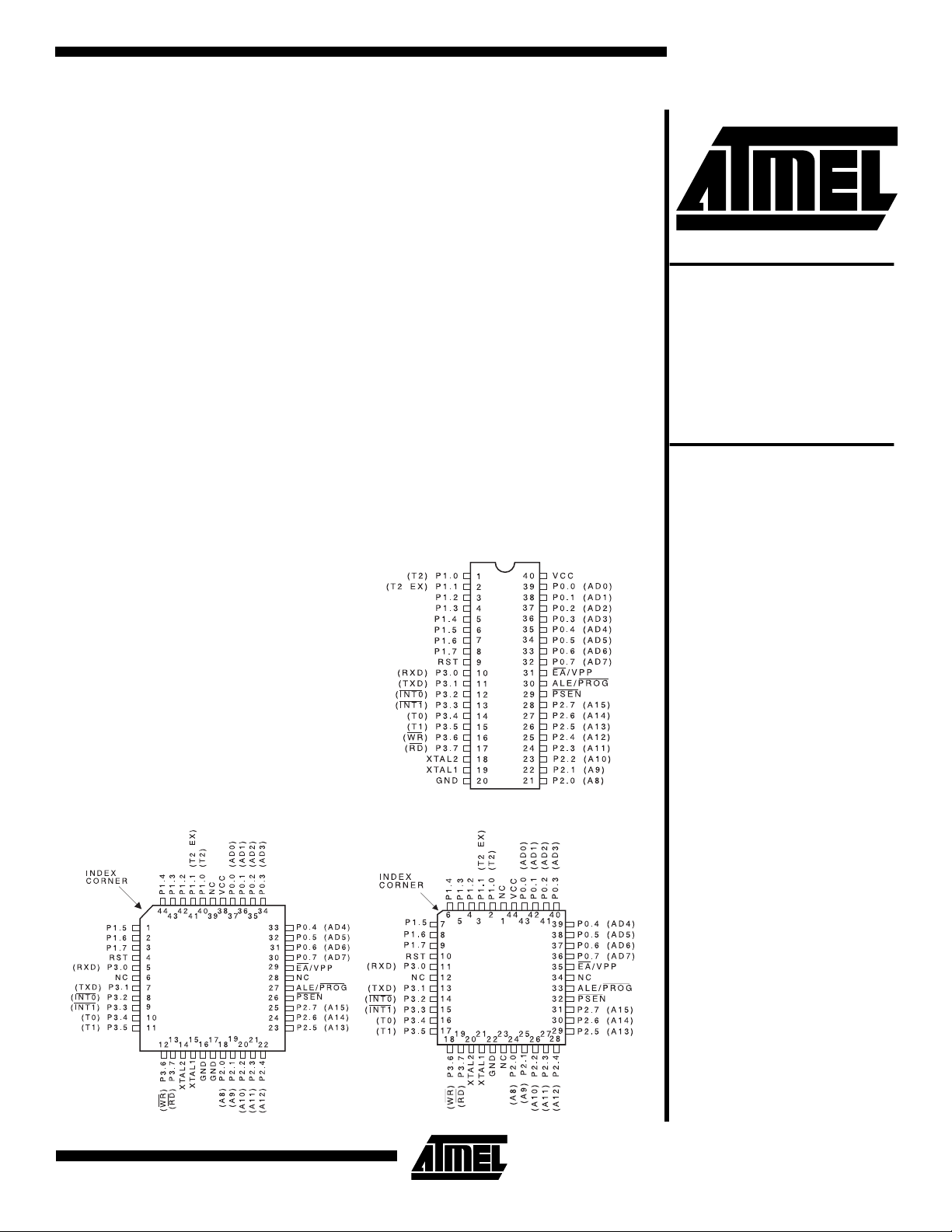
Pin Configurations
PDIP
Microcontroller
with 20K Bytes
Flash
AT89C55
PQFP/TQFP PLCC
0580D-A–12/97
4-169
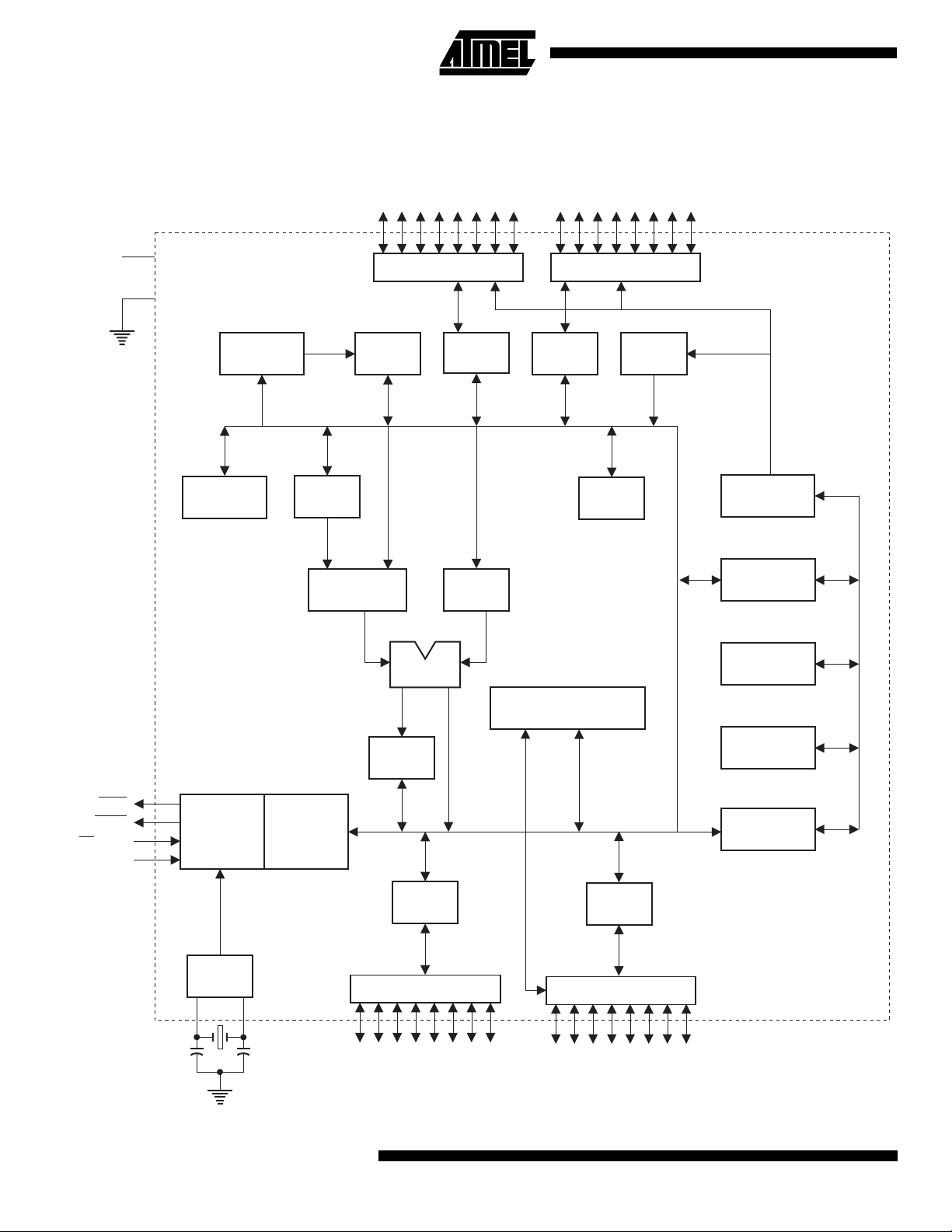
Block Diagram
V
CC
GND
RAM ADDR.
REGISTER
B
REGISTER
P0.0 - P0.7
PORT 0 DRIVERS
RAM
ACC
TMP2 TMP1
PORT 0
LATCH
P2.0 - P2.7
PORT 2 DRIVERS
PORT 2
LATCH
STACK
POINTER
FLASH
PROGRAM
ADDRESS
REGISTER
BUFFER
PSEN
ALE/PROG
EA / V
RST
ALU
INTERRUPT, SERIAL PORT,
AND TIMER BLOCKS
PSW
TIMING
AND
PP
CONTROL
OSC
INSTRUCTION
REGISTER
PORT 1
LATCH
PORT 1 DRIVERS
P1.0 - P1.7
PORT 3
LATCH
PORT 3 DRIVERS
P3.0 - P3.7
PC
INCREMENTER
PROGRAM
COUNTER
DPTR
4-170
AT89C55

AT89C55
The AT89C55 provides the following standard features:
20K bytes of Flash, 256-bytes of RAM, 32 I/O lines, three
16-bit timer/counters, a six-vector two-level interrupt architecture, a full duplex serial port, on- chip oscillator, and
clock circuitry. In addition, the AT89C55 is designed with
static logic for operation down to zero frequency and supports two software selectable powe r saving modes. The
Idle Mode stops the CP U while allowing the RAM,
timer/counters, serial port, and interrupt system to continue
functioning . The Powe r Down Mode saves the RA M contents but freezes the oscillator, disabling all other chip functions until the nex t hardw are r eset . The low -volt age op tion
saves power and operates with a 2.7-volt power supply.
Pin Description
V
CC
Supply voltage.
GND
Ground.
Port 0
Port 0 is an 8-bit open drain bidirectional I/O port. As an
output port, ea ch pin can si nk eight TTL in puts. Whe n 1s
are written to port 0 pins, the pi ns can be used as highimpedance inputs.
Port 0 can also be configured to be the multiplex ed loworder address/data bus during accesses to external program and data memory. In this mode, P0 has internal pullups.
Port 0 also rece ives the code by tes duri ng Flash pr ogramming and outputs the code bytes during program v erification. External pullups are required during program verification.
Port 1
Port 1 is an 8-bit bi directi onal I/ O p ort wit h inter nal pullu ps.
The Port 1 output buffers can sink/source four TTL inputs.
When 1s are writt en to Port 1 pin s, th ey a re pul led high by
the internal pullups and can be used as inputs. As inputs ,
Port 1 pins that are externally being pulled low will source
current (I
In addition, P1.0 and P1.1 can be configured to be th e
timer/counter 2 external count input (P1.0/T2) and the
timer/counter 2 trigger input (P1.1/T2EX), respectively, as
shown in the following table.
Port Pin Alternate Functions
) because of the internal pullups.
IL
Port 2
Port 2 is an 8-bit bidirec tional I/O port wi th interna l pull ups.
The Port 2 output buffers can sink/source four TTL inputs.
When 1s are written to Port 2 pi ns, they are pu lled high by
the internal pullups and can be used as inputs. As inputs,
Port 2 pins that are externally being pulled low will source
current (I
Port 2 emits the high-order address byte during fetches
from external program memory and during accesses to
external data memory that use 16-bit addresses (MOVX @
DPTR). In this application, Port 2 uses strong internal pullups when emitting 1s. During accesses to external data
memory that use 8-bit addresses (MOVX @ RI), Port 2
emits the contents of the P2 Special Function Register.
Port 2 also receives the high-order address bits and some
control signals during Flash programming and verification.
Port 3
Port 3 is an 8-bit bidirec tional I/O port wi th interna l pull ups.
The Port 3 output buffers can sink/source four TTL inputs.
When 1s are written to Port 3 pi ns, they are pu lled high by
the internal pullups and can be used as inputs. As inputs,
Port 3 pins that are externally being pulled low will source
current (I
Port 3 also serves t he functio ns of v arious specia l featu res
of the AT89C55, as shown in the following table.
Port Pin Alternate Functions
P3.0 RXD (serial input port)
P3.1 TXD (serial output port)
P3.2 INT0
P3.3 INT1
P3.4 T0 (timer 0 external input)
P3.5 T1 (timer 1 external input)
P3.6 WR
P3.7 RD
Port 3 also receives the highest-order address bit and
some control sig nals f or Flash programm ing and verific ation.
RST
Reset input. A high on this pin for two machine cycles while
the oscillator is running resets the device.
) because of the internal pullups.
IL
) because of the pullups.
IL
(external interrupt 0)
(external interrupt 1)
(external data memory write strobe)
(external data memory read strobe)
P1.0
P1.1
Port 1 also receives the low-order address bytes during
Flash programming and verification.
T2 (external count input to Timer/Counter 2),
clock-out
T2EX (Timer/Counter 2 capture/reload
trigger and direction control)
4-171

ALE/PROG
Address Latch Enable is an output pulse for latching the
low byte of th e addres s duri ng acce sses to exter nal me mory. This pin is also the program pulse input (PROG
ing Flash programming.
In normal operation, ALE is emitted at a constant rate of
1/6 the oscillator frequency and may be used for external
timing or clocking purposes. Note, however, that one ALE
pulse is skipped during each access to external data memory.
If desired, ALE operation can be disabled by setting bit 0 of
SFR location 8EH. With the bit set, ALE is active only during a MOVX or MOVC instruction. Otherwise, the pin is
weakly pulled high. Setting the ALE-disable bit has no
effect if the microcontroller is in external execution mode.
PSEN
Program Store Enable is the read strobe to external program memory.
When the AT89C55 is executing code from external program memory, PSEN
cycle, except t ha t two PSEN
each access to external data memory.
/V
EA
PP
External Access Enable. EA must be str apped to GND in
order to enable the de vice to fetch co de fro m exte rnal pr ogram memory locations starting at 0000H up to FFFFH.
Note, however, that if lock bit 1 is programmed, EA
internally latched on reset.
should be strapp ed to VCC for internal program execu-
EA
tions.
This pin also receives the 12-volt programming enable voltage (V
XTAL1
Input to the inverting oscillator amplifier and input to the
internal clock operating circuit.
XTAL2
Output from the inverting oscillator amplifier.
) during 12-volt Flash programming.
PP
is activated twice each machine
activations are skipped during
) dur-
will be
User software should not write 1s to these unlisted locations, since they may be used in future products to invoke
new features. In tha t case, the reset or inacti ve values of
the new bits will always be 0.
Timer 2 Registers
registers T2CON (shown in Tabl e 2) and T2MO D (shown
in Table 4) for Timer 2. The register pair (RCAP2H,
RCAP2L) are the Capture/Relo ad regist ers for Time r 2 in
16 bit capture mode or 16-bit auto-reload mode.
Interrupt Registers
in the IE register. Two priorities can be set for each of the
six interrupt sources in the IP register.
Control and status bits are contained in
The individual interrupt enable bits are
Data Memory
The AT89C55 implem ents 256- bytes of on- chip RAM. The
upper 128-bytes occupy a parallel address space to the
Special Function Regi sters. That means the upper 128bytes have the sam e addres ses as the S FR spac e but are
physically separate from SFR space.
When an instruction accesses an internal location above
address 7FH, the address mode used in the instruction
specifies whether the CPU accesses the upper 128-bytes
of RAM or the SFR space. Instructions that use direct
addressing access SFR spac e.
For example, the following direct addressing instruction
accesses the SFR at location 0A0H (which is P2).
MOV 0A0H, #data
Instructions that use indirect addressing access the upper
128-bytes of RAM. For example, the following indirect
addressing instruction, where R0 contains 0A0H, accesses
the data byte at address 0A0H, rather than P2 (whose
address is 0A0H).
MOV @R0, #data
Note that stack operations are examples of indirect
addressing, so the u pper 1 28-by tes of d ata RAM ar e avai lable as stack space.
Special Function Registers
A map of the on-chip memory area called the Specia l
Function Register (SFR) space is shown in Table 1.
Note that not all of the address es are occu pied, and uno ccupied addresses may not be implemen ted on the chip.
Read accesses to these addresses will in general return
random data, and write accesses will have an indeterminate effect.
4-172
AT89C55

AT89C55
Table 1.
0E8H 0EFH
0E0H
0D8H 0DFH
0D0H
0C8H
0C0H 0C7H
0B8H
0B0H
0A8H
0A0H
AT89C55 SFR Map and Reset Values
0F8H 0FFH
0F0H
98H
90H
88H
80H
B
00000000
ACC
00000000
PSW
00000000
T2CON
00000000
IP
XX000000
P3
11111111
IE
0X000000
P2
11111111
SCON
00000000
P1
11111111
TCON
00000000
P0
11111111
T2MOD
XXXXXX00
SBUF
XXXXXXXX
TMOD
00000000
SP
00000111
RCAP2L
00000000
TL0
00000000
DPL
00000000
RCAP2H
00000000
TL1
00000000
DPH
00000000
TL2
00000000
TH0
00000000
TH2
00000000
TH1
00000000
PCON
0XXX0000
0F7H
0E7H
0D7H
0CFH
0BFH
0B7H
0AFH
0A7H
9FH
97H
8FH
87H
4-173

Table 2.
T2CON—Timer/Counter 2 Control Register
T2CON Address = 0C8H Reset Value = 0000 0000B
Bit Addressable
TF2 EXF2 RCLK TCLK EXEN2 TR2 C/T2
Bit 7 6543210
Symbol Function
TF2 Timer 2 overfl ow fl ag set by a Ti mer 2 o v e rflo w and must be cleare d b y softw are . TF 2 will not be set whe n either RCLK
EXF2 Timer 2 external flag set when either a capture or reload is caused by a negative transition on T2EX and EXEN2 = 1.
RCLK Receive cloc k en abl e. When s et, causes the serial port to use Timer 2 o ve rflow pulses f or it s receiv e clo ck in se rial port
TCLK Transmit clock enable. When set, causes the serial port to use Timer 2 overflow pulses for its transmit clock in serial
EXEN2 Timer 2 external enable. When set, allows a capture or reload to occur as a result of a negative transition on T2EX if
TR2 Start/Stop control for Timer 2. TR2 = 1 starts the timer.
C/T2
CP/RL2
= 1 or TCLK = 1.
When Timer 2 interrupt is enabled, EXF2 = 1 will cause the CPU to vector to the Timer 2 interrupt routine. EXF2 must
be cleared by software. EXF2 does not cause an interrupt in up/down counter mode (DCEN = 1).
Modes 1 and 3. RCLK = 0 causes Timer 1 overflow to be used for the receive clock.
port Modes 1 and 3. TCLK = 0 causes Timer 1 overflows to be used for the transmit clock.
Timer 2 is not being used to clock the serial port. EXEN2 = 0 causes Timer 2 to ignore events at T2EX.
Timer or counter select for Timer 2. C/T2 = 0 for timer function. C/T2 = 1 for external event counter (falling edge
triggered).
Capture/Reload selec t. CP/RL2 = 1 c aus es c ap tures to oc cur on n egative tran si tio ns at T2EX if EXEN2 = 1. CP/RL2 =
0 causes automatic reloads to occur when Timer 2 overflows or negative transitions occur at T2EX when EXEN2 = 1.
When either RCLK or TCLK = 1, this bit is ignored and the timer is forced to auto-reload on Timer 2 overflow.
CP/RL2
4-174
AT89C55
AT89C55
Timer 0 and 1
Timer 0 and Timer 1 in the AT89C55 operate the same way
as Timer) and Timer 1 in the AT89C51 and AT89C52. For
further information, see the Microcontroller Data Book, section titled, “Timer/Counters.”
Timer 2
Timer 2 is a 16 bit Timer/Counter that can operate as either
a timer or an event counter. The type of operation is
selected by bit C/T2
Timer 2 has three operating modes: capture, auto-reload
(up or down counting), and baud rate generator. The
modes are selected by bits in T2CON, as shown in Table 3.
Timer 2 consists of two 8- bi t regi st er s, TH2 and TL2. I n the
Timer function, the TL2 r egister is incremented ever y
machine cycle. Since a machine cycle consists of 12 oscillator periods, the count rate is 1/12 of the oscillator frequency.
In the Counter function, the register is incremented in
response to a 1-to-0 transition at its corresponding external
input pin, T2. In thi s func tion, the extern al i nput is sa mpled
during S5P2 of every machin e cycle. When the samples
Table 3.
Timer 2 Operating Modes
RCLK + TCLK CP/RL2 TR2 MODE
0 0 1 16 bit Auto-Re loa d
0 1 1 16 bit Capture
1 X 1 Baud Rate Generator
X X 0 (Off)
in the SFR T2 C ON (sh o w n i n Ta bl e 2).
show a high in one cycle and a low in the next cycle, the
count is incremented. The new count value appears in the
register during S3P1 of the cycle following the one in which
the transition was detected. Since two machine cycles (24
oscillator perio ds ) ar e re qui red to recognize a 1 -to -0 tr an si tion, the maximum count rate is 1/24 of the oscillator frequency. To ensure that a given level is sampled at least
once before it changes, the level should be held for at least
one full machine cycle.
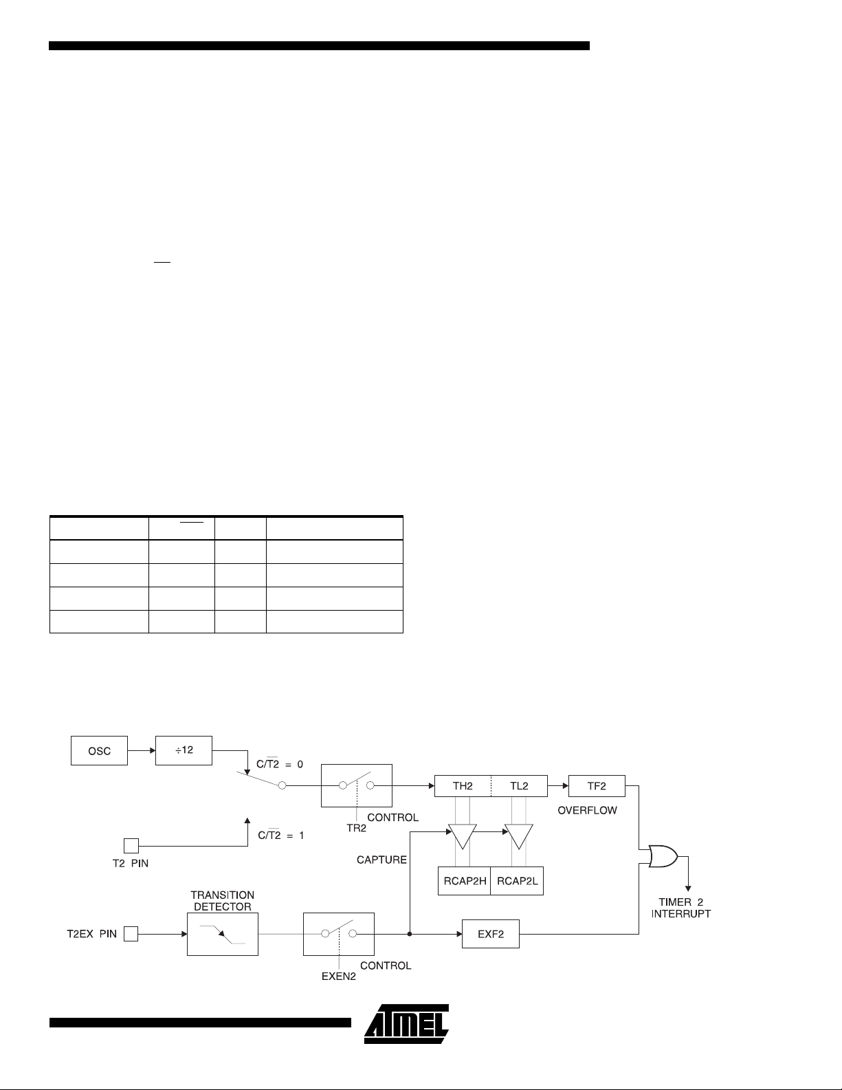
Capture Mode
In the capture mode, two options are selected by bit
EXEN2 in T2CON. If EXEN2 = 0, Timer 2 is a 16 bit timer
or counter which upon overflow sets bit TF2 in T2CON.
This bit can then be used to generate an interrupt. If
EXEN2 = 1, Timer 2 p er forms t he sa me operation, but a 1 to-0 transition at external input T2EX also causes the current value in TH2 and TL2 to be captured into RCAP2H and
RCAP2L, resp ective ly. In addi tion, th e transit ion at T2E X
causes bit EXF2 in T2CON to be set. The EXF2 bit, like
TF2, can generate an interrupt. The capture mode is illustrated in Figure 1.
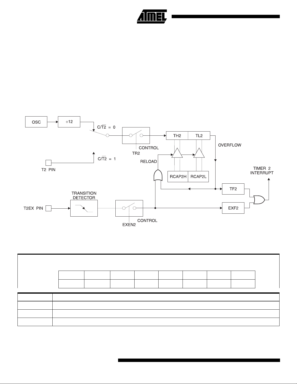
Auto-Reload (Up or Down Counter)
Timer 2 can be programmed to count up or down when
configured in its 16-bit auto-reload mode. This feature is
invoked by the DCEN (Down Counter Enable) bit located in
the SFR T2MOD (see Table 4). Upon reset, the DCEN bit
is set to 0 so that ti mer 2 will defa ult to count u p. When
DCEN is set, Timer 2 can coun t up or down, depend ing on
the value of the T2EX pin.
Figure 2 shows Timer 2 automatically co unting up when
DCEN = 0. In this mod e, two options are selecte d by bit
EXEN2 in T2CON. If EXEN2 = 0, Time r 2 counts up to
0FFFFH and then sets the TF2 bit upon overflow. The overflow also causes the tim er re giste rs to be rel oa ded with the
16 bit value in RCAP2H and RCA P2L. The values in
RCAP2H and RCAP2L are preset by software. If EXEN2 =
Figure 1.
Timer 2 in Capture Mode
4-175
1, a 16 bit reload can be tri gger ed either by an ove rflow or
by a 1-to-0 transition at external input T2EX. This transition
also sets the EXF2 bit. Both th e TF2 and EXF2 bits can
generate an interrupt if enabled.
Setting the DCEN bit enable s Time r 2 to coun t up o r d own,
as shown in Figure 3. In this mode, the T2EX pin controls
the direction of the count. A logic 1 at T2EX makes Timer 2
count up. The timer will overflow at 0FFFFH and set the
TF2 bit. This over flow also causes the 16 bi t value in
RCAP2H and RCAP2L to be reloaded into the timer registers, TH2 and TL2, respectively.
A logic 0 at T2EX makes Timer 2 count down. The timer
underflows when TH2 and TL2 equal the values stor ed in
RCAP2H and RCAP2L. The underflow sets the TF2 bit and
causes 0FFFFH to be reloaded into the timer registers.
The EXF2 bit toggles whenever Timer 2 overflows or
underflows and can be used as a 17th bit of resolution. In
this operating mode, EXF2 does not flag an interrupt.
Figure 2.
Timer 2 Auto Reload Mode (DCEN = 0)
Table 4
4-176
. T2MOD—Timer 2 Mode Control Register
T2MOD Address = 0C9H Reset Value = XXXX XX00B
Not Bit Addressable
— —————T20EDCEN
Bit 7 6543210
Symbol Function
— Not implemented, reserved for future use.
T20E Timer 2 Output Enable bit.
DCEN When set, this bit allows Timer 2 to be configured as an up/down counter.
AT89C55

AT89C55
Figure 3.
OSC
Timer 2 Auto Reload Mode (DCEN = 1)
12
÷
T2 PIN
C/T2 = 0
TR2
C/T2 = 1
(DOWN COUNTING RELOAD VALUE)
0FFH0FFH
OVERFLOW
TH2 TL2
CONTROL
RCAP2LRCAP2H
(UP COUNTING RELOAD VALUE)
TOGGLE
EXF2
TF2
TIMER 2
INTERRUPT
COUNT
DIRECTION
1=UP
0=DOWN
T2EX PIN
Figure 4.
Timer 2 in Baud Rate Generator Mode
4-177

Baud Rate Generator
Timer 2 is sel ected as the baud rat e generat or by settin g
TCLK and/or RCLK in T2CON (Table 2). Note that the baud
rates for transmit and receive can be different if Timer 2 is
used for the receiver or tra nsmitter an d Timer 1 is used for
the other function. Setting RCLK and/or TCLK puts Timer 2
into its baud rate generator mode, as shown in Figure 4.
The baud rate generator mo de is simila r to the auto-reloa d
mode, in that a rollover in TH2 causes the Timer 2 registers
to be reloaded with the 16 bit value in registers RCAP2H
and RCAP2L, which are preset by software.
The baud rates in Mo des 1 and 3 are de termined by Timer
2’s overflow rate according to the following equation.
Modes 1 and 3 Baud Rates
The Timer can be configured for either timer or counter
operation. In most applicatio ns, it is c onfigured for ti mer
operation (CP/T2
= 0). The timer op eration i s different for
Timer 2 when it is used as a baud rate generator. Normally,
as a timer, it increments ev ery machine cy cle (at 1/12 the
oscillator frequency) . As a baud rate ge nerat or, howeve r, it
increments every state time (at 1/2 the oscillator frequency). The baud rate formula is given below.
Timer 2 Overflow Rate
------------------------------------------------------------=
16
Modes 1 and 3
---------------------------------------
Baud Rate
--------------------------------------------------------------------------------------------------=
32 655536 RCAP2H,RCAP2L
Oscillator Frequency
)(–[]×
where (RCAP2H, RCAP2L) is the content of RCAP2H and
RCAP2L taken as a 16 bit unsigned integer.
Timer 2 as a baud rate generator is shown in Figure 4. This
figure is valid only if RCLK or TCLK = 1 in T2CON. Note
that a rollover in TH2 does not set TF2 and will not generate an interrupt. Note too, that if EXEN2 is set, a 1-to-0
transition in T2EX wil l se t EXF2 but will not cau se a reloa d
from (RCAP2H, RCAP2L) to (T H2, TL2). Thu s when Timer
2 is in use as a baud rate ge nerato r, T2EX ca n be used as
an extra external interrupt.
Note that when Timer 2 is running (TR2 = 1) as a timer in
the baud rate gene rator m ode, TH2 or T L2 sh ould n ot be
read from or written to. Under these conditions, the Timer is
incremented every state time, and the results of a read or
write may not be accurate. The RCAP2 registers may be
read but should not be written to, be cause a write might
overlap a r eload a nd caus e wr ite an d/o r re load erro rs. Th e
timer should be turned off (clear TR2) before accessing the
Timer 2 or RCAP2 registers.
Figure 5.
Timer 2 in Clock-Out Mode
4-178
AT89C55

Programmable Clock Out
A 50% duty cycle clock can be programmed to come out on
P1.0, as shown in Figure 5. This pin, besides being a regular I/O pin, has two a lternate functions. It c an be programmed to input the ex ternal clock for Timer/Count er 2 o r
to output a 50% duty cycle clo ck ranging from 61 Hz to 4
MHz at a 16
MHz operating frequency.
To configure the Timer/Counter 2 as a clock generator, bit
(T2CON.1) must be cleared and bit T2OE (T2MOD.1)
C/T2
must be set. Bit TR2 (T2CON.2) starts and stops the timer.
The clock-out frequency depends on the oscillator frequency and the re load value of Timer 2 capt ure registe rs
(RCAP2H, TCAP2L), as shown in the following equation:
Clock-Out Frequency
Oscillator Frequency
----------------------------------------------------------------------------------------------=
4 655536 RCAP2H,RCAP2L)
(–[]×
In the clock-out mode, Timer 2 roll-overs will not generate
an interrupt. This behavior is similar to when Timer 2 is
used as a baud-rate generator. It is possible to use Timer 2
as a baud-rate generator and a clock generator si multaneously. Not e, howeve r, that the ba ud-rate and clock-o ut
frequencies cann ot be determin ed indepen dently fr om one
another since they both use RCAP2H and RCAP2L.
UART
The UART in the AT89C55 operates the same way as the
UART in the AT89C51 and AT89C52. For further information, see the Microcontroller Data Book, section titled,
“Serial Interface.”
AT89C55
Table 5.
Symbol Position Function
EA IE.7
— IE.6 Reserved.
ET2 IE.5 Timer 2 interrupt enable bit.
ES IE.4 Serial Port interrupt enable bit.
ET1 IE.3 Timer 1 interrupt enable bit.
EX1 IE.2 External interrupt 1 enable bit.
ET0 IE.1 Timer 0 interrupt enable bit.
EX0 IE.0 External interrupt 0 enable bit.
User software should never write 1s to unimplemented bits,
because they may be used in future AT89 products.
Figure 6.
Interrupt Enable (IE) Register
(MSB) (LSB)
EA — ET2 ES ET1 EX1 ET0 EX0
Enable Bit = 1 enables the interrupt.
Enable Bit = 0 disables the interrupt.
Disables all interrupts . If EA = 0, no
interrupt is acknowledged. If EA =
1, each interrupt source is
individually enabled or disabled by
setting or clearing its enab le bit.
Interrupt Sources
Interrupts
The AT89C55 has a total of six interrupt vectors: two external interrupts (INT0
ers 0, 1, and 2), and the serial port interrupt. These interrupts are all shown in Figure 6.
Each of these interrupt sources can be individually enabled
or disabled by setting or clearing a bit in Special Function
Register IE. IE also contains a global disable bit, EA, which
disables all interrupts at once.
Note that Table 5 shows that bit position IE.6 is unimplemented. In the AT89C51 and AT89LV51, bit position IE.5 is
also unimplemented. User software should not write 1s to
these bit posit ions, si nce th ey may be used in future AT89
products.
Timer 2 interrupt is generated by the logical OR of bits TF2
and EXF2 in register T2CON. Neither of these flags is
cleared by hardware when the service r outine is vector ed
to. In fact, the serv ice routine may hav e to determine
whether it was TF2 or EXF2 that gen erated the in terrupt,
and that bit will have to be cleared in software.
and INT1), three timer interrupts (Tim-
The Timer 0 and Timer 1 flags, TF0 and TF1, are set at
S5P2 of the cycle in which the timers overflow. The values
are then polled by the circuitry in the next cycle. However,
4-179

the Timer 2 flag, TF2, is set at S2P2 and is polled in the
same cycle in which the timer ove rflows. For further infor mation, see the Microcontroller Data Book, sectio n titled
“Interrupts.”
Oscillator Characteristics
XTAL1 and XTAL2 are the input and output, resp ectively,
of an inverting amplifier that can be confi gured for use as
an on-chip oscillator, as shown in Figure 7. Either a quartz
crystal or ceramic resonator may be used. To drive the
device from an external clock source, XTAL2 should be left
unconnected while XTAL1 is driven, as shown in Figure 8.
There are no requirements on the duty cycle of the external
clock signal, since the input to the internal clocking circuitry
is through a divide-by-two flip-flop, but minimum and maximum voltage high and low time specifications must be
observed.
Idle Mode
In idle mode, the CPU puts itself to sleep while all the onchip peripherals remain active. The mode is invoked by
software. The content of the on-chip RAM and all the special functions registers remain unchanged during this
mode. The idle mode can be terminated by any en abled
interrupt or by a hardware reset.
Note that when idle mode is terminated by a hardware
reset, the device norm ally resumes program execution
from where it left off, up to two machine cycles before the
internal reset algorithm takes control. On-chip hardware
inhibits access to internal RAM in this event, but access to
the port pins is not inhibited. To eliminate the possibility of
an unexpected write to a port pin when idle mode is terminated by a reset, the instruction following the one that
invokes idle m ode s hou ld not write to a po rt pin or to external memory.
Figure 7.
Note: C1,C2 = ± 30 pF for Crystals
Figure 8
Oscillator Connections
=
. External Clock Drive Configuration
40 pF for Ceramic Resonators
±
Status of External Pins During Idle and Power Down Modes
Mode Program Memory ALE PSEN PORT0 PORT1 PORT2 PORT3
Idle Internal 1 1 Data Data Data Data
Idle External 1 1 Float Data Address Data
Power Down Internal 0 0 Data Data Data Data
Power Down External 0 0 Float Da ta Data Data
4-180
AT89C55

AT89C55
Power Down Mode
In the power do wn mode , the osci llat or is sto pped, and the
instruction that invokes power down is the last instruction
executed. The on-chip RAM and Special Function Registers retain their values unti l the powe r down m od e is te rminated. The only exit from power down is a hardware reset.
Reset redefines the SFRs but does not c hange th e on-chi p
RAM. The reset should not be activated before V
restored to its normal operating level and must be held
active long enough to allow the oscillator to re st ar t an d sta-
CC
Program Memory Lock Bits
The AT89C55 has th ree lock bits that c an be left unprogrammed (U) or can be programmed (P) to obtain the additional fea tures listed in the following table.
When lock bit 1 is programmed, the logic level at the EA
is sampled and latche d during rese t. If the device is powered up without a reset, the latch initializes to a random
is
value and holds that value until reset is activated. The
latched value of EA
at that pin in order for the device to function properly.
bilize.
Lock Bit Protection Modes
Program Lock Bits
LB1 LB2 LB3 Protec tion Type
1 U U U No program lock features.
2PUU
3 P P U Same as mode 2, but verify is also disabled.
4 P P P Same as mode 3, but external execution is also disabled.
MOVC instructi ons execu ted from e x ternal prog r am m emory are disa b led fr om fetching cod e b yte s
from internal memory, EA
memory is disabled.
is sampled and latched on reset, and further programming of the Flash
pin
must agree w ith th e cur rent l ogic le vel
Programming the Flash
The AT89C55 is normally shipped with the on-chip Flash
memory array in the erased state (that is, contents = FFH)
and ready to be programmed. T he programm ing interface
accepts either a hi gh-voltage (12-v olt) or a low-vo ltage
) program enable signal. The low voltage programming
(V
CC
mode provides a conven ient wa y to pro gram the A T89C5 5
inside the user’s system, whi le the high -voltage programming mode is compatible with conventional third party
Flash or EPROM programmers.
The AT89C55 is shipped with either the high-voltage or
low-voltage programming mode enabled. The r espective
top-side marking and device signat ure codes ar e listed in
following table.
Top-Side Mark
Signature
VPP = 12V V
AT89C55 AT89C55
xxxx xxxx-5
yyww yyww
(030H) = 1EH (030H) = 1EH
(031H) = 55H (031H) = 55H
(032H) = FFH (032H) = 05H
PP
= 5V
The AT89C55 code memory array is programmed byte-bybyte in either programming mode.
To program any nonblank byte in the on- c hip Fl ash M emo ry , the enti re m emo r y
must be erased using the Chip Erase Mode.
Programming Algorithm:
Before programming the
AT89C55, the address, data and control signals should be
set up according to the Flash programming mode table and
Figures 9 and 10. T o program the AT89C55 , take the following steps:
1. Input the desired memory location on the address lines.
2. Input the appropriate data byte on the data lines.
3. Activate the correct combination of control signals.
4. Raise EA
/VPP to 12V for the high-voltage programming
mode.
5. Pulse ALE/PROG
once to program a byte in the Flas h
array or the lock bits. The byte-write cycle is self-tim ed
and typically takes no more tha n 1.5 ms. Rep eat step s
1 through 5, changing the address and data for the
entire array or until the end of the object file is reached.
4-181

Data
Polling:
The AT89C55 features Data
Polling to indicate the end of a write cycle. During a write cycle, an
attempted read of the l a st b yt e w r it t en w i ll r esu lt i n t h e c o mplement of the written da ta on PO. 7. Once the wr ite cycle
has been completed, true data is valid on all outputs, and
the next cycle may begin . Data
Polling may begi n any time
after a write cycle has been initiated.
Ready/Busy
be monitored by the RDY/B SY
:
The progress of byte programming can also
output signal. P 3.4 i s p ul led
low after ALE goes high during programming to indicate
. P3.4 is pulled high again when programming is
BUSY
done to indicate READY.
Program Verify:
If lock bits LB1 and LB2 have not been
programmed, the programmed code data can be read back
via the address an d data lin es for v erificatio n. The lo ck bi ts
cannot be verified direc tly. Verification of the lock bits is
achieved by observing that their features are enabled.
Chip Erase:
The entire Flash array is erased electrically
by using the prop er combinat ion of c ontrol signals and by
holding ALE/PROG
low for 10 ms. The code array is written
with all 1s. The chip erase operation mus t be executed
before the code memory can be reprogrammed.
Reading the Signature Bytes:
The signature bytes are
read by the same procedure as a normal v erification of
locations 030H, 031H, and 0 32H, except that P3. 6 and
P3.7 must be pulled to a logic low. The va lues returned are
as follows.
(030H) = 1EH indicates manufactured by Atmel
(031H) = 55H indicates 89C55
(032H) = FFH indicates 12V programming
(032H) = 05H indicates 5V programming
Programming Interface
Every code byte in the Flash array can be written, and the
entire array can be erased, by using the appropriate combination of control signals. The write oper ation cycle i s selftimed and once initiated, will automatically time itself to
completion.
All major programm ing vend ors offer worldwide s upport for
the Atmel microcontroller series. Please contact your local
programming vendor for the appropriate software revision.
Figure 9.
SEE FLASH
PROGRAMMING
MODES TABLE
*Programming address line A14 (P3.0) is not the same as the external
memory address line A14 (P2.6)
Programming the Flash Memory
ADDR.
0000H/4FFFH
3-33 MHz
A0-A7
A8 - A13
A14*
P1
P2.0 - P2.5
P3.0
P2.6
P2.7
P3.6
P3.7
XTAL2 EA
XTAL 1
GND
AT89C55
PSEN
V
CC
P0
ALE
RST
+5V
PGM
DATA
PROG
V/V
I H PP
V
I H
Figure 10.
ADDR.
0000H/4FFFH
SEE FLASH
PROGRAMMING
MODES TABLE
3-33 MHz
Verifying the Flash Memory
AT89C55
A0-A7
A8 - A13
P1
P2.0 - P2.5
P3.0A14*
P2.6
P2.7
P3.6
P3.7
XTAL 2 EA
XTAL 1
GND
V
CC
P0
ALE
RST
PSEN
+5V
PGM DATA
(USE 10K
PULLUPS)
V
I H
V
I H
4-182
AT89C55

Flash Programming Modes
AT89C55
Mode RST PSEN ALE/PROG EA/V
Write Code Data H L H/12V L H H H
Read Code Data H L H H L L H H
Write Lock
Chip Erase
Read Signature Byte H L H H L L L L
Note: 1. Chip Erase requires a 10-ms PROG pulse.
Bit-1
Bit-2
Bit-3
H L H/12V HHHH
HL H/12V HHLL
HL H/12V HLHL
HL H/12V HLLL
(1)
PP
P2.6 P2.7 P3.6 P3.7
4-183

Flash Programming and Verification Characteristics
TA = 0°C to 70°C, VCC = 5.0V ± 10%
Symbol Parameter Min Max Units
(1)
V
PP
(1)
I
PP
1/t
CLCL
t
AVGL
t
GHAX
t
DVGL
t
GHDX
t
EHSH
t
SHGL
(1)
t
GHSL
t
GLGH
t
AVQV
t
ELQV
t
EHQZ
t
GHBL
t
WC
Note: 1. Only used in 12-volt programming mode.
Programming Enable Voltage 11.5 12.5 V
Programming Enable Current 1.0 mA
Oscillator Frequency 3 33 MHz
Address Setu p to PROG Low 48t
Address Hold After PROG 48t
Data Setup to PROG Low 48t
Data Hold After PROG 48t
P2.7 (ENABLE) High to V
PP
48t
CLCL
CLCL
CLCL
CLCL
CLCL
VPP Setup to PROG Low 10 µs
VPP Hold After PROG 10 µs
PROG Width 1 110 µs
Address to Data Valid 48t
ENABLE Low to Data Valid 48t
Data Float After ENABLE 048t
CLCL
CLCL
CLCL
PROG High to BUSY Low 1.0 µs
Byte Write Cycle Time 2.0 ms
4-184
AT89C55

AT89C55
Flash Programming and Verification Waveforms - High Voltage Mode (VPP = 12V)
Flash Programming and Verification Waveforms - Low Voltage Mode (VPP = 5V)
4-185

Absolute Maximum Ratings*
Operating Temperature................................. -55°C to +125°C
*NOTICE: Stresses beyond those listed under “Absolute
Maximum Ratings” may cause permanent dam-
Storage Temperature..................................... -65°C to +150°C
age to the device. This is a stre ss rating only and
functional oper ation of the de v ice at these or any
Voltage on Any Pin
with Respect to Ground.....................................-1.0V to +7.0V
other conditions beyond those indicated in the
operational sections of this specification is not
implied. Exposure to absolute maximum rating
Maximum Operating Voltage.............................................6.6V
conditions f or exte nded periods ma y affec t device
reliability.
DC Output Current...................................................... 15.0 mA
DC Characteristics
The values shown in this table are valid for TA = -40°C to 85°C and VCC = 5.0V ± 20%, unless otherwise noted.
Symbol Parameter Condition Min Max Units
V
IL
V
IL1
V
IH
V
IH1
V
OL
V
OL1
V
OH
V
OH1
I
IL
I
TL
I
LI
RRST R eset Pu lldown Resistor 50 300 k
C
IO
I
CC
Input Low Voltage (Except EA)-0.50.2 V
Input Low Voltage (EA)-0.50.2 V
- 0.1 V
CC
- 0.3 V
CC
Input High Voltage (Except XTAL1, RST) 0.2 VCC + 0.9 VCC + 0.5 V
Input High Voltage (XTA L1, RST) 0.7 V
Output Low Voltage
(Ports 1, 2, 3)
Output Low Voltage
(Port 0, ALE, PSEN)
Output High Voltage
(Ports 1, 2, 3, ALE, PSEN
Output High Voltage
(Port 0 in External Bus Mode)
Logical 0 Input Current
(Ports 1, 2, 3)
(1)
(1)
)
I
= 1.6 mA 0.45 V
OL
I
= 3.2 mA 0.45 V
OL
I
= -60 µA, VCC = 5V ± 10% 2.4 V
OH
I
= -25 µA 0.75 V
OH
I
= -10 µA0.9 V
OH
I
= -800 µA, VCC = 5V ± 10% 2.4 V
OH
I
= -300 µA 0.75 V
OH
I
= -80 µA0.9 V
OH
= 0.45V -50
V
IN
CC
CC
CC
CC
CC
VCC + 0.5 V
Logical 1 to 0 Transition Current (Ports 1, 2, 3) VIN = 2V, VCC = 5V ± 10% -650
Input Leakage Current
(Port 0, EA
)
0.45 < V
< V
IN
CC
±
10
Pin Capacitance Test Freq. = 1 MHz, TA = 25°C 10 pF
Active Mode, 12 MHz 25 mA
Power Supply Current
Idle Mode, 12 MHz 6.5 mA
Power Down Mode
(2)
VCC = 6V 100
V
= 3V 40
CC
V
V
V
V
µ
A
µ
A
µ
A
Ω
µ
A
µ
A
Notes: 1. Under steady state (non-transient) conditions, IOL must be external ly limited as follows: Maximum IOL per port pin: 10 mA.
Maximum I
per 8-bit port: Port 0: 26 mA, Ports 1, 2, 3: 15 mA. Maximum tota l IOL for all out put pins: 71 mA. If I
OL
the test condition, V
may exceed the related specification. Pins are not guaranteed to sink current greater than the listed
OL
exceeds
OL
test conditions.
2. Minimum V
4-186
for Power Down is 2V.
CC
AT89C55

AT89C55
AC Characteristics
Under operating conditions, load capacitance for Port 0, ALE/PROG, and PSEN = 100 pF; load capacitance for all other
outputs = 80 pF.
External Program and Data Memory Characteristics
Symbol Parameter Varia b le Os cill ator Units
Min Max
1/t
CLCL
t
LHLL
t
AVLL
t
LLAX
t
LLIV
t
LLPL
t
PLPH
t
PLIV
t
PXIX
t
PXIZ
t
PXAV
t
AVIV
t
PLAZ
t
RLRH
t
WLWH
t
RLDV
t
RHDX
t
RHDZ
t
LLDV
t
AVDV
t
LLWL
t
AVWL
t
QVWX
t
QVWH
t
WHQX
t
RLAZ
t
WHLH
Oscillator Frequency 0 33 MHz
ALE Pulse Width 2t
Address Valid to ALE Low t
Address Hold After ALE Low t
ALE Low to Valid Instruction In 4t
ALE Low to PSEN Low t
PSEN Pulse Width 3t
PSEN Low to Valid Instruction In 3t
- 40 ns
CLCL
- 13 ns
CLCL
- 20 ns
CLCL
- 65 ns
CLCL
- 13 ns
CLCL
- 20 ns
CLCL
- 45 ns
CLCL
Input Instruction Hold After PSEN 0ns
Input Instruction Float After PSEN t
PSEN to Address Valid t
- 8 ns
CLCL
Address to Valid Instruction In 5t
- 10 ns
CLCL
- 55 ns
CLCL
PSEN Low to Address Float 10 ns
RD Pulse Width 6t
WR Pulse Width 6t
RD Low to Valid Data In 5t
- 100 ns
CLCL
- 100 ns
CLCL
- 90 ns
CLCL
Data Hold After RD 0ns
Data Float After RD 2t
ALE Low to Valid Data In 8t
Address to Valid Data In 9t
ALE Low to RD or WR Low 3t
Address to RD or WR Low 4t
Data Valid to WR Transition t
Data Valid to WR High 7t
Data Hold After WR t
- 50 3t
CLCL
- 75 ns
CLCL
- 20 ns
CLCL
- 120 ns
CLCL
- 20 ns
CLCL
- 28 ns
CLCL
- 150 ns
CLCL
- 165 ns
CLCL
+ 50 ns
CLCL
RD Low to Address Float 0 ns
RD or WR High to ALE High t
- 20 t
CLCL
+ 25 ns
CLCL
4-187

External Program Memory Read Cycle
External Data Memory Read Cycle
4-188
AT89C55

External Data Memory Write Cycle
AT89C55
External Clock Drive Waveforms
Exter nal Clock Drive
Symbol Parameter M in Max Units
1/t
CLCL
t
CLCL
t
CHCX
t
CLCX
t
CLCH
t
CHCL
Oscillator Frequency 0 33 MHz
Clock Period 30 ns
High Time 12 ns
Low Time 12 ns
Rise Time 20 ns
Fall Time 20 ns
4-189

Serial Port Timing: Shift Register Mode Test Conditions
The values in this table are valid for VCC = 5.0V ± 20% and Load Capacitance = 80 pF.
Symbol Parameter Min Max Units
t
XLXL
t
QVXH
t
XHQX
t
XHDX
t
XHDV
Serial Port Clock Cycle Time 12t
Output Data Setup to Clock Rising Edge 10t
Output Data Hold After Clock Rising Edge 2t
Input Data Hold After Clock Rising Edge 0 ns
Clock Rising Edge to Input Data Valid 10t
CLCL
- 133 ns
CLCL
- 117 ns
CLCL
- 133 ns
CLCL
Shift Register Mode Timing Waveforms
ns
AC Testing Input/Output Waveforms
Note: 1. AC Inputs during testing are driven at VCC - 0.5V for a
logic 1 and 0.45V for a logic 0. Timing measurements
are made at V
logic 0.
4-190
min. for a logic 1 and VIL max. for a
IH
AT89C55
(1)
Float Waveforms
Note: 1. For timing purposes, a port pin is no longer
floating when a 100 mV change from load voltage occurs. A port pin begins to float when a
100 mV change from the loaded V
occurs.
(1)
OH/VOL
level

AT89C55
Notes: 1. XTAL1 tied to GND for ICC (power down)
2. Lock bits programmed
4-191

Ordering Information
Speed
(MHz)
16 5V ± 20% AT89C55-16AA
24 5V ± 20% AT89C55-24AC
33 5V ± 10% AT89C55-33AC
Power
Supply Ordering Code Package Operation Range
AT89C55-16JA
AT89C55-16PA
AT89C55-16QA
AT89C55-24JC
AT89C55-24PC
AT89C55-24QC
AT89C55-24AI
AT89C55-24JI
AT89C55-24PI
AT89C55-24QI
AT89C55-33JC
AT89C55-33PC
AT89C55-33QC
44A
44J
40P6
44Q
44A
44J
40P6
44Q
44A
44J
40P6
44Q
44A
44J
40P6
44Q
Automotive
(-40°C to 105°C)
Commercial
(0°C to 70°C)
Industrial
(-40°C to 85°C)
Commercial
(0°C to 70°C)
Package Type
44A 44 Lead, Thin Plastic Gull Wing Quad Flatpack (TQFP)
44J 44 Lead, Plastic J-Leaded Chip Carrier (PLCC)
40P6 40 Lead, 0.600" Wide, Plastic Dual Inline Package (PDIP)
44Q 44 Lead, Plastic Gull Wing Quad Flatpack (PQFP)
4-192
AT89C55
 Loading...