

Page 1

BDTIC www.bdtic.com/ATMEL
Features
• 80C52 Compatible
– 8051 Instruction Compatible
– Six 8-bit I/O Ports (64 Pins or 68 Pins Versions)
– Four 8-bit I/O Ports (44 Pins Version)
– Three 16-bit Timer/Counters
– 256 Bytes Scratch Pad RAM
– 9 Interrupt Sources with 4 Priority Levels
• Integrated Power Monitor (POR/PFD) to Supervise Internal Power Supply
• ISP (In-System Programming) Using Standard V
• 2048 Bytes Boot ROM Contains Low Level Flash Programming Routines and a Default
Serial Loader
• High-speed Architecture
– In Standard Mode:
40 MHz (Vcc 2.7V to 5.5V, both Internal and external code execution)
60 MHz (Vcc 4.5V to 5.5V and Internal Code execution only)
– In X2 mode (6 Clocks/machine cycle)
20 MHz (Vcc 2.7V to 5.5V, both Internal and external code execution)
30 MHz (Vcc 4.5V to 5.5V and Internal Code execution only)
• 64K Bytes On-chip Flash Program/Data Memory
– Byte and Page (128 Bytes) Erase and Write
– 100k Write Cycles
• On-chip 1792 bytes Expanded RAM (XRAM)
– Software Selectable Size (0, 256, 512, 768, 1024, 1792 Bytes)
– 768 Bytes Selected at Reset for T89C51RD2 Compatibility
• On-chip 2048 Bytes EEPROM Block for Data Storage (AT89C51ED2 Only)
– 100K Write Cycles
• Dual Data Pointer
• Variable Length MOVX for Slow RAM/Peripherals
• Improved X2 Mode with Independent Selection for CPU and Each Peripheral
• Keyboard Interrupt Interface on Port 1
• SPI Interface (Master/Slave Mode)
• 8-bit Clock Prescaler
• 16-bit Programmable Counter Array
– High Speed Output
– Compare/Capture
– Pulse Width Modulator
– Watchdog Timer Capabilities
• Asynchronous Port Reset
• Full-duplex Enhanced UART with Dedicated Internal Baud Rate Generator
• Low EMI (Inhibit ALE)
• Hardware Watchdog Timer (One-time Enabled with Reset-Out), Power-off Flag
• Power Control Modes: Idle Mode, Power-down Mode
• Single Range Power Supply: 2.7V to 5.5V
• Industrial Temperature Range (-40 to +85°C)
• Packages: PLCC44, VQFP44, PLCC68, VQFP64
Power Supply
CC
8-bit Flash
Microcontroller
AT89C51RD2
AT89C51ED2
Description
AT89C51RD2/ED2 is high performance CMOS Flash version of the 80C51 CMOS single chip 8-bit microcontroller. It contains a 64-Kbyte Flash memory block for code and
for data.
The 64-Kbytes Flash memory can be programmed either in parallel mode or in serial
mode with the ISP capability or with software. The programming voltage is internally
generated from the standard V
CC
pin.
Rev. 4235I–8051–04/07
1
Page 2

AT89C51RD2/ED2
The AT89C51RD2/ED2 retains all of the features of the Atmel 80C52 with 256 bytes of
internal RAM, a 9-source 4-level interrupt controller and three timer/counters. The
AT89C51ED2 provides 2048 bytes of EEPROM for nonvolatile data storage.
In addition, the AT89C51RD2/ED2 has a Programmable Counter Array, an XRAM of
1792 bytes, a Hardware Watchdog Timer, SPI interface, Keyboard, a more versatile
serial channel that facilitates multiprocessor communication (EUART) and a speed
improvement mechanism (X2 Mode).
The fully static design of the AT89C51RD2/ED2 allows to reduce system power consumption by bringing the clock frequency down to any value, including DC, without loss
of data.
The AT89C51RD2/ED2 has 2 software-selectable modes of reduced activity and an 8bit clock prescaler for further reduction in power consumption. In the Idle mode the CPU
is frozen while the peripherals and the interrupt system are still operating. In the Powerdown mode the RAM is saved and all other functions are inoperative.
The added features of the AT89C51RD2/ED2 make it more powerful for applications
that need pulse width modulation, high speed I/O and counting capabilities such as
alarms, motor control, corded phones, and smart card readers.
Table 1. Memory Size and I/O Pins
Package Flash (Bytes) XRAM (Bytes) Total RAM (Bytes) I/O
PLCC44/VQFP44 64K 1792 2048 34
PLCC68/VQFP64 64K 1792 2048 50
2
4235I–8051–04/07
Page 3
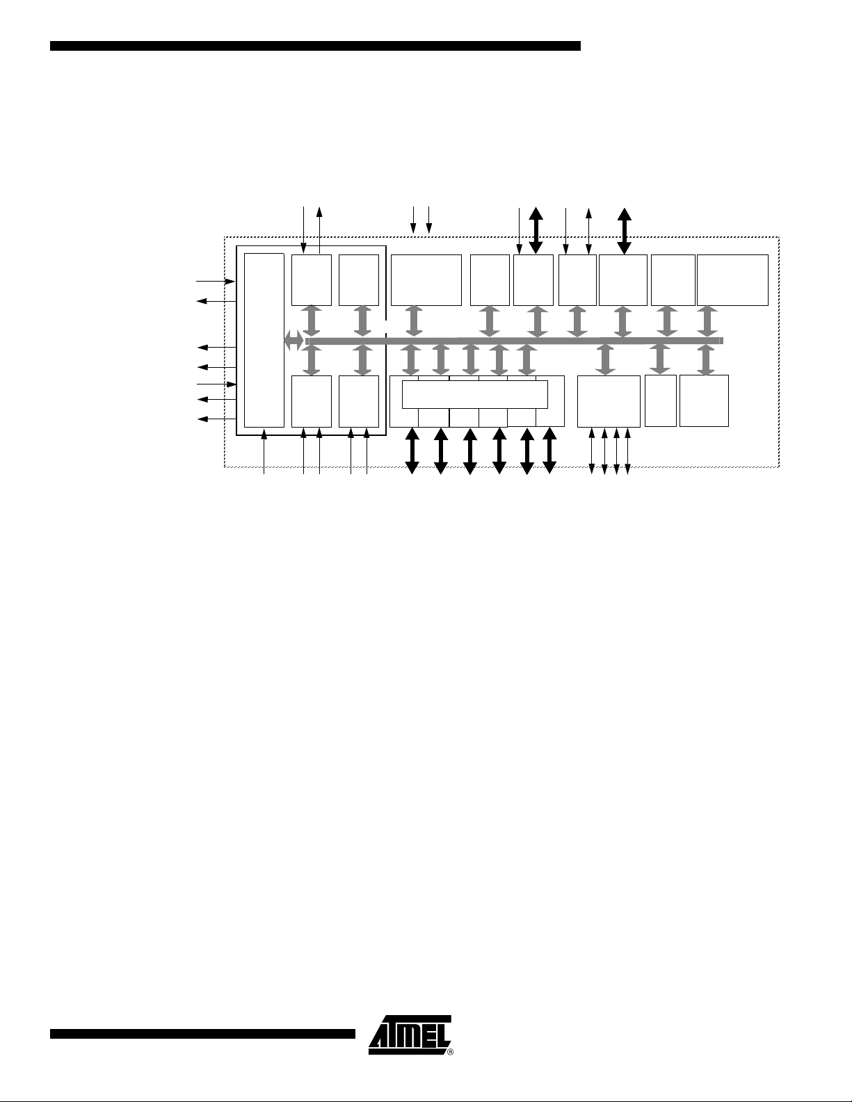
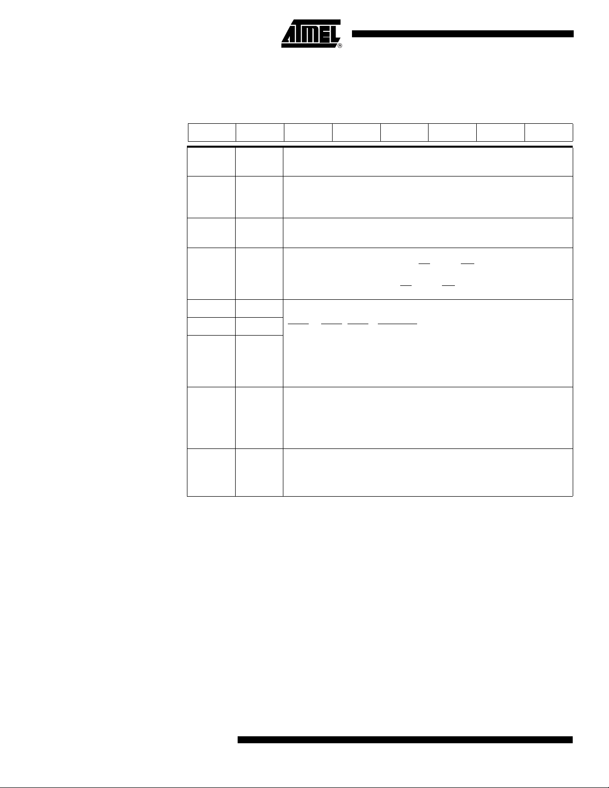
Block Diagram
Timer 0
INT
RAM
256x8
T0
T1
RxD
TxD
WR
RD
EA
PSEN
ALE/
XTALA2
XTALA1 EUART
CPU
Timer 1
INT1
Ctrl
INT0
(2)
(2)
C51
CORE
(2) (2) (2) (2)
Port 0P0Port 1
Port 2
Port 3
P1
P2
P3
XRAM
1792 x 8
IB-bus
PCA
RESET
PROG
Watch
-dog
PCA
ECI
VSS
VCC
(2)(2)
(1)
(1): Alternate function of Port 1
(2): Alternate function of Port 3
(1)
Timer2
T2EX
T2
(1) (1)
Flash
64K x 8
Keyboard
(1)
Keyboard
MISO
MOSI
SCK
SS
Port4
P4
(1)
(1)
(1)
(1)
BOOT
2K x 8
ROM
Regulator
POR / PFD
Port 5
P5
Parallel I/O Ports &
External Bus
SPI
EEPROM*
2K x 8
(AT89C51ED2)
Figure 1. Block Diagram
AT89C51RD2/ED2
4235I–8051–04/07
3
Page 4

AT89C51RD2/ED2
SFR Mapping
The Special Function Registers (SFRs) of the AT89C51RD2/ED2 fall into the following
categories:
• C51 core registers: ACC, B, DPH, DPL, PSW, SP
• I/O port registers: P0, P1, P2, P3, PI2
• Timer registers: T2CON, T2MOD, TCON, TH0, TH1, TH2, TMOD, TL0, TL1, TL2,
RCAP2L, RCAP2H
• Serial I/O port registers: SADDR, SADEN, SBUF, SCON
• PCA (Programmable Counter Array) registers: CCON, CCAPMx, CL, CH, CCAPxH,
CCAPxL (x: 0 to 4)
• Power and clock control registers: PCON
• Hardware Watchdog Timer registers: WDTRST, WDTPRG
• Interrupt system registers: IE0, IPL0, IPH0, IE1, IPL1, IPH1
• Keyboard Interface registers: KBE, KBF, KBLS
• SPI registers: SPCON, SPSTR, SPDAT
• BRG (Baud Rate Generator) registers: BRL, BDRCON
• Clock Prescaler register: CKRL
• Others: AUXR, AUXR1, CKCON0, CKCON1
4
4235I–8051–04/07
Page 5

AT89C51RD2/ED2
Table 2. C51 Core SFRs
Mnemonic Add Name 7 6 5 4 3 2 1 0
ACC E0h Accumulator
B F0h B Register
PSW D0h Program Status Word CY AC F0 RS1 RS0 OV F1 P
SP 81h Stack Pointer
DPL 82h Data Pointer Low Byte
DPH 83h Data Pointer High Byte
Table 3. System Management SFRs
Mnemonic Add Name 7 6 5 4 3 2 1 0
PCON 87h Power Control SMOD1 SMOD0 - POF GF1 GF0 PD IDL
AUXR 8Eh Auxiliary Register 0 DPU - M0 XRS2 XRS1 XRS0 EXTRAM AO
AUXR1 A2h Auxiliary Register 1 - -
CKRL 97h Clock Reload Register - - - - - - - -
CKCKON0 8Fh Clock Control Register 0 - WDTX2 PCAX2 SIX2 T2X2 T1X2 T0X2 X2
CKCKON1 AFh Clock Control Register 1 - - - - - - - SPIX2
ENBOOT
- GF3 0 - DPS
Table 4. Interrupt SFRs
Mnemonic Add Name 7 6 5 4 3 2 1 0
IEN0 A8h Interrupt Enable Control 0 EA EC ET2 ES ET1 EX1 ET0 EX0
IEN1 B1h Interrupt Enable Control 1 - - - - - ESPI KBD
IPH0 B7h Interrupt Priority Control High 0 - PPCH PT2H PHS PT1H PX1H PT0H PX0H
IPL0 B8h Interrupt Priority Control Low 0 - PPCL PT2L PLS PT1L PX1L PT0L PX0L
IPH1 B3h Interrupt Priority Control High 1 - - - - - SPIH KBDH
IPL1 B2h Interrupt Priority Control Low 1 - - - - - SPIL KBDL
Table 5. Port SFRs
Mnemonic Add Name 7 6 5 4 3 2 1 0
P0 80h 8-bit Port 0
P1 90h 8-bit Port 1
P2 A0h 8-bit Port 2
P3 B0h 8-bit Port 3
P4 C0h 8-bit Port 4
4235I–8051–04/07
5
Page 6

AT89C51RD2/ED2
Table 5. Port SFRs
Mnemonic Add Name 7 6 5 4 3 2 1 0
P5 D8h 8-bit Port 5
P5 C7h 8-bit Port 5 (byte addressable)
Table 6. Timer SFRs
Mnemonic Add Name 7 6 5 4 3 2 1 0
TCON 88h Timer/Counter 0 and 1 Control TF1 TR1 TF0 TR0 IE1 IT1 IE0 IT0
TMOD 89h Timer/Counter 0 and 1 Modes GATE1 C/T1# M11 M01 GATE0 C/T0# M10 M00
TL0 8Ah Timer/Counter 0 Low Byte
TH0 8Ch Timer/Counter 0 High Byte
TL1 8Bh Timer/Counter 1 Low Byte
TH1 8Dh Timer/Counter 1 High Byte
WDTRST A6h WatchDog Timer Reset
WDTPRG A7h WatchDog Timer Program - - - - - WTO2 WTO1 WTO0
T2CON C8h Timer/Counter 2 control TF2 EXF2 RCLK TCLK EXEN2 TR2 C/T2# CP/RL2#
T2MOD C9h Timer/Counter 2 Mode - - - - - - T2OE DCEN
RCAP2H CBh
RCAP2L CAh
TH2 CDh Timer/Counter 2 High Byte
TL2 CCh Timer/Counter 2 Low Byte
Timer/Counter 2 Reload/Capture
High Byte
Timer/Counter 2 Reload/Capture
Low Byte
Table 7. PCA SFRs
Mnemo
-nic Add Name 7 6 5 4 3 2 1 0
CCON D8h PCA Timer/Counter Control CF CR CCF4 CCF3 CCF2 CCF1 CCF0
CMOD D9h PCA Timer/Counter Mode CIDL WDTE CPS1 CPS0 ECF
CL E9h PCA Timer/Counter Low Byte
CH F9h PCA Timer/Counter High Byte
CCAPM0
CCAPM1
CCAPM2
CCAPM3
CCAPM4
DAh
PCA Timer/Counter Mode 0
DBh
PCA Timer/Counter Mode 1
DCh
PCA Timer/Counter Mode 2
DDh
PCA Timer/Counter Mode 3
DEh
PCA Timer/Counter Mode 4
ECOM0
ECOM1
ECOM2
ECOM3
ECOM4
CAPP0
CAPP1
CAPP2
CAPP3
CAPP4
CAPN0
CAPN1
CAPN2
CAPN3
CAPN4
MAT0
MAT1
MAT2
MAT3
MAT4
TOG0
TOG1
TOG2
TOG3
TOG4
PWM0
PWM1
PWM2
PWM3
PWM4
ECCF0
ECCF1
ECCF2
ECCF3
ECCF4
6
4235I–8051–04/07
Page 7
AT89C51RD2/ED2
Table 7. PCA SFRs (Continued)
Mnemo
-nic Add Name 7 6 5 4 3 2 1 0
CCAP0H
CCAP1H
CCAP2H
CCAP3H
CCAP4H
CCAP0L
CCAP1L
CCAP2L
CCAP3L
CCAP4L
FAh
PCA Compare Capture Module 0 H
FBh
PCA Compare Capture Module 1 H
FCh
PCA Compare Capture Module 2 H
FDh
PCA Compare Capture Module 3 H
FEh
PCA Compare Capture Module 4 H
EAh
PCA Compare Capture Module 0 L
EBh
PCA Compare Capture Module 1 L
ECh
PCA Compare Capture Module 2 L
EDh
PCA Compare Capture Module 3 L
EEh
PCA Compare Capture Module 4 L
CCAP0H7
CCAP1H7
CCAP2H7
CCAP3H7
CCAP4H7
CCAP0L7
CCAP1L7
CCAP2L7
CCAP3L7
CCAP4L7
CCAP0H6
CCAP1H6
CCAP2H6
CCAP3H6
CCAP4H6
CCAP0L6
CCAP1L6
CCAP2L6
CCAP3L6
CCAP4L6
CCAP0H5
CCAP1H5
CCAP2H5
CCAP3H5
CCAP4H5
CCAP0L5
CCAP1L5
CCAP2L5
CCAP3L5
CCAP4L5
CCAP0H4
CCAP1H4
CCAP2H4
CCAP3H4
CCAP4H4
CCAP0L4
CCAP1L4
CCAP2L4
CCAP3L4
CCAP4L4
CCAP0H3
CCAP1H3
CCAP2H3
CCAP3H3
CCAP4H3
CCAP0L3
CCAP1L3
CCAP2L3
CCAP3L3
CCAP4L3
CCAP0H2
CCAP1H2
CCAP2H2
CCAP3H2
CCAP4H2
CCAP0L2
CCAP1L2
CCAP2L2
CCAP3L2
CCAP4L2
CCAP0H1
CCAP1H1
CCAP2H1
CCAP3H1
CCAP4H1
CCAP0L1
CCAP1L1
CCAP2L1
CCAP3L1
CCAP4L1
CCAP0H0
CCAP1H0
CCAP2H0
CCAP3H0
CCAP4H0
CCAP0L0
CCAP1L0
CCAP2L0
CCAP3L0
CCAP4L0
Table 8. Serial I/O Port SFRs
Mnemonic Add Name 7 6 5 4 3 2 1 0
SCON 98h Serial Control FE/SM0 SM1 SM2 REN TB8 RB8 TI RI
SBUF 99h Serial Data Buffer
SADEN B9h Slave Address Mask
SADDR A9h Slave Address
BDRCON 9Bh Baud Rate Control BRR TBCK RBCK SPD SRC
BRL 9Ah Baud Rate Reload
Table 9. SPI Controller SFRs
Mnemonic Add Name 7 6 5 4 3 2 1 0
SPCON C3h SPI Control SPR2 SPEN SSDIS MSTR CPOL CPHA SPR1 SPR0
SPSTA C4h SPI Status SPIF WCOL SSERR MODF
SPDAT C5h SPI Data SPD7 SPD6 SPD5 SPD4 SPD3 SPD2 SPD1 SPD0
Table 10. Keyboard Interface SFRs
Mnemonic Add Name 7 6 5 4 3 2 1 0
KBLS 9Ch Keyboard Level Selector KBLS7 KBLS6 KBLS5 KBLS4 KBLS3 KBLS2 KBLS1 KBLS0
KBE 9Dh Keyboard Input Enable KBE7 KBE6 KBE5 KBE4 KBE3 KBE2 KBE1 KBE0
KBF 9Eh Keyboard Flag Register KBF7 KBF6 KBF5 KBF4 KBF3 KBF2 KBF1 KBF0
Table 11. EEPROM data Memory SFR (AT89C51ED2 only)
Mnemonic Add Name 7 6 5 4 3 2 1 0
EECON D2h EEPROM Data Control EEE EEBUSY
4235I–8051–04/07
7
Page 8

AT89C51RD2/ED2
Table 12. SFR Mapping
Bit
Addressable Non Bit Addressable
0/8 1/9 2/A 3/B 4/C 5/D 6/E 7/F
Table 12 shows all SFRs with their address and their reset value.
F8h
F0h
E8h
E0h
D8h
D0h
C8h
C0h
B8h
B0h
B
0000 0000
P5 bit
addressable
1111 1111
ACC
0000 0000
CCON
00X0 0000
PSW
0000 0000
T2CON
0000 0000
P4
1111 1111
IPL0
X000 000
P3
1111 1111
CH
0000 0000
CL
0000 0000
CMOD
00XX X000
FCON
XXXX 0000
T2MOD
XXXX XX00
SADEN
0000 0000
IEN1
XXXX X000
CCAP0H
XXXX XXXX
CCAP0L
XXXX XXXX
CCAPM0
X000 0000
EECON
xxxx xx00
RCAP2L
0000 0000
IPL1
XXXX X000
CCAP1H
XXXX XXXX
CCAP1L
XXXX XXXX
CCAPM1
X000 0000
RCAP2H
0000 0000
SPCON
0001 0100
IPH1
XXXX X111
CCAP2H
XXXX XXXX
CCAP2L
XXXX XXXX
CCAPM2
X000 0000
TL2
0000 0000
SPSTA
0000 0000
CCAP3H
XXXX XXXX
CCAP3L
XXXX XXXX
CCAPM3
X000 0000
TH2
0000 0000
SPDAT
XXXX XXXX
CCAP4H
XXXX XXXX
CCAP4L
XXXX XXXX
CCAPM4
X000 0000
P5 byte
Addressable
1111 1111
IPH0
X000 0000
FFh
F7h
EFh
E7h
DFh
D7h
CFh
C7h
BFh
B7h
A8h
A0h
98h
90h
88h
80h
IEN0
0000 0000
P2
1111 1111
SCON
0000 0000
P1
1111 1111
TCON
0000 0000
P0
1111 1111
0/8 1/9 2/A 3/B 4/C 5/D 6/E 7/F
SADDR
0000 0000
SBUF
XXXX XXXX
TMOD
0000 0000
SP
0000 0111
AUXR1
0XXX X0X0
BRL
0000 0000
TL0
0000 0000
DPL
0000 0000
BDRCON
XXX0 0000
TL1
0000 0000
DPH
0000 0000
KBLS
0000 0000
TH0
0000 0000
KBE
0000 0000
TH1
0000 0000
WDTRST
XXXX XXXX
KBF
0000 0000
AUXR
XX00 1000
CKCON1
XXXX XXX0
WDTPRG
XXXX X000
CKRL
1111 1111
CKCON0
0000 0000
PCON
00X1 0000
AFh
A7h
9Fh
97h
8Fh
87h
reserved
8
4235I–8051–04/07
Page 9
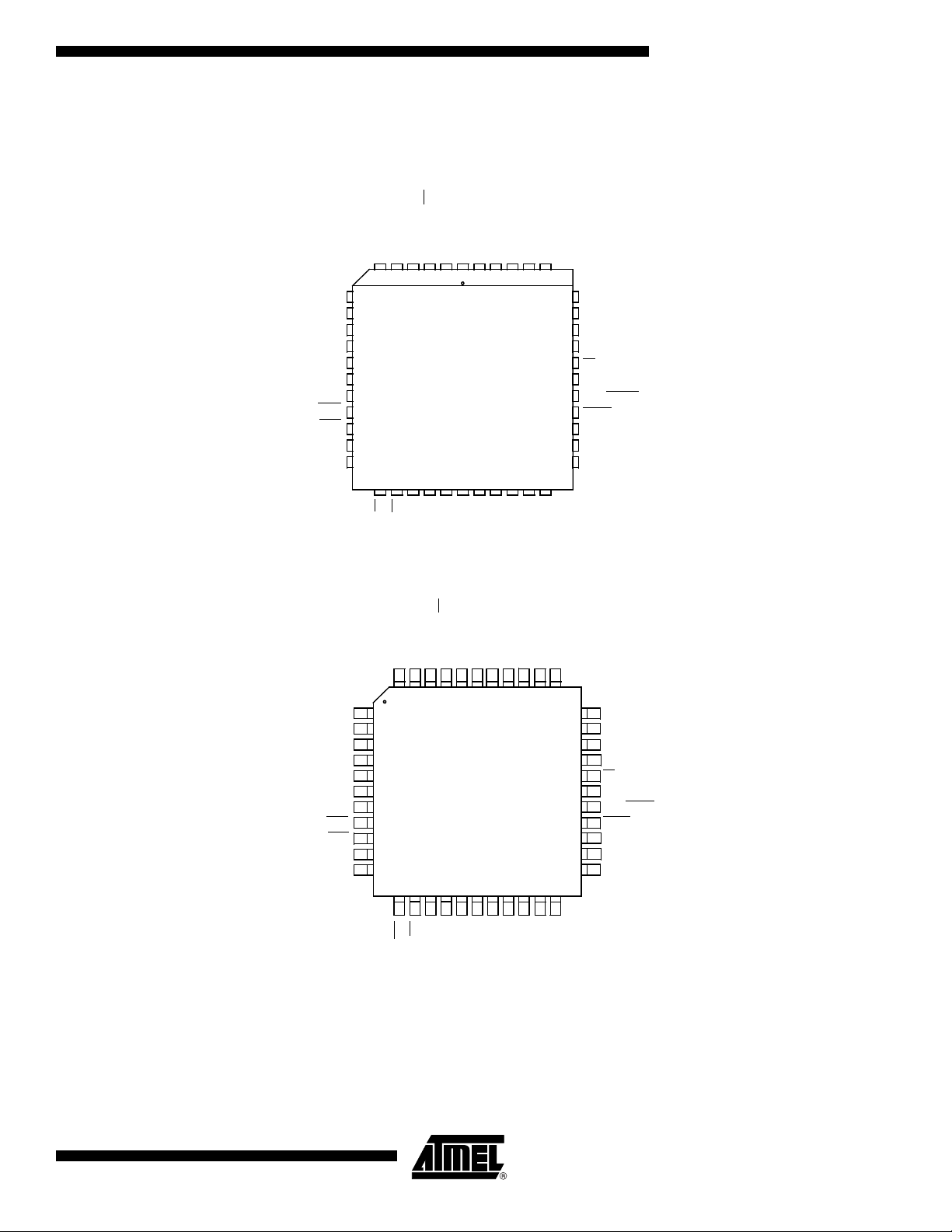
Pin Configurations
43 42 41 40 3944 38 37 36 35 34
P1.4/CEX1
P1.0/T2
P1.1/T2EX/SS
P1.3/CEX0
P1.2/ECI
VCC
P0.0/AD0
P0.2/AD2
P0.3/AD3
P0.1/AD1
P0.4/AD4
P0.6/AD6
P0.5/AD5
P0.7/AD7
ALE/PROG
PSEN
EA
P2.7/A15
P2.5/A13
P2.6/A14
P1.5/CEX2/MISO
P1.6/CEX3/SCK
P1.7/CEX4/MOSI
RST
P3.0/RxD
P3.1/TxD
P3.2/INT0
P3.3/INT1
P3.4/T0
P3.5/T1
P3.6/WR
P3.7/RD
XTAL2
XTAL1
VSS
P2.0/A8
P2.1/A9
P2.2/A10
P2.3/A11
P2.4/A12
NIC*
12 13 17161514 201918 21 22
33
32
31
30
29
28
27
26
25
24
23
AT89C51RD2/ED2
1
2
3
4
5
6
7
8
9
10
11
VQFP44 1.4
NIC*
NIC*
NIC*
PLCC44
AT89C51RD2/ED2
NIC*
NIC*
NIC*
Figure 2. Pin Configurations
AT89C51RD2/ED2
P1.5/CEX2/MISO
P1.6/CEX3/SCK
P1.7/CEx4/MOSI
RST
P3.0/RxD
P3.1/TxD
P3.2/INT0
P3.3/INT1
P3.4/T0
P3.5/T1
7
8
9
10
11
12
13
14
15
16
17
P1.4/CEX1
P1.3/CEX0
5 4 3 2 1 6
P1.0/T2
P1.1/T2EX/SS
P1.2/ECI
VCC
44 43 42 41 40
18 19 23222120 262524 27 28
NIC*
VSS
XTAL2
XTAL1
P3.7/RD
P3.6/WR
P2.0/A8
P0.0/AD0
P2.1/A9
P0.3/AD3
P0.2/AD2
P0.1/AD1
39
P0.4/AD4
38
P0.5/AD5
37
P0.6/AD6
36
P0.7/AD7
35
EA
34
33
ALE/PROG
32
PSEN
31
P2.7/A15
30
P2.6/A14
29
P2.5/A13
P2.2/A10
P2.3/A11
P2.4/A12
4235I–8051–04/07
9
Page 10
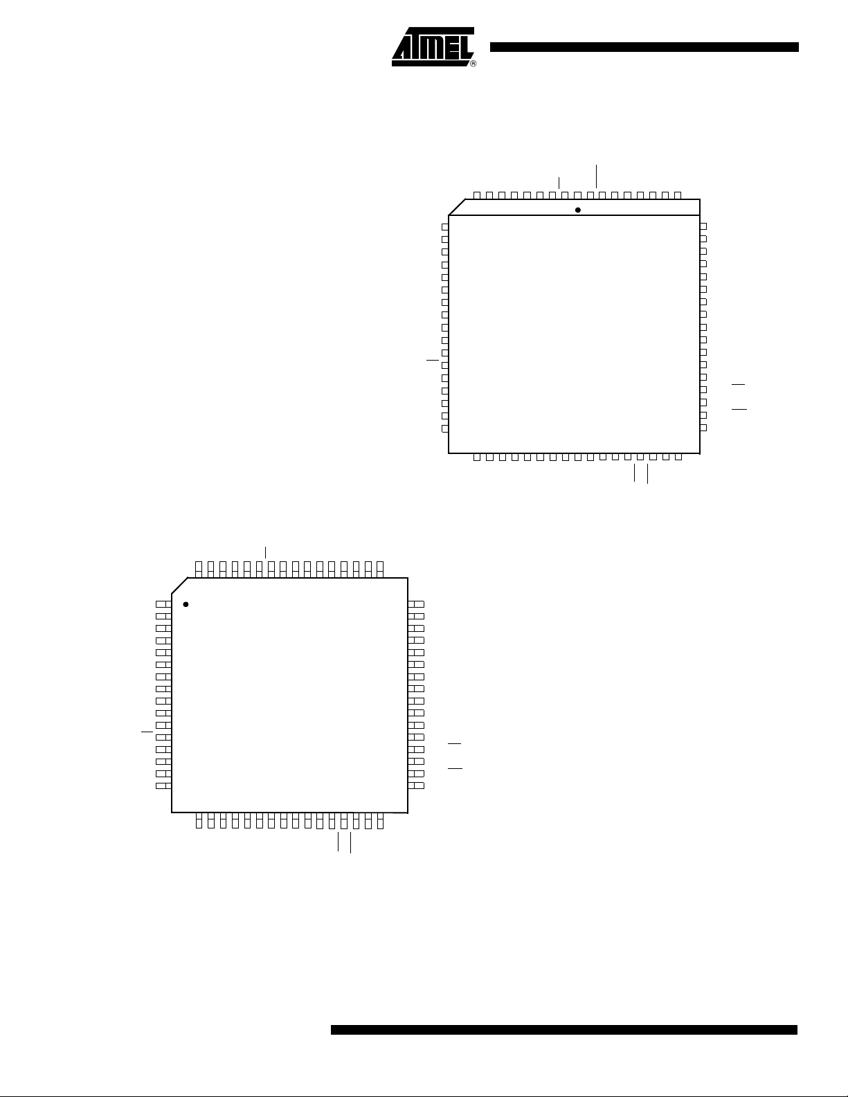
AT89C51RD2/ED2
50
49
48
47
44
45
46
P4.5
P3.7/RD
XTAL2
XTAL1
P4.4
P3.6/WR
P4.3
NIC
NIC
P3.1/TxD
P3.2/INT0
P3.3/INT1
P3.4/T0
P3.5/T1
37383940414243
AT89C51ED2
PLCC68
P0.4/AD4
P5.4
P5.3
P0.5/AD5
P0.6/AD6
NIC
P0.7/AD7EANIC
ALE
P1.6/CEX3/SCK
P1.7/CEX4/MOSI
RST
NIC
NIC
NIC
P3.0/RxD
NIC
NIC
P1.5/CEX2/MISO
60
59
58
57
56
55
54
53
51
52
10
11
12
13
14
15
16
17
19
18
272829303132333435
36
98765
321
68
P5.0
P2.4/A12
P2.3/A11
P4.7
P2.2/A10
P4.6
P2.0/A8
P2.1/A9
NIC
VSS
P5.5
P0.3/AD3
P0.2/AD2
P5.6
P0.1/AD1
P0.0/AD0
P5.7
VCC
NIC
P1.0/T2
4
PSEN
NIC
P2.7/A15
P2.6/A14
P5.2
P5.1
P2.5/A13
67
6564636261
66
20
21
22
23
26
25
24
P4.0
P1.1/T2EX/SS
P1.2/ECI
P1.3/CEX0
P4.1
P1.4/CEX1
P4.2
NIC: Not Internaly Connected
5453525150
49
AT89C51ED2
VQFP64
P0.4/AD4
P5.4
P5.3
P0.5/AD5
P0.6/AD6
P0.7/AD7EANIC
ALE
PSEN#
P1.5/CEX2/MISO
P1.6/CEX3/SCK
P1.7/A17/CEX4/MOSI
RST
NIC
NIC
NIC
P3.0/RxD
NIC
P4.2
48
47
46
45
44
43
42
41
39
40
1
2
3
4
5
6
7
8
10
9
171819202122232425
26
646362616059585756
55
P2.4/A12
P2.3/A11
P4.7
P2.2/A10
P2.1/A9
NIC
P4.6
P2.0/A8
VSS
P4.5
P5.5
P0.3/AD3
P0.2/AD2
P5.6
P0.1/AD1
P0.0/AD0
P5.7
VCC
NIC
P1.0/T2
11
12
13
16
15
14
P4.0
P1.1/T2EX/SS
P1.2/ECI
P1.3/CEX0
P4.1
P1.4/CEX1
38
37
36
33
34
35
P3.7/RD
XTAL2
XTAL1
P4.4
P3.6/WR
P4.3
NIC
P3.1/TxD
P3.2/INT0
P3.3/INT1
P3.4/T0
P3.5/T1
2728293031
32
P2.7/A15
P2.6/A14
P5.2
P5.1
P2.5/A13
P5.0
10
4235I–8051–04/07
Page 11
Table 13. Pin Description
AT89C51RD2/ED2
Pin Number
Mnemonic
V
SS
V
CC
P0.0 - P0.7 43 - 36 37 - 30
P1.0 - P1.7 2 - 9 40 - 44
22 16 51 40 I Ground: 0V reference
44 38 17 8 I
1 - 3
2 40 19 10 I/O P1.0: Input/Output
15, 14,
12, 11,
9,6, 5, 3
19, 21,
22, 23,
25, 27,
28, 29
6, 5, 3,
2, 64,
61,60,59
10, 12,
13, 14,
16, 18,
19, 20
Type
Name and FunctionPLCC44 VQFP44 PLCC68 VQFP64
Power Supply: This is the power supply voltage for normal, idle and
power-down operation
Port 0: Port 0 is an open-drain, bidirectional I/O port. Port 0 pins that
have 1s written to them float and can be used as high impedance inputs.
Port 0 must be polarized to VCC or VSS in order to prevent any parasitic
current consumption. Port 0 is also the multiplexed low-order address
I/O
and data bus during access to external program and data memory. In this
application, it uses strong internal pull-up when emitting 1s. Port 0 also
inputs the code bytes during EPROM programming. External pull-ups are
required during program verification during which P0 outputs the code
bytes.
Port 1: Port 1 is an 8-bit bidirectional I/O port with internal pull-ups. Port 1
I/O
pins that have 1s written to them are pulled high by the internal pull-ups
and can be used as inputs. As inputs, Port 1 pins that are externally
pulled low will source current because of the internal pull-ups. Port 1 also
receives the low-order address byte during memory programming and
verification.
Alternate functions for AT89C51RD2/ED2 Port 1 include:
I/O T2 (P1.0): Timer/Counter 2 external count input/Clockout
3 41 21 12 I/O P1.1: Input/Output
I T2EX: Timer/Counter 2 Reload/Capture/Direction Control
I SS: SPI Slave Select
4 42 22 13 I/O P1.2: Input/Output
I ECI: External Clock for the PCA
5 43 23 14 I/O P1.3: Input/Output
I/O CEX0: Capture/Compare External I/O for PCA module 0
6 44 25 16 I/O P1.4: Input/Output
I/O CEX1: Capture/Compare External I/O for PCA module 1
7 1 27 18 I/O P1.5: Input/Output
I/O CEX2: Capture/Compare External I/O for PCA module 2
I/O MISO: SPI Master Input Slave Output line
When SPI is in master mode, MISO receives data from the slave peripheral. When SPI is in slave mode, MISO outputs data to the master controller.
8 2 28 19 I/O P1.6: Input/Output
I/O CEX3: Capture/Compare External I/O for PCA module 3
4235I–8051–04/07
I/O SCK: SPI Serial Clock
11
Page 12

AT89C51RD2/ED2
Table 13. Pin Description (Continued)
Pin Number
Mnemonic
9 3 29 20 I/O P1.7: Input/Output:
XTALA1 21 15 49 38 I
XTALA2 20 14 48 37 O XTALA 2: Output from the inverting oscillator amplifier
P2.0 - P2.7 24 - 31 18 - 25
P3.0 - P3.7 11,
13 - 195,7 - 13
54, 55,
56, 58,
59, 61,
64, 65
34, 39,
40, 41,
42, 43,
45, 47
43, 44,
45, 47,
48, 50,
53, 54
25, 28,
29, 30,
31, 32,
34, 36
Type
Name and FunctionPLCC44 VQFP44 PLCC68 VQFP64
I/O CEX4: Capture/Compare External I/O for PCA module 4
I/O MOSI: SPI Master Output Slave Input line
When SPI is in master mode, MOSI outputs data to the slave peripheral.
When SPI is in slave mode, MOSI receives data from the master controller.
XTALA 1: Input to the inverting oscillator amplifier and input to the internal clock generator circuits.
Port 2: Port 2 is an 8-bit bidirectional I/O port with internal pull-ups. Port 2
pins that have 1s written to them are pulled high by the internal pull-ups
and can be used as inputs. As inputs, Port 2 pins that are externally
pulled low will source current because of the internal pull-ups. Port 2
I/O
emits the high-order address byte during fetches from external program
memory and during accesses to external data memory that use 16-bit
addresses (MOVX @DPTR).In this application, it uses strong internal
pull-ups emitting 1s. During accesses to external data memory that use
8-bit addresses (MOVX @Ri), port 2 emits the contents of the P2 SFR.
Port 3: Port 3 is an 8-bit bidirectional I/O port with internal pull-ups. Port 3
I/O
pins that have 1s written to them are pulled high by the internal pull-ups
and can be used as inputs. As inputs, Port 3 pins that are externally
pulled low will source current because of the internal pull-ups. Port 3 also
serves the special features of the 80C51 family, as listed below.
11 5 34 25 I RXD (P3.0): Serial input port
13 7 39 28 O TXD (P3.1): Serial output port
14 8 40 29 I INT0 (P3.2): External interrupt 0
15 9 41 30 I INT1 (P3.3): External interrupt 1
16 10 42 31 I T0 (P3.4): Timer 0 external input
17 11 43 32 I T1 (P3.5): Timer 1 external input
18 12 45 34 O WR (P3.6): External data memory write strobe
19 13 47 36 O RD (P3.7): External data memory read strobe
P4.0 - P4.7
P5.0 - P5.7
RST 10 4 30 21 I
- -
- -
20, 24,
26, 44,
46, 50,
53, 57
60, 62,
63, 7, 8,
10, 13,
16
11, 15,
17,33,
35,39,
42, 46
49, 51,
52, 62,
63, 1, 4,
7
Port 4: Port 4 is an 8-bit bidirectional I/O port with internal pull-ups. Port 3
pins that have 1s written to them are pulled high by the internal pull-ups
I/O
and can be used as inputs. As inputs, Port 3 pins that are externally
pulled low will source current because of the internal pull-ups.
Port 5: Port 5 is an 8-bit bidirectional I/O port with internal pull-ups. Port 3
pins that have 1s written to them are pulled high by the internal pull-ups
I/O
and can be used as inputs. As inputs, Port 3 pins that are externally
pulled low will source current because of the internal pull-ups.
Reset: A high on this pin for two machine cycles while the oscillator is
running, resets the device. An internal diffused resistor to V
power-on reset using only an external capacitor to VCC. This pin is an output when the hardware watchdog forces a system reset.
permits a
SS
12
4235I–8051–04/07
Page 13
Table 13. Pin Description (Continued)
AT89C51RD2/ED2
Pin Number
Mnemonic
ALE/PRO
G
PSEN 32 26 67 55 O Program Strobe ENable: The read strobe to external program memory.
EA 35 29 2 58 I External Access Enable: EA must be externally held low to enable the
33 27 68 56 O (I)
Type
Name and FunctionPLCC44 VQFP44 PLCC68 VQFP64
Address Latch Enable/Program Pulse: Output pulse for latching the
low byte of the address during an access to external memory. In normal
operation, ALE is emitted at a constant rate of 1/6 (1/3 in X2 mode) the
oscillator frequency, and can be used for external timing or clocking. Note
that one ALE pulse is skipped during each access to external data memory. This pin is also the program pulse input (PROG) during Flash programming. ALE can be disabled by setting SFR’s AUXR.0 bit. With this
bit set, ALE will be inactive during internal fetches.
When executing code from the external program memory, PSEN is activated twice each machine cycle, except that two PSEN activations are
skipped during each access to external data memory. PSEN is not activated during fetches from internal program memory.
device to fetch code from external program memory locations 0000H to
FFFFH. If security level 1 is programmed, EA will be internally latched on
Reset.
4235I–8051–04/07
13
Page 14
AT89C51RD2/ED2
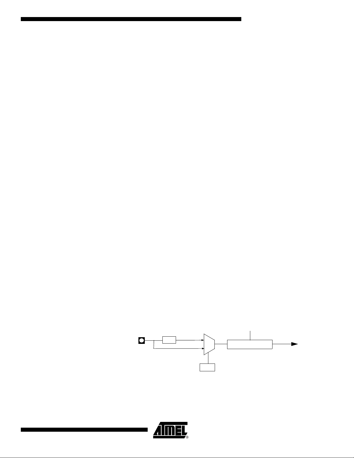
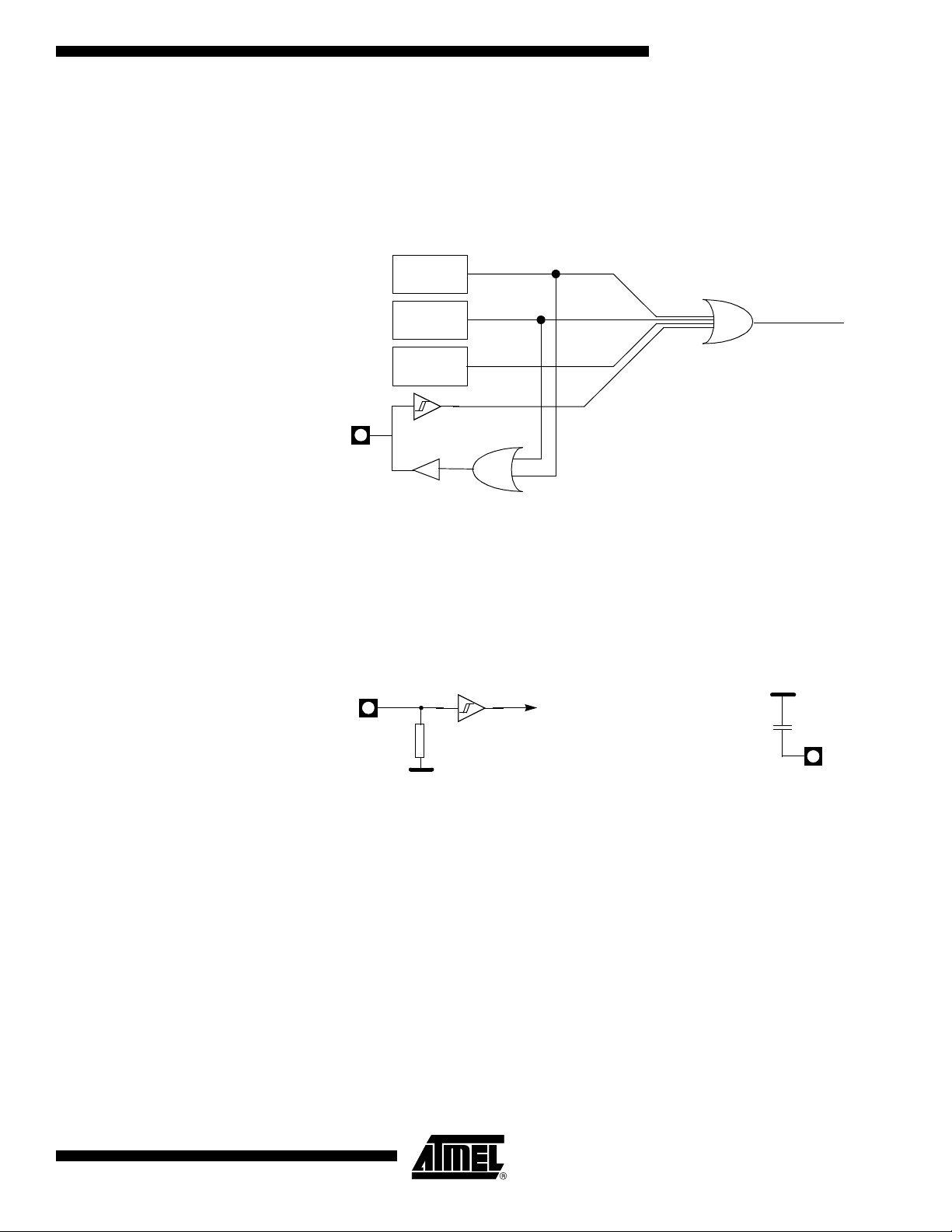
Port Types
2 CPU
Input
Pin
Strong
Medium
N
Weak
P
Clock Delay
Port Latch
Data
Data
DPU
AUXR.7
P P
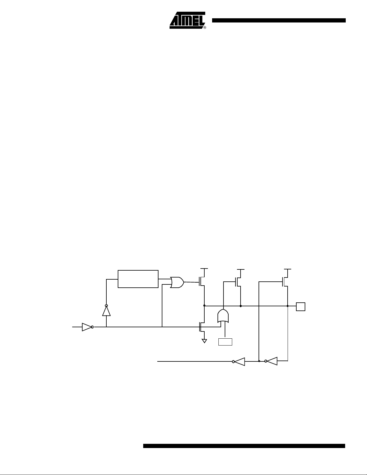
AT89C51RD2/ED2 I/O ports (P1, P2, P3, P4, P5) implement the quasi-bidirectional output that is common on the 80C51 and most of its derivatives. This output type can be
used as both an input and output without the need to reconfigure the port. This is possible because when the port outputs a logic high, it is weakly driven, allowing an external
device to pull the pin low. When the pin is pulled low, it is driven strongly and able to sink
a fairly large current. These features are somewhat similar to an open drain output
except that there are three pull-up transistors in the quasi-bidirectional output that serve
different purposes. One of these pull-ups, called the "weak" pull-up, is turned on whenever the port latch for the pin contains a logic 1. The weak pull-up sources a very small
current that will pull the pin high if it is left floating. A second pull-up, called the "medium"
pull-up, is turned on when the port latch for the pin contains a logic 1 and the pin itself is
also at a logic 1 level. This pull-up provides the primary source current for a quasi-bidirectional pin that is outputting a 1. If a pin that has a logic 1 on it is pulled low by an
external device, the medium pull-up turns off, and only the weak pull-up remains on. In
order to pull the pin low under these conditions, the external device has to sink enough
current to overpower the medium pull-up and take the voltage on the port pin below its
input threshold.
The third pull-up is referred to as the "strong" pull-up. This pull-up is used to speed up
low-to-high transitions on a quasi-bidirectional port pin when the port latch changes from
a logic 0 to a logic 1. When this occurs, the strong pull-up turns on for a brief time, two
CPU clocks, in order to pull the port pin high quickly. Then it turns off again.
The DPU bit (bit 7 in AUXR register) allows to disable the permanent weak pull up of all
ports when latch data is logical 0.
The quasi-bidirectional port configuration is shown in Figure 3.
Figure 3. Quasi-Bidirectional Output
14
4235I–8051–04/07
Page 15
AT89C51RD2/ED2
Oscillator
Registers
To optimize the power consumption and execution time needed for a specific task, an
internal prescaler feature has been implemented between the oscillator and the CPU
and peripherals.
Table 14. CKRL Register
CKRL – Clock Reload Register (97h)
7 6 5 4 3 2 1 0
CKRL7 CKRL6 CKRL5 CKRL4 CKRL3 CKRL2 CKRL1 CKRL0
Bit Number Mnemonic Description
7:0 CKRL
Clock Reload Register
Prescaler value
Reset Value = 1111 1111b
Not bit addressable
Table 15. PCON Register
PCON – Power Control Register (87h)
7 6 5 4 3 2 1 0
SMOD1 SMOD0 - POF GF1 GF0 PD IDL
Bit Number Bit Mnemonic Description
7 SMOD1
6 SMOD0
5 -
4 POF
3 GF1
2 GF0
1 PD
0 IDL
Serial Port Mode bit 1
Set to select double baud rate in mode 1, 2 or 3.
Serial Port Mode bit 0
Cleared to select SM0 bit in SCON register.
Set to select FE bit in SCON register.
Reserved
The value read from this bit is indeterminate. Do not set this bit.
Power-off Flag
Cleared by software to recognize the next reset type.
Set by hardware when VCC rises from 0 to its nominal voltage. Can
also be set by software.
General-purpose Flag
Cleared by software for general-purpose usage.
Set by software for general-purpose usage.
General-purpose Flag
Cleared by software for general-purpose usage.
Set by software for general-purpose usage.
Power-down Mode bit
Cleared by hardware when reset occurs.
Set to enter power-down mode.
Idle Mode bit
Cleared by hardware when interrupt or reset occurs.
Set to enter idle mode.
4235I–8051–04/07
Reset Value = 00X1 0000b Not bit addressable
15
Page 16
AT89C51RD2/ED2
Functional Block Diagram
Xtal2
Xtal1
Osc
CLK
Idle
CPU Clock
CKRL
Reload
8-bit
Prescaler-Divider
Reset
Peripheral Clock
:2
X2
0
1
F
OSC
CKCON0
CLK
Periph
CPU
CKRL = 0xFF?
0
1
F
CP U
F
=
CL K P ERI P H
F
OS C
2 255 CKR L–( )×
-----------------------------------------------=
F
CP U
F
=
CL K P ERI P H
F
OS C
4 255 CKR L–( )×
-----------------------------------------------=
Figure 4. Functional Oscillator Block Diagram
Prescaler Divider • A hardware RESET puts the prescaler divider in the following state:
• CKRL = FFh: F
CLK CPU
• Any value between FFh down to 00h can be written by software into CKRL register
in order to divide frequency of the selected oscillator:
• CKRL = 00h: minimum frequency
F
CLK CPU
F
CLK CPU
= F
CLK PERIPH
= F
CLK PERIPH
• CKRL = FFh: maximum frequency
F
CLK CPU
F
CLK CPU
F
CLK CPU
and F
= F
CLK PERIPH
= F
CLK PERIPH
CLK PERIPH
= F
= F
= F
= F
= F
= F
CLK PERIPH
/1020 (Standard Mode)
OSC
/510 (X2 Mode)
OSC
/2 (Standard Mode)
OSC
(X2 Mode)
OSC
/2 (Standard C51 feature)
OSC
16
In X2 Mode, for CKRL<>0xFF:
In X1 Mode, for CKRL<>0xFF then:
4235I–8051–04/07
Page 17
AT89C51RD2/ED2
XTAL1
2
CKCON0
X2
8-bit Prescaler
F
OSC
FXTAL
0
1
XTAL1:2
F
CLK CPU
F
CLK PERIPH
CKRL
Enhanced Features
X2 Feature
In comparison to the original 80C52, the AT89C51RD2/ED2 implements some new features, which are
:
• X2 option
• Dual Data Pointer
• Extended RAM
• Programmable Counter Array (PCA)
• Hardware Watchdog
• SPI interface
• 4-level interrupt priority system
• Power-off flag
• ONCE mode
• ALE disabling
• Some enhanced features are also located in the UART and the Timer 2
The AT89C51RD2/ED2 core needs only 6 clock periods per machine cycle. This feature
called ‘X2’ provides the following advantages:
• Divide frequency crystals by 2 (cheaper crystals) while keeping same CPU power.
• Save power consumption while keeping same CPU power (oscillator power saving).
• Save power consumption by dividing dynamically the operating frequency by 2 in
operating and idle modes.
• Increase CPU power by 2 while keeping same crystal frequency.
In order to keep the original C51 compatibility, a divider by 2 is inserted between the
XTAL1 signal and the main clock input of the core (phase generator). This divider may
be disabled by software.
Description The clock for the whole circuit and peripherals is first divided by two before being used
by the CPU core and the peripherals.
This allows any cyclic ratio to be accepted on XTAL1 input. In X2 mode, as this divider is
bypassed, the signals on XTAL1 must have a cyclic ratio between 40 to 60%.
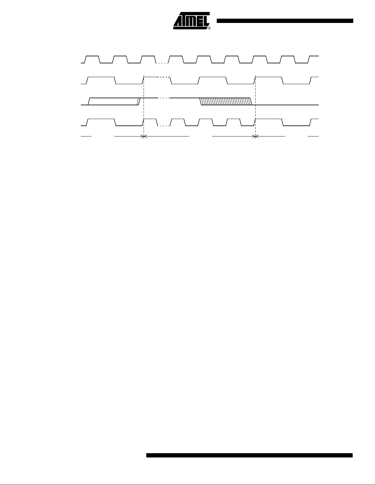
Figure 5 shows the clock generation block diagram. X2 bit is validated on the rising edge
of the XTAL1 ÷ 2 to avoid glitches when switching from X2 to STD mode. Figure 6
shows the switching mode waveforms.
Figure 5. Clock Generation Diagram
4235I–8051–04/07
17
Page 18
AT89C51RD2/ED2
Figure 6. Mode Switching Waveforms
XTAL1:2
XTAL1
CPU Clock
X2 Bit
X2 ModeSTD Mode STD Mode
F
OSC
The X2 bit in the CKCON0 register (see Table 16) allows a switch from 12 clock periods
per instruction to 6 clock periods and vice versa. At reset, the speed is set according to
X2 bit of Hardware Security Byte (HSB). By default, Standard mode is active. Setting the
X2 bit activates the X2 feature (X2 mode).
The T0X2, T1X2, T2X2, UartX2, PcaX2, and WdX2 bits in the CKCON0 register (Table
16) and SPIX2 bit in the CKCON1 register (see Table 17) allows a switch from standard
peripheral speed (12 clock periods per peripheral clock cycle) to fast peripheral speed (6
clock periods per peripheral clock cycle). These bits are active only in X2 mode.
18
4235I–8051–04/07
Page 19

AT89C51RD2/ED2
Table 16. CKCON0 Register
CKCON0 - Clock Control Register (8Fh)
7 6 5 4 3 2 1 0
- WDX2 PCAX2 SIX2 T2X2 T1X2 T0X2 X2
Bit
Number
7 Reserved The values for this bit are indeterminite. Do not set this bit.
6 WDX2
5 PCAX2
4 SIX2
3 T2X2
Bit
Mnemonic Description
Watchdog Clock
(This control bit is validated when the CPU clock X2 is set; when X2 is low, this bit
has no effect).
Cleared to select 6 clock periods per peripheral clock cycle.
Set to select 12 clock periods per peripheral clock cycle.
Programmable Counter Array Clock
(This control bit is validated when the CPU clock X2 is set; when X2 is low, this bit
has no effect).
Cleared to select 6 clock periods per peripheral clock cycle. Set to select 12 clock
periods per peripheral clock cycle.
Enhanced UART Clock (Mode 0 and 2)
(This control bit is validated when the CPU clock X2 is set; when X2 is low, this bit
has no effect).
Cleared to select 6 clock periods per peripheral clock cycle. Set to select 12 clock
periods per peripheral clock cycle.
Timer2 Clock
(This control bit is validated when the CPU clock X2 is set; when X2 is low, this bit
has no effect).
Cleared to select 6 clock periods per peripheral clock cycle.
Set to select 12 clock periods per peripheral clock cycle.
Timer1 Clock
2 T1X2
1 T0X2
0 X2
(This control bit is validated when the CPU clock X2 is set; when X2 is low, this bit
has no effect).
Cleared to select 6 clock periods per peripheral clock cycle. Set to select 12 clock
periods per peripheral clock cycle.
Timer0 Clock
(This control bit is validated when the CPU clock X2 is set; when X2 is low, this bit
has no effect).
Cleared to select 6 clock periods per peripheral clock cycle. Set to select 12 clock
periods per peripheral clock cycle.
CPU Clock
Cleared to select 12 clock periods per machine cycle (STD mode) for CPU and
all the peripherals. Set to select 6 clock periods per machine cycle (X2 mode)
and to enable the individual peripherals’X2’ bits. Programmed by hardware after
Power-up regarding Hardware Security Byte (HSB), Default setting, X2 is
cleared.
Reset Value = 0000 000’HSB. X2’b (See “Hardware Security Byte”)
Not bit addressable
4235I–8051–04/07
19
Page 20

AT89C51RD2/ED2
Table 17. CKCON1 Register
CKCON1 - Clock Control Register (AFh)
7 6 5 4 3 2 1 0
- - - - - - - SPIX2
Bit
Number
7 - Reserved
6 - Reserved
5 - Reserved
4 - Reserved
3 - Reserved
2 - Reserved
1 - Reserved
0 SPIX2
Bit
Mnemonic Description
SPI (This control bit is validated when the CPU clock X2 is set; when X2 is low,
this bit has no effect).
Clear to select 6 clock periods per peripheral clock cycle.
Set to select 12 clock periods per peripheral clock cycle.
Reset Value = XXXX XXX0b
Not bit addressable
20
4235I–8051–04/07
Page 21
AT89C51RD2/ED2
External Data Memory
AUXR1(A2H)
DPS
DPH(83H) DPL(82H)
07
DPTR0
DPTR1
Dual Data Pointer Register (DPTR)
Figure 7. Use of Dual Pointer
The additional data pointer can be used to speed up code execution and reduce code
size.
The dual DPTR structure is a way by which the chip will specify the address of an external data memory location. There are two 16-bit DPTR registers that address the external
memory, and a single bit called DPS = AUXR1.0 (see Table 18) that allows the program
code to switch between them (Refer to Figure 7).
4235I–8051–04/07
21
Page 22

AT89C51RD2/ED2
Table 18. AUXR1 Register
AUXR1- Auxiliary Register 1(0A2h)
7 6 5 4 3 2 1 0
- - ENBOOT - GF3 0 - DPS
Bit
Number
7 -
6 -
5 ENBOOT
4 -
3 GF3 This bit is a general-purpose user flag.
2 0 Always cleared
1 -
0 DPS
Bit
Mnemonic Description
Reserved
The value read from this bit is indeterminate. Do not set this bit.
Reserved
The value read from this bit is indeterminate. Do not set this bit.
Enable Boot Flash
Cleared to disable boot ROM.
Set to map the boot ROM between F800h - 0FFFFh.
Reserved
The value read from this bit is indeterminate. Do not set this bit.
(1)
Reserved
The value read from this bit is indeterminate. Do not set this bit.
Data Pointer Selection
Cleared to select DPTR0.
Set to select DPTR1.
Reset Value = XXXX XX0X0b
Not bit addressable
Note: 1. Bit 2 stuck at 0; this allows to use INC AUXR1 to toggle DPS without changing GF3.
22
ASSEMBLY LANGUAGE
; Block move using dual data pointers
; Modifies DPTR0, DPTR1, A and PSW
; note: DPS exits opposite of entry state
; unless an extra INC AUXR1 is added
;
00A2 AUXR1 EQU 0A2H
;
0000 909000MOV DPTR,#SOURCE ; address of SOURCE
0003 05A2 INC AUXR1 ; switch data pointers
0005 90A000 MOV DPTR,#DEST ; address of DEST
0008 LOOP:
0008 05A2 INC AUXR1 ; switch data pointers
000A E0 MOVX A,@DPTR ; get a byte from SOURCE
000B A3 INC DPTR ; increment SOURCE address
000C 05A2 INC AUXR1 ; switch data pointers
000E F0 MOVX @DPTR,A ; write the byte to DEST
000F A3 INC DPTR ; increment DEST address
0010 70F6JNZ LOOP ; check for 0 terminator
0012 05A2 INC AUXR1 ; (optional) restore DPS
4235I–8051–04/07
Page 23

AT89C51RD2/ED2
INC is a short (2 bytes) and fast (12 clocks) way to manipulate the DPS bit in the AUXR1
SFR. However, note that the INC instruction does not directly force the DPS bit to a particular state, but simply toggles it. In simple routines, such as the block move example,
only the fact that DPS is toggled in the proper sequence matters, not its actual value. In
other words, the block move routine works the same whether DPS is '0' or '1' on entry.
Observe that without the last instruction (INC AUXR1), the routine will exit with DPS in
the opposite state.
4235I–8051–04/07
23
Page 24

AT89C51RD2/ED2
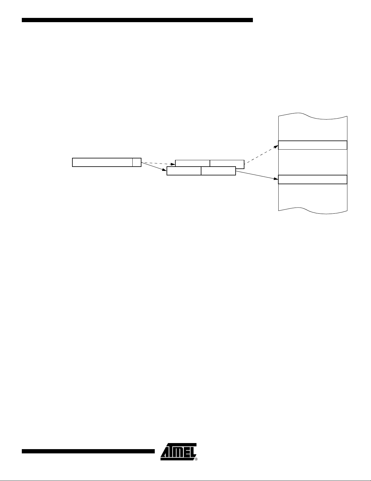
Expanded RAM
XRAM
Upper
128 Bytes
Internal
RAM
Lower
128 Bytes
Internal
RAM
Special
Function
Register
80h 80h
00
0FFh or 6FFh
0FFh
00
0FFh
External
Data
Memory
0000
00FFh up to 06FFh
0FFFFh
Indirect Accesses
Direct Accesses
Direct or Indirect
Accesses
7Fh
(XRAM)
The AT89C51RD2/ED2 provides additional on-chip random access memory (RAM)
space for increased data parameter handling and high level language usage.
AT89C51RD2/ED2 device haS expanded RAM in external data space configurable up
to 1792 bytes (see Table 19).
The AT89C51RD2/ED2 internal data memory is mapped into four separate segments.
The four segments are:
1. The Lower 128 bytes of RAM (addresses 00h to 7Fh) are directly and indirectly
addressable.
2. The Upper 128 bytes of RAM (addresses 80h to FFh) are indirectly addressable
only.
3. The Special Function Registers, SFRs, (addresses 80h to FFh) are directly
addressable only.
4. The expanded RAM bytes are indirectly accessed by MOVX instructions, and
with the EXTRAM bit cleared in the AUXR register (see Table 19).
The lower 128 bytes can be accessed by either direct or indirect addressing. The Upper
128 bytes can be accessed by indirect addressing only. The Upper 128 bytes occupy
the same address space as the SFR. That means they have the same address, but are
physically separate from SFR space.
Figure 8. Internal and External Data Memory Address
24
When an instruction accesses an internal location above address 7Fh, the CPU knows
whether the access is to the upper 128 bytes of data RAM or to SFR space by the
addressing mode used in the instruction.
• Instructions that use direct addressing access SFR space. For example: MOV
0A0H, # data, accesses the SFR at location 0A0h (which is P2).
• Instructions that use indirect addressing access the Upper 128 bytes of data RAM.
For example: MOV @R0, # data where R0 contains 0A0h, accesses the data byte
at address 0A0h, rather than P2 (whose address is 0A0h).
• The XRAM bytes can be accessed by indirect addressing, with EXTRAM bit cleared
and MOVX instructions. This part of memory which is physically located on-chip,
logically occupies the first bytes of external data memory. The bits XRS0 and XRS1
are used to hide a part of the available XRAM as explained in Table 19. This can be
4235I–8051–04/07
Page 25

AT89C51RD2/ED2
useful if external peripherals are mapped at addresses already used by the internal
XRAM.
• With EXTRAM = 0, the XRAM is indirectly addressed, using the MOVX instruction in
combination with any of the registers R0, R1 of the selected bank or DPTR. An
access to XRAM will not affect ports P0, P2, P3.6 (WR) and P3.7 (RD). For
example, with EXTRAM = 0, MOVX @R0, # data where R0 contains 0A0H,
accesses the XRAM at address 0A0H rather than external memory. An access to
external data memory locations higher than the accessible size of the XRAM will be
performed with the MOVX DPTR instructions in the same way as in the standard
80C51, with P0 and P2 as data/address busses, and P3.6 and P3.7 as write and
read timing signals. Accesses to XRAM above 0FFH can only be done by the use of
DPTR.
• With EXTRAM = 1, MOVX @Ri and MOVX @DPTR will be similar to the standard
80C51.MOVX @ Ri will provide an eight-bit address multiplexed with data on Port0
and any output port pins can be used to output higher order address bits. This is to
provide the external paging capability. MOVX @DPTR will generate a sixteen-bit
address. Port2 outputs the high-order eight address bits (the contents of DPH) while
Port0 multiplexes the low-order eight address bits (DPL) with data. MOVX @ Ri and
MOVX @DPTR will generate either read or write signals on P3.6 (WR) and P3.7
(RD).
The stack pointer (SP) may be located anywhere in the 256 bytes RAM (lower and
upper RAM) internal data memory. The stack may not be located in the XRAM.
The M0 bit allows to stretch the XRAM timings; if M0 is set, the read and write pulses
are extended from 6 to 30 clock periods. This is useful to access external slow
peripherals.
4235I–8051–04/07
25
Page 26
AT89C51RD2/ED2
Registers
Table 19. AUXR Register
AUXR - Auxiliary Register (8Eh)
7 6 5 4 3 2 1 0
DPU - M0 XRS2 XRS1 XRS0 EXTRAM AO
Bit
Number
7 DPU
6 -
5 M0
4 XRS2 XRAM Size
3 XRS1
2 XRS0
1 EXTRAM
Bit
Mnemonic Description
Disable Weak Pull-up
Cleared by software to activate the permanent weak pull-up (default)
Set by software to disable the weak pull-up (reduce power consumption)
Reserved
The value read from this bit is indeterminate. Do not set this bit.
Pulse length
Cleared to stretch MOVX control: the RD and the WR pulse length is 6 clock
periods (default).
Set to stretch MOVX control: the RD and the WR pulse length is 30 clock periods.
XRS2 XRS1 XRS0 XRAM size
0 0 0 256 bytes
0 0 1 512 bytes
0 1 0 768 bytes(default)
0 1 1 1024 bytes
1 0 0 1792 bytes
EXTRAM bit
Cleared to access internal XRAM using movx @ Ri/ @ DPTR.
Set to access external memory.
Programmed by hardware after Power-up regarding Hardware Security Byte
(HSB), default setting, XRAM selected.
26
ALE Output bit
0 AO
Cleared, ALE is emitted at a constant rate of 1/6 the oscillator frequency (or 1/3 if
X2 mode is used). (default) Set, ALE is active only during a MOVX or MOVC
instruction is used.
Reset Value = 0X00 10’HSB. XRAM’0b
Not bit addressable
4235I–8051–04/07
Page 27
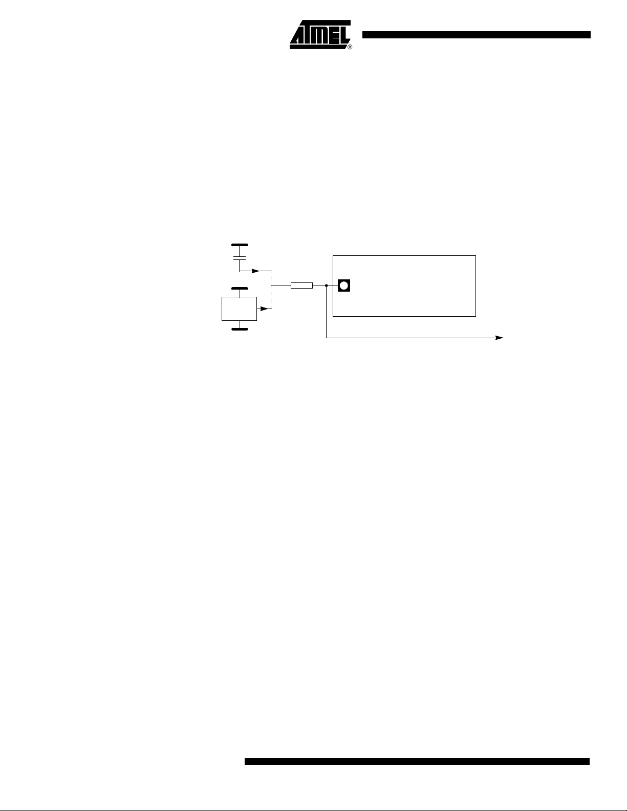
Reset
Power
Monitor
Hardware
Watchdog
PCA
Watchdog
RST
Internal Reset
RST
R
RST
VSS
To internal reset
RST
VDD
+
b. Power-on Reseta. RST input circuitry
AT89C51RD2/ED2
Introduction
Reset Input
The reset sources are: Power Management, Hardware Watchdog, PCA Watchdog and
Reset input.
Figure 9. Reset schematic
The Reset input can be used to force a reset pulse longer than the internal reset controlled by the Power Monitor. RST input has a pull-down resistor allowing power-on
reset by simply connecting an external capacitor to VCC as shown in Figure 10. Resistor
value and input characteristics are discussed in the Section “DC Characteristics” of the
AT89C51RD2/ED2 datasheet.
4235I–8051–04/07
Figure 10. Reset Circuitry and Power-On Reset
27
Page 28
AT89C51RD2/ED2
Reset Output
RST
VDD
+
VSS
VDD
RST
1K
To other
on-board
circuitry
AT89C51XD2
Reset output can be generated by two sources:
• Internal POR/PFD
• Hardware watchdog timer
As detailed in Section “Hardware Watchdog Timer”, page 86, the WDT generates a 96clock period pulse on the RST pin.
In order to properly propagate this pulse to the rest of the application in case of external
capacitor or power-supply supervisor circuit, a 1 kΩ resistor must be added as shown
Figure 11.
Figure 11. Recommended Reset Output Schematic
28
4235I–8051–04/07
Page 29
AT89C51RD2/ED2
VCC
Power On Reset
Power Fail Detect
Voltage Regulator
XTAL1
(1)
CPU core
Memories
Peripherals
Regulated
Supply
RST pin
Hardware
Watchdog
PCA
Watchdog
Internal Reset
Power Monitor
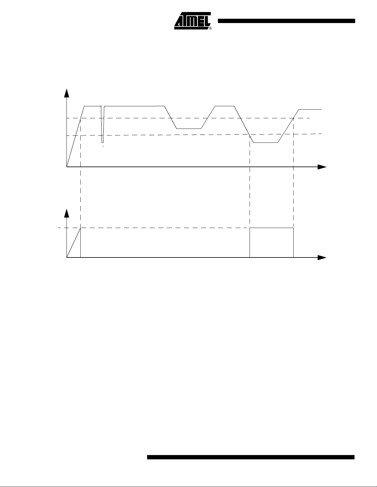
Description
The POR/PFD function monitors the internal power-supply of the CPU core memories
and the peripherals, and if needed, suspends their activity when the internal power supply falls below a safety threshold. This is achieved by applying an internal reset to them.
By g e neratin g the Rese t the Power Moni t o r i n s ures a co r r ect s t art u p w h e n
AT89C51RD2/ED2 is powered up.
In order to startup and maintain the microcontroller in correct operating mode, VCC has
to be stabilized in the VCC operating range and the oscillator has to be stabilized with a
nominal amplitude compatible with logic level VIH/VIL.
These parameters are controlled during the three phases: power-up, normal operation
and power going down. See Figure 12.
Figure 12. Power Monitor Block Diagram
4235I–8051–04/07
Note: 1. Once XTAL1 High and low levels reach above and below VIH/VIL. a 1024 clock
period delay will extend the reset coming from the Power Fail Detect. If the power
falls below the Power Fail Detect threshold level, the Reset will be applied
immediately.
The Voltage regulator generates a regulated internal supply for the CPU core the memories and the peripherals. Spikes on the external Vcc are smoothed by the voltage
regulator.
29
Page 30
AT89C51RD2/ED2
Figure 13. Power Fail Detect
Vcc
t
Reset
Vcc
VPFDP
VPFDM
The Power fail detect monitor the supply generated by the voltage regulator and generate a reset if this supply falls below a safety threshold as illustrated in the Figure 13
below.
When the power is applied, the Power Monitor immediately asserts a reset. Once the
internal supply after the voltage regulator reach a safety level, the power monitor then
looks at the XTAL clock input. The internal reset will remain asserted until the Xtal1 levels are above and below VIH and VIL. Further more. An internal counter will count 1024
clock periods before the reset is de-asserted.
If the internal power supply falls below a safety level, a reset is immediately asserted.
.
30
4235I–8051–04/07
Page 31

AT89C51RD2/ED2
Timer 2
Auto-reload Mode
The Timer 2 in the AT89C51RD2/ED2 is the standard C52 Timer 2. It is a 16-bit
timer/counter: the count is maintained by two eight-bit timer registers, TH2 and TL2 are
cascaded. It is controlled by T2CON (Table 20) and T2MOD (Table 21) registers. Timer
2 operation is similar to Timer 0 and Timer 1. C/T2 selects F
external pin T2 (counter operation) as the timer clock input. Setting TR2 allows TL2 to
increment by the selected input.
Timer 2 has 3 operating modes: capture, autoreload and Baud Rate Generator. These
modes are selected by the combination of RCLK, TCLK and CP/RL2 (T2CON).
Refer to the Atmel 8-bit Microcontroller Hardware Manual for the description of Capture
and Baud Rate Generator Modes.
Timer 2 includes the following enhancements:
• Auto-reload mode with up or down counter
• Programmable clock-output
The auto-reload mode configures Timer 2 as a 16-bit timer or event counter with automatic reload. If DCEN bit in T2MOD is cleared, Timer 2 behaves as in 80C52 (refer to
the Atmel C51 Microcontroller Hardware Manual). If DCEN bit is set, Timer 2 acts as an
Up/down timer/counter as shown in Figure 14. In this mode the T2EX pin controls the
direction of count.
When T2EX is high, Timer 2 counts up. Timer overflow occurs at FFFFh which sets the
TF2 flag and generates an interrupt request. The overflow also causes the 16-bit value
in RCAP2H and RCAP2L registers to be loaded into the timer registers TH2 and TL2.
/12 (timer operation) or
OSC
When T2EX is low, Timer 2 counts down. Timer underflow occurs when the count in the
timer registers TH2 and TL2 equals the value stored in RCAP2H and RCAP2L registers.
The underflow sets TF2 flag and reloads FFFFh into the timer registers.
The EXF2 bit toggles when Timer 2 overflows or underflows according to the direction of
the count. EXF2 does not generate any interrupt. This bit can be used to provide 17-bit
resolution.
4235I–8051–04/07
31
Page 32

AT89C51RD2/ED2
Figure 14. Auto-reload Mode Up/Down Counter (DCEN = 1)
(DOWN COUNTING RELOAD VALUE)
C/T2
TF2
TR2
T2
EXF2
TH2
(8-bit)
TL2
(8-bit)
RCAP2H
(8-bit)
RCAP2L
(8-bit)
FFh
(8-bit)
FFh
(8-bit)
TOGGLE
(UP COUNTING RELOAD VALUE)
TIMER 2
INTERRUPT
F
CLK PERIPH
0
1
T2CON
T2CON
T2CON
T2CON
T2EX:
If DCEN = 1, 1 = UP
If DCEN = 1, 0 = DOWN
If DCEN = 0, up counting
:
6
Clock O– utFrequ e ncy
F
CL K P E R I P H
4 65536 RCAP2H RCA P2L⁄ )–(×
---------------------------------------------------------------------------------------------
=
Programmable Clock-output
In the clock-out mode, Timer 2 operates as a 50% duty-cycle, programmable clock generator (See Figure 15). The input clock increments TL2 at frequency F
timer repeatedly counts to overflow from a loaded value. At overflow, the contents of
RCAP2H and RCAP2L registers are loaded into TH2 and TL2. In this mode, Timer 2
overflows do not generate interrupts. The formula gives the clock-out frequency as a
function of the system oscillator frequency and the value in the RCAP2H and RCAP2L
registers:
For a 16 MHz system clock, Timer 2 has a programmable frequency range of 61 Hz
(F
T2 pin (P1.0).
Timer 2 is programmed for the clock-out mode as follows:
• Set T2OE bit in T2MOD register.
• Clear C/T2 bit in T2CON register.
CLK PERIPH
• Determine the 16-bit reload value from the formula and enter it in RCAP2H/RCAP2L
registers.
• Enter a 16-bit initial value in timer registers TH2/TL2. It can be the same as the
reload value or a different one depending on the application.
• To start the timer, set TR2 run control bit in T2CON register.
It is possible to use Timer 2 as a baud rate generator and a clock generator simultane o u s l y. Fo r this configurat io n, th e baud rates and clock f re quencies are no t
independent since both functions use the values in the RCAP2H and RCAP2L registers.
16
/2
)
to 4 MHz (F
CLK PERIPH
CLK PERIPH
/4). The generated clock signal is brought out to
/2. The
32
4235I–8051–04/07
Page 33

Figure 15. Clock-out Mode C/T2 = 0
:6
EXF2
TR2
OVERFLOW
T2EX
TH
2
(8-bit)
TL2
(8-bit)
TIMER 2
RCAP2H
(8-bit)
RCAP2L
(8-bit)
T2OE
T2
FCLK PERIPH
T2CON
T2CON
T2CON
T2MOD
INTERRUPT
Q D
Toggle
EXEN2
AT89C51RD2/ED2
4235I–8051–04/07
33
Page 34

AT89C51RD2/ED2
Registers
Table 20. T2CON Register
T2CON - Timer 2 Control Register (C8h)
7 6 5 4 3 2 1 0
TF2 EXF2 RCLK TCLK EXEN2 TR2 C/T2# CP/RL2#
Bit
Number
7 TF2
6 EXF2
5 RCLK
4 TCLK
3 EXEN2
2 TR2
Bit
Mnemonic Description
Timer 2 overflow Flag
Must be cleared by software.
Set by hardware on Timer 2 overflow, if RCLK = 0 and TCLK = 0.
Timer 2 External Flag
Set when a capture or a reload is caused by a negative transition on T2EX pin if
EXEN2 = 1.
When set, causes the CPU to vector to Timer 2 interrupt routine when Timer 2
interrupt is enabled.
Must be cleared by software. EXF2 doesn’t cause an interrupt in Up/down
counter mode (DCEN = 1).
Receive Clock bit
Cleared to use timer 1 overflow as receive clock for serial port in mode 1 or 3.
Set to use Timer 2 overflow as receive clock for serial port in mode 1 or 3.
Transmit Clock bit
Cleared to use timer 1 overflow as transmit clock for serial port in mode 1 or 3.
Set to use Timer 2 overflow as transmit clock for serial port in mode 1 or 3.
Timer 2 External Enable bit
Cleared to ignore events on T2EX pin for Timer 2 operation.
Set to cause a capture or reload when a negative transition on T2EX pin is
detected, if Timer 2 is not used to clock the serial port.
Timer 2 Run control bit
Cleared to turn off Timer 2.
Set to turn on Timer 2.
34
Timer/Counter 2 select bit
1 C/T2#
0 CP/RL2#
Cleared for timer operation (input from internal clock system: F
Set for counter operation (input from T2 input pin, falling edge trigger). Must be 0
for clock out mode.
Timer 2 Capture/Reload bit
If RCLK = 1 or TCLK = 1, CP/RL2# is ignored and timer is forced to auto-reload
on Timer 2 overflow.
Cleared to auto-reload on Timer 2 overflows or negative transitions on T2EX pin
if EXEN2=1.
Set to capture on negative transitions on T2EX pin if EXEN2 = 1.
Reset Value = 0000 0000b
Bit addressable
CLK PERIPH
).
4235I–8051–04/07
Page 35

AT89C51RD2/ED2
Table 21. T2MOD Register
T2MOD - Timer 2 Mode Control Register (C9h)
7 6 5 4 3 2 1 0
- - - - - - T2OE DCEN
Bit
Number
7 -
6 -
5 -
4 -
3 -
2 -
1 T2OE
0 DCEN
Bit
Mnemonic Description
Reserved
The value read from this bit is indeterminate. Do not set this bit.
Reserved
The value read from this bit is indeterminate. Do not set this bit.
Reserved
The value read from this bit is indeterminate. Do not set this bit.
Reserved
The value read from this bit is indeterminate. Do not set this bit.
Reserved
The value read from this bit is indeterminate. Do not set this bit.
Reserved
The value read from this bit is indeterminate. Do not set this bit.
Timer 2 Output Enable bit
Cleared to program P1.0/T2 as clock input or I/O port.
Set to program P1.0/T2 as clock output.
Down Counter Enable bit
Cleared to disable Timer 2 as up/down counter.
Set to enable Timer 2 as up/down counter.
Reset Value = XXXX XX00b
Not bit addressable
4235I–8051–04/07
35
Page 36

AT89C51RD2/ED2
Programmable Counter Array (PCA)
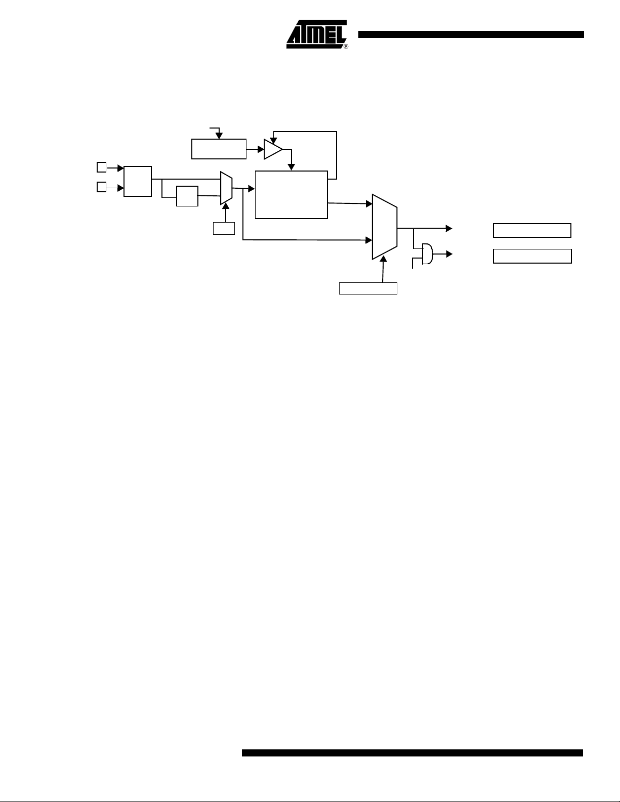
The PCA provides more timing capabilities with less CPU intervention than the standard
timer/counters. Its advantages include reduced software overhead and improved accuracy. The PCA consists of a dedicated timer/counter which serves as the time base for
an array of five compare/capture modules. Its clock input can be programmed to count
any one of the following signals:
• Peripheral clock frequency (F
• Peripheral clock frequency (F
CLK PERIPH
CLK PERIPH
) ÷ 6
) ÷ 2
• Timer 0 overflow
• External input on ECI (P1.2)
Each compare/capture module can be programmed in any one of the following modes:
• Rising and/or falling edge capture
• Software timer
• High-speed output
• Pulse width modulator
Module 4 can also be programmed as a watchdog timer (see Section "PCA Watchdog
Timer", page 47).
When the compare/capture modules are programmed in the capture mode, software
timer, or high speed output mode, an interrupt can be generated when the module executes its function. All five modules plus the PCA timer overflow share one interrupt
vector.
The PCA timer/counter and compare/capture modules share Port 1 for external I/O.
These pins are listed below. If one or several bits in the port are not used for the PCA,
they can still be used for standard I/O.
PCA Component External I/O Pin
16-bit Counter P1.2/ECI
16-bit Module 0 P1.3/CEX0
16-bit Module 1 P1.4/CEX1
16-bit Module 2 P1.5/CEX2
16-bit Module 3 P1.6/CEX3
The PCA timer is a common time base for all five modules (see Figure 16). The timer
count source is determined from the CPS1 and CPS0 bits in the CMOD register
(Table 22) and can be programmed to run at:
• 1/6 the
• 1/2 the
peripheral clock frequency (F
peripheral clock frequency (F
CLK PERIPH
CLK PERIPH
)
)
• The Timer 0 overflow
• The input on the ECI pin (P1.2)
36
4235I–8051–04/07
Page 37

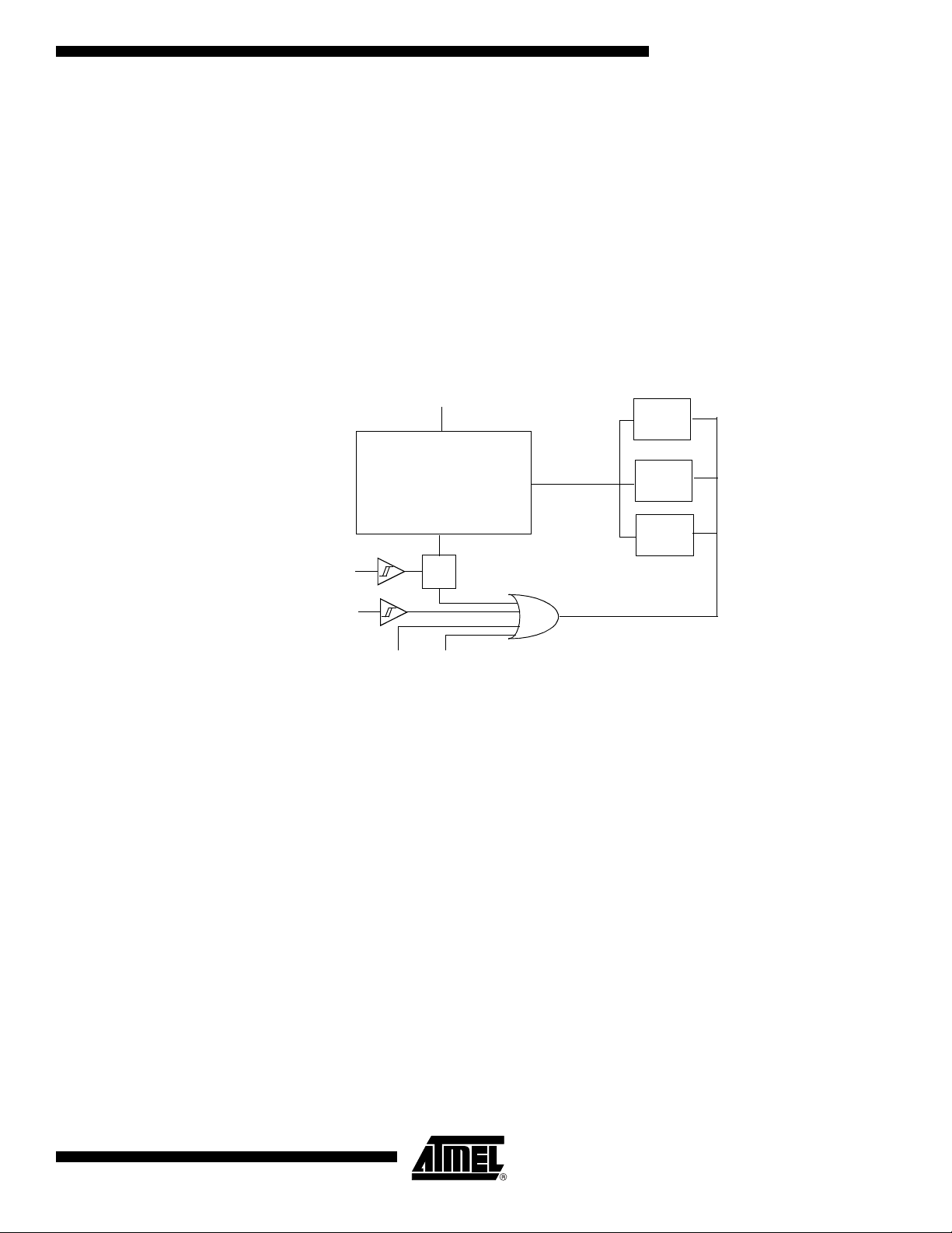
Figure 16. PCA Timer/Counter
CIDL CPS1 CPS0 ECF
IT
CH CL
16 Bit Up Counter
To PCA
Modules
F
CLK PERIPH
/6
F
CLK PERIPH
/2
T0 OVF
P1.2
Idle
CMOD
0xD9
WDTE
CF CR
CCON
0xD8
CCF4 CCF3 CCF2 CCF1 CCF0
Overflow
AT89C51RD2/ED2
The CMOD register includes three additional bits associated with the PCA (See
Figure 16 and Table 22).
• The CIDL bit which allows the PCA to stop during idle mode.
• The WDTE bit which enables or disables the watchdog function on module 4.
• The ECF bit which when set causes an interrupt and the PCA overflow flag CF (in
the CCON SFR) to be set when the PCA timer overflows.
4235I–8051–04/07
37
Page 38

AT89C51RD2/ED2
Table 22. CMOD Register
CMOD - PCA Counter Mode Register (D9h)
7 6 5 4 3 2 1 0
CIDL WDTE - - - CPS1 CPS0 ECF
Bit
Number
7 CIDL
6 WDTE
5 -
4 -
3 -
2 CPS1 PCA Count Pulse Select
1 CPS0
0 ECF
Bit
Mnemonic Description
Counter Idle Control
Cleared to program the PCA Counter to continue functioning during idle Mode.
Set to program PCA to be gated off during idle.
Watchdog Timer Enable
Cleared to disable Watchdog Timer function on PCA Module 4.
Set to enable Watchdog Timer function on PCA Module 4.
Reserved
The value read from this bit is indeterminate. Do not set this bit.
Reserved
The value read from this bit is indeterminate. Do not set this bit.
Reserved
The value read from this bit is indeterminate. Do not set this bit.
CPS1 CPS0 Selected PCA input
0 0 Internal clock F
0 1 Internal clock F
1 0 Timer 0 Overflow
1 1 External clock at ECI/P1.2 pin (max rate = F
PCA Enable Counter Overflow Interrupt
Cleared to disable CF bit in CCON to inhibit an interrupt.
Set to enable CF bit in CCON to generate an interrupt.
CLK PERIPH
CLK PERIPH
/6
/2
CLK PERIPH
/4)
38
Reset Value = 00XX X000b
Not bit addressable
The CCON register contains the run control bit for the PCA and the flags for the PCA
timer (CF) and each module (Refer to Table 23).
• Bit CR (CCON.6) must be set by software to run the PCA. The PCA is shut off by
clearing this bit.
• Bit CF: The CF bit (CCON.7) is set when the PCA counter overflows and an
interrupt will be generated if the ECF bit in the CMOD register is set. The CF bit can
only be cleared by software.
• Bits 0 through 4 are the flags for the modules (bit 0 for module 0, bit 1 for module 1,
etc.) and are set by hardware when either a match or a capture occurs. These flags
also can only be cleared by software.
4235I–8051–04/07
Page 39

AT89C51RD2/ED2
Table 23. CCON Register
CCON - PCA Counter Control Register (D8h)
7 6 5 4 3 2 1 0
CF CR - CCF4 CCF3 CCF2 CCF1 CCF0
Bit
Number
7 CF
6 CR
5 -
4 CCF4
3 CCF3
2 CCF2
1 CCF1
Bit
Mnemonic Description
PCA Counter Overflow flag
Set by hardware when the counter rolls over. CF flags an interrupt if bit ECF in
CMOD is set. CF
may be set by either hardware or software but can only be cleared by software.
PCA Counter Run control bit
Must be cleared by software to turn the PCA counter off.
Set by software to turn the PCA counter on.
Reserved
The value read from this bit is indeterminate. Do not set this bit.
PCA Module 4 interrupt flag
Must be cleared by software.
Set by hardware when a match or capture occurs.
PCA Module 3 interrupt flag
Must be cleared by software.
Set by hardware when a match or capture occurs.
PCA Module 2 interrupt flag
Must be cleared by software.
Set by hardware when a match or capture occurs.
PCA Module 1 interrupt flag
Must be cleared by software.
Set by hardware when a match or capture occurs.
4235I–8051–04/07
PCA Module 0 interrupt flag
0 CCF0
Must be cleared by software.
Set by hardware when a match or capture occurs.
Reset Value = 00X0 0000b
Bit addressable
The watchdog timer function is implemented in Module 4 (See Figure 19).
The PCA interrupt system is shown in Figure 17.
39
Page 40

AT89C51RD2/ED2
Figure 17. PCA Interrupt System
CF CR
CCON
0xD8
CCF4 CCF3 CCF2 CCF1 CCF0
Module 4
Module 3
Module 2
Module 1
Module 0
ECF
PCA Timer/Counter
ECCFn
CCAPMn.0CMOD.0
IEN0.6 IEN0.7
To Interrupt
Priority Decoder
EC EA
PCA Modules: each one of the five compare/capture modules has six possible functions. It can perform:
• 16-bit Capture, positive-edge triggered
• 16-bit Capture, negative-edge triggered
• 16-bit Capture, both positive and negative-edge triggered
• 16-bit Software Timer
• 16-bit High Speed Output
• 8-bit Pulse Width Modulator
In addition, Module 4 can be used as a Watchdog Timer.
Each module in the PCA has a special function register associated with it. These registers are: CCAPM0 for Module 0, CCAPM1 for Module 1, etc. (See Table 24). The
registers contain the bits that control the mode that each module will operate in.
• The ECCF bit (CCAPMn.0 where n = 0, 1, 2, 3, or 4 depending on the module)
enables the CCF flag in the CCON SFR to generate an interrupt when a match or
compare occurs in the associated module.
• PWM (CCAPMn.1) enables the pulse width modulation mode.
• The TOG bit (CCAPMn.2) when set causes the CEX output associated with the
module to toggle when there is a match between the PCA counter and the modules
capture/compare register.
• The match bit MAT (CCAPMn.3) when set will cause the CCFn bit in the CCON
register to be set when there is a match between the PCA counter and the modules
capture/compare register.
• The next two bits CAPN (CCAPMn.4) and CAPP (CCAPMn.5) determine the edge
that a capture input will be active on. The CAPN bit enables the negative edge, and
the CAPP bit enables the positive edge. If both bits are set both edges will be
enabled and a capture will occur for either transition.
• The last bit in the register ECOM (CCAPMn.6) when set enables the comparator
function.
40
4235I–8051–04/07
Page 41

AT89C51RD2/ED2
Table 24 shows the CCAPMn settings for the various PCA functions.
Table 24. CCAPMn Registers (n = 0-4)
CCAPM0 - PCA Module 0 Compare/Capture Control Register (0DAh)
CCAPM1 - PCA Module 1 Compare/Capture Control Register (0DBh)
CCAPM2 - PCA Module 2 Compare/Capture Control Register (0DCh)
CCAPM3 - PCA Module 3 Compare/Capture Control Register (0DDh)
CCAPM4 - PCA Module 4 Compare/Capture Control Register (0DEh)
7 6 5 4 3 2 1 0
- ECOMn CAPPn CAPNn MATn TOGn PWMn ECCFn
Bit
Number
7 -
6 ECOMn
5 CAPPn
4 CAPNn
3 MATn
2 TOGn
1 PWMn
Bit
Mnemonic Description
Reserved
The value read from this bit is indeterminate. Do not set this bit.
Enable Comparator
Cleared to disable the comparator function.
Set to enable the comparator function.
Capture Positive
Cleared to disable positive edge capture.
Set to enable positive edge capture.
Capture Negative
Cleared to disable negative edge capture.
Set to enable negative edge capture.
Match
When MATn = 1, a match of the PCA counter with this module's
compare/capture register causes the CCFn bit in CCON to be set, flagging an
interrupt.
Toggle
When TOGn = 1, a match of the PCA counter with this module's
compare/capture register causes the CEXn pin to toggle.
Pulse Width Modulation Mode
Cleared to disable the CEXn pin to be used as a pulse width modulated output.
Set to enable the CEXn pin to be used as a pulse width modulated output.
4235I–8051–04/07
Enable CCF interrupt
0 CCF0
Cleared to disable compare/capture flag CCFn in the CCON register to generate
an interrupt.
Set to enable compare/capture flag CCFn in the CCON register to generate an
interrupt.
Reset Value = X000 0000b
Not bit addressable
41
Page 42

AT89C51RD2/ED2
Table 25. PCA Module Modes (CCAPMn Registers)
ECOMn CAPPn CAPNn MATn TOGn PWMm ECCFn Module Function
0 0 0 0 0 0 0 No Operation
X 1 0 0 0 0 X
X 0 1 0 0 0 X
X 1 1 0 0 0 X
1 0 0 1 0 0 X
1 0 0 1 1 0 X 16-bit High Speed Output
1 0 0 0 0 1 0 8-bit PWM
1 0 0 1 X 0 X Watchdog Timer (module 4 only)
16-bit capture by a positive-edge
trigger on CEXn
16-bit capture by a negative trigger
on CEXn
16-bit capture by a transition on
CEXn
16-bit Software Timer/Compare
mode.
There are two additional registers associated with each of the PCA modules. They are
CCAPnH and CCAPnL and these are the registers that store the 16-bit count when a
capture occurs or a compare should occur. When a module is used in the PWM mode
these registers are used to control the duty cycle of the output (See Table 26 &
Table 27).
Table 26. CCAPnH Registers (n = 0 - 4)
CCAP0H - PCA Module 0 Compare/Capture Control Register High (0FAh)
CCAP1H - PCA Module 1 Compare/Capture Control Register High (0FBh)
CCAP2H - PCA Module 2 Compare/Capture Control Register High (0FCh)
CCAP3H - PCA Module 3 Compare/Capture Control Register High (0FDh)
CCAP4H - PCA Module 4 Compare/Capture Control Register High (0FEh)
7 6 5 4 3 2 1 0
- - - - - - - -
Bit
Number
7 - 0 -
Bit
Mnemonic Description
PCA Module n Compare/Capture Control
CCAPnH Value
Reset Value = 0000 0000b
Not bit addressable
42
4235I–8051–04/07
Page 43

AT89C51RD2/ED2
Table 27. CCAPnL Registers (n = 0 - 4)
CCAP0L - PCA Module 0 Compare/Capture Control Register Low (0EAh)
CCAP1L - PCA Module 1 Compare/Capture Control Register Low (0EBh)
CCAP2L - PCA Module 2 Compare/Capture Control Register Low (0ECh)
CCAP3L - PCA Module 3 Compare/Capture Control Register Low (0EDh)
CCAP4L - PCA Module 4 Compare/Capture Control Register Low (0EEh)
7 6 5 4 3 2 1 0
- - - - - - - -
Bit
Number
7 - 0 -
Bit
Mnemonic Description
PCA Module n Compare/Capture Control
CCAPnL Value
Reset Value = 0000 0000b
Not bit addressable
Table 28. CH Register
CH - PCA Counter Register High (0F9h)
7 6 5 4 3 2 1 0
- - - - - - - -
Bit
Number
7 - 0 -
Bit
Mnemonic Description
PCA counter
CH Value
Reset Value = 0000 0000b
Not bit addressable
Table 29. CL Register
4235I–8051–04/07
CL - PCA Counter Register Low (0E9h)
7 6 5 4 3 2 1 0
- - - - - - - -
Bit
Number
7 - 0 -
Bit
Mnemonic Description
PCA Counter
CL Value
Reset Value = 0000 0000b
Not bit addressable
43
Page 44

AT89C51RD2/ED2
PCA Capture Mode
CF CR
CCON
0xD8
CH CL
CCAPnH CCAPnL
CCF4 CCF3 CCF2 CCF1 CCF0
PCA IT
PCA Counter/Timer
ECOMn
CCAPMn, n= 0 to 4
0xDA to 0xDE
CAPNn MATn TOGn PWMn ECCFnCAPPn
Cex.n
Capture
Figure 18. PCA Capture Mode
To use one of the PCA modules in the capture mode either one or both of the CCAPM
bits CAPN and CAPP for that module must be set. The external CEX input for the module (on port 1) is sampled for a transition. When a valid transition occurs the PCA
hardware loads the value of the PCA counter registers (CH and CL) into the module's
capture registers (CCAPnL and CCAPnH). If the CCFn bit for the module in the CCON
SFR and the ECCFn bit in the CCAPMn SFR are set then an interrupt will be generated
(Refer to Figure 18).
16-bit Software Timer/ Compare Mode
44
The PCA modules can be used as software timers by setting both the ECOM and MAT
bits in the modules CCAPMn register. The PCA timer will be compared to the module's
capture registers and when a match occurs an interrupt will occur if the CCFn (CCON
SFR) and the ECCFn (CCAPMn SFR) bits for the module are both set (See Figure 19).
4235I–8051–04/07
Page 45

Figure 19. PCA Compare Mode and PCA Watchdog Timer
CH CL
CCAPnH CCAPnL
ECOMn
CCAPMn, n = 0 to 4
0xDA to 0xDE
CAPNn MA Tn TOGn PWMn ECCFnCA PPn
16 bit comparator
Match
CCON
0xD8
PCA IT
Enable
PCA counter/timer
RESET *
CIDL CPS1 CPS0 E CF
CMOD
0xD9
WDTE
Reset
Write to
CCAPnL
Write to
CCAPnH
CF CCF2 CCF1 CCF0
CR
CCF3CCF4
1 0
AT89C51RD2/ED2
High Speed Output Mode
Before enabling ECOM bit, CCAPnL and CCAPnH should be set with a non zero value,
otherwise an unwanted match could happen. Writing to CCAPnH will set the ECOM bit.
Once ECOM is set, writing CCAPnL will clear ECOM so that an unwanted match doesn’t
occur while modifying the compare value. Writing to CCAPnH will set ECOM. For this
reason, user software should write CCAPnL first, and then CCAPnH. Of course, the
ECOM bit can still be controlled by accessing to CCAPMn register.
In this mode the CEX output (on port 1) associated with the PCA module will toggle
each time a match occurs between the PCA counter and the modules capture registers.
To activate this mode the TOG, MAT, and ECOM bits in the module's CCAPMn SFR
must be set (See Figure 20).
A prior write must be done to CCAPnL and CCAPnH before writing the ECOMn bit.
4235I–8051–04/07
45
Page 46

AT89C51RD2/ED2
Figure 20. PCA High Speed Output Mode
CH CL
CCAPnH CCAPnL
ECOMn
CCAPMn, n = 0 to 4
0xDA to 0xDE
CAPNn MATn TOGn P WMn ECCFnCAPPn
16 bit comparator
Match
CF CR
CCON
0xD8
CCF4 CCF3 CCF2 CCF1 CCF0
PCA IT
Enable
CEXn
PCA counter/timer
Write to
CCAPnH
Reset
Writ e to
CCAPnL
1
0
Before enabling ECOM bit, CCAPnL and CCAPnH should be set with a non zero value,
otherwise an unwanted match could happen.
Once ECOM is set, writing CCAPnL will clear ECOM so that an unwanted match doesn’t
occur while modifying the compare value. Writing to CCAPnH will set ECOM. For this
reason, user software should write CCAPnL first, and then CCAPnH. Of course, the
ECOM bit can still be controlled by accessing to CCAPMn register.
Pulse Width Modulator Mode
All of the PCA modules can be used as PWM outputs. Figure 21 shows the PWM function. The frequency of the output depends on the source for the PCA timer. All of the
modules will have the same frequency of output because they all share the PCA timer.
The duty cycle of each module is independently variable using the modules capture register CCAPLn. When the value of the PCA CL SFR is less than the value in the modules
CCAPLn SFR the output will be low, when it is equal to or greater than the output will be
high. When CL overflows from FF to 00, CCAPLn is reloaded with the value in CCAPHn.
This allows updating the PWM without glitches. The PWM and ECOM bits in the module's CCAPMn register must be set to enable the PWM mode.
46
4235I–8051–04/07
Page 47

Figure 21. PCA PWM Mode
CL
CCAPnH
CCAPnL
ECOMn
CCAPMn, n= 0 to 4
0xDA to 0xDE
CAPNn MATn TOGn PWMn ECCFnCAPPn
8-bit Comparator
CEXn
“0”
“1”
Enable
PCA Counter/Timer
Overflow
AT89C51RD2/ED2
PCA Watchdog Timer
An on-board watchdog timer is available with the PCA to improve the reliability of the
system without increasing chip count. Watchdog timers are useful for systems that are
susceptible to noise, power glitches, or electrostatic discharge. Module 4 is the only
PCA module that can be programmed as a watchdog. However, this module can still be
used for other modes if the watchdog is not needed. Figure 19 shows a diagram of how
the watchdog works. The user pre-loads a 16-bit value in the compare registers. Just
like the other compare modes, this 16-bit value is compared to the PCA timer value. If a
match is allowed to occur, an internal reset will be generated. This will not cause the
RST pin to be driven high.
In order to hold off the reset, the user has three options:
1. Periodically change the compare value so it will never match the PCA timer.
2. Periodically change the PCA timer value so it will never match the compare
values.
3. Disable the watchdog by clearing the WDTE bit before a match occurs and then
re-enable it.
4235I–8051–04/07
47
Page 48

AT89C51RD2/ED2
The first two options are more reliable because the watchdog timer is never disabled as
in option #3. If the program counter ever goes astray, a match will eventually occur and
cause an internal reset. The second option is also not recommended if other PCA modules are being used. Remember, the PCA timer is the time base for all modules;
changing the time base for other modules would not be a good idea. Thus, in most applications the first solution is the best option.
This watchdog timer won’t generate a reset out on the reset pin.
48
4235I–8051–04/07
Page 49

AT89C51RD2/ED2
RITIRB8TB8RENSM2SM1SM0/FE
IDLPDGF0GF1POF-SMOD0SMOD1
To UART framing error control
SM0 to UART mode control (SMOD0 = 0)
Set FE bit if stop bit is 0 (framing error) (SMOD0 = 1)
SCON (98h)
PCON (87h)
Data byte
RI
SMOD0=X
Stop
bit
Start
bit
RXD
D7D6D5D4D3D2D1D0
FE
SMOD0=1
Serial I/O Port
Framing Error Detection
The serial I/O port in the AT89C51RD2/ED2 is compatible with the serial I/O port in the
80C52.
It provides both synchronous and asynchronous communication modes. It operates as a
Universal Asynchronous Receiver and Transmitter (UART) in three full-duplex modes
(Modes 1, 2 and 3). Asynchronous transmission and reception can occur simultaneously
and at different baud rates
Serial I/O port includes the following enhancements:
• Framing error detection
• Automatic address recognition
Framing bit error detection is provided for the three asynchronous modes (modes 1, 2
and 3). To enable the framing bit error detection feature, set SMOD0 bit in PCON register (See Figure 22).
Figure 22. Framing Error Block Diagram
When this feature is enabled, the receiver checks each incoming data frame for a valid
stop bit. An invalid stop bit may result from noise on the serial lines or from simultaneous
transmission by two CPUs. If a valid stop bit is not found, the Framing Error bit (FE) in
SCON register (See Table 33.) bit is set.
Software may examine FE bit after each reception to check for data errors. Once set,
only software or a reset can clear FE bit. Subsequently received frames with valid stop
bits cannot clear FE bit. When FE feature is enabled, RI rises on stop bit instead of the
last data bit (See Figure 23. and Figure 24.).
Figure 23. UART Timings in Mode 1
4235I–8051–04/07
49
Page 50

AT89C51RD2/ED2
Figure 24. UART Timings in Modes 2 and 3
RI
SMOD0=0
Data byte Ninth
bit
Stop
bit
Start
bit
RXD
D8D7D6D5D4D3D2D1D0
RI
SMOD0=1
FE
SMOD0=1
Automatic Address Recognition
The automatic address recognition feature is enabled when the multiprocessor communication feature is enabled (SM2 bit in SCON register is set).
Implemented in hardware, automatic address recognition enhances the multiprocessor
communication feature by allowing the serial port to examine the address of each
incoming command frame. Only when the serial port recognizes its own address, the
receiver sets RI bit in SCON register to generate an interrupt. This ensures that the CPU
is not interrupted by command frames addressed to other devices.
If desired, the user may enable the automatic address recognition feature in mode 1.In
this configuration, the stop bit takes the place of the ninth data bit. Bit RI is set only when
the received command frame address matches the device’s address and is terminated
by a valid stop bit.
To support automatic address recognition, a device is identified by a given address and
a broadcast address.
Note: The multiprocessor communication and automatic address recognition features cannot
be enabled in mode 0 (i. e. setting SM2 bit in SCON register in mode 0 has no effect).
Given Address Each device has an individual address that is specified in SADDR register; the SADEN
register is a mask byte that contains don’t-care bits (defined by zeros) to form the
device’s given address. The don’t-care bits provide the flexibility to address one or more
slaves at a time. The following example illustrates how a given address is formed.
To address a device by its individual address, the SADEN mask byte must be 1111
1111b.
For example:
SADDR0101 0110b
SADEN1111 1100b
Given0101 01XXb
50
The following is an example of how to use given addresses to address different slaves:
Slave A:SADDR1111 0001b
SADEN1111 1010b
Given1111 0X0Xb
Slave B:SADDR1111 0011b
SADEN1111 1001b
Given1111 0XX1b
Slave C:SADDR1111 0010b
SADEN1111 1101b
Given1111 00X1b
4235I–8051–04/07
Page 51

AT89C51RD2/ED2
The SADEN byte is selected so that each slave may be addressed separately.
For slave A, bit 0 (the LSB) is a don’t-care bit; for slaves B and C, bit 0 is a 1.To communicate with slave A only, the master must send an address where bit 0 is clear (e. g.
1111 0000b).
For slave A, bit 1 is a 1; for slaves B and C, bit 1 is a don’t care bit. To communicate with
slaves B and C, but not slave A, the master must send an address with bits 0 and 1 both
set (e. g. 1111 0011b).
To communicate with slaves A, B and C, the master must send an address with bit 0 set,
bit 1 clear, and bit 2 clear (e. g. 1111 0001b).
Broadcast Address A broadcast address is formed from the logical OR of the SADDR and SADEN registers
with zeros defined as don’t-care bits, e. g. :
SADDR 0101 0110b
SADEN 1111 1100b
Broadcast =SADDR OR SADEN1111 111Xb
The use of don’t-care bits provides flexibility in defining the broadcast address, however
in most applications, a broadcast address is FFh. The following is an example of using
broadcast addresses:
Slave A:SADDR1111 0001b
SADEN1111 1010b
Broadcast1111 1X11b,
Slave B:SADDR1111 0011b
SADEN1111 1001b
Broadcast1111 1X11B,
Slave C:SADDR=1111 0011b
SADEN1111 1101b
Broadcast1111 1111b
For slaves A and B, bit 2 is a don’t care bit; for slave C, bit 2 is set. To communicate with
all of the slaves, the master must send an address FFh. To communicate with slaves A
and B, but not slave C, the master can send and address FBh.
Reset Addresses On reset, the SADDR and SADEN registers are initialized to 00h, i. e. the given and
broadcast addresses are XXXX XXXXb (all don’t-care bits). This ensures that the serial
port will reply to any address, and so, that it is backwards compatible with the 80C51
microcontrollers that do not support automatic address recognition.
4235I–8051–04/07
51
Page 52

AT89C51RD2/ED2
Registers
RCLK
/ 16
RBCK
INT_BRG
0
1
TIMER1
0
1
0
1
TIMER2
INT_BRG
TIMER1
TIMER2
TIMER_BRG_RX
Rx Clock
/ 16
0
1
TIMER_BRG_TX
Tx Clock
TBCK
TCLK
Table 30. SADEN Register
SADEN - Slave Address Mask Register (B9h)
7 6 5 4 3 2 1 0
Reset Value = 0000 0000b
Not bit addressable
Table 31. SADDR Register
SADDR - Slave Address Register (A9h)
7 6 5 4 3 2 1 0
Reset Value = 0000 0000b
Not bit addressable
Baud Rate Selection for UART for Mode 1 and 3
The Baud Rate Generator for transmit and receive clocks can be selected separately via
the T2CON and BDRCON registers.
Figure 25. Baud Rate Selection
52
4235I–8051–04/07
Page 53

Table 32. Baud Rate Selection Table UART
0
1
Overflow
SPD
BDRCON.1
BRG
(8 bits)
BRL
(8 bits)
F
Clk Periph
÷ 6
BRR
BDRCON.4
0
1
SMOD1
PCON.7
÷ 2
INT_BRG
Baud_Rate =
6
(1-SPD)
⋅ 32 ⋅ (256 -BRL)
2
SMOD1
⋅ F
PER
BRL = 256 -
6
(1-SPD)
⋅ 32 ⋅ Baud_Rate
2
SMOD1
⋅ F
PER
AT89C51RD2/ED2
Internal Baud Rate Generator
(BRG)
Figure 26. Internal Baud Rate
TCLK
(T2CON)
0 0 0 0 Timer 1 Timer 1
1 0 0 0 Timer 2 Timer 1
0 1 0 0 Timer 1 Timer 2
1 1 0 0 Timer 2 Timer 2
X 0 1 0 INT_BRG Timer 1
X 1 1 0 INT_BRG Timer 2
0 X 0 1 Timer 1 INT_BRG
1 X 0 1 Timer 2 INT_BRG
X X 1 1 INT_BRG INT_BRG
RCLK
(T2CON)
TBCK
(BDRCON)
RBCK
(BDRCON)
Clock Source
UART Tx
Clock Source
UART Rx
When the internal Baud Rate Generator is used, the Baud Rates are determined by the
BRG overflow depending on the BRL reload value, the value of SPD bit (Speed Mode)
in BDRCON register and the value of the SMOD1 bit in PCON register.
4235I–8051–04/07
• The baud rate for UART is token by formula:
53
Page 54

AT89C51RD2/ED2
Table 33. SCON Register
SCON - Serial Control Register (98h)
7 6 5 4 3 2 1 0
FE/SM0 SM1 SM2 REN TB8 RB8 TI RI
Bit
Number
7
6 SM1
5 SM2
4 REN
3 TB8
Bit
Mnemonic Description
Framing Error bit (SMOD0=1)
FE
SM0
Clear to reset the error state, not cleared by a valid stop bit.
Set by hardware when an invalid stop bit is detected.
SMOD0 must be set to enable access to the FE bit.
Serial port Mode bit 0
Refer to SM1 for serial port mode selection.
SMOD0 must be cleared to enable access to the SM0 bit.
Serial port Mode bit 1
SM0 SM1 Mode Baud Rate
0 0 Shift Register F
0 1 8-bit UART Variable
1 0 9-bit UART F
1 1 9-bit UART Variable
Serial port Mode 2 bit / Multiprocessor Communication Enable bit
Clear to disable multiprocessor communication feature.
Set to enable multiprocessor communication feature in mode 2 and 3, and
eventually mode 1.This bit should be cleared in mode 0.
Reception Enable bit
Clear to disable serial reception.
Set to enable serial reception.
Transmitter Bit 8 / Ninth bit to transmit in modes 2 and 3
Clear to transmit a logic 0 in the 9th bit.
Set to transmit a logic 1 in the 9th bit.
XTAL
XTAL
/12 (or F
/64 or F
/6 in mode X2)
XTAL
/32
XTAL
54
2 RB8
1 TI
0 RI
Reset Value = 0000 0000b
Bit addressable
Receiver Bit 8 / Ninth bit received in modes 2 and 3
Cleared by hardware if 9th bit received is a logic 0.
Set by hardware if 9th bit received is a logic 1.
In mode 1, if SM2 = 0, RB8 is the received stop bit. In mode 0 RB8 is not
used.
Transmit Interrupt flag
Clear to acknowledge interrupt.
Set by hardware at the end of the 8th bit time in mode 0 or at the beginning
of the stop bit in the other modes.
Receive Interrupt flag
Clear to acknowledge interrupt.
Set by hardware at the end of the 8th bit time in mode 0, see Figure 23.
and Figure 24. in the other modes.
4235I–8051–04/07
Page 55

AT89C51RD2/ED2
Table 34. Example of Computed Value When X2=1, SMOD1=1, SPD=1
Baud Rates F
115200 247 1.23 243 0.16
57600 238 1.23 230 0.16
38400 229 1.23 217 0.16
28800 220 1.23 204 0.16
19200 203 0.63 178 0.16
9600 149 0.31 100 0.16
4800 43 1.23 - -
= 16. 384 MHz F
OSC
BRL Error (%) BRL Error (%)
= 24MHz
OSC
Table 35. Example of Computed Value When X2=0, SMOD1=0, SPD=0
Baud Rates F
4800 247 1.23 243 0.16
2400 238 1.23 230 0.16
1200 220 1.23 202 3.55
600 185 0.16 152 0.16
= 16. 384 MHz F
OSC
BRL Error (%) BRL Error (%)
= 24MHz
OSC
UART Registers
The baud rate generator can be used for mode 1 or 3 (refer to Figure 25.), but also for
mode 0 for UART, thanks to the bit SRC located in BDRCON register (Table 42.)
Table 36. SADEN Register
SADEN - Slave Address Mask Register for UART (B9h)
7 6 5 4 3 2 1 0
Reset Value = 0000 0000b
Table 37. SADDR Register
SADDR - Slave Address Register for UART (A9h)
7 6 5 4 3 2 1 0
Reset Value = 0000 0000b
4235I–8051–04/07
55
Page 56

AT89C51RD2/ED2
Table 38. SBUF Register
SBUF - Serial Buffer Register for UART (99h)
7 6 5 4 3 2 1 0
Reset Value = XXXX XXXXb
Table 39. BRL Register
BRL - Baud Rate Reload Register for the internal baud rate generator, UART (9Ah)
7 6 5 4 3 2 1 0
Reset Value = 0000 0000b
56
4235I–8051–04/07
Page 57

AT89C51RD2/ED2
Table 40. T2CON Register
T2CON - Timer 2 Control Register (C8h)
7 6 5 4 3 2 1 0
TF2 EXF2 RCLK TCLK EXEN2 TR2 C/T2# CP/RL2#
Bit
Number
7 TF2
6 EXF2
5 RCLK
4 TCLK
3 EXEN2
2 TR2
Bit
Mnemonic Description
Timer 2 overflow Flag
Must be cleared by software.
Set by hardware on timer 2 overflow, if RCLK = 0 and TCLK = 0.
Timer 2 External Flag
Set when a capture or a reload is caused by a negative transition on T2EX pin if
EXEN2=1.
When set, causes the CPU to vector to timer 2 interrupt routine when timer 2
interrupt is enabled.
Must be cleared by software. EXF2 doesn’t cause an interrupt in Up/down
counter mode (DCEN = 1)
Receive Clock bit for UART
Cleared to use timer 1 overflow as receive clock for serial port in mode 1 or 3.
Set to use timer 2 overflow as receive clock for serial port in mode 1 or 3.
Transmit Clock bit for UART
Cleared to use timer 1 overflow as transmit clock for serial port in mode 1 or 3.
Set to use timer 2 overflow as transmit clock for serial port in mode 1 or 3.
Timer 2 External Enable bit
Cleared to ignore events on T2EX pin for timer 2 operation.
Set to cause a capture or reload when a negative transition on T2EX pin is
detected, if timer 2 is not used to clock the serial port.
Timer 2 Run control bit
Cleared to turn off timer 2.
Set to turn on timer 2.
4235I–8051–04/07
Timer/Counter 2 select bit
1 C/T2#
0 CP/RL2#
Cleared for timer operation (input from internal clock system: F
Set for counter operation (input from T2 input pin, falling edge trigger). Must be
0 for clock out mode.
Timer 2 Capture/Reload bit
If RCLK=1 or TCLK=1, CP/RL2# is ignored and timer is forced to auto-reload on
timer 2 overflow.
Cleared to auto-reload on timer 2 overflows or negative transitions on T2EX pin
if EXEN2=1.
Set to capture on negative transitions on T2EX pin if EXEN2=1.
Reset Value = 0000 0000b
Bit addressable
CLK PERIPH
).
57
Page 58

AT89C51RD2/ED2
Table 41. PCON Register
PCON - Power Control Register (87h)
7 6 5 4 3 2 1 0
SMOD1 SMOD0 - POF GF1 GF0 PD IDL
Bit
Number
7 SMOD1
6 SMOD0
5 -
4 POF
3 GF1
2 GF0
1 PD
0 IDL
Bit
Mnemonic Description
Serial port Mode bit 1 for UART
Set to select double baud rate in mode 1, 2 or 3.
Serial port Mode bit 0 for UART
Cleared to select SM0 bit in SCON register.
Set to select FE bit in SCON register.
Reserved
The value read from this bit is indeterminate. Do not set this bit.
Power-Off Flag
Cleared to recognize next reset type.
Set by hardware when VCC rises from 0 to its nominal voltage. Can also be set
by software.
General purpose Flag
Cleared by user for general purpose usage.
Set by user for general purpose usage.
General purpose Flag
Cleared by user for general purpose usage.
Set by user for general purpose usage.
Power-Down mode bit
Cleared by hardware when reset occurs.
Set to enter power-down mode.
Idle mode bit
Cleared by hardware when interrupt or reset occurs.
Set to enter idle mode.
58
Reset Value = 00X1 0000b
Not bit addressable
Power-off flag reset value will be 1 only after a power on (cold reset). A warm reset
doesn’t affect the value of this bit.
4235I–8051–04/07
Page 59

AT89C51RD2/ED2
Table 42. BDRCON Register
BDRCON - Baud Rate Control Register (9Bh)
7 6 5 4 3 2 1 0
- - - BRR TBCK RBCK SPD SRC
Bit
Number
7 -
6 -
5 -
4 BRR
3 TBCK
2 RBCK
1 SPD
0 SRC
Bit
Mnemonic Description
Reserved
The value read from this bit is indeterminate. Do not set this bit
Reserved
The value read from this bit is indeterminate. Do not set this bit
Reserved
The value read from this bit is indeterminate. Do not set this bit.
Baud Rate Run Control bit
Cleared to stop the internal Baud Rate Generator.
Set to start the internal Baud Rate Generator.
Transmission Baud rate Generator Selection bit for UART
Cleared to select Timer 1 or Timer 2 for the Baud Rate Generator.
Set to select internal Baud Rate Generator.
Reception Baud Rate Generator Selection bit for UART
Cleared to select Timer 1 or Timer 2 for the Baud Rate Generator.
Set to select internal Baud Rate Generator.
Baud Rate Speed Control bit for UART
Cleared to select the SLOW Baud Rate Generator.
Set to select the FAST Baud Rate Generator.
Baud Rate Source select bit in Mode 0 for UART
Cleared to select F
mode).
Set to select the internal Baud Rate Generator for UARTs in mode 0.
/12 as the Baud Rate Generator (F
OSC
CLK PERIPH
/6 in X2
4235I–8051–04/07
Reset Value = XXX0 0000b
Not bit addressable
59
Page 60

AT89C51RD2/ED2
Keyboard Interface
P1:x
KBE.x
KBF.x
KBLS.x
0
1
Vcc
Internal Pullup
P1.0
Keyboard Interface
Interrupt Request
KBD
IE1
Input Circuitry
P1.1 Input Circuitry
P1.2 Input Circuitry
P1.3 Input Circuitry
P1.4 Input Circuitry
P1.5 Input Circuitry
P1.6 Input Circuitry
P1.7 Input Circuitry
KBDIT
The AT89C51RD2/ED2 implements a keyboard interface allowing the connection of a
8 x n matrix keyboard. It is based on 8 inputs with programmable interrupt capability on
both high or low level. These inputs are available as alternate function of P1 and allow to
exit from idle and power-down modes.
The keyboard interfaces with the C51 core through 3 special function registers: KBLS,
the Keyboard Level Selection register (Table 45), KBE, the Keyboard interrupt Enable
register (Table 44), and KBF, the Keyboard Flag register (Table 43).
Interrupt The keyboard inputs are considered as 8 independent interrupt sources sharing the
same interrupt vector. An interrupt enable bit (KBD in IE1) allows global enable or disable of the keyboard interrupt (see Figure 27). As detailed in Figure 28 each keyboard
input has the capability to detect a programmable level according to KBLS. x bit value.
Level detection is then reported in interrupt flags KBF.x that can be masked by software
using KBE. x bits.
This structure allow keyboard arrangement from 1 by n to 8 by n matrix and allows
usage of P1 inputs for other purpose.
Figure 27. Keyboard Interface Block Diagram
Power Reduction Mode P1 inputs allow exit from idle and power-down modes as detailed in Section “Power
60
Figure 28. Keyboard Input Circuitry
Management”, page 82.
4235I–8051–04/07
Page 61

AT89C51RD2/ED2
Registers
Table 43. KBF Register
KBF-Keyboard Flag Register (9Eh)
7 6 5 4 3 2 1 0
KBF7 KBF6 KBF5 KBF4 KBF3 KBF2 KBF1 KBF0
Bit
Number
7 KBF7
6 KBF6
5 KBF5
4 KBF4
Bit
Mnemonic Description
Keyboard line 7 flag
Set by hardware when the Port line 7 detects a programmed level. It generates a
Keyboard interrupt request if the KBKBIE.7 bit in KBIE register is set.
Must be cleared by software.
Keyboard line 6 flag
Set by hardware when the Port line 6 detects a programmed level. It generates a
Keyboard interrupt request if the KBIE.6 bit in KBIE register is set.
Must be cleared by software.
Keyboard line 5 flag
Set by hardware when the Port line 5 detects a programmed level. It generates a
Keyboard interrupt request if the KBIE.5 bit in KBIE register is set.
Must be cleared by software.
Keyboard line 4 flag
Set by hardware when the Port line 4 detects a programmed level. It generates a
Keyboard interrupt request if the KBIE.4 bit in KBIE register is set.
Must be cleared by software.
Keyboard line 3 flag
3 KBF3
2 KBF2
1 KBF1
0 KBF0
Set by hardware when the Port line 3 detects a programmed level. It generates a
Keyboard interrupt request if the KBIE.3 bit in KBIE register is set.
Must be cleared by software.
Keyboard line 2 flag
Set by hardware when the Port line 2 detects a programmed level. It generates a
Keyboard interrupt request if the KBIE.2 bit in KBIE register is set.
Must be cleared by software.
Keyboard line 1 flag
Set by hardware when the Port line 1 detects a programmed level. It generates a
Keyboard interrupt request if the KBIE.1 bit in KBIE register is set.
Must be cleared by software.
Keyboard line 0 flag
Set by hardware when the Port line 0 detects a programmed level. It generates a
Keyboard interrupt request if the KBIE.0 bit in KBIE register is set.
Must be cleared by software.
Reset Value = 0000 0000b
This register is read only access, all flags are automatically cleared by reading the
register.
4235I–8051–04/07
61
Page 62

AT89C51RD2/ED2
Table 44. KBE Register
KBE-Keyboard Input Enable Register (9Dh)
7 6 5 4 3 2 1 0
KBE7 KBE6 KBE5 KBE4 KBE3 KBE2 KBE1 KBE0
Bit
Number
7 KBE7
6 KBE6
5 KBE5
4 KBE4
3 KBE3
2 KBE2
1 KBE1
Bit
Mnemonic Description
Keyboard line 7 Enable bit
Cleared to enable standard I/O pin.
Set to enable KBF.7 bit in KBF register to generate an interrupt request.
Keyboard line 6 Enable bit
Cleared to enable standard I/O pin.
Set to enable KBF.6 bit in KBF register to generate an interrupt request.
Keyboard line 5 Enable bit
Cleared to enable standard I/O pin.
Set to enable KBF.5 bit in KBF register to generate an interrupt request.
Keyboard line 4 Enable bit
Cleared to enable standard I/O pin.
Set to enable KBF.4 bit in KBF register to generate an interrupt request.
Keyboard line 3 Enable bit
Cleared to enable standard I/O pin.
Set to enable KBF.3 bit in KBF register to generate an interrupt request.
Keyboard line 2 Enable bit
Cleared to enable standard I/O pin.
Set to enable KBF.2 bit in KBF register to generate an interrupt request.
Keyboard line 1 Enable bit
Cleared to enable standard I/O pin.
Set to enable KBF.1 bit in KBF register to generate an interrupt request.
0 KBE0
Keyboard line 0 Enable bit
Cleared to enable standard I/O pin.
Set to enable KBF.0 bit in KBF register to generate an interrupt request.
Reset Value = 0000 0000b
62
4235I–8051–04/07
Page 63

AT89C51RD2/ED2
Table 45. KBLS Register
KBLS-Keyboard Level Selector Register (9Ch)
7 6 5 4 3 2 1 0
KBLS7 KBLS6 KBLS5 KBLS4 KBLS3 KBLS2 KBLS1 KBLS0
Bit
Number
7 KBLS7
6 KBLS6
5 KBLS5
4 KBLS4
3 KBLS3
2 KBLS2
1 KBLS1
Bit
Mnemonic Description
Keyboard line 7 Level Selection bit
Cleared to enable a low level detection on Port line 7.
Set to enable a high level detection on Port line 7.
Keyboard line 6 Level Selection bit
Cleared to enable a low level detection on Port line 6.
Set to enable a high level detection on Port line 6.
Keyboard line 5 Level Selection bit
Cleared to enable a low level detection on Port line 5.
Set to enable a high level detection on Port line 5.
Keyboard line 4 Level Selection bit
Cleared to enable a low level detection on Port line 4.
Set to enable a high level detection on Port line 4.
Keyboard line 3 Level Selection bit
Cleared to enable a low level detection on Port line 3.
Set to enable a high level detection on Port line 3.
Keyboard line 2 Level Selection bit
Cleared to enable a low level detection on Port line 2.
Set to enable a high level detection on Port line 2.
Keyboard line 1 Level Selection bit
Cleared to enable a low level detection on Port line 1.
Set to enable a high level detection on Port line 1.
0 KBLS0
Keyboard line 0 Level Selection bit
Cleared to enable a low level detection on Port line 0.
Set to enable a high level detection on Port line 0.
Reset Value = 0000 0000b
4235I–8051–04/07
63
Page 64

AT89C51RD2/ED2
Serial Port Interface
Slave 1
MISO
MOSI
SCK
SS
MISO
MOSI
SCK
SS
PORT
0
1
2
3
Slave 3
MISO
MOSI
SCK
SS
Slave 4
MISO
MOSI
SCK
SS
Slave 2
MISO
MOSI
SCK
SS
VDD
Master
(SPI)
The Serial Peripheral Interface Module (SPI) allows full-duplex, synchronous, serial
communication between the MCU and peripheral devices, including other MCUs.
Features
Signal Description
Features of the SPI Module include the following:
• Full-duplex, three-wire synchronous transfers
• Master or Slave operation
• Eight programmable Master clock rates
• Serial clock with programmable polarity and phase
• Master Mode fault error flag with MCU interrupt capability
• Write collision flag protection
Figure 29 shows a typical SPI bus configuration using one Master controller and many
Slave peripherals. The bus is made of three wires connecting all the devices.
Figure 29. SPI Master/Slaves Interconnection
Master Output Slave Input
(MOSI)
Master Input Slave Output
(MISO)
SPI Serial Clock (SCK) This signal is used to synchronize the data movement both in and out of the devices
Slave Select (SS) Each Slave peripheral is selected by one Slave Select pin (SS). This signal must stay
64
The Master device selects the individual Slave devices by using four pins of a parallel
port to control the four SS pins of the Slave devices.
This 1-bit signal is directly connected between the Master Device and a Slave Device.
The MOSI line is used to transfer data in series from the Master to the Slave. Therefore,
it is an output signal from the Master, and an input signal to a Slave. A Byte (8-bit word)
is transmitted most significant bit (MSB) first, least significant bit (LSB) last.
This 1-bit signal is directly connected between the Slave Device and a Master Device.
The MISO line is used to transfer data in series from the Slave to the Master. Therefore,
it is an output signal from the Slave, and an input signal to the Master. A Byte (8-bit
word) is transmitted most significant bit (MSB) first, least significant bit (LSB) last.
through their MOSI and MISO lines. It is driven by the Master for eight clock cycles
which allows to exchange one Byte on the serial lines.
low for any message for a Slave. It is obvious that only one Master (SS high level) can
4235I–8051–04/07
Page 65

AT89C51RD2/ED2
drive the network. The Master may select each Slave device by software through port
pins (Figure 30). To prevent bus conflicts on the MISO line, only one slave should be
selected at a time by the Master for a transmission.
In a Master configuration, the SS line can be used in conjunction with the MODF flag in
the SPI Status register (SPSTA) to prevent multiple masters from driving MOSI and
SCK (see Error conditions).
A high level on the SS pin puts the MISO line of a Slave SPI in a high-impedance state.
The SS pin could be used as a general-purpose if the following conditions are met:
• The device is configured as a Master and the SSDIS control bit in SPCON is set.
This kind of configuration can be found when only one Master is driving the network
and there is no way that the SS pin could be pulled low. Therefore, the MODF flag in
the SPSTA will never be set
• The Device is configured as a Slave with CPHA and SSDIS control bits set
kind of configuration can happen when the system comprises one Master and one
Slave only. Therefore, the device should always be selected and there is no reason
that the Master uses the SS pin to select the communicating Slave device.
Note: 1. Clearing SSDIS control bit does not clear MODF.
2. Special care should be taken not to set SSDIS control bit when CPHA = ’0’ because
in this mode, the SS is used to start the transmission.
(1)
.
(2)
. This
Baud Rate In Master mode, the baud rate can be selected from a baud rate generator which is con-
trolled by three bits in the SPCON register: SPR2, SPR1 and SPR0.The Master clock is
selected from one of seven clock rates resulting from the division of the internal clock by
2, 4, 8, 16, 32, 64 or 128.
Table 46 gives the different clock rates selected by SPR2:SPR1:SPR0.
Table 46. SPI Master Baud Rate Selection
SPR2 SPR1 SPR0 Clock Rate Baud Rate Divisor (BD)
0 0 0 F
0 0 1 F
0 1 0 F
0 1 1 F
1 0 0 F
1 0 1 F
1 1 0 F
1 1 1 Don’t Use No BRG
CLK PERIPH
CLK PERIPH
CLK PERIPH
CLK PERIPH
CLK PERIPH
CLK PERIPH
CLK PERIPH
/2 2
/4 4
/8 8
/16 16
/32 32
/64 64
/128 128
4235I–8051–04/07
65
Page 66

AT89C51RD2/ED2
Functional Description
Shift Register
01
234567
Internal Bus
Pin
Control
Logic
MISO
MOSI
SCK
M
S
Clock
Logic
Clock
Divider
Clock
Select
/4
/64
/128
SPI Interrupt Request
8-bit bus
1-bit signal
SS
FCLK PERIPH
/32
/8
/16
Receive Data Register
SPDAT
SPI
Control
SPSTA
CPHA
SPR0
SPR1
CPOLMSTRSSDISSPEN
SPR2
SPCON
WCOL MODFSPIF
- - - - -
Figure 30 shows a detailed structure of the SPI Module.
Figure 30. SPI Module Block Diagram
Operating Modes The Serial Peripheral Interface can be configured in one of the two modes: Master mode
66
or Slave mode. The configuration and initialization of the SPI Module is made through
one register:
• The Serial Peripheral Control register (SPCON)
Once the SPI is configured, the data exchange is made using:
• SPCON
• The Serial Peripheral STAtus register (SPSTA)
• The Serial Peripheral DATa register (SPDAT)
During an SPI transmission, data is simultaneously transmitted (shifted out serially) and
received (shifted in serially). A serial clock line (SCK) synchronizes shifting and sampling on the two serial data lines (MOSI and MISO). A Slave Select line (SS) allows
individual selection of a Slave SPI device; Slave devices that are not selected do not
interfere with SPI bus activities.
When the Master device transmits data to the Slave device via the MOSI line, the Slave
device responds by sending data to the Master device via the MISO line. This implies
full-duplex transmission with both data out and data in synchronized with the same clock
(Figure 31).
4235I–8051–04/07
Page 67

Figure 31. Full-Duplex Master-Slave Interconnection
8-bit Shift register
SPI
Clock Generator
Master MCU
8-bit Shift register
MISOMISO
MOSI
MOSI
SCK SCK
VSS
VDD
SSSS
Slave MCU
AT89C51RD2/ED2
Master Mode The SPI operates in Master mode when the Master bit, MSTR
is set. Only one Master SPI device can initiate transmissions. Software begins the transmission from a Master SPI Module by writing to the Serial Peripheral Data Register
(SPDAT). If the shift register is empty, the Byte is immediately transferred to the shift
register. The Byte begins shifting out on MOSI pin under the control of the serial clock,
SCK. Simultaneously, another Byte shifts in from the Slave on the Master’s MISO pin.
The transmission ends when the Serial Peripheral transfer data flag, SPIF, in SPSTA
becomes set. At the same time that SPIF becomes set, the received Byte from the Slave
is transferred to the receive data register in SPDAT. Software clears SPIF by reading
the Serial Peripheral Status register (SPSTA) with the SPIF bit set, and then reading the
SPDAT.
Slave Mode The SPI operates in Slave mode when the Master bit, MSTR
(2)
cleared. Before a data transmission occurs, the Slave Select pin, SS, of the Slave
device must be set to ’0’. SS must remain low until the transmission is complete.
In a Slave SPI Module, data enters the shift register under the control of the SCK from
the Master SPI Module. After a Byte enters the shift register, it is immediately transferred to the receive data register in SPDAT, and the SPIF bit is set. To prevent an
overflow condition, Slave software must then read the SPDAT before another Byte
enters the shift register
(3)
. A Slave SPI must complete the write to the SPDAT (shift register) at least one bus cycle before the Master SPI starts a transmission. If the write to
the data register is late, the SPI transmits the data already in the shift register from the
previous transmission. The maximum SCK frequency allowed in slave mode is
/4.
(1)
, in the SPCON register
, in the SPCON register is
F
CLK PERIPH
Transmission Formats Software can select any of four combinations of serial clock (SCK) phase and polarity
using two bits in the SPCON: the Clock Polarity (CPOL
( 4)
) and the Clock Phase
(CPHA4). CPOL defines the default SCK line level in idle state. It has no significant
effect on the transmission format. CPHA defines the edges on which the input data are
sampled and the edges on which the output data are shifted (Figure 32 and Figure 33).
The clock phase and polarity should be identical for the Master SPI device and the communicating Slave device.
1. The SPI Module should be configured as a Master before it is enabled (SPEN set). Also,
the Master SPI should be configured before the Slave SPI.
2. The SPI Module should be configured as a Slave before it is enabled (SPEN set).
3. The maximum frequency of the SCK for an SPI configured as a Slave is the bus clock
speed.
4235I–8051–04/07
4. Before writing to the CPOL and CPHA bits, the SPI should be disabled (SPEN = ’0’).
67
Page 68

AT89C51RD2/ED2
Figure 32. Data Transmission Format (CPHA = 0)
MSB bit6 bit5 bit4 bit3 bit2 bit1 LSB
bit6 bit5 bit4 bit3 bit2 bit1MSB LSB
1 32 4 5 6 7 8
Capture Point
SS (to Slave)
MISO (from Slave)
MOSI (from Master)
SCK (CPOL = 1)
SCK (CPOL = 0)
SPEN (Internal)
SCK Cycle Number
MSB bit6 bit5 bit4 bit3 bit2 bit1 LSB
bit6 bit5 bit4 bit3 bit2 bit1
MSB LSB
1 32 4 5 6 7 8
Capture Point
SS (to Slave)
MISO (from Slave)
MOSI (from Master)
SCK (CPOL = 1)
SCK (CPOL = 0)
SPEN (Internal)
SCK Cycle Number
Byte 1 Byte 2
Byte 3
MISO/MOSI
Master SS
Slave SS
(CPHA = 1)
Slave SS
(CPHA = 0)
Figure 33. Data Transmission Format (CPHA = 1)
Figure 34. CPHA/SS Timing
68
As shown in Figure 32, the first SCK edge is the MSB capture strobe. Therefore, the
Slave must begin driving its data before the first SCK edge, and a falling edge on the SS
pin is used to start the transmission. The SS pin must be toggled high and then low
between each Byte transmitted (Figure 34).
Figure 33 shows an SPI transmission in which CPHA is ’1’. In this case, the Master
begins driving its MOSI pin on the first SCK edge. Therefore, the Slave uses the first
SCK edge as a start transmission signal. The SS pin can remain low between transmissions (Figure 34). This format may be preferred in systems having only one Master and
only one Slave driving the MISO data line.
4235I–8051–04/07
Page 69

AT89C51RD2/ED2
Error Conditions The following flags in the SPSTA signal SPI error conditions:
Mode Fault (MODF) Mode Fault error in Master mode SPI indicates that the level on the Slave Select (SS)
pin is inconsistent with the actual mode of the device. MODF is set to warn that there
may be a multi-master conflict for system control. In this case, the SPI system is
affected in the following ways:
• An SPI receiver/error CPU interrupt request is generated
• The SPEN bit in SPCON is cleared. This disables the SPI
• The MSTR bit in SPCON is cleared
When SS Disable (SSDIS) bit in the SPCON register is cleared, the MODF flag is set
when the SS signal becomes ’0’.
However, as stated before, for a system with one Master, if the SS pin of the Master
device is pulled low, there is no way that another Master attempts to drive the network.
In this case, to prevent the MODF flag from being set, software can set the SSDIS bit in
the SPCON register and therefore making the SS pin as a general-purpose I/O pin.
Clearing the MODF bit is accomplished by a read of SPSTA register with MODF bit set,
followed by a write to the SPCON register. SPEN Control bit may be restored to its original set state after the MODF bit has been cleared.
Write Collision (WCOL) A Write Collision (WCOL) flag in the SPSTA is set when a write to the SPDAT register is
done during a transmit sequence.
WCOL does not cause an interruption, and the transfer continues uninterrupted.
Clearing the WCOL bit is done through a software sequence of an access to SPSTA
and an access to SPDAT.
Overrun Condition An overrun condition occurs when the Master device tries to send several data Bytes
and the Slave devise has not cleared the SPIF bit issuing from the previous data Byte
transmitted. In this case, the receiver buffer contains the Byte sent after the SPIF bit was
last cleared. A read of the SPDAT returns this Byte. All others Bytes are lost.
This condition is not detected by the SPI peripheral.
SS Error Flag (SSERR) A Synchronous Serial Slave Error occurs when SS goes high before the end of a
received data in slave mode. SSERR does not cause in interruption, this bit is cleared
by writing 0 to SPEN bit (reset of the SPI state machine).
Interrupts Two SPI status flags can generate a CPU interrupt requests:
Table 47. SPI Interrupts
Flag Request
SPIF (SP data transfer) SPI Transmitter Interrupt request
MODF (Mode Fault) SPI Receiver/Error Interrupt Request (if SSDIS = ’0’)
4235I–8051–04/07
Serial Peripheral data transfer flag, SPIF: This bit is set by hardware when a transfer
has been completed. SPIF bit generates transmitter CPU interrupt requests.
Mode Fault flag, MODF: This bit becomes set to indicate that the level on the SS is
inconsistent with the mode of the SPI. MODF with SSDIS reset, generates receiver/error
CPU interrupt requests. When SSDIS is set, no MODF interrupt request is generated.
Figure 35 gives a logical view of the above statements.
69
Page 70

AT89C51RD2/ED2
Figure 35. SPI Interrupt Requests Generation
SSDIS
MODF
CPU Interrupt Request
SPI Receiver/error
CPU Interrupt Request
SPI Transmitter
SPI
CPU Interrupt Request
SPIF
Registers
Serial Peripheral Control
Register (SPCON)
There are three registers in the Module that provide control, status and data storage functions. These registers
are describes in the following paragraphs.
• The Serial Peripheral Control Register does the following:
• Selects one of the Master clock rates
• Configure the SPI Module as Master or Slave
• Selects serial clock polarity and phase
• Enables the SPI Module
• Frees the SS pin for a general-purpose
Table 48 describes this register and explains the use of each bit
Table 48. SPCON Register
SPCON - Serial Peripheral Control Register (0C3H)
7 6 5 4 3 2 1 0
SPR2 SPEN SSDIS MSTR CPOL CPHA SPR1 SPR0
Bit Number Bit Mnemonic Description
7 SPR2
6 SPEN
Serial Peripheral Rate 2
Bit with SPR1 and SPR0 define the clock rate.
Serial Peripheral Enable
Cleared to disable the SPI interface.
Set to enable the SPI interface.
70
5 SSDIS
4 MSTR
3 CPOL
2 CPHA
SS Disable
Cleared to enable SS in both Master and Slave modes.
Set to disable SS in both Master and Slave modes. In Slave mode,
this bit has no effect if CPHA =’0’. When SSDIS is set, no MODF
interrupt request is generated
Serial Peripheral Master
Cleared to configure the SPI as a Slave.
Set to configure the SPI as a Master.
Clock Polarity
Cleared to have the SCK set to ’0’ in idle state.
Set to have the SCK set to ’1’ in idle low.
Clock Phase
Cleared to have the data sampled when the SCK leaves the idle
state (see CPOL).
Set to have the data sampled when the SCK returns to idle state (see
CPOL).
.
4235I–8051–04/07
Page 71

Bit Number Bit Mnemonic Description
SPR2 SPR1 SPR0 Serial Peripheral Rate
1
0 SPR0
SPR1
0 0 0 F
0 0 1 F
0 1 0 F
0 1 1 F
1 0 0 F
1 0 1 F
1 1 0 F
1 1 1 Invalid
Reset Value = 0001 0100b
Not bit addressable
AT89C51RD2/ED2
CLK PERIPH
CLK PERIPH
CLK PERIPH
CLK PERIPH
CLK PERIPH
CLK PERIPH
CLK PERIPH
/2
/4
/8
/16
/32
/64
/128
Serial Peripheral Status Register
(SPSTA)
The Serial Peripheral Status Register contains flags to signal the following conditions:
• Data transfer complete
• Write collision
• Inconsistent logic level on SS pin (mode fault error)
Table 49 describes the SPSTA register and explains the use of every bit in the register.
Table 49. SPSTA Register
SPSTA - Serial Peripheral Status and Control register (0C4H)
7 6 5 4 3 2 1 0
SPIF WCOL SSERR MODF - - - -
Bit
Number
7 SPIF
6 WCOL
Bit
Mnemonic Description
Serial Peripheral Data Transfer Flag
Cleared by hardware to indicate data transfer is in progress or has been
approved by a clearing sequence.
Set by hardware to indicate that the data transfer has been completed.
Write Collision Flag
Cleared by hardware to indicate that no collision has occurred or has been
approved by a clearing sequence.
Set by hardware to indicate that a collision has been detected.
4235I–8051–04/07
5 SSERR
4 MODF
3 -
2 -
Synchronous Serial Slave Error Flag
Set by hardware when SS is de-asserted before the end of a received data.
Cleared by disabling the SPI (clearing SPEN bit in SPCON).
Mode Fault
Cleared by hardware to indicate that the SS pin is at appropriate logic level, or
has been approved by a clearing sequence.
Set by hardware to indicate that the SS pin is at inappropriate logic level.
Reserved
The value read from this bit is indeterminate. Do not set this bit
Reserved
The value read from this bit is indeterminate. Do not set this bit.
71
Page 72

AT89C51RD2/ED2
Bit
Number
Bit
Mnemonic Description
Serial Peripheral DATa Register
(SPDAT)
1 -
0 -
Reserved
The value read from this bit is indeterminate. Do not set this bit.
Reserved
The value read from this bit is indeterminate. Do not set this bit.
Reset Value = 00X0 XXXXb
Not Bit addressable
The Serial Peripheral Data Register (Table 50) is a read/write buffer for the receive data
register. A write to SPDAT places data directly into the shift register. No transmit buffer is
available in this model.
A Read of the SPDAT returns the value located in the receive buffer and not the content
of the shift register.
Table 50. SPDAT Register
SPDAT - Serial Peripheral Data Register (0C5H)
7 6 5 4 3 2 1 0
R7 R6 R5 R4 R3 R2 R1 R0
Reset Value = Indeterminate
R7:R0: Receive data bits
SPCON, SPSTA and SPDAT registers may be read and written at any time while there
is no on-going exchange. However, special care should be taken when writing to them
while a transmission is on-going:
• Do not change SPR2, SPR1 and SPR0
• Do not change CPHA and CPOL
• Do not change MSTR
• Clearing SPEN would immediately disable the peripheral
• Writing to the SPDAT will cause an overflow.
72
4235I–8051–04/07
Page 73

AT89C51RD2/ED2
IE1
0
3
High Priority
Interrupt
Interrupt
Polling
Sequence, Decreasing from
High to Low Priority
Low Priority
Interrupt
Global Disable
Individual Enable
EXF2
TF2
TI
RI
TF0
INT0
INT1
TF1
IPH, IPL
IE0
0
3
0
3
0
3
0
3
0
3
0
3
PCA IT
KBD IT
SPI IT
0
3
0
3
Interrupt System
The AT89C51RD2/ED2 has a total of 9 interrupt vectors: two external interrupts (INT0
and INT1), three timer interrupts (timers 0, 1 and 2), the serial port interrupt, SPI interrupt, Keyboard interrupt and the PCA global interrupt. These interrupts are shown in
Figure 36.
Figure 36. Interrupt Control System
Each of the interrupt sources can be individually enabled or disabled by setting or clearing a bit in the Interrupt Enable register (Table 54 and Table 56). This register also
contains a global disable bit, which must be cleared to disable all interrupts at once.
Each interrupt source can also be individually programmed to one out of four priority levels by setting or clearing a bit in the Interrupt Priority register (Table 57) and in the
Interrupt Priority High register (Table 55 and Table 56) shows the bit values and priority
levels associated with each combination.
4235I–8051–04/07
73
Page 74

AT89C51RD2/ED2
Registers
The PCA interrupt vector is located at address 0033H, the SPI interrupt vector is located
at address 004BH and Keyboard interrupt vector is located at address 003BH. All other
vectors addresses are the same as standard C52 devices.
Table 51. Priority Level Bit Values
IPH.x IPL.x Interrupt Level Priority
0 0 0 (Lowest)
0 1 1
1 0 2
1 1 3 (Highest)
A low-priority interrupt can be interrupted by a high priority interrupt, but not by another
low-priority interrupt. A high-priority interrupt can’t be interrupted by any other interrupt
source.
If two interrupt requests of different priority levels are received simultaneously, the
request of higher priority level is serviced. If interrupt requests of the same priority level
are received simultaneously, an internal polling sequence determines which request is
serviced. Thus within each priority level there is a second priority structure determined
by the polling sequence.
74
4235I–8051–04/07
Page 75

AT89C51RD2/ED2
Interrupt Sources and Vector Addresses
Table 52. Interrupt Sources and Vector Addresses
Number Polling Priority Interrupt Source
0 0 Reset 0000h
1 1 INT0 IE0 0003h
2 2 Timer 0 TF0 000Bh
3 3 INT1 IE1 0013h
4 4 Timer 1 IF1 001Bh
5 6 UART RI+TI 0023h
6 7 Timer 2 TF2+EXF2 002Bh
7 5 PCA CF + CCFn (n = 0 - 4) 0033h
8 8 Keyboard KBDIT 003Bh
9 9 - - 0043h
10 10 SPI SPIIT 004Bh
Interrupt
Request
Vector
Address
4235I–8051–04/07
75
Page 76

AT89C51RD2/ED2
Table 53. IENO Register
IEN0 - Interrupt Enable Register (A8h)
7 6 5 4 3 2 1 0
EA EC ET2 ES ET1 EX1 ET0 EX0
Bit
Number
7 EA
6 EC
5 ET2
4 ES
3 ET1
2 EX1
1 ET0
Bit
Mnemonic Description
Enable All interrupt bit
Cleared to disable all interrupts.
Set to enable all interrupts.
PCA interrupt enable bit
Cleared to disable.
Set to enable.
Timer 2 overflow interrupt Enable bit
Cleared to disable timer 2 overflow interrupt.
Set to enable timer 2 overflow interrupt.
Serial port Enable bit
Cleared to disable serial port interrupt.
Set to enable serial port interrupt.
Timer 1 overflow interrupt Enable bit
Cleared to disable timer 1 overflow interrupt.
Set to enable timer 1 overflow interrupt.
External interrupt 1 Enable bit
Cleared to disable external interrupt 1.
Set to enable external interrupt 1.
Timer 0 overflow interrupt Enable bit
Cleared to disable timer 0 overflow interrupt.
Set to enable timer 0 overflow interrupt.
0 EX0
External interrupt 0 Enable bit
Cleared to disable external interrupt 0.
Set to enable external interrupt 0.
Reset Value = 0000 0000b
Bit addressable
76
4235I–8051–04/07
Page 77

AT89C51RD2/ED2
Table 54. IPL0 Register
IPL0 - Interrupt Priority Register (B8h)
7 6 5 4 3 2 1 0
- PPCL PT2L PSL PT1L PX1L PT0L PX0L
Bit
Number
7 -
6 PPCL
5 PT2L
4 PSL
3 PT1L
2 PX1L
1 PT0L
0 PX0L
Bit
Mnemonic Description
Reserved
The value read from this bit is indeterminate. Do not set this bit.
PCA interrupt Priority bit
Refer to PPCH for priority level.
Timer 2 overflow interrupt Priority bit
Refer to PT2H for priority level.
Serial port Priority bit
Refer to PSH for priority level.
Timer 1 overflow interrupt Priority bit
Refer to PT1H for priority level.
External interrupt 1 Priority bit
Refer to PX1H for priority level.
Timer 0 overflow interrupt Priority bit
Refer to PT0H for priority level.
External interrupt 0 Priority bit
Refer to PX0H for priority level.
Reset Value = X000 0000b
Bit addressable
4235I–8051–04/07
77
Page 78

AT89C51RD2/ED2
Table 55. IPH0 Register
IPH0 - Interrupt Priority High Register (B7h)
7 6 5 4 3 2 1 0
- PPCH PT2H PSH PT1H PX1H PT0H PX0H
Bit
Number
7 -
6 PPCH
5 PT2H
4 PSH
3 PT1H
Bit
Mnemonic Description
Reserved
The value read from this bit is indeterminate. Do not set this bit.
PCA interrupt Priority high bit.
PPCH PPCL Priority Level
0 0 Lowest
0 1
1 0
1 1 Highest
Timer 2 overflow interrupt Priority High bit
PT2H PT2L Priority Level
0 0 Lowest
0 1
1 0
1 1 Highest
Serial port Priority High bit
PSH PSL Priority Level
0 0 Lowest
0 1
1 0
1 1 Highest
Timer 1 overflow interrupt Priority High bit
PT1H PT1L Priority Level
0 0 Lowest
0 1
1 0
1 1 Highest
78
External interrupt 1 Priority High bit
PX1H PX1L Priority Level
2 PX1H
1 PT0H
0 PX0H
0 0 Lowest
0 1
1 0
1 1 Highest
Timer 0 overflow interrupt Priority High bit
PT0H PT0L Priority Level
0 0 Lowest
0 1
1 0
1 1 Highest
External interrupt 0 Priority High bit
PX0H PX0L Priority Level
0 0 Lowest
0 1
1 0
1 1 Highest
Reset Value = X000 0000b
Not bit addressable
4235I–8051–04/07
Page 79

AT89C51RD2/ED2
Table 56. IEN1 Register
IEN1 - Interrupt Enable Register (B1h)
7 6 5 4 3 2 1 0
- - - - - ESPI - KBD
Bit
Number
7 -
6 -
5 -
4 -
3 -
2 ESPI
1
0 KBD
Bit
Mnemonic Description
Reserved
Reserved
Reserved
Reserved
Reserved
SPI interrupt Enable bit
Cleared to disable SPI interrupt.
Set to enable SPI interrupt.
Reserved
Keyboard interrupt Enable bit
Cleared to disable keyboard interrupt.
Set to enable keyboard interrupt.
Reset Value = XXXX X000b
Bit addressable
4235I–8051–04/07
79
Page 80

AT89C51RD2/ED2
Table 57. IPL1 Register
IPL1 - Interrupt Priority Register (B2h)
7 6 5 4 3 2 1 0
- - - - - SPIL TWIL KBDL
Bit
Number
7 -
6 -
5 -
4 -
3 -
2 SPIL
1 -
0 KBDL
Bit
Mnemonic Description
Reserved
The value read from this bit is indeterminate. Do not set this bit.
Reserved
The value read from this bit is indeterminate. Do not set this bit.
Reserved
The value read from this bit is indeterminate. Do not set this bit.
Reserved
The value read from this bit is indeterminate. Do not set this bit.
Reserved
The value read from this bit is indeterminate. Do not set this bit.
SPI interrupt Priority bit
Refer to SPIH for priority level.
Reserved
The value read from this bit is indeterminate. Do not set this bit.
Keyboard interrupt Priority bit
Refer to KBDH for priority level.
Reset Value = XXXX X000b
Bit addressable
80
4235I–8051–04/07
Page 81

AT89C51RD2/ED2
Table 58. IPH1 Register
IPH1 - Interrupt Priority High Register (B3h)
7 6 5 4 3 2 1 0
- - - - - SPIH - KBDH
Bit
Number
7 -
6 -
5 -
4 -
3 -
2 SPIH
1 -
0 KBDH
Bit
Mnemonic Description
Reserved
The value read from this bit is indeterminate. Do not set this bit.
Reserved
The value read from this bit is indeterminate. Do not set this bit.
Reserved
The value read from this bit is indeterminate. Do not set this bit.
Reserved
The value read from this bit is indeterminate. Do not set this bit.
Reserved
The value read from this bit is indeterminate. Do not set this bit.
SPI interrupt Priority High bit
SPIH SPIL Priority Level
0 0 Lowest
0 1
1 0
1 1 Highest
Reserved
The value read from this bit is indeterminate. Do not set this bit.
Keyboard interrupt Priority High bit
KB DH KBDL Priority Level
0 0 Lowest
0 1
1 0
1 1 Highest
4235I–8051–04/07
Reset Value = XXXX X000b
Not bit addressable
81
Page 82

AT89C51RD2/ED2
Power Management
Introduction
Idle Mode
Entering Idle Mode To en t er I d le m ode , set t he I D L bi t in P C ON r e gi ste r (se e Ta b le 60) . T he
Exiting Idle Mode There are two ways to exit Idle mode:
Two power reduction modes are implemented in the AT89C51RD2/ED2. The Idle mode
and the Power-Down mode. These modes are detailed in the following sections. In addition to these power reduction modes, the clocks of the core and peripherals can be
dynamically divided by 2 using the X2 mode detailed in Section “Enhanced Features”,
page 17.
Idle mode is a power reduction mode that reduces the power consumption. In this mode,
program execution halts. Idle mode freezes the clock to the CPU at known states while
the peripherals continue to be clocked. The CPU status before entering Idle mode is
preserved, i.e., the program counter and program status word register retain their data
for the duration of Idle mode. The contents of the
status of the Port pins during Idle mode is detailed in Table 59.
AT89C51RD2/ED2 enters Idle mode upon execution of the instruction that sets IDL bit.
The instruction that sets IDL bit is the last instruction executed.
Note: If IDL bit and PD bit are set simultaneously, the AT89C51RD2/ED2 enters Power-Down
mode. Then it does not go in Idle mode when exiting Power-Down mode.
1. Generate an enabled interrupt.
– Hardware clears IDL bit in PCON register which restores the clock to the
CPU. Execution resumes with the interrupt service routine. Upon completion
of the interrupt service routine, program execution resumes with the
instruction immediately following the instruction that activated Idle mode.
The general purpose flags (GF1 and GF0 in PCON register) may be used to
indicate whether an interrupt occurred during normal operation or during Idle
mode. When Idle mode is exited by an interrupt, the interrupt service routine
may examine GF1 and GF0.
2. Generate a reset.
– A logic high on the RST pin clears IDL bit in PCON register directly and
asynchronously. This restores the clock to the CPU. Program execution
momentarily resumes with the instruction immediately following the
instruction that activated the Idle mode and may continue for a number of
clock cycles before the internal reset algorithm takes control. Reset
initializes the AT89C51RD2/ED2 and vectors the CPU to address C:0000h.
SFRs
and RAM are also retained. The
Power-Down Mode
82
Note: During the time that execution resumes, the internal RAM cannot be accessed; however,
it is possible for the Port pins to be accessed. To avoid unexpected outputs at the Port
pins, the instruction immediately following the instruction that activated Idle mode should
not write to a Port pin or to the external RAM.
The Power-Down mode places the AT89C51RD2/ED2 in a very low power state.
Power-Down mode stops the oscillator, freezes all clock at known states. The CPU status prior to entering Power-Down mode is preserved, i.e., the program counter, program
status word register retain their data for the duration of Power-Down mode. In addition,
4235I–8051–04/07
Page 83

AT89C51RD2/ED2
INT1:0#
OSC
Power-down phase Oscillator restart phase Active phaseActive phase
the
SFR
and RAM contents are preserved. The status of the Port pins during Power-
Down mode is detailed in Table 59.
Note: VCC may be reduced to as low as V
power dissipation. Take care, however, that VDD is not reduced until Power-Down mode
is invoked.
Entering Power-Down Mode To enter Power-Down mode, set PD bit in PCON register. The AT89C51RD2/ED2
enters the Power-Down mode upon execution of the instruction that sets PD bit. The
instruction that sets PD bit is the last instruction executed.
Exiting Power-Down Mode
Note: If VCC was reduced during the Power-Down mode, do not exit Power-Down mode until
VCC is restored to the normal operating level.
There are three ways to exit the Power-Down mode:
1. Generate an enabled external interrupt.
– The AT89C51RD2/ED2 provides capability to exit from Power-Down using
INT0#, INT1#.
Hardware clears PD bit in PCON register which starts the oscillator and
restores the clocks to the CPU and peripherals. Using INTx# input,
execution resumes when the input is released (see Figure 37). Execution
resumes with the interrupt service routine. Upon completion of the interrupt
service routine, program execution resumes with the instruction immediately
following the instruction that activated Power-Down mode.
during Power-Down mode to further reduce
RET
Note: The external interrupt used to exit Power-Down mode must be configured as level sensi-
tive (INT0# and INT1#) and must be assigned the highest priority. In addition, the
duration of the interrupt must be long enough to allow the oscillator to stabilize. The execution will only resume when the interrupt is deasserted.
Note: Exit from power-down by external interrupt does not affect the
content.
Figure 37. Power-Down Exit Waveform Using INT1:0#
2. Generate a reset.
– A logic high on the RST pin clears PD bit in PCON register directly and
asynchronously. This starts the oscillator and restores the clock to the CPU
and peripherals. Program execution momentarily resumes with the
instruction immediately following the instruction that activated Power-Down
mode and may continue for a number of clock cycles before the internal
reset algorithm takes control. Reset initializes the AT89C51RD2/ED2 and
vectors the CPU to address 0000h.
SFRs
nor the internal RAM
4235I–8051–04/07
83
Page 84

AT89C51RD2/ED2
3. Generate an enabled external Keyboard interrupt (same behavior as external
interrupt).
Note: During the time that execution resumes, the internal RAM cannot be accessed; however,
it is possible for the Port pins to be accessed. To avoid unexpected outputs at the Port
pins, the instruction immediately following the instruction that activated the Power-Down
mode should not write to a Port pin or to the external RAM.
Note: Exit from power-down by reset redefines all the
SFRs
, but does not affect the internal
RAM content.
Table 59. Pin Conditions in Special Operating Modes
Mode Port 0 Port 1 Port 2 Port 3 Port 4 ALE PSEN#
Reset Floating High High High High High High
Idle
(internal
code)
Idle
(external
code)
Power-
Down
(internal
code)
Data Data Data Data Data High High
Floating Data Data Data Data High High
Data Data Data Data Data Low Low
Power-
Down
(external
code)
Floating Data Data Data Data Low Low
84
4235I–8051–04/07
Page 85

AT89C51RD2/ED2
Registers
Table 60. PCON Register
PCON (S87:h) Power configuration Register
7 6 5 4 3 2 1 0
- - - - GF1 GF0 PD IDL
Bit
Number
7-4 -
3 GF1
2 GF0
1 PD
0 IDL
Bit
Mnemonic Description
Reserved
The value read from these bits is indeterminate. Do not set these bits.
General Purpose flag 1
One use is to indicate whether an interrupt occurred during normal operation or
during Idle mode.
General Purpose flag 0
One use is to indicate whether an interrupt occurred during normal operation or
during Idle mode.
Power-Down Mode bit
Cleared by hardware when an interrupt or reset occurs.
Set to activate the Power-Down mode.
If IDL and PD are both set, PD takes precedence.
Idle Mode bit
Cleared by hardware when an interrupt or reset occurs.
Set to activate the Idle mode.
If IDL and PD are both set, PD takes precedence.
Reset Value= XXXX 0000b
4235I–8051–04/07
85
Page 86

AT89C51RD2/ED2
Hardware Watchdog Timer
The WDT is intended as a recovery method in situations where the CPU may be subjected to software upset. The WDT consists of a 14-bit counter and the Watchdog Timer
ReSeT (WDTRST) SFR. The WDT is by default disabled from exiting reset. To enable
the WDT, user must write 01EH and 0E1H in sequence to the WDTRST, SFR location
0A6H. When WDT is enabled, it will increment every machine cycle while the oscillator
is running and there is no way to disable the WDT except through reset (either hardware
reset or WDT overflow reset). When WDT overflows, it will drive an output RESET HIGH
pulse at the RST-pin.
Using the WDT
To enable the WDT, user must write 01EH and 0E1H in sequence to the WDTRST, SFR
location 0A6H. When WDT is enabled, the user needs to service it by writing to 01EH
and 0E1H to WDTRST to avoid WDT overflow. The 14-bit counter overflows when it
reaches 16383 (3FFFH) and this will reset the device. When WDT is enabled, it will
increment every machine cycle while the oscillator is running. This means the user must
reset the WDT at least every 16383 machine cycle. To reset the WDT the user must
write 01EH and 0E1H to WDTRST. WDTRST is a write only register. The WDT counter
cannot be read or written. When WDT overflows, it will generate an output RESET pulse
at the RST-pin. The RESET pulse duration is 96 x T
. To make the best use of the WDT, it should be serviced in those sections of code
PERIPH
CLK PERIPH
, where T
CLK PERIPH
= 1/F
CLK
that will periodically be executed within the time required to prevent a WDT reset.
To have a more powerful WDT, a 27 counter has been added to extend the Time-out
capability, ranking from 16 ms to 2s @ F
= 12 MHz. To manage this feature, refer to
OSCA
WDTPRG register description, Table 61. The WDTPRG register should be configured
before the WDT activation sequence, and can not be modified until next reset.
Table 61. WDTRST Register
WDTRST - Watchdog Reset Register (0A6h)
7 6 5 4 3 2 1 0
- - - - - - - -
Reset Value = XXXX XXXXb
86
Write only, this SFR is used to reset/enable the WDT by writing 01EH then 0E1H in
sequence.
4235I–8051–04/07
Page 87

AT89C51RD2/ED2
Table 62. WDTPRG Register
WDTPRG - Watchdog Timer Out Register (0A7h)
7 6 5 4 3 2 1 0
- - - - - S2 S1 S0
Bit
Number
7 -
6 -
5 -
4 -
3 -
2 S2
1 S1
0 S0
Bit
Mnemonic Description
Reserved
The value read from this bit is undetermined. Do not try to set this bit.
WDT Time-out select bit 2
WDT Time-out select bit 1
WDT Time-out select bit 0
S2 S1 S0 Selected Time-out
0 0 0 (214 - 1) machine cycles, 16. 3 ms @ F
0 0 1 (215 - 1) machine cycles, 32.7 ms @ F
0 1 0 (216 - 1) machine cycles, 65. 5 ms @ F
0 1 1 (217 - 1) machine cycles, 131 ms @ F
1 0 0 (218 - 1) machine cycles, 262 ms @ F
1 0 1 (219 - 1) machine cycles, 542 ms @ F
1 1 0 (220 - 1) machine cycles, 1.05 ms @ F
1 1 1 (221 - 1) machine cycles, 2.09 ms @ F
Reset Value = XXXX X000
OSCA
OSCA
OSCA
OSCA
OSCA
OSCA
OSCA
OSCA
=12 MHz
=12 MHz
=12 MHz
=12 MHz
=12 MHz
=12 MHz
=12 MHz
=12 MHz
WDT during Power-down and Idle
4235I–8051–04/07
In Power-down mode the oscillator stops, which means the WDT also stops. While in
Power-down mode the user does not need to service the WDT. There are 2 methods of
exiting Power-down mode: by a hardware reset or via a level activated external interrupt
which is enabled prior to entering Power-down mode. When Power-down is exited with
hardware reset, servicing the WDT should occur as it normally should whenever the
AT89C51RD2/ED2 is reset. Exiting Power-down with an interrupt is significantly different. The interrupt is held low long enough for the oscillator to stabilize. When the
interrupt is brought high, the interrupt is serviced. To prevent the WDT from resetting the
device while the interrupt pin is held low, the WDT is not started until the interrupt is
pulled high. It is suggested that the WDT be reset during the interrupt service routine.
To ensure that the WDT does not overflow within a few states of exiting of powerdown, it
is better to reset the WDT just before entering powerdown.
In the Idle mode, the oscillator continues to run. To prevent the WDT from resetting the
AT89C51RD2/ED2 while in Idle mode, the user should always set up a timer that will
periodically exit Idle, service the WDT, and re-enter Idle mode.
87
Page 88

AT89C51RD2/ED2
ONCE® Mode (ONChip Emulation)
The ONCE mode facilitates testing and debugging of systems using AT89C51RD2/ED2
without removing the circuit from the board. The ONCE mode is invoked by driving certain pins of the AT89C51RD2/ED2; the following sequence must be exercised:
• Pull ALE low while the device is in reset (RST high) and PSEN is high.
• Hold ALE low as RST is deactivated.
While the AT89C51RD2/ED2 is in ONCE mode, an emulator or test CPU can be used to
drive the circuit. Table 63 shows the status of the port pins during ONCE mode.
Normal operation is restored when normal reset is applied.
Table 63. External Pin Status During ONCE Mode
ALE PSEN Port 0 Port 1 Port 2 Port 3 Port I2 XTALA1/2 XTALB1/2
Weak
pull-up
Weak
pull-up
Float
Weak
pull-up
Weak
pull-up
Weak
pull-up
Float Active Active
88
4235I–8051–04/07
Page 89

AT89C51RD2/ED2
Power-off Flag
The power-off flag allows the user to distinguish between a “cold start” reset and a
“warm start” reset.
A cold start reset is the one induced by VCC switch-on. A warm start reset occurs while
VCC is still applied to the device and could be generated for example by an exit from
power-down.
The power-off flag (POF) is located in PCON register (Table 64). POF is set by hardware when VCC rises from 0 to its nominal voltage. The POF can be set or cleared by
software allowing the user to determine the type of reset.
Table 64. PCON Register
PCON - Power Control Register (87h)
7 6 5 4 3 2 1 0
SMOD1 SMOD0 - POF GF1 GF0 PD IDL
Bit
Number
7 SMOD1
6 SMOD0
Bit
Mnemonic Description
Serial port Mode bit 1
Set to select double baud rate in mode 1, 2 or 3.
Serial port Mode bit 0
Cleared to select SM0 bit in SCON register.
Set to select FE bit in SCON register.
5 -
4 POF
3 GF1
2 GF0
1 PD
0 IDL
Reserved
The value read from this bit is indeterminate. Do not set this bit.
Power-Off Flag
Cleared by software to recognize the next reset type.
Set by hardware when VCC rises from 0 to its nominal voltage. Can also be set by
software.
General-purpose Flag
Cleared by user for general-purpose usage.
Set by user for general-purpose usage.
General-purpose Flag
Cleared by user for general-purpose usage.
Set by user for general-purpose usage.
Power-down mode bit
Cleared by hardware when reset occurs.
Set to enter power-down mode.
Idle mode bit
Cleared by hardware when interrupt or reset occurs.
Set to enter idle mode.
Reset Value = 00X1 0000b
Not bit addressable
4235I–8051–04/07
89
Page 90

AT89C51RD2/ED2
Reduced EMI Mode
The ALE signal is used to demultiplex address and data buses on port 0 when used with
external program or data memory. Nevertheless, during internal code execution, ALE
signal is still generated. In order to reduce EMI, ALE signal can be disabled by setting
AO bit.
The AO bit is located in AUXR register at bit location 0. As soon as AO is set, ALE is no
longer output but remains active during MOVX and MOVC instructions and external
fetches. During ALE disabling, ALE pin is weakly pulled high.
Table 65. AUXR Register
AUXR - Auxiliary Register (8Eh)
7 6 5 4 3 2 1 0
DPU - M0 XRS2 XRS1 XRS0 EXTRAM AO
Bit
Number
7 DPU
6 -
5 M0
4 XRS2
3 XRS1
2 XRS0
1 EXTRAM
Bit
Mnemonic Description
Disable Weak Pull-up
Cleared by software to activate the permanent weak pull-up (default)
Set by software to disable the weak pull-up (reduce power consumption)
Reserved
The value read from this bit is indeterminate. Do not set this bit.
Pulse length
Cleared to stretch MOVX control: the RD and the WR pulse length is 6 clock
periods (default).
Set to stretch MOVX control: the RD and the WR pulse length is 30 clock periods.
XRAM Size
XRS2 XRS1 XRS0 XRAM size
0 0 0 256 bytes
0 0 1 512 bytes
0 1 0 768 bytes(default)
0 1 1 1024 bytes
1 0 0 1792 bytes
EXTRAM bit
Cleared to access internal XRAM using MOVX @ Ri/ @ DPTR.
Set to access external memory.
Programmed by hardware after Power-up regarding Hardware Security Byte
(HSB), default setting, XRAM selected.
90
ALE Output bit
0 AO
Cleared, ALE is emitted at a constant rate of 1/6 the oscillator frequency (or 1/3 if
X2 mode is used) (default). Set, ALE is active only during a MOVX or MOVC
instruction is used.
Reset Value = XX00 10’HSB. XRAM’0b
Not bit addressable
4235I–8051–04/07
Page 91

AT89C51RD2/ED2
EEPROM Data Memory
Write Data
This feature is available only for the AT89C51ED2 device.
The 2K bytes on-chip EEPROM memory block is located at addresses 0000h to 07FFh
of the XRAM/ERAM memory space and is selected by setting control bits in the EECON
register.
A read or write access to the EEPROM memory is done with a MOVX instruction.
Data is written by byte to the EEPROM memory block as for an external RAM memory.
The following procedure is used to write to the EEPROM memory:
• Check EEBUSY flag
• If the user application interrupts routines use XRAM memory space: Save and
disable interrupts.
• Load DPTR with the address to write
• Store A register with the data to be written
• Set bit EEE of EECON register
• Execute a MOVX @DPTR, A
• Clear bit EEE of EECON register
• Restore interrupts.
• EEBUSY flag in EECON is then set by hardware to indicate that programming is in
progress and that the EEPROM segment is not available for reading or writing.
• The end of programming is indicated by a hardware clear of the EEBUSY flag.
Figure 38 represents the optimal write sequence to the on-chip EEPROM data memory.
4235I–8051–04/07
91
Page 92

AT89C51RD2/ED2
Figure 38. Recommended EEPROM Data Write Sequence
EEPROM Data Write
Sequence
Data Write
DPTR= Address
ACC= Data
Exec: MOVX @DPTR, A
Last Byte
to Load?
EEPROM Mapping
EECON = 00h (EEE=0)
Save & Disable IT
EA= 0
Restore IT
EEPROM Data Mapping
EECON = 02h (EEE=1)
EEBusy
Cleared?
92
4235I–8051–04/07
Page 93

AT89C51RD2/ED2
EEPROM Data Read
Sequence
Data Read
DPTR= Address
ACC= Data
Exec: MOVX A, @DPTR
Last Byte
to Read?
EEPROM Data Mapping
EECON = 02h (EEE=1)
EEPROM Data Mapping
EECON = 00h (EEE = 0
Save & Disable IT
EA= 0
Restore IT
EEBusy
Cleared?
Read Data
The following procedure is used to read the data stored in the EEPROM memory:
• Check EEBUSY flag
• If the user application interrupts routines use XRAM memory space: Save and
disable interrupts.
• Load DPTR with the address to read
• Set bit EEE of EECON register
• Execute a MOVX A, @DPTR
• Clear bit EEE of EECON register
• Restore interrupts.
Figure 39. Recommended EEPROM Data Read Sequence
4235I–8051–04/07
93
Page 94

AT89C51RD2/ED2
Registers
Table 66. EECON Register
EECON (0D2h)
EEPROM Control Register
7 6 5 4 3 2 1 0
- - - - - - EEE EEBUSY
Bit
Bit Number
Mnemonic Description
7 - 2 -
1 EEE
0 EEBUSY
Reserved
The value read from this bit is indeterminate. Do not set this bit.
Enable EEPROM Space bit
Set to map the EEPROM space during MOVX instructions (Write or Read to
the EEPROM.
Clear to map the XRAM space during MOVX.
Programming Busy flag
Set by hardware when programming is in progress.
Cleared by hardware when programming is done.
Can not be set or cleared by software.
Reset Value = XXXX XX00b
Not bit addressable
94
4235I–8051–04/07
Page 95

AT89C51RD2/ED2
Flash/EEPROM Memory
Features
The Flash memory increases EEPROM and ROM functionality with in-circuit electrical
erasure and programming. It contains 64K bytes of program memory organized respectively in 512 pages of 128 bytes. This memory is both parallel and serial In-System
Programmable (ISP). ISP allows devices to alter their own program memory in the
actual end product under software control. A default serial loader (bootloader) program
allows ISP of the Flash.
The programming does not require external dedicated programming voltage. The necessary high programming voltage is generated on-chip using the standard VCC pins of
the microcontroller.
• Flash EEPROM Internal Program Memory
• Boot vector allows user provided Flash loader code to reside anywhere in the Flash
memory space. This configuration provides flexibility to the user.
• Default loader in Boot ROM allows programming via the serial port without the need
of a user provided loader.
• Up to 64K bytes external program memory if the internal program memory is
disabled (EA = 0).
• Programming and erasing voltage with standard power supply
• Read/Programming/Erase:
– Byte-wise read without wait state
– Byte or page erase and programming (10 ms)
• Typical programming time (64K bytes) is 22s with on chip serial bootloader
• Parallel programming with 87C51 compatible hardware interface to programmer
• Programmable security for the code in the Flash
• 100K write cycles
• 10 years data retention
Flash Programming and Erasure
The 64-K byte Flash is programmed by bytes or by pages of 128 bytes. It is not necessary to erase a byte or a page before programming. The programming of a byte or a
page includes a self erase before programming.
There are three methods of programming the Flash memory:
1. The on-chip ISP bootloader may be invoked which will use low level routines to
program the pages. The interface used for serial downloading of Flash is the
UART.
2. The Flash may be programmed or erased in the end-user application by calling
low-level routines through a common entry point in the Boot ROM.
3. The Flash may be programmed using the parallel method by using a conventional EPROM programmer. The parallel programming method used by these
devices is similar to that used by EPROM 87C51 but it is not identical and the
commercially available programmers need to have support for the
AT89C51RD2/ED2. The bootloader and the Application Programming Interface
(API) routines are located in the BOOT ROM.
4235I–8051–04/07
95
Page 96

AT89C51RD2/ED2
Flash Registers and Memory Map
The AT89C51RD2/ED2 Flash memory uses several registers for its management:
• Hardware register can only be accessed through the parallel programming modes
which are handled by the parallel programmer.
• Software registers are in a special page of the Flash memory which can be
accessed through the API or with the parallel programming modes. This page,
called "Extra Flash Memory", is not in the internal Flash program memory
addressing space.
Hardware Register The only hardware register of the AT89C51RD2/ED2 is called Hardware Byte or Hard-
ware Security Byte (HSB).
Table 67. Hardware Security Byte (HSB)
7 6 5 4 3 2 1 0
X2 BLJB - - XRAM LB2 LB1 LB0
Bit
Number
7 X2
6 BLJB
5 -
4 -
3 XRAM
2-0 LB2-0
Bit
Mnemonic Description
X2 Mode
Programmed (‘0’ value) to force X2 mode (6 clocks per instruction) after reset.
Unprogrammed (‘1’ Value) to force X1 mode, Standard Mode, after reset
(Default).
Boot Loader Jump Bit
Unprogrammed (‘1’ value) to start the user ’s application on next reset at address
0000h.
Programmed (‘0’ value) to start the boot loader at address F800h on next reset
(Default).
Reserved
Reserved
XRAM config bit (only programmable by programmer tools)
Programmed to inhibit XRAM.
Unprogrammed, this bit to valid XRAM (Default).
User Memory Lock Bits (only programmable by programmer tools)
See Table 68
Boot Loader Jump Bit (BLJB)
One bit of the HSB, the BLJB bit, is used to force the boot address:
• When this bit is programmed (‘0’ value) the boot address is F800h.
• When this bit is unprogrammed (‘1’ value) the boot address is 0000h.
Flash Memory Lock Bits The three lock bits provide different levels of protection for the on-chip code and data
96
By default, this bit is programmed and the ISP is enabled.
when programmed as shown in Table 68.
4235I–8051–04/07
Page 97

Table 68. Program Lock Bits
Program Lock Bits
Security
Level LB0 LB1 LB2
1 U U U No program lock features enabled.
2 P U U
Protection Description
MOVC instruction executed from external program memory is disabled
from fetching code bytes from internal memory, EA is sampled and
latched on reset, and further parallel programming of the on chip code
memory is disabled.
ISP and software programming with API are still allowed.
AT89C51RD2/ED2
3 X P U
4 X X P Same as 3, also external execution is disabled (Default).
Note: U: Unprogrammed or "one" level.
P: Programmed or "zero" level.
X: Do not care
WARNING: Security level 2 and 3 should only be programmed after Flash and code
verification.
Same as 2, also verify code memory through parallel programming
interface is disabled.
These security bits protect the code access through the parallel programming interface.
They are set by default to level 4. The code access through the ISP is still possible and
is controlled by the "software security bits" which are stored in the extra Flash memory
accessed by the ISP firmware.
To load a new application with the parallel programmer, a chip erase must first be done.
This will set the HSB in its inactive state and will erase the Flash memory. The part reference can always be read using Flash parallel programming modes.
Default Values The default value of the HSB provides parts ready to be programmed with ISP:
• BLJB: Programmed force ISP operation.
• X2: Unprogrammed to force X1 mode (Standard Mode).
• XRAM: Unprogrammed to valid XRAM
• LB2-0: Security level four to protect the code from a parallel access with maximum
security.
Software Registers Several registers are used in factory and by parallel programmers. These values are
used by Atmel ISP.
These registers are in the "Extra Flash Memory" part of the Flash memory. This block is
also called "XAF" or eXtra Array Flash. They are accessed in the following ways:
• Commands issued by the parallel memory programmer.
• Commands issued by the ISP software.
• Calls of API issued by the application software.
Several software registers are described in Table 69.
97
4235I–8051–04/07
Page 98

AT89C51RD2/ED2
Table 69. Default Values
Mnemonic Definition Default value Description
SBV Software Boot Vector FCh
BSB Boot Status Byte 0FFh
SSB Software Security Byte FFh
Copy of the Manufacturer Code 58h Atmel
Copy of the Device ID #1: Family Code D7h C51 X2, Electrically Erasable
Copy of the Device ID #2: Memories Size
and Type
Copy of the Device ID #3: Name and
Revision
ECh AT89C51RD2/ED2 64KB
EFh
AT89C51RD2/ED2 64KB,
Revision 0
After programming the part by ISP, the BSB must be cleared (00h) in order to allow the
application to boot at 0000h.
The content of the Software Security Byte (SSB) is described in Table 70 and Table 71.
To assure code protection from a parallel access, the HSB must also be at the required
level.
Table 70. Software Security Byte
7 6 5 4 3 2 1 0
- - - - - - LB1 LB0
Bit
Number
7 -
6 -
Bit
Mnemonic Description
Reserved
Do not clear this bit.
Reserved
Do not clear this bit.
98
5 -
4 -
3 -
2 -
1-0 LB1-0
Reserved
Do not clear this bit.
Reserved
Do not clear this bit.
Reserved
Do not clear this bit.
Reserved
Do not clear this bit.
User Memory Lock Bits
See Table 71
The two lock bits provide different levels of protection for the on-chip code and data,
when programmed as shown in Table 71.
4235I–8051–04/07
Page 99

AT89C51RD2/ED2
0000h
Virgin
Default After ISP
After Parallel
Programming
After Parallel
Programming
After Parallel
Programming
ApplicationApplication Virgin
After ISP
or
Dedicated
ISP
Dedicated
ISP
Application
Virgin
or
Application
Virgin
or
Application
FFFFh
Table 71. User Memory Lock Bits of the SSB
Program Lock Bits
Security
Level LB0 LB1
1 1 1 No program lock features enabled.
2 0 1 ISP programming of the Flash is disabled.
3 X 0 Same as 2, also verify through ISP programming interface is disabled.
Note: X: Do not care
WARNING: Security level 2 and 3 should only be programmed after Flash verification.
Protection Description
Flash Memory Status
AT89C51RD2/ED2 parts are delivered in standard with the ISP ROM bootloader.
After ISP or parallel programming, the possible contents of the Flash memory are summarized in Figure 40:
Figure 40. Flash Memory Possible Contents
Memory Organization
4235I–8051–04/07
When the EA pin is high, the processor fetches instructions from internal program Flash.
If the EA pin is tied low, all program memory fetches are from external memory.
99
Page 100

AT89C51RD2/ED2
Bootloader Architecture
Bootloader
Flash Memory
Access Via
Specific
Protocol
Access From
User
Application
Introduction The bootloader manages communication according to a specifically defined protocol to
provide the whole access and service on Flash memory. Furthermore, all accesses and
routines can be called from the user application.
Figure 41. Diagram Context Description
Acronyms ISP: In-System Programming
SBV: Software Boot Vector
BSB: Boot Status Byte
SSB: Software Security Byte
HW: Hardware Byte
100
4235I–8051–04/07
 Loading...