


BDTIC www.bdtic.com/ATMEL
Features
• Programmable Audio Output for Interfacing with Common Audio DAC
– PCM Format Compatible
– I2S Format Compatible
• 8-bit MCU C51 Core-based (F
• 2304 Bytes of Internal RAM
• 64K Bytes of Code Memory
– AT89C5132: Flash (100K Write/Erase Cycles)
• 4K Bytes of Boot Flash Memory (AT89C5132)
– ISP: Download from USB (standard) or UART (option)
• USB Rev 1.1 Device Controller
– “Full Speed” Data Transmission
• Built-in PLL
• MultiMedia Card
• Atmel DataFlash
• IDE/ATAPI Interface
• 2 Channels 10-bit ADC, 8 kHz (8 True Bits)
– Battery Voltage Monitoring
– Voice Recording Controlled by Software
• Up to 44 Bits of General-purpose I/Os
– 4-bit Interrupt Keyboard Port for a 4 x n Matrix
– SmartMedia® Software Interface
• Two Standard 16-bit Timers/Counters
• Hardware Watchdog Timer
• Standard Full Duplex UART with Baud Rate Generator
• Two Wire Master and Slave Modes Controller
• SPI Master and Slave Modes Controller
• Power Management
– Power-on Reset
– Software Programmable MCU Clock
– Idle Mode, Power-down Mode
• Operating Conditions
– 3V, ±10%, 25 mA Typical Operating at 25°C
– Temperature Range: -40°C to +85°C
• Packages
– TQFP80, PLCC84 (Development Board Only)
– Dice
®
Interface Compatibility
®
SPI Interface Compatibility
= 20 MHz)
MAX
USB
Microcontroller
with 64K Bytes
Flash Memory
AT89C5132
1. Description
The AT89C5132 is a mass storage device controlling data exchange between various
Flash modules, HDD and CD-ROM.
The AT89C5132 includes 64K Bytes of Flash memory and allows In-System Programming through an embedded 4K Bytes of Boot Flash Memory.
The AT89C5132 include 2304 Bytes of RAM memory.
The AT89C5132 provides all the necessary features for man-machine interface
including, timers, keyboard port, serial or parallel interface (USB, SPI, IDE), ADC
input, I2S output, and all external memory interface (NAND or NOR Flash, SmartMedia, MultiMedia, DataFlash cards).
2. Typical Applications
• Flash Recorder/Writer
• PDA, Camera, Mobile Phone
• PC Add-on
4173E–USB–09/07
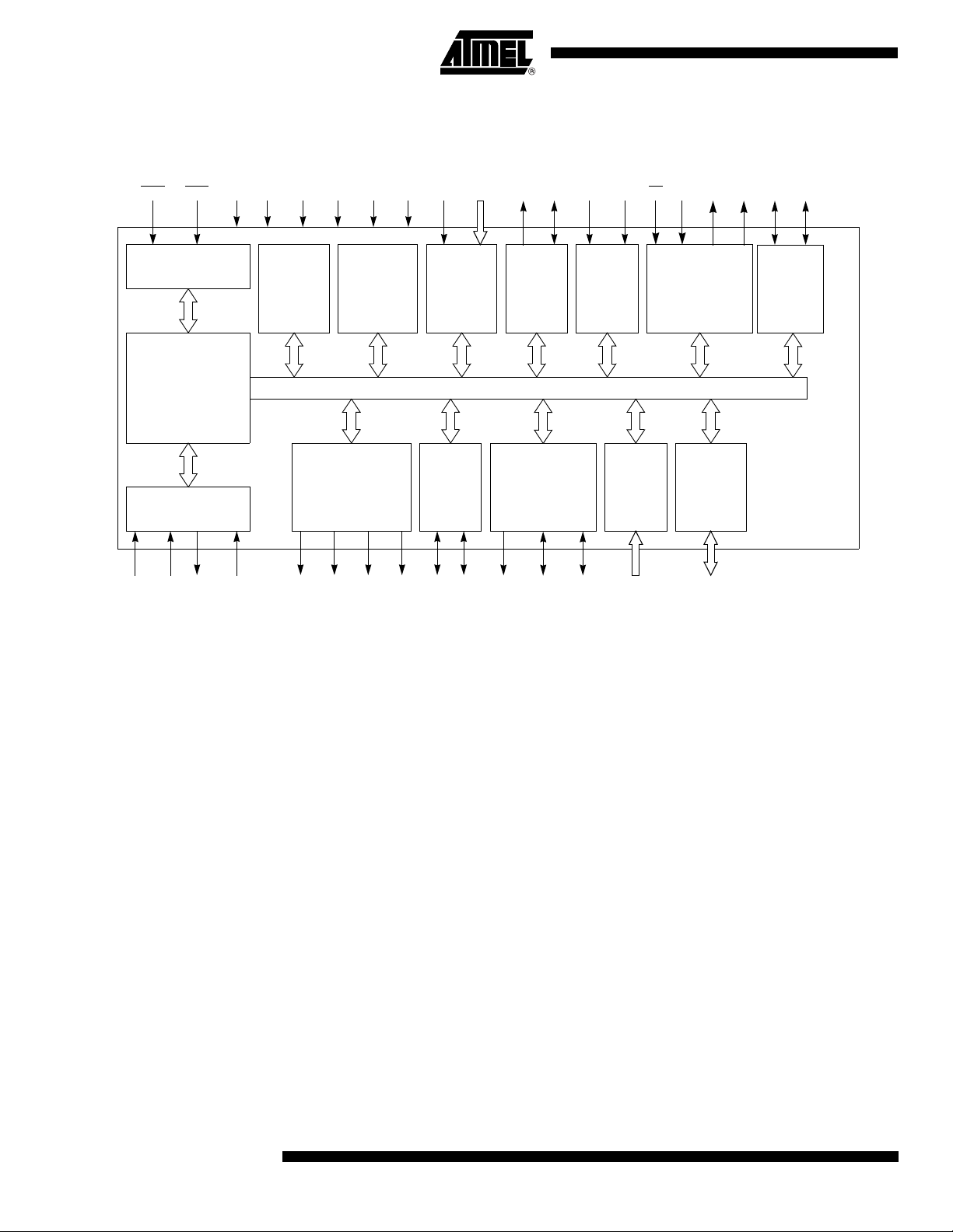
3. Block Diagram
8-BIT INTERNAL BUS
Clock and PLL
Unit
C51 (X2 CORE)
RAM
2304 Bytes
Flash
Interrupt
Handler Unit
FILT X2X1
MMC
Interface
I/O
MDAT
P0 - P5
10-bit A-to-D
Converter
V
SS
V
DD
Keyboard
Interface
KIN3:0
I2S/PCM
Audio Interface
AVSS
AV
DD
AIN1:0
Ports
INT0 INT1 MOSIMISO
Timers 0/1
T1T0
SPI/DataFlash
Controller
MCLK
MCMD
SCK
RST
AREF
DSELDCLK SCLKDOUT
64K Bytes
USB
Controller
D+ D-
UART
RXDTXD
IDE
Interface
SS
Watchdog
Flash Boot
4K Bytes
UVSS
UV
DD
and
BRG
1 1
1 1 11 2 2 2 2
3
TWI
Controller
SCL SDA
1 1
Figure 3-1. AT89C5132 Block Diagram
Notes: 1. Alternate function of Port 3
2. Alternate function of Port 4
3. Alternate function of Port 1
2
AT89C5132
4173E–USB–09/07
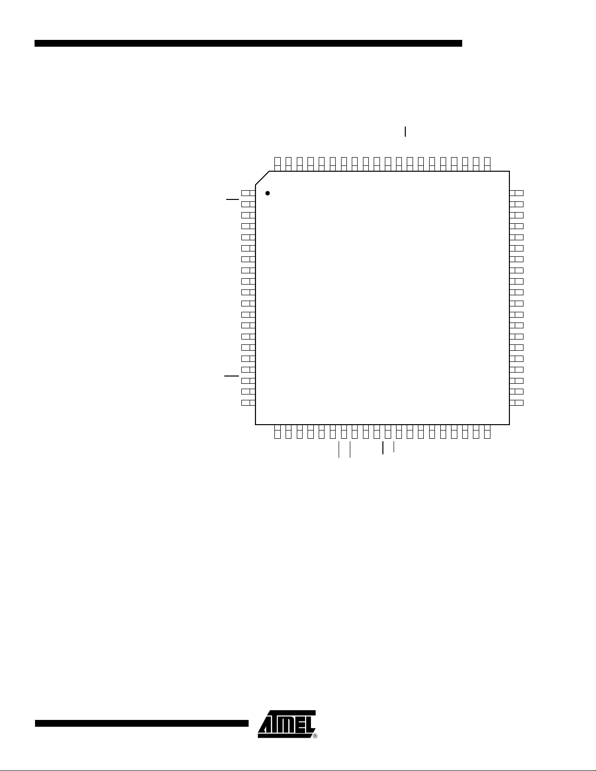
4. Pin Description
P0.3/AD3
P0.4/AD4
P0.5/AD5
VSS
VDD
P0.6/AD6
P0.7/AD7
P2.0/A8
P2.1/A9
P3.1/TXD
P3.2/INT0
P3.3/INT1
P3.4/T0
P3.0/RXD
1
2
3
4
5
6
7
8
13
11
10
P2.2/A10
P2.3/A11
P2.4/A12
P2.6/A14
P2.5/A13
P2.7/A15
MCLK
MDAT
MCMD
P0.2/AD2
P0.1/AD1
P0.0/AD0
PVSS
VSS
X2
X1
TST
VSS
9
12
14
15
16
P4.3/SS
P4.2/SCK
P4.1/MOSI
P4.0/MISO
VSS
VDD
RST
SCLK
DSEL
DCLK
DOUT
AIN1
AIN0
AREFN
AREFP
AVSS
AVDD
P3.7/RD
P3.6/WR
P3.5/T1
VDD
P1.0/KIN0
P1.1/KIN1
P1.2/KIN2
P1.3/KIN3
P1.4
P1.5
P1.7/SDA
FILT
PVDD
VDD
P1.6/SCL
17
18
19
20
21222324252627
28
33
31
302932
34353637383940
41
42
43
44
45
46
47
48
53
51
50
49
52
54
55
56
57
58
59
60
61
62
63
64
65
66
67
68
73
717069
72
74
75
76
77
78
79
80
ALE
ISP
UVDD
UVSS
P5.0
P5.1
P4.7
P4.6
D-
D+
P5.3
P5.2
VSS
VDD
P4.5
P4.4
TQFP80
Figure 4-1. AT89C5132 80-pin TQFP Package
AT89C5132
4173E–USB–09/07
3
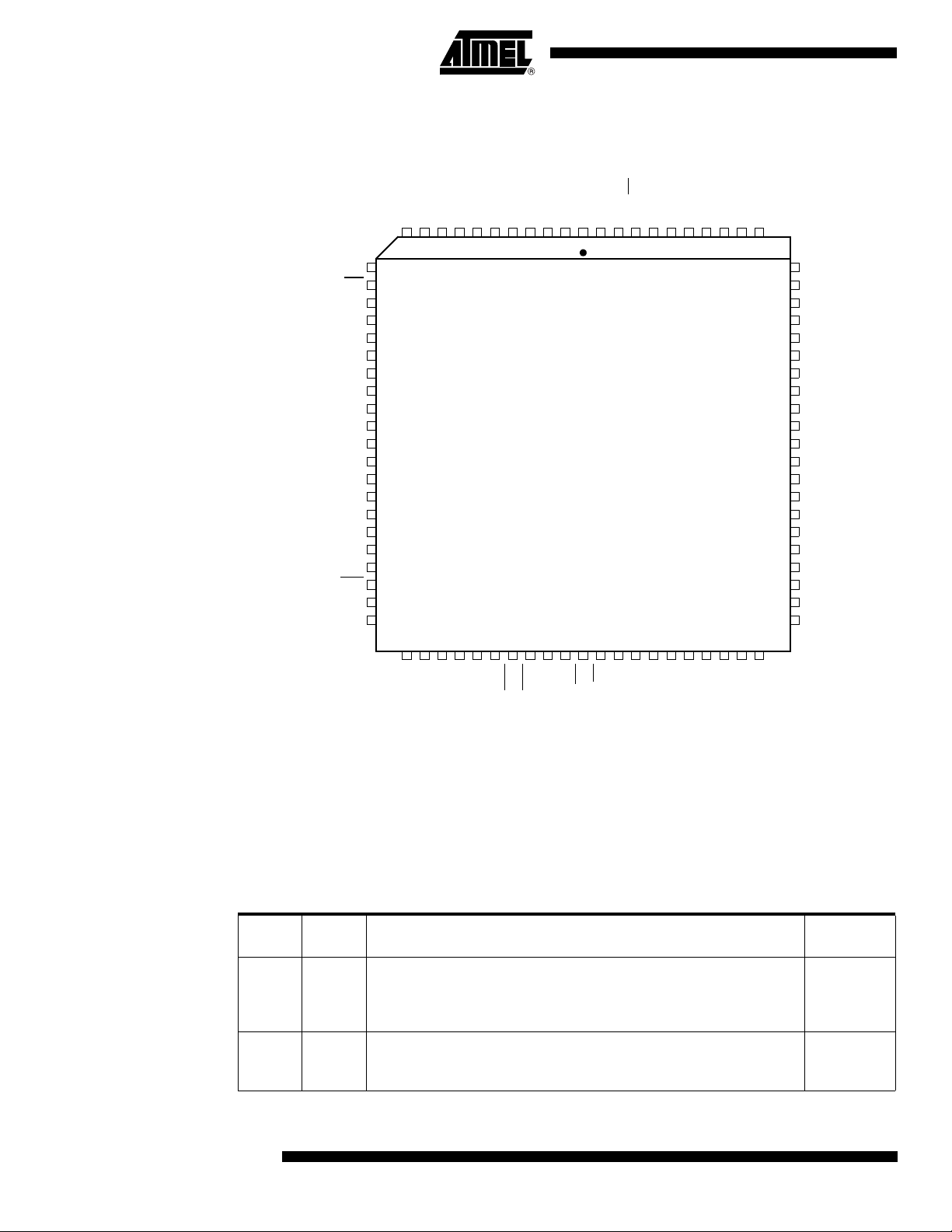
Figure 4-2. AT89C5132 84-pin PLCC
PLCC84
P0.3/AD3
P0.4/AD4
P0.5/AD5
VSS
VDD
P0.6/AD6
P0.7/AD7
P2.0/A8
P2.1/A9
P3.3/INT1
P3.4/T0
P3.5/T1
P3.6/WR
P3.2/INT0
65
64
63
62
61
60
59
58
55
56
57
12
13
14
15
16
17
22
20
19
3334353637
432
1
84838281807978
NC
P2.3/A11
P2.4/A12
P2.6/A14
P2.5/A13
P2.7/A15
MCLK
MDAT
MCMD
P0.2/AD2
P0.1/AD1
P5.0
PAVSS
VSS
X2
NC
X1
P3.1/TXD
18
21
23
24
25
3839404142
69
68
67
66
70
5
6
7
8
9
P4.3/SS
P4.2/SCK
P4.1/MOSI
P4.0/MISO
VSS
VDD
RST
SCLK
DSEL
DCLK
DOUT
AIN1
AIN0
AREFN
AREFP
AVSS
AVDD
VSS
VDD
P3.7/RD
P3.0/RXD
P1.0/KIN0
P1.1/KIN1
P1.2/KIN2
P1.3/KIN3
P1.4
P1.5
P1.7/SDA
FILT
PAVDD
VDD
P1.6/SCL
26
43
TST
P5.2
P0.0/AD0
77
P2.2/A10
54
ALE
ISP
NC
P5.1
P4.7
P4.6
76
75
10
11
28
27
29
30
31
32
UVDD
UVSS
444546474849505152
53
74
73
7271P4.4
P4.5
VDD
VSS
D-
D+
NC
P5.3
(1)
4.1 Signals
Note: 1. For development board only.
All the AT89C5132 signals are detailed by functionality in Table 1 to Table 14.
Table 1. Ports Signal Description
Signal
Name Type Description
P0.7:0 I/O
P1.7:0 I/O
Port 0
P0 is an 8-bit open-drain bidirectional I/O port. Port 0 pins that have 1s written
to them float and can be used as high impedance inputs. To avoid any parasitic
current consumption, floating P0 inputs must be polarized to V
Port 1
P1 is an 8-bit bidirectional I/O port with internal pull-ups.
DD
or VSS.
Alternate
Function
AD7:0
KIN3:0
SCL
SDA
4
AT89C5132
4173E–USB–09/07
AT89C5132
Signal
Name Type Description
P2.7:0 I/O
P3.7:0 I/O
P4.7:0 I/O
P5.3:0 I/O
Port 2
P2 is an 8-bit bidirectional I/O port with internal pull-ups.
Port 3
P3 is an 8-bit bidirectional I/O port with internal pull-ups.
Port 4
P4 is an 8-bit bidirectional I/O port with internal pull-ups.
Port 5
P5 is a 4-bit bidirectional I/O port with internal pull-ups.
Table 2. Clock Signal Description
Signal
Name Type Description
Input to the on-chip inverting oscillator amplifier
X1 I
To use the internal oscillator, a crystal/resonator circuit is connected to this pin.
If an external oscillator is used, its output is connected to this pin. X1 is the
clock source for internal timing.
Alternate
Function
A15:8
RXD
TXD
INT0
INT1
T0
T1
WR
RD
MISO
MOSI
SCK
SS
-
Alternate
Function
-
X2 O
FILT I
Output of the on-chip inverting oscillator amplifier
To use the internal oscillator, a crystal/resonator circuit is connected to this pin.
If an external oscillator is used, leave X2 unconnected.
PLL Low Pass Filter input
FILT receives the RC network of the PLL low pass filter.
Table 3. Timer 0 and Timer 1 Signal Description
Signal
Name Type Description
Timer 0 Gate Input
INT0 serves as external run control for timer 0, when selected by GATE0 bit in
TCON register.
INT0 I
INT1 I
External Interrupt 0
INT0 input sets IE0 in the TCON register. If bit IT0 in this register is set, bit IE0
is set by a falling edge on INT0. If bit IT0 is cleared, bit IE0 is set by a low level
on INT0.
Timer 1 Gate Input
INT1 serves as external run control for timer 1, when selected by GATE1 bit in
TCON register.
External Interrupt 1
INT1 input sets IE1 in the TCON register. If bit IT1 in this register is set, bit IE1
is set by a falling edge on INT1. If bit IT1 is cleared, bit IE1 is set by a low level
on INT1.
-
-
Alternate
Function
P3.2
P3.3
4173E–USB–09/07
5
Signal
Name Type Description
Alternate
Function
T0 I
T1 I
Timer 0 External Clock Input
When timer 0 operates as a counter, a falling edge on the T0 pin increments
the count.
Timer 1 External Clock Input
When timer 1 operates as a counter, a falling edge on the T1 pin increments
the count.
Table 4. Audio Interface Signal Description
Signal
Name Type Description
DCLK O DAC Data Bit Clock -
DOUT O DAC Audio Data -
DSEL O
SCLK O
DAC Channel Select Signal
DSEL is the sample rate clock output.
DAC System Clock
SCLK is the oversampling clock synchronized to the digital audio data (DOUT)
and the channel selection signal (DSEL).
Table 5. USB Controller Signal Description
Signal
Name Type Description
P3.4
P3.5
Alternate
Function
-
-
Alternate
Function
D+ I/O
D- I/O USB Negative Data Upstream Port -
USB Positive Data Upstream Port
This pin requires an external 1.5 KΩ pull-up to VDD for full speed operation.
Table 6. MutiMediaCard Interface Signal Description
Signal
Name Type Description
MCLK O
MCMD I/O
MDAT I/O
MMC Clock output
Data or command clock transfer.
MMC Command line
Bidirectional command channel used for card initialization and data transfer
commands. To avoid any parasitic current consumption, unused MCMD input
must be polarized to V
MMC Data line
Bidirectional data channel. To avoid any parasitic current consumption, unused
MDAT input must be polarized to VDD or VSS.
DD
or VSS.
-
Alternate
Function
-
-
-
6
AT89C5132
4173E–USB–09/07
Table 7. UART Signal Description
AT89C5132
Signal
Name Type Description
RXD I/O
TXD O
Receive Serial Data
RXD sends and receives data in serial I/O mode 0 and receives data in serial
I/O modes 1, 2 and 3.
Transmit Serial Data
TXD outputs the shift clock in serial I/O mode 0 and transmits data in serial I/O
modes 1, 2 and 3.
Table 8. SPI Controller Signal Description
Signal
Name Type Description
MISO I/O
MOSI I/O
SCK I/O
SS I
SPI Master Input Slave Output Data Line
When in master mode, MISO receives data from the slave peripheral. When in
slave mode, MISO outputs data to the master controller.
SPI Master Output Slave Input Data Line
When in master mode, MOSI outputs data to the slave peripheral. When in
slave mode, MOSI receives data from the master controller.
SPI Clock Line
When in master mode, SCK outputs clock to the slave peripheral. When in
slave mode, SCK receives clock from the master controller.
SPI Slave Select Line
When in controlled slave mode, SS enables the slave mode.
Alternate
Function
P3.0
P3.1
Alternate
Function
P4.0
P4.1
P4.2
P4.3
Table 9. TWI Controller Signal Description
Signal
Name Type Description
TWI Serial Clock
SCL I/O
SDA I/O
When TWI controller is in master mode, SCL outputs the serial clock to the
slave peripherals. When TWI controller is in slave mode, SCL receives clock
from the master controller.
TWI Serial Data
SDA is the bidirectional Two Wire data line.
Table 10. A/D Converter Signal Description
Signal
Name Type Description
AIN1:0 I A/D Converter Analog Inputs -
AREFP I Analog Positive Voltage Reference Input -
AREFN I
Analog Negative Voltage Reference Input
This pin is internally connected to AVSS.
Alternate
Function
P1.6
P1.7
Alternate
Function
-
4173E–USB–09/07
7
Table 11. Keypad Interface Signal Description
Signal
Name Type Description
KIN3:0 I
Keypad Input Lines
Holding one of these pins high or low for 24 oscillator periods triggers a
keypad interrupt.
Table 12. External Access Signal Description
Signal
Name Type Description
Address Lines
A15:8 I/O
AD7:0 I/O
ALE O
ISP I/O
Upper address lines for the external bus.
Multiplexed higher address and data lines for the IDE interface.
Address/Data Lines
Multiplexed lower address and data lines for the external memory or the IDE
interface.
Address Latch Enable Output
ALE signals the start of an external bus cycle and indicates that valid address
information is available on lines A7:0. An external latch is used to demultiplex
the address from address/data bus.
ISP Enable Input
This signal must be held to GND through a pull-down resistor at the falling
reset to force execution of the internal bootloader.
Alternate
Function
P1.3:0
Alternate
Function
P2.7:0
P0.7:0
-
-
RD O
WR O
Read Signal
Read signal asserted during external data memory read operation.
Write Signal
Write signal asserted during external data memory write operation.
Table 13. System Signal Description
Signal
Name Type Description
Reset Input
Holding this pin high for 64 oscillator periods while the oscillator is running
resets the device. The Port pins are driven to their reset conditions when a
RST I
TST I
voltage lower than VIL is applied, whether or not the oscillator is running.
This pin has an internal pull-down resistor which allows the device to be reset
by connecting a capacitor between this pin and VDD.
Asserting RST when the chip is in Idle mode or Power-Down mode returns the
chip to normal operation.
Test Input
Test mode entry signal. This pin must be set to VDD.
P3.7
P3.6
Alternate
Function
-
-
8
AT89C5132
4173E–USB–09/07

Table 14. Power Signal Description
AT89C5132
Signal
Name Type Description
VDD PWR
VSS GND
AVDD PWR
AVSS GND
PVDD PWR
PVSS GND
UVDD PWR
UVSS GND
Digital Supply Voltage
Connect these pins to +3V supply voltage.
Circuit Ground
Connect these pins to ground.
Analog Supply Voltage
Connect this pin to +3V supply voltage.
Analog Ground
Connect this pin to ground.
PLL Supply voltage
Connect this pin to +3V supply voltage.
PLL Circuit Ground
Connect this pin to ground.
USB Supply Voltage
Connect this pin to +3V supply voltage.
USB Ground
Connect this pin to ground.
Alternate
Function
-
-
-
-
-
-
-
-
4173E–USB–09/07
9
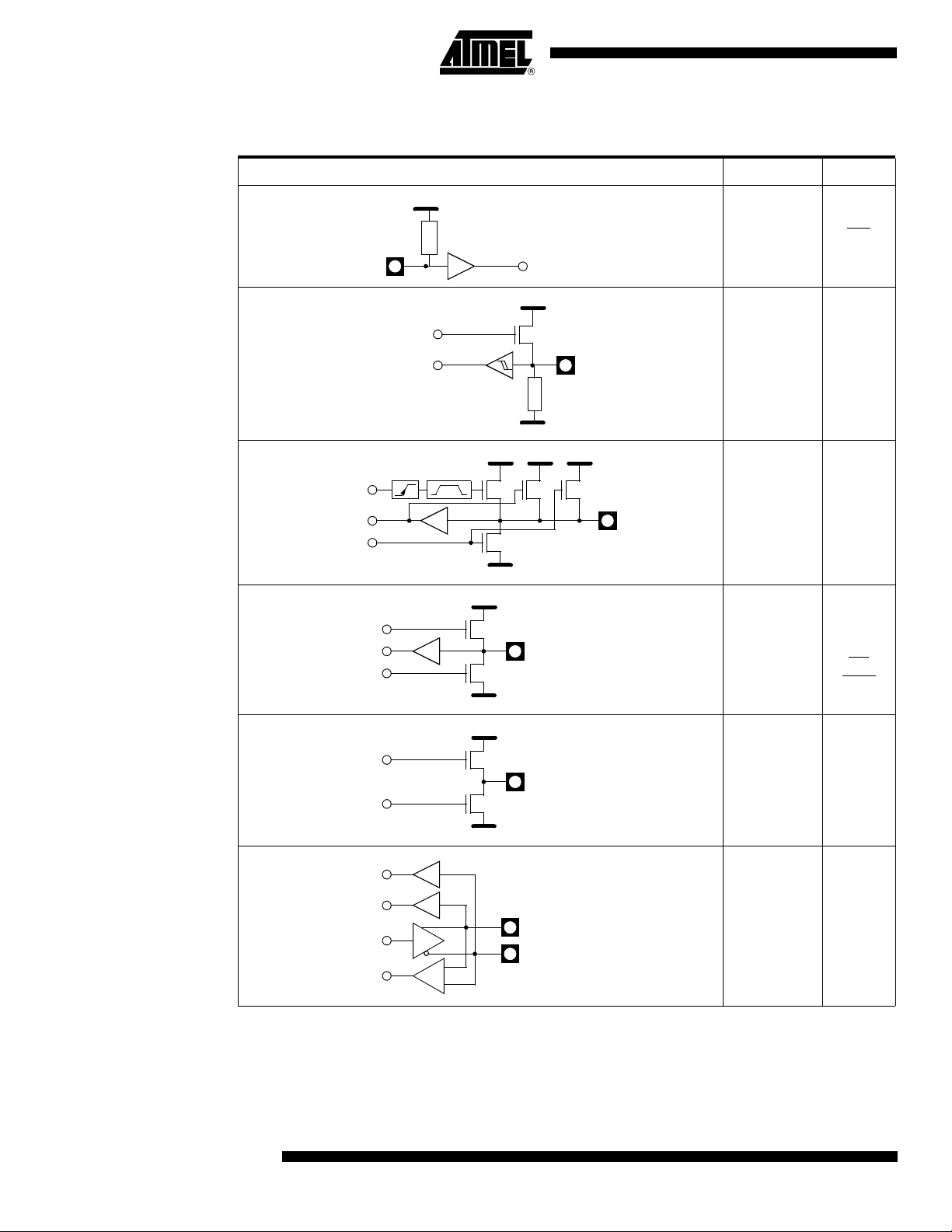
4.2 Internal Pin Structure
R
TST
VDD
R
RST
VSS
P
VDD
Watchdog Output
P
3
VSS
N
P
1
VDD VDD
2 osc
Latch Output
periods
P
2
VDD
VSS
N
P
VDD
VSS
N
P
VDD
D+
D-
Table 15. Detailed Internal Pin Structure
Circuit
(1)
Type Pins
Input TST
Input/Output RST
(2)
P1
(3)
Input/Output
P2
P3
P4
P53:0
10
Notes: 1. For information on resistors value, input/output levels, and drive capability, refer to the
AT89C5132
P0
MCMD
Input/Output
MDAT
ISP
PSEN
ALE
SCLK
DCLK
Output
DOUT
DSEL
MCLK
Input/Output
D+
D-
Section “DC Characteristics”, page 183.
2. When the Two Wire controller is enabled, P1, P2, and P3 transistors are disabled allowing
pseudo open-drain structure.
3. In Port 2, P1 transistor is continuously driven when outputting a high level bit address (A15:8).
4173E–USB–09/07

5. Address Spaces
The AT8xC5132 derivatives implement four different address spaces:
• Program/Code Memory
• Boot Memory
• Data Memory
• Special Function Registers (SFRs)
5.0.1 Code Memory
The AT89C5132 implements 64K Bytes of on-chip program/code memory in Flash technology.
The Flash memory increases ROM functionality by enabling in-circuit electrical erasure and programming. Thanks to the internal charge pump, the high voltage needed for programming or
erasing Flash cells is generated on-chip using the standard V
can be programmed using only one voltage and allows in application software programming
commonly known as IAP. Hardware programming mode is also available using specific programming tools.
5.0.2 Boot Memory
The AT89C5132 implements 4K Bytes of on-chip boot memory provided in Flash technology.
This boot memory is delivered programmed with a standard bootloader software allowing in system programming commonly known as ISP. It also contains some Application Programming
Interfaces routines commonly known as API allowing user to develop his own bootloader.
AT89C5132
DD
voltage. Thus, the AT89C5132
5.0.3 Data Memory
The AT89C5132 derivatives implement 2304 bytes of on-chip data RAM. This memory is divided
in two separate areas:
• 256 bytes of on-chip RAM memory (standard C51 memory).
• 2048 bytes of on-chip expanded RAM memory (ERAM accessible via MOVX instructions).
4173E–USB–09/07
11
6. Clock Controller
X1
X2
PD
PCON.1
IDL
PCON.0
Peripheral
CPU Core
0
1
X2
CKCON.0
÷
2
PER
CLOCK
Clock
Clock
Peripheral Clock Symbol
CPU
CLOCK
CPU Core Clock Symbol
OSC
CLOCK
Oscillator Clock Symbol
Oscillator
Clock
V
SS
X1
X2
Q
C1
C2
The AT89C5132 clock controller is based on an on-chip oscillator feeding an on-chip Phase
Lock Loop (PLL). All internal clocks to the peripherals and CPU core are generated by this
controller.
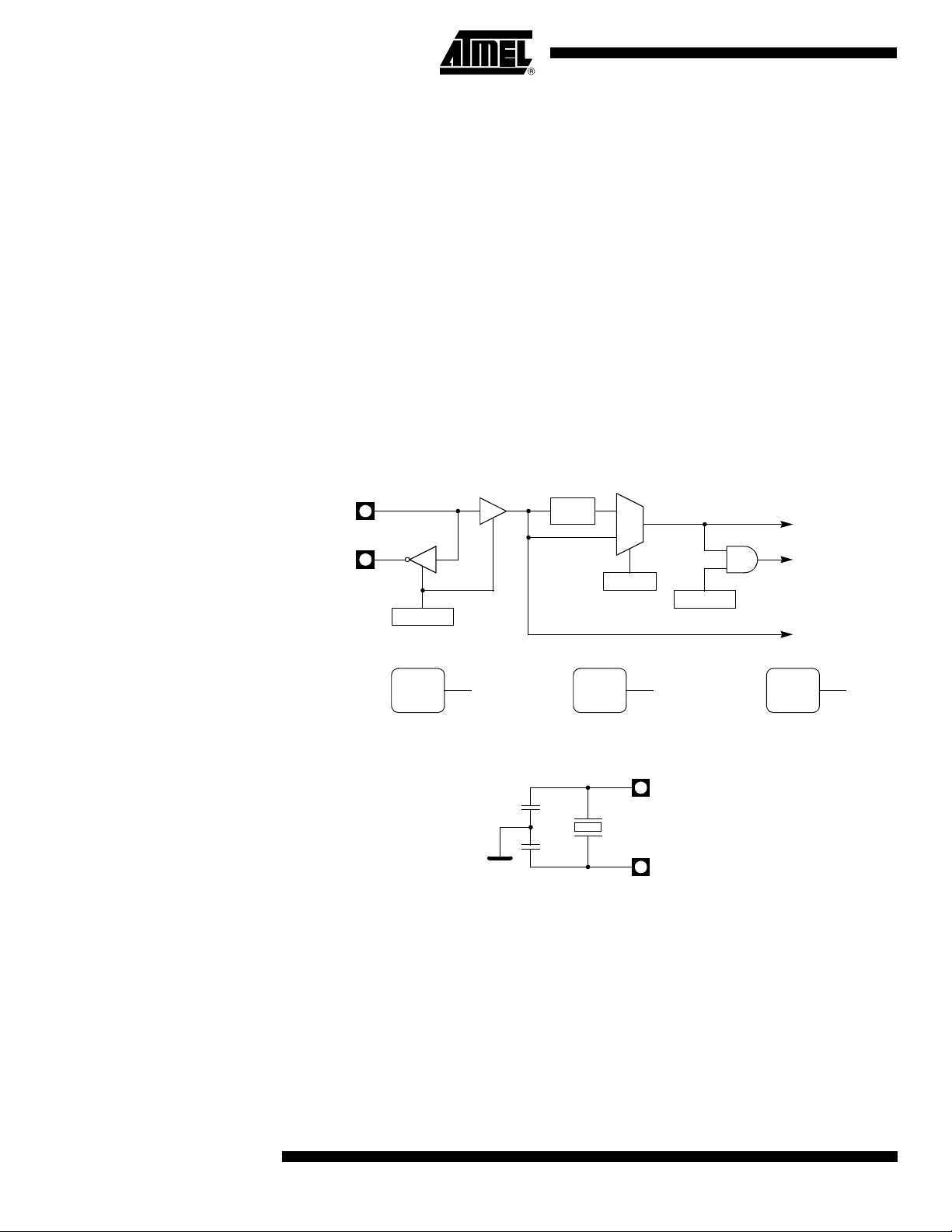
6.1 Oscillator
The AT89C5132 X1 and X2 pins are the input and the output of a single-stage on-chip inverter
(see Figure 6-1) that can be configured with off-chip components such as a Pierce oscillator
(see Figure 6-2). Value of capacitors and crystal characteristics are detailed in the Section “DC
Characteristics”.
The oscillator outputs three different clocks: a clock for the PLL, a clock for the CPU core, and a
clock for the peripherals as shown in Figure 6-1. These clocks are either enabled or disabled,
depending on the power reduction mode as detailed in the section“Power Management” on
page 44. The peripheral clock is used to generate the Timer 0, Timer 1, MMC, ADC, SPI, and
Port sampling clocks.
Figure 6-1. Oscillator Block Diagram and Symbol
6.2 X2 Feature
12
AT89C5132
Figure 6-2. Crystal Connection
Unlike standard C51 products that require 12 oscillator clock periods per machine cycle, the
AT89C5132 needs only 6 oscillator clock periods per machine cycle. This feature called the “X2
(1)
in CKCON (see Table 1) and allows the AT89C5132
4173E–USB–09/07
feature” can be enabled using the X2 bit
to operate in 6 or 12 oscillator clock periods per machine cycle. As shown in Figure 6-1, both
CPU and peripheral clocks are affected by this feature. Figure 6-3 shows the X2 mode switching
waveforms. After reset, the standard mode is activated. In standard mode, the CPU and periph-
AT89C5132
X1 ÷ 2
X1
Clock
X2 Bit
X2 Mode
(1)
STD Mode STD Mode
eral clock frequency is the oscillator frequency divided by 2 while in X2 mode, it is the oscillator
frequency.
Note: 1. The X2 bit reset value depends on the X2B bit in the Hardware Security Byte (see Table 12 on
page 24). Using the AT89C5132 (Flash Version) the system can boot either in standard or X2
mode depending on the X2B value. Using AT83C51SND1C (ROM Version) the system always
boots in standard mode. X2B bit can be changed to X2 mode later by software.
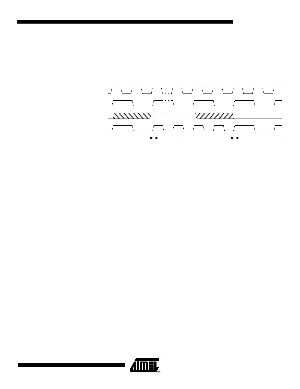
Figure 6-3. Mode Switching Waveforms
Note: In order to prevent any incorrect operation while operating in X2 mode, the user must be aware
that all peripherals using clock frequency as time reference (timers…) will have their time reference divided by two. For example, a free running timer generating an interrupt every 20 ms will
then generate an interrupt every 10 ms.
6.3 PLL
6.3.1 PLL Description
The AT89C5132 PLL is used to generate internal high frequency clock (the PLL Clock) synchronized with an external low-frequency (the Oscillator Clock). The PLL clock provides the audio
interface, and the USB interface clocks. Figure 6-4 shows the internal structure of the PLL.
The PFLD block is the Phase Frequency Comparator and Lock Detector. This block makes the
comparison between the reference clock coming from the N divider and the reverse clock coming from the R divider and generates some pulses on the Up or Down signal depending on the
edge position of the reverse clock. The PLLEN bit in PLLCON register is used to enable the
clock generation. When the PLL is locked, the bit PLOCK in PLLCON register (see Table 3) is
set.
The CHP block is the Charge Pump that generates the voltage reference for the VCO by injecting or extracting charges from the external filter connected on PFILT pin (see Figure 6-5). Value
of the filter components are detailed in the Section “DC Characteristics”.
The VCO block is the Voltage Controlled Oscillator controlled by the voltage V
produced by the
ref
charge pump. It generates a square wave signal: the PLL clock.
4173E–USB–09/07
13
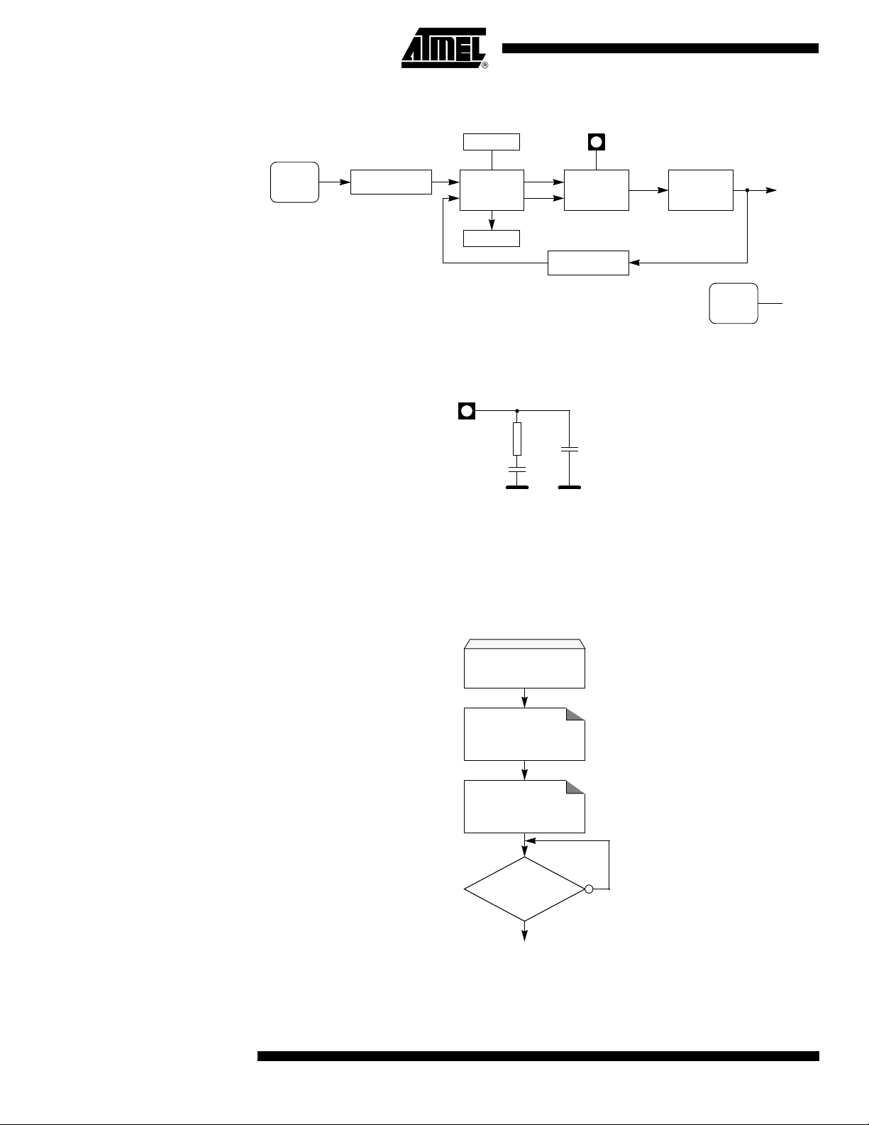
Figure 6-4. PLL Block Diagram and Symbol
PLLEN
PLLCON.1
N6:0
N divider
R divider
VCO
PLLclk
OSCclk R 1+( )
×
N 1+
-----------------------------------------------=
OSC
CLOCK
PFLD
PLOCK
PLLCON.0
PFILT
CHP
Vref
Up
Down
R9:0
PLL
CLOCK
PLL Clock Symbol
PLL
Clock
V
SS
PFILT
R
C1
C2
V
SS
PLL
Programming
Configure Dividers
N6:0 = xxxxxxb
R9:0 = xxxxxxxxxxb
Enable PLL
PLLRES = 0
PLLEN = 1
PLL Locked?
PLOCK = 1?
Figure 6-5. PLL Filter Connection
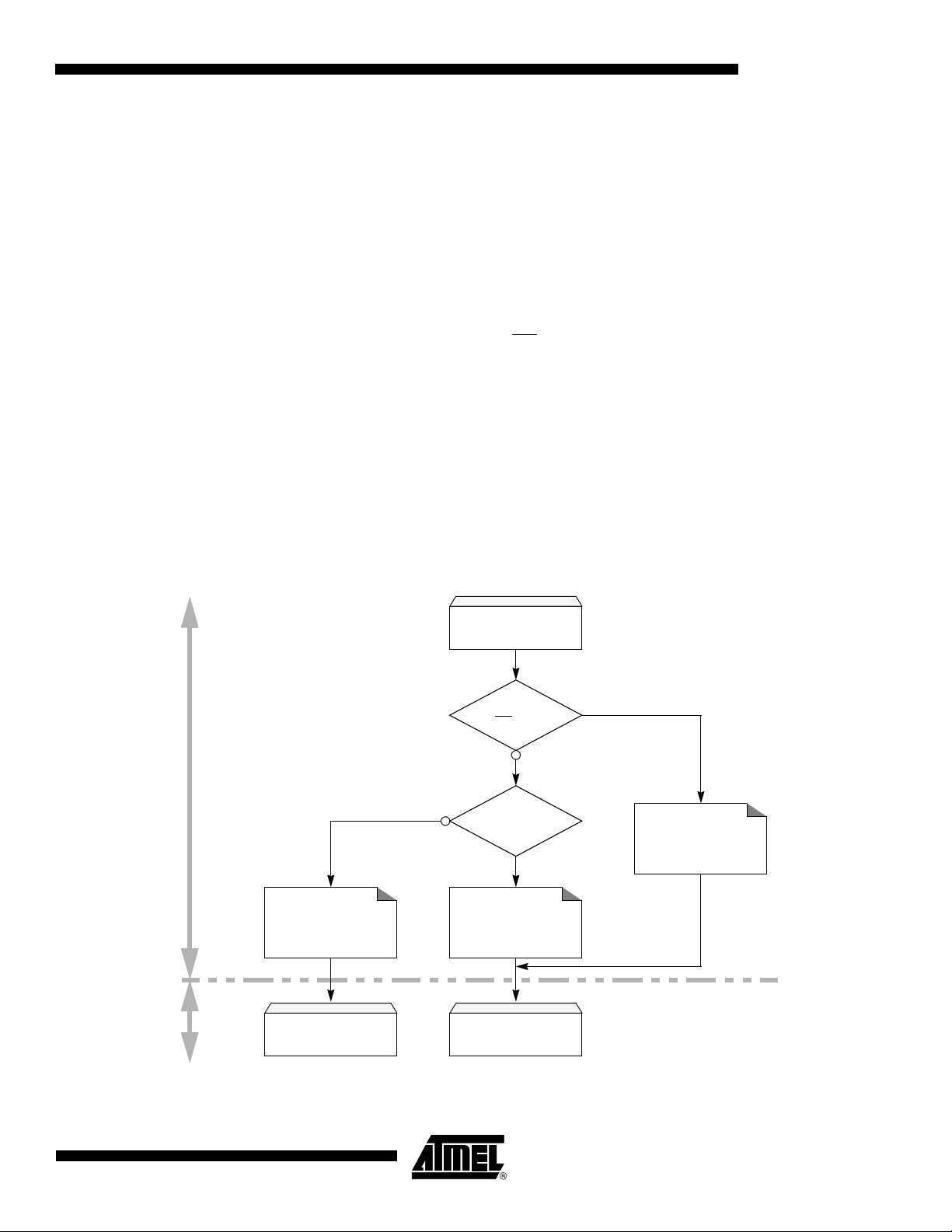
6.3.2 PLL Programming
The PLL is programmed using the flow shown in Figure 6-6. As soon as clock generation is
enabled, the user must wait until the lock indicator is set to ensure the clock output is stable. The
PLL clock frequency will depend on the audio interface clock frequencies.
Figure 6-6. PLL Programming Flow
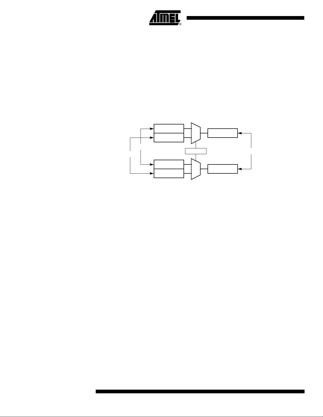
6.4 Registers
Table 1. CKCON Register
14
AT89C5132
4173E–USB–09/07
AT89C5132
CKCON (S:8Fh) – Clock Control Register
7 6 5 4 3 2 1 0
TWIX2 WDX2 - SIX2 - T1X2 T0X2 X2
Bit Number
7 TWIX2
6 WDX2
5 -
4 SIX2
3 -
2 T1X2
1 T0X2
0 X2
Bit
Mnemonic Description
Two-Wire Clock Control Bit
Set to select the oscillator clock divided by 2 as TWI clock input (X2 independent).
Clear to select the peripheral clock as TWI clock input (X2 dependent).
Watchdog Clock Control Bit
Set to select the oscillator clock divided by 2 as watchdog clock input (X2 independent).
Clear to select the peripheral clock as watchdog clock input (X2 dependent).
Reserved
The value read from this bit is indeterminate. Do not set this bit.
Enhanced UART Clock (Mode 0 and 2) Control Bit
Set to select the oscillator clock divided by 2 as UART clock input (X2 independent).
Clear to select the peripheral clock as UART clock input (X2 dependent)..
Reserved
The value read from this bit is indeterminate. Do not set this bit.
Timer 1 Clock Control Bit
Set to select the oscillator clock divided by two as Timer 1 clock input (X2 independent).
Clear to select the peripheral clock as Timer 1 clock input (X2 dependent).
Timer 0 Clock Control Bit
Set to select the oscillator clock divided by two as timer 0 clock input (X2 independent).
Clear to select the peripheral clock as timer 0 clock input (X2 dependent).
System Clock Control Bit
Clear to select 12 clock periods per machine cycle (STD mode, F
Set to select 6 clock periods per machine cycle (X2 mode, F
Reset Value = 0000 000Xb
CPU
CPU
= F
= F
PER
= F
PER
= F
OSC
/
2).
OSC
).
4173E–USB–09/07
Table 2. PLLNDIV Register
PLLNDIV (S:EEh) – PLL N Divider Register
7 6 5 4 3 2 1 0
- N6 N5 N4 N3 N2 N1 N0
Bit Number
7 -
6-0 N6:0
Bit
Mnemonic Description
Reserved
The value read from this bit is always 0. Do not set this bit.
PLL N Divider
7-bit N divider.
Reset Value = 0000 0000b
15
Table 3. PLLCON Register
PLLCON (S:E9h) – PLL Control Register
7 6 5 4 3 2 1 0
R1 R0 - - PLLRES - PLLEN PLOCK
Bit Number
7 - 6 R1:0
5 - 4 -
3 PLLRES
2 -
1 PLLEN
0 PLOCK
Bit
Mnemonic Description
PLL Least Significant Bits R Divider
2 LSB of the 10-bit R divider.
Reserved
The values read from these Bits are always 0. Do not set these Bits.
PLL Reset Bit
Set this bit to reset the PLL.
Clear this bit to free the PLL and allow enabling.
Reserved
The values read from this bit is always 0. Do not set this bit.
PLL Enable Bit
Set to enable the PLL.
Clear to disable the PLL.
PLL Lock Indicator
Set by hardware when PLL is locked.
Clear by hardware when PLL is unlocked.
Reset Value = 0000 1000b
Table 4. PLLRDIV Register
PLLRDIV (S:EFh) – PLL R Divider Register
7 6 5 4 3 2 1 0
R9 R8 R7 R6 R5 R4 R3 R2
Bit Number
7 - 0 R9:2
Bit
Mnemonic Description
PLL Most Significant Bits R Divider
8 MSB of the 10-bit R divider.
Reset Value = 0000 0000b
16
AT89C5132
4173E–USB–09/07
7. Program/Code Memory
4K Bytes
Boot Flash
FFFFh
F000h
0000h
64K Bytes
Code Flash
FFFFh
F000h
FFFFh
64K Bytes
Flash Memory
0000h
Hardware Security
User
4K Bytes
Flash Memory
FFFFh
F000h
Boot
Extra Row
The AT89C5132 implements 64K Bytes of on-chip program/code memory. Figure 7-1 shows the
split of internal and external program/code memory spaces depending on the product.
The Flash memory increases EPROM and ROM functionality by in-circuit electrical erasure and
programming. The high voltage needed for programming or erasing Flash cells is generated onchip using the standard VDD voltage, made possible by the internal charge pump. Thus, the
AT89C5132 can be programmed using only one voltage and allows in application software programming. Hardware programming mode is also available using common programming tools.
See the application note ‘Programming T89C51x and AT89C51x with Device Programmers’.
The AT89C5132 implements an additional 4K Bytes of on-chip boot Flash memory provided in
Flash memory. This boot memory is delivered programmed with a standard bootloader software
allowing In-System Programming (ISP). It also contains some Application Programming Interfaces (API), allowing In Application Programming (IAP) by using user’s own bootloader.
Figure 7-1. Program/Code Memory Organization
AT89C5132
7.1 Flash Memory Architecture
As shown in Figure 7-2 the AT89C5132 Flash memory is composed of four spaces detailed in
the following paragraphs.
Figure 7-2. AT89C5132 Memory Architecture
4173E–USB–09/07
17

7.1.1 User Space
This space is composed of a 64K Bytes Flash memory organized in 512 pages of 128 Bytes. It
contains the user’s application code. This space can be read or written by both software and
hardware modes.
7.1.2 Boot Space
This space is composed of a 4K Bytes Flash memory. It contains the bootloader for In-System
Programming and the routines for In-System Application Programming.
This space can only be read or written by hardware mode using a parallel programming tool.
7.1.3 Hardware Security Space
This space is composed of one byte: the Hardware Security Byte (HSB see Table 7) divided in
two separate nibbles see Table 7. The MSN contains the X2 mode configuration bit and the Boot
Loader Jump Bit as detailed in section “Boot Memory Execution” and can be written by software
while the LSN contains the lock system level to protect the memory content against piracy as
detailed in section “Hardware Security System” and can only be written by hardware.
7.1.4 Extra Row Space
This space is composed of two Bytes:
• The Software Boot Vector (SBV see Table 8).
This byte is used by the software bootloader to build the boot address.
• The Software Security Byte (SSB see Figure ).
This byte is used to lock the execution of some bootloader commands.
7.2 Hardware Security System
The AT89C5132 implements three lock Bits LB2:0 in the LSN of HSB (see Table 7) providing
three levels of security for user’s program as described in Table 7 while the AT83C51SND1C is
always set in read disabled mode.
• Level 0 is the level of an erased part and does not enable any security feature.
• Level 1 locks the hardware programming of both user and boot memories.
• Level 2 locks hardware verifying of both user and boot memories.
• Level 3 locks the external execution.
Table 5. Lock Bit Features
Level LB2
0 U U U Enable Enable Enable Enable Enable
1 U U P Enable Enable Enable Disable Enable
2 U P X Enable Enable Disable Disable Enable
(3)
3
Notes: 1. U means unprogrammed, P means programmed and X means don’t care (programmed or
(2)
P X X Enable Disable Disable Disable Enable
unprogrammed).
2. LB2 is not implemented in the AT89C5132 products.
3. AT89C5132 products are delivered with third level programmed to ensure that the code programmed by software using ISP or user’s bootloader is secured from any hardware piracy.
LB1 LB0
(1)
Internal
Execution
External
Execution
Hardware
Verifying
Hardware
Programming
Software
Programming
18
AT89C5132
4173E–USB–09/07
7.3 Boot Memory Execution
Atmel’s
Boot Loader
HardwareSoftware
Hard Cond?
ISP = L?
RESET
Hard Cond Init
ENBOOT = 1
PC = F000h
FCON = 00h
Prog Cond?
BLJB = P?
Standard Init
ENBOOT = 0
PC = 0000h
FCON = F0h
Prog Cond Init
ENBOOT = 1
PC = F000h
FCON = F0h
User’s
Application
Process Process
As internal C51 code space is limited to 64K Bytes, some mechanisms are implemented to allow
boot memory to be mapped in the code space for execution at addresses from F000h to FFFFh.
The boot memory is enabled by setting the ENBOOT bit in AUXR1 (see Table 6). The three
ways to set this bit are detailed in the following sections.
7.3.1 Software Boot Mapping
The software way to set ENBOOT consists in writing to AUXR1 from the user’s software. This
enables bootloader or API routines execution.
7.3.2 Hardware Condition Boot Mapping
The hardware condition is based on the ISP pin. When driving this pin to low level, the chip reset
sets ENBOOT and forces the reset vector to F000h instead of 0000h in order to execute the
bootloader software.
As shown in Figure 7-3, the hardware condition always allows in-system recovery when user’s
memory has been corrupted.
7.3.3 Programmed Condition Boot Mapping
The programmed condition is based on the Bootloader Jump Bit (BLJB) in HSB. As shown in
Figure 7-3, when this bit is programmed (by hardware or software programming mode), the chip
resets ENBOOT and forces the reset vector to F000h instead of 0000h, in order to execute the
bootloader software.
AT89C5132
Figure 7-3. Hardware Boot Process Algorithm
4173E–USB–09/07
The software process (bootloader) is detailed in the AT89C5132 Bootloader datasheet.
19
7.3.4 Preventing Flash Corruption
See “Reset Recommendation to Prevent Flash Corruption” on page 45.
7.4 Registers
Table 6. AUXR1 Register
AUXR1 (S:A2h) – Auxiliary Register 1
7 6 5 4 3 2 1 0
- - ENBOOT - GF3 0 - DPS
Reset Value = XXXX 00X0b
7.5 Hardware Bytes
Table 7. HSB Byte – Hardware Security Byte
Bit Number
7 - 6 -
5 ENBOOT
4 -
3 GF3
2 0
1 - Reserved for Data Pointer Extension.
0 DPS
Bit
Mnemonic Description
Reserved
The values read from these Bits are indeterminate. Do not set these Bits.
Enable Boot Flash
Set this bit to map the boot Flash in the code space between at addresses F000h to
FFFFh.
Clear this bit to disable boot Flash.
Reserved
The values read from this bit is indeterminate. Do not set this bit.
General Flag
This bit is a general-purpose user flag.
Always Zero
This bit is stuck to logic 0 to allow INC AUXR1 instruction without affecting GF3 flag.
Data Pointer Select Bit
Set to select second data pointer: DPTR1.
Clear to select first data pointer: DPTR0.
20
X2B BLJB - - - LB2 LB1 LB0
Bit Number
5 - 4 -
AT89C5132
7 6 5 4 3 2 1 0
Bit
Mnemonic Description
X2 Bit
7 X2B
6 BLJB
3 -
(1)
Program this bit to start in X2 mode.
Unprogram (erase) this bit to start in standard mode.
Boot Loader Jump Bit
(2)
Program this bit to execute the boot loader at address F000h on next reset.
Unprogram (erase) this bit to execute user’s application at address 0000h on next reset.
Reserved
The value read from these bits is always unprogrammed. Do not program these bits.
Reserved
The value read from this bit is always unprogrammed. Do not program this bit.
4173E–USB–09/07
Bit Number
AT89C5132
Bit
Mnemonic Description
2 - 0 LB2:0
Hardware Lock Bits
Refer to for bits description.
Reset Value = XXUU UXXX, UUUU UUUU after an hardware full chip erase.
Note: 1. X2B initializes the X2 bit in CKCON during the reset phase.
2. In order to ensure boot loader activation at first power-up, AT89C5132 products are delivered
with BLJB programmed.
3. Bits 0 to 3 (LSN) can only be programmed by hardware mode.
Table 8. SBV Byte – Software Boot Vector
7 6 5 4 3 2 1 0
ADD15 ADD14 ADD13 ADD12 ADD11 ADD10 ADD9 ADD8
Bit Number
7 - 0 ADD15:8
Bit
Mnemonic Description
MSB of the user ’s bootloader 16-bit address location
Refer to the bootloader datasheet for usage information (bootloader dependent).
Reset Value = XXXX XXXX, UUUU UUUU after an hardware full chip erase.
Table 9. SSB Byte – Software Security Byte
7 6 5 4 3 2 1 0
SSB7 SSB6 SSB5 SSB4 SSB3 SSB2 SSB1 SSB0
Bit Number
7 - 0 SSB7:0
Bit
Mnemonic Description
Software Security Byte Data
Refer to the bootloader datasheet for usage information (bootloader dependent).
Reset Value = XXXX XXXX, UUUU UUUU after an hardware full chip erase.
4173E–USB–09/07
21

8. Data Memory
2K Bytes
Upper
128 Bytes
Internal RAM
Lower
128 Bytes
Internal RAM
Special
Function
Registers
80h 80h
00h
7FFh FFh
00h
FFh
64K Bytes
External XRAM
0000h
FFFFh
direct addressing
addressing
0800h
7Fh
Internal ERAM
direct or indirect
indirect addressing
EXTRAM = 0
EXTRAM = 1
The AT89C5132 provides data memory access in two different spaces:
1. The internal space mapped in three separate segments:
– The lower 128 Bytes RAM segment
– The upper 128 Bytes RAM segment
– The expanded 2048 Bytes RAM segment
2. The external space.
A fourth internal segment is available but dedicated to Special Function Registers, SFRs,
(addresses 80h to FFh) accessible by direct addressing mode. For information on this segment,
refer to the section “Special Function Registers”, page 29.
Figure 8-1 shows the internal and external data memory spaces organization.
Figure 8-1. Internal and External Data Memory Organization
8.1 Internal Space
8.1.1 Lower 128 Bytes RAM
The lower 128 Bytes of RAM (see Figure 8-2) are accessible from address 00h to 7Fh using
direct or indirect addressing modes. The lowest 32 Bytes are grouped into 4 banks of 8 registers
(R0 to R7). Two Bits RS0 and RS1 in PSW register (see Table 13) select which bank is in use
according to Table 10. This allows more efficient use of code space, since register instructions
are shorter than instructions that use direct addressing, and can be used for context switching in
interrupt service routines.
Table 10. Register Bank Selection
22
AT89C5132
RS1 RS0 Description
0 0 Register bank 0 from 00h to 07h
0 1 Register bank 1 from 08h to 0Fh
1 0 Register bank 2 from 10h to 17h
1 1 Register bank 3 from 18h to 1Fh
4173E–USB–09/07
The next 16 Bytes above the register banks form a block of bit-addressable memory space. The
Bit-Addressable Space
4 Banks of
8 Registers
R0 - R7
30h
7Fh
(Bit Addresses 0 - 7Fh)
20h
2Fh
18h
1Fh
10h
17h
08h
0Fh
00h
07h
C51 instruction set includes a wide selection of single-bit instructions, and the 128 Bits in this
area can be directly addressed by these instructions. The bit addresses in this area are 00h to
7Fh.
Figure 8-2. Lower 128 Bytes Internal RAM Organization
8.1.2 Upper 128 Bytes RAM
The upper 128 Bytes of RAM are accessible from address 80h to FFh using only indirect
addressing mode.
AT89C5132
8.1.3 Expanded RAM
8.2 External Space
The on-chip 2K Bytes of expanded RAM (ERAM) are accessible from address 0000h to 07FFh
using indirect addressing mode through MOVX instructions. In this address range, EXTRAM bit
in AUXR register (see Table 14) is used to select the ERAM (default) or the XRAM. As shown in
Figure 8-1 when EXTRAM = 0, the ERAM is selected and when EXTRAM = 1, the XRAM is
selected, See “External Space” on page 23.
The ERAM memory can be resized using XRS1:0 Bits in AUXR register to dynamically increase
external access to the XRAM space. Table 11 details the selected ERAM size and address
range.
Table 11. ERAM Size Selection
XRS1 XRS0 ERAM Size Address
0 0 256 Bytes 0 to 00FFh
0 1 512 Bytes 0 to 01FFh
1 0 1K Byte 0 to 03FFh
1 1 2K Bytes 0 to 07FFh
Note: Lower 128 Bytes RAM, Upper 128 Bytes RAM, and expanded RAM are made of volatile memory
cells. This means that the RAM content is indeterminate after power-up and must then be initialized properly.
8.2.1 Memory Interface
4173E–USB–09/07
The external memory interface comprises the external bus (port 0 and port 2) as well as the bus
control signals (RD, WR, and ALE).
23
Figure 8-3 shows the structure of the external address bus. P0 carries address A7:0 while P2
RAM
PERIPHERAL
AT89C5132
P2
P0
AD7:0
A15:8
A7:0
A15:8
D7:0
A7:0
ALE
WR
OERD
WR
Latch
carries address A15:8. Data D7:0 is multiplexed with A7:0 on P0. Table 12 describes the external memory interface signals.
Figure 8-3. External Data Memory Interface Structure
Table 12. External Data Memory Interface Signals
Signal
Name Type Description
A15:8 O
AD7:0 I/O
8.2.2 Page Access Mode
The AT89C5132 implement a feature called Page Access that disables the output of DPH on P2
when executing MOVX @DPTR instruction. Page Access is enable by setting the DPHDIS bit in
AUXR register.
Page Access is useful when application uses both ERAM and 256 Bytes of XRAM. In this case,
software modifies intensively EXTRAM bit to select access to ERAM or XRAM and must save it
if used in interrupt service routine. Page Access allows external access above 00FFh address
without generating DPH on P2. Thus ERAM is accessed using MOVX @Ri or MOVX @DPTR
with DPTR < 0100h, < 0200h, < 0400h or < 0800h depending on the XRS1:0 bits value. Then
XRAM is accessed using MOVX @DPTR with DPTR ≥ 0800h regardless of XRS1:0 bits value
while keeping P2 for general I/O usage.
ALE O
RD O
WR O
Address Lines
Upper address lines for the external bus.
Address/Data Lines
Multiplexed lower address lines and data for the external memory.
Address Latch Enable
ALE signals indicates that valid address information are available on lines AD7:0.
Read
Read signal output to external data memory.
Write
Write signal output to external memory.
Alternate
Function
P2.7:0
P0.7:0
-
P3.7
P3.6
8.2.3 External Bus Cycles
24
AT89C5132
This section describes the bus cycles that AT89C5132 executes to read (see Figure 8-4), and
write data (see Figure 8-5) in the external data memory.
4173E–USB–09/07
AT89C5132
ALE
P0
P2
RD
(1)
DPL or Ri D7:0
DPH or P2
(2),(3)
P2
CPU Clock
ALE
P0
P2
WR
(1)
DPL or Ri D7:0
P2
CPU Clock
DPH or P2
(2),(3)
External memory cycle takes 6 CPU clock periods. This is equivalent to 12 oscillator clock periods in standard mode or 6 oscillator clock periods in X2 mode. For further information on X2
mode, refer to the section “X2 Feature”, page 12.
Slow peripherals can be accessed by stretching the read and write cycles. This is done using the
M0 bit in AUXR register. Setting this bit changes the width of the RD and WR signals from 3 to
15 CPU clock periods.
For simplicity, the accompanying figures depict the bus cycle waveforms in idealized form and
do not provide precise timing information. For bus cycle timing parameters refer to the section
“AC Characteristics”.
Figure 8-4. External Data Read Waveforms
Notes: 1. RD signal may be stretched using M0 bit in AUXR register.
2. When executing MOVX @Ri instruction, P2 outputs SFR content.
3. When executing MOVX @DPTR instruction, if DPHDIS is set (Page Access Mode), P2 outputs SFR content instead of DPH.
Figure 8-5. External Data Write Waveforms
Notes: 1. WR signal may be stretched using M0 bit in AUXR register.
2. When executing MOVX @Ri instruction, P2 outputs SFR content.
3. When executing MOVX @DPTR instruction, if DPHDIS is set (Page Access Mode), P2 outputs SFR content instead of DPH.
4173E–USB–09/07
25
8.3 Dual Data Pointer
0
1
DPH0
DPH1
DPL0
0
1
DPS
AUXR1.0
DPH
DPL
DPL1
DPTR
DPTR0
DPTR1
8.3.1 Description
The AT89C5132 implement a second data pointer for speeding up code execution and reducing
code size in case of intensive usage of external memory accesses.
DPTR0 and DPTR1 are seen by the CPU as DPTR and are accessed using the SFR addresses
83h and 84h that are the DPH and DPL addresses. The DPS bit in AUXR1 register (see
Table 15) is used to select whether DPTR is the data pointer 0 or the data pointer 1 (see
Figure 8-6).
Figure 8-6. Dual Data Pointer Implementation
8.3.2 Application
26
Software can take advantage of the additional data pointers to both increase speed and reduce
code size, for example, block operations (copy, compare, search …) are well served by using
one data pointer as a “source” pointer and the other one as a “destination” pointer.
Below is an example of block move implementation using the two pointers and coded in assembler. The latest C compiler also takes advantage of this feature by providing enhanced algorithm
libraries.
The INC instruction is a short (2 Bytes) and fast (6 CPU clocks) way to manipulate the DPS bit in
the AUXR1 register. However, note that the INC instruction does not directly forces the DPS bit
to a particular state, but simply toggles it. In simple routines, such as the block move example,
only the fact that DPS is toggled in the proper sequence matters, not its actual value. In other
words, the block move routine works the same whether DPS is “0” or “1” on entry.
; ASCII block move using dual data pointers
; Modifies DPTR0, DPTR1, A and PSW
; Ends when encountering NULL character
; Note: DPS exits opposite of entry state unless an extra INC AUXR1 is added
AUXR1 EQU 0A2h
move: mov DPTR,#SOURCE ; address of SOURCE
mv_loop: inc AUXR1 ; switch data pointers
end_move:
AT89C5132
inc AUXR1 ; switch data pointers
mov DPTR,#DEST ; address of DEST
movx A,@DPTR ; get a byte from SOURCE
inc DPTR ; increment SOURCE address
inc AUXR1 ; switch data pointers
movx @DPTR,A ; write the byte to DEST
inc DPTR ; increment DEST address
jnz mv_loop ; check for NULL terminator
4173E–USB–09/07
8.4 Registers
AT89C5132
Table 13. PSW Register
PSW (S:8Eh) – Program Status Word Register
7 6 5 4 3 2 1 0
CY AC F0 RS1 RS0 OV F1 P
Bit Number
7 CY
6 AC
5 F0 User Definable Flag 0.
4 - 3 RS1:0
2 OV
1 F1 User Definable Flag 1
0 P
Bit
Mnemonic Description
Carry Flag
Carry out from bit 1 of ALU operands.
Auxiliary Carry Flag
Carry out from bit 1 of addition operands.
Register Bank Select Bits
Refer to Table 10 for Bits description.
Overflow Flag
Overflow set by arithmetic operations.
Parity Bit
Set when ACC contains an odd number of 1’s.
Cleared when ACC contains an even number of 1’s.
Reset Value = 0000 0000b
Table 14. AUXR Register
AUXR (S:8Eh) – Auxiliary Control Register
7 6 5 4 3 2 1 0
- EXT16 M0 DPHDIS XRS1 XRS0 EXTRAM AO
4173E–USB–09/07
Bit Number
7 -
6 EXT16
5 M0
4 DPHDIS
3 - 2 XRS1:0
Bit
Mnemonic Description
Reserved
The values read from this bit is indeterminate. Do not set this bit.
External 16-bit Access Enable Bit
Set to enable 16-bit access mode during MOVX instructions.
Clear to disable 16-bit access mode and enable standard 8-bit access mode during
MOVX instructions.
External Memory Access Stretch Bit
Set to stretch RD or WR signals duration to 15 CPU clock periods.
Clear not to stretch RD or WR signals and set duration to 3 CPU clock periods.
DPH Disable Bit
Set to disable DPH output on P2 when executing MOVX @DPTR instruction.
Clear to enable DPH output on P2 when executing MOVX @DPTR instruction.
Expanded RAM Size Bits
Refer to Table 11 for ERAM size description.
27

Bit Number
1 EXTRAM
Bit
Mnemonic Description
External RAM Enable Bit
Set to select the external XRAM when executing MOVX @Ri or MOVX @DPTR
instructions.
Clear to select the internal expanded RAM when executing MOVX @Ri or MOVX
@DPTR instructions.
0 AO
ALE Output Enable Bit
Set to output the ALE signal only during MOVX instructions.
Clear to output the ALE signal at a constant rate of F
Reset Value = X000 1101b
CPU
/3.
28
AT89C5132
4173E–USB–09/07
AT89C5132
9. Special Function Registers
The Special Function Registers (SFRs) of the AT89C5132 derivatives fall into the categories
detailed in Table 15 to Table 30. The relative addresses of these SFRs are provided together
with their reset values in Table 31. In this table, the bit-addressable registers are identified by
Note 1.
Table 15. C51 Core SFRs
Mnemonic Add Name 7 6 5 4 3 2 1 0
ACC E0h Accumulator
B F0h B Register
PSW D0h Program Status Word CY AC F0 RS1 RS0 OV F1 P
SP 81h Stack Pointer
DPL 82h Data Pointer Low byte
DPH 83h Data Pointer High byte
Table 16. System Management SFRs
Mnemonic Add Name 7 6 5 4 3 2 1 0
PCON 87h Power Control SMOD1 SMOD0 - - GF1 GF0 PD IDL
AUXR 8Eh Auxiliary Register 0 - EXT16 M0 DPHDIS XRS1 XRS0 EXTRAM AO
AUXR1 A2h Auxiliary Register 1 - - ENBOOT - GF3 0 - DPS
NVERS FBh Version Number NV7 NV6 NV5 NV4 NV3 NV2 NV1 NV0
Table 17. PLL and System Clock SFRs
Mnemonic Add Name 7 6 5 4 3 2 1 0
CKCON 8Fh Clock Control - WDX2 - - - T1X2 T0X2 X2
PLLCON E9h PLL Control R1 R0 - - PLLRES - PLLEN PLOCK
PLLNDIV EEh PLL N Divider - N6 N5 N4 N3 N2 N1 N0
PLLRDIV EFh PLL R Divider R9 R8 R7 R6 R5 R4 R3 R2
Table 18. Interrupt SFRs
Mnemonic Add Name 7 6 5 4 3 2 1 0
IEN0 A8h Interrupt Enable Control 0 EA EAUD - ES ET1 EX1 ET0 EX0
IEN1 B1h Interrupt Enable Control 1 - EUSB - EKB EADC ESPI EI2C EMMC
IPH0 B7h Interrupt Priority Control High 0 - IPHAUD - IPHS IPHT1 IPHX1 IPHT0 IPHX0
IPL0 B8h Interrupt Priority Control Low 0 - IPLAUD - IPLS IPLT1 IPLX1 IPLT0 IPLX0
IPH1 B3h Interrupt Priority Control High 1 - IPHUSB - IPHKB IPHADC IPHSPI IPHI2C IPHMMC
IPL1 B2h Interrupt Priority Control Low 1 - IPLUSB - IPLKB IPLADC IPLSPI IPLI2C IPLMMC
4173E–USB–09/07
29
Table 19. Port SFRs
Mnemonic Add Name 7 6 5 4 3 2 1 0
P0 80h 8-bit Port 0
P1 90h 8-bit Port 1
P2 A0h 8-bit Port 2
P3 B0h 8-bit Port 3
P4 C0h 8-bit Port 4
P5 D8h 4-bit Port 5 - - - -
Table 20. Flash Memory SFR
Mnemonic Add Name 7 6 5 4 3 2 1 0
FCON D1h Flash Control FPL3 FPL2 FPL1 FPL0 FPS FMOD1 FMOD0 FBUSY
Table 21. Timer SFRs
Mnemonic Add Name 7 6 5 4 3 2 1 0
TCON 88h Timer/Counter 0 and 1 Control TF1 TR1 TF0 TR0 IE1 IT1 IE0 IT0
TMOD 89h Timer/Counter 0 and 1 Modes GATE1 C/T1# M11 M01 GATE0 C/T0# M10 M00
TL0 8Ah Timer/Counter 0 Low Byte
TH0 8Ch Timer/Counter 0 High Byte
TL1 8Bh Timer/Counter 1 Low Byte
TH1 8Dh Timer/Counter 1 High Byte
WDTRST A6h WatchDog Timer Reset
WDTPRG A7h WatchDog Timer Program - - - - - WTO2 WTO1 WTO0
Table 22. Audio Interface SFRs
Mnemonic Add Name 7 6 5 4 3 2 1 0
AUDCON0 9Ah Audio Control 0 JUST4 JUST3 JUST2 JUST1 JUST0 POL DSIZ HLR
AUDCON1 9Bh Audio Control 1 SRC DRQEN MSREQ MUDRN - DUP1 DUP0 AUDEN
AUDSTA 9Ch Audio Status SREQ UDRN AUBUSY - - - - -
AUDDAT 9Dh Audio Data AUD7 AUD6 AUD5 AUD4 AUD3 AUD2 AUD1 AUD0
AUDCLK ECh Audio Clock Divider - - - AUCD4 AUCD3 AUCD2 AUCD1 AUCD0
30
AT89C5132
4173E–USB–09/07

AT89C5132
Table 23. USB Controller SFRs
Mnemonic Add Name 7 6 5 4 3 2 1 0
USBCON BCh USB Global Control USBE
USBADDR C6h USB Address FEN UADD6 UADD5 UADD4 UADD3 UADD2 UADD1 UADD0
USBINT BDh USB Global Interrupt - - WUPCPU EORINT SOFINT - - SPINT
USBIEN BEh USB Global Interrupt Enable - -
UEPNUM C7h USB Endpoint Number - - - - - - EPNUM1 EPNUM0
UEPCONX D4h USB Endpoint X Control EPEN - - - DTGL EPDIR EPTYPE1 EPTYPE0
UEPSTAX CEh USB Endpoint X Status DIR - STALLRQ TXRDY STLCRC
UEPRST D5h USB Endpoint Reset - - - - EP3RST EP2RST EP1RST EP0RST
UEPINT F8h USB Endpoint Interrupt - - - - EP3INT EP2INT EP1INT EP0INT
UEPIEN C2h USB Endpoint Interrupt Enable - - - - EP3INTE EP2INTE EP1INTE EP0INTE
UEPDATX CFh USB Endpoint X FIFO Data FDAT7 FDAT6 FDAT5 FDAT4 FDAT3 FDAT2 FDAT1 FDAT0
UBYCTX E2h USB Endpoint X Byte Counter – BYCT6 BYCT5 BYCT4 BYCT3 BYCT2 BYCT1 BYCT0
UFNUML BAh USB Frame Number Low FNUM7 FNUM6 FNUM5 FNUM4 FNUM3 FNUM2 FNUM1 FNUM0
UFNUMH BBh USB Frame Number High - - CRCOK CRCERR - FNUM10 FNUM9 FNUM8
USBCLK EAh USB Clock Divider - - - - - - USBCD1 USBCD0
SUSPCLKSDRMWU
P
EWUPCP
U
- UPRSM RMWUPE CONFG FADDEN
EEORINT ESOFINT - - ESPINT
RXSETU
P
RXOUT TXCMP
Table 24. MMC Controller SFRs
Mnemonic Add Name 7 6 5 4 3 2 1 0
MMCON0 E4h MMC Control 0 DRPTR DTPTR CRPTR CTPTR MBLOCK DFMT RFMT CRCDIS
MMCON1 E5h MMC Control 1 BLEN3 BLEN2 BLEN1 BLEN0 DATDIR DATEN RESPEN CMDEN
MMCON2 E6h MMC Control 2 MMCEN DCR CCR - - DATD1 DATD0 FLOWC
MMSTA DEh MMC Control and Status - - CBUSY CRC16S DATFS CRC7S RESPFS CFLCK
MMINT E7h MMC Interrupt MCBI EORI EOCI EOFI F2FI F1FI F2EI F1EI
MMMSK DFh MMC Interrupt Mask MCBM EORM EOCM EOFM F2FM F1FM F2EM F1EM
MMCMD DDh MMC Command MC7 MC6 MC5 MC4 MC3 MC2 MC1 MC0
MMDAT DCh MMC Data MD7 MD6 MD5 MD4 MD3 MD2 MD1 MD0
MMCLK EDh MMC Clock Divider MMCD7 MMCD6 MMCD5 MMCD4 MMCD3 MMCD2 MMCD1 MMCD0
Table 25. IDE Interface SFR
Mnemonic Add Name 7 6 5 4 3 2 1 0
DAT16H F9h High Order Data Byte D15 D14 D13 D12 D11 D10 D9 D8
4173E–USB–09/07
31

Table 26. Serial I/O Port SFRs
Mnemonic Add Name 7 6 5 4 3 2 1 0
SCON 98h Serial Control FE/SM0 SM1 SM2 REN TB8 RB8 TI RI
SBUF 99h Serial Data Buffer
SADEN B9h Slave Address Mask
SADDR A9h Slave Address
BDRCON 92h Baud Rate Control - - - BRR TBCK RBCK SPD SRC
BRL 91h Baud Rate Reload
Table 27. SPI Controller SFRs
Mnemonic Add Name 7 6 5 4 3 2 1 0
SPCON C3h SPI Control SPR2 SPEN SSDIS MSTR CPOL CPHA SPR1 SPR0
SPSTA C4h SPI Status SPIF WCOL - MODF - - - -
SPDAT C5h SPI Data SPD7 SPD6 SPD5 SPD4 SPD3 SPD2 SPD1 SPD0
Table 28. Special Register
Mnemonic Add Name 7 6 5 4 3 2 1 0
SSCON 93h Reserved SSCR2 SSPE SSSTA SSSTO SSI SSAA SSCR1 SSCR0
SSSTA 94h Reserved SSC4 SSC3 SSC2 SSC1 SSC0 0 0 0
SSDAT 95h Reserved SSD7 SSD6 SSD5 SSD4 SSD3 SSD2 SSD1 SSD0
SSADR 96h Reserved SSA7 SSA6 SSA5 SSA4 SSA3 SSA2 SSA1 SSGC
Table 29. Keyboard Interface SFRs
Mnemonic Add Name 7 6 5 4 3 2 1 0
KBCON A3h Keyboard Control KINL3 KINL2 KINL1 KINL0 KINM3 KINM2 KINM1 KINM0
KBSTA A4h Keyboard Status KPDE - - - KINF3 KINF2 KINF1 KINF0
Table 30. A/D Controller SFRs
Mnemonic Add Name 7 6 5 4 3 2 1 0
ADCON F3h ADC Control - ADIDL ADEN ADEOC ADSST - - ADCS
ADCLK F2h ADC Clock Divider - - - ADCD4 ADCD3 ADCD2 ADCD1 ADCD0
ADDL F4h ADC Data Low Byte - - - - - - ADAT1 ADAT0
ADDH F5h ADC Data High Byte ADAT9 ADAT8 ADAT7 ADAT6 ADAT5 ADAT4 ADAT3 ADAT2
32
AT89C5132
4173E–USB–09/07

Table 31. SFR Addresses and Reset Values
0/8 1/9 2/A 3/B 4/C 5/D 6/E 7/F
F8h
F0h
UEPINT
0000 0000
(1)
B
0000 0000
DAT16H
XXXX XXXX
ADCLK
0000 0000
(2)
NVERS
XXXX XXXX
ADCON
0000 0000
ADDL
0000 0000
ADDH
0000 0000
AT89C5132
FFh
F7h
E8h
E0h
D8h
D0h
C8h
C0h
B8h
B0h
A8h
A0h
98h
90h
88h
80h
(1)
ACC
0000 0000
(1)
P5
XXXX 1111
(1)
PSW
0000 0000
(1)
P4
1111 1111
(1)
IPL0
X000 0000
(1)
P3
1111 1111
(1)
IEN0
0000 0000
(1)
P2
1111 1111
SCON
0000 0000
(1)
P1
1111 1111
(1)
TCON
0000 0000
(1)
P0
1111 1111
PLLCON
0000 1000
(3)
FCON
1111 0000
SADEN
0000 0000
IEN1
0000 0000
SADDR
0000 0000
SBUF
XXXX XXXX
BRL
0000 0000
TMOD
0000 0000
SP
0000 0111
(4)
USBCLK
0000 0000
UBYCTLX
0000 0000
UEPIEN
0000 0000
UFNUML
0000 0000
IPL1
0000 0000
AUXR1
XXXX 00X0
AUDCON0
0000 1000
BDRCON
XXX0 0000
TL0
0000 0000
DPL
0000 0000
SPCON
0001 0100
UFNUMH
0000 0000
IPH1
0000 0000
KBCON
0000 1111
AUDCON1
1011 0010
SSCON
0000 0000
TL1
0000 0000
DPH
0000 0000
AUDCLK
0000 0000
MMCON0
0000 0000
MMDAT
1111 1111
UEPCONX
0000 0000
SPSTA
0000 0000
USBCON
0000 0000
KBSTA
0000 0000
AUDSTA
1100 0000
SSSTA
1111 1000
TH0
0000 0000
MMCLK
0000 0000
MMCON1
0000 0000
MMCMD
1111 1111
UEPRST
0000 0000
SPDAT
XXXX XXXX
USBINT
0000 0000
AUDDAT
1111 1111
SSDAT
1111 1111
TH1
0000 0000
PLLNDIV
0000 0000
MMCON2
0000 0000
MMSTA
0000 0000
UEPSTAX
0000 0000
USBADDR
1000 0000
USBIEN
0001 0000
WDTRST
XXX XXXX
SSADR
1111 1110
AUXR
X000 1101
PLLRDIV
0000 0000
MMINT
0000 0011
MMMSK
1111 1111
UEPDATX
0000 0000
UEPNUM
0000 0000
IPH0
X000 0000
WDTPRG
XXXX X000
CKCON
0000 000X
PCON
00XX 0000
EFh
E7h
DFh
D7h
CFh
C7h
BFh
B7h
AFh
A7h
9Fh
97h
8Fh
(5)
87h
0/8 1/9 2/A 3/B 4/C 5/D 6/E 7/F
Reserved
Notes: 1. SFR registers with least significant nibble address equal to 0 or 8 are bit-addressable.
2. NVERS reset value depends on the silicon version: 1000 0011 for AT89C5132 product
3. FCON register is only available in AT89C5132 product.
4. FCON reset value is 00h in case of reset with hardware condition.
5. CKCON reset value depends on the X2B bit (programmed or unprogrammed) in the Hardware Byte.
4173E–USB–09/07
33

10. Interrupt System
The AT89C5132, like other control-oriented computer architectures, employ a program interrupt
method. This operation branches to a subroutine and performs some service in response to the
interrupt. When the subroutine terminates, execution resumes at the point where the interrupt
occurred. Interrupts may occur as a result of internal AT89C5132 activity (e.g., timer overflow) or
at the initiation of electrical signals external to the microcontroller (e.g., keyboard). In all cases,
interrupt operation is programmed by the system designer, who determines priority of interrupt
service relative to normal code execution and other interrupt service routines. All of the interrupt
sources are enabled or disabled by the system designer and may be manipulated dynamically.
A typical interrupt event chain occurs as follows:
1. An internal or external device initiates an interrupt-request signal. The AT89C5132, latch
2. The priority of the flag is compared to the priority of other interrupts by the interrupt han-
3. This signals the instruction execution unit to execute a context switch. This context
4. The software service routine executes assigned tasks and as a final activity performs a
Table 32. Interrupt System Signals
this event into a flag buffer.
dler. A high priority causes the handler to set an interrupt flag.
switch breaks the current flow of instruction sequences. The execution unit completes
the current instruction prior to a save of the program counter (PC) and reloads the PC
with the start address of a software service routine.
RETI (return from interrupt) instruction. This instruction signals completion of the interrupt, resets the interrupt-in-progress priority and reloads the program counter. Program
operation then continues from the original point of interruption.
Signal
Name Type Description
INT0 I
INT1 I
KIN3:0 I
Six interrupt registers are used to control the interrupt system. Two 8-bit registers are used to
enable separately the interrupt sources: IEN0 and IEN1 registers (see Table 35 and Table 36).
Four 8-bit registers are used to establish the priority level of the sources: IPH0, IPL0, IPH1 and
IPL1 registers (see Table 10-1 to Table 39).
10.1 Interrupt System Priorities
Each of the interrupt sources on the AT89C5132 can be individually programmed to one of four
priority levels. This is accomplished by one bit in the Interrupt Priority High registers (IPH0 and
IPH1) and one bit in the Interrupt Priority Low registers (IPL0 and IPL1). This provides each
interrupt source four possible priority levels according to Table 33.
External Interrupt 0
See Section "External Interrupts", page 37.
External Interrupt 1
See Section “External Interrupts”, page 37.
Keyboard Interrupt Inputs
See Section “Keyboard Interface”, page 152.
Alternate
Function
P3.2
P3.3
P1.3:0
34
AT89C5132
4173E–USB–09/07

AT89C5132
Table 33. Priority Levels
IPHxx IPLxx Priority Level
0 0 0 Lowest
0 1 1
1 0 2
1 1 3 Highest
A low-priority interrupt is always interrupted by a higher priority interrupt but not by another interrupt of lower or equal priority. Higher priority interrupts are serviced before lower priority
interrupts. The response to simultaneous occurrence of equal priority interrupts is determined by
an internal hardware polling sequence detailed in Table 34. Thus within each priority level there
is a second priority structure determined by the polling sequence. The interrupt control system is
shown in Figure 10-1.
Table 34. Priority Within Same Level
Interrupt Request Flag
Cleared by Hardware (H)
Interrupt Name Priority Number Interrupt Address Vectors
or by Software (S)
INT0 0 (Highest Priority) C:0003h H if edge, S if level
Timer 0 1 C:000Bh H
INT1 2 C:0013h H if edge, S if level
Timer 1 3 C:001Bh H
Serial Port 4 C:0023h S
Reserved 5
Audio Interface 6 C:0033h S
MMC Interface 7 C:003Bh S
Two-wire Controller 8 C:0043h S
SPI Controller 9 C:004Bh S
A-to-D Converter 10 C:0053h S
Keyboard 11 C:005Bh S
Reserved 12 C:0063h -
USB 13 C:006Bh S
Reserved 14 (Lowest Priority) C:0073h -
4173E–USB–09/07
35

Figure 10-1. Interrupt Control System
EI2C
IEN1.1
EMMC
IEN1.0
EUSB
IEN1.6
ESPI
IEN1.2
EX0
IEN0.0
00
01
10
11
External
Interrupt 0
INT0
EA
IEN0.7
EX1
IEN0.2
External
Interrupt 1
INT1
ET0
IEN0.1
Timer 0
ET1
IEN0.3
Timer 1
EAUD
IEN0.6
Audio
Interface
EADC
IEN1.3
A to D
Converter
SPI
Controller
USB
Controller
EKB
IEN1.4
Keyboard
MMC
Controller
Two-wire
Controller
IPH/L
Interrupt Enable Lowest Priority Interrupts
Highest
KIN3:0
Priority Enable
SCK
SI
SO
SCL
SDA
00
01
10
11
00
01
10
11
00
01
10
11
00
01
10
11
00
01
10
11
00
01
10
11
00
01
10
11
00
01
10
11
00
01
10
11
00
01
10
11
Priority
Interrupts
ES
IEN0.4
Serial
Port
00
01
10
11
TXD
RXD
MCLK
MDAT
MCMD
AIN1:0
D+
D-
36
AT89C5132
4173E–USB–09/07

10.2 External Interrupts
0
1
INT0/1
IT0/1
TCON.0/2
EX0/1
IEN0.0/2
INT0/1
Interrupt
Request
IE0/1
TCON.1/3
Edge-Triggered Interrupt
Level-Triggered Interrupt
1 cycle 1 cycle
> 1 peripheral cycle
1 cycle
> 1 peripheral cycle
10.2.1 INT1:0 Inputs
External interrupts INT0 and INT1 (INTn, n = 0 or 1) pins may each be programmed to be leveltriggered or edge-triggered, dependent upon bits IT0 and IT1 (ITn, n = 0 or 1) in TCON register
as shown in Figure 10-2. If ITn = 0, INTn is triggered by a low level at the pin. If ITn = 1, INTn is
negative-edge triggered. External interrupts are enabled with bits EX0 and EX1 (EXn, n = 0 or 1)
in IEN0. Events on INTn set the interrupt request flag IEn in TCON register. If the interrupt is
edge-triggered, the request flag is cleared by hardware when vectoring to the interrupt service
routine. If the interrupt is level-triggered, the interrupt service routine must clear the request flag
and the interrupt must be deasserted before the end of the interrupt service routine.
INT0 and INT1 inputs provide both the capability to exit from Power-down mode on low level signals as detailed in Section “Exiting Power-down Mode”, page 47.
Figure 10-2. INT1:0 Input Circuitry
AT89C5132
10.2.2 KIN3:0 Inputs
10.2.3 Input Sampling
External interrupts KIN0 to KIN3 provide the capability to connect a matrix keyboard. For
detailed information on these inputs, refer to Section “Keyboard Interface”, page 152.
External interrupt pins (INT1:0 and KIN3:0) are sampled once per peripheral cycle (6 peripheral
clock periods) (see Figure 10-3). A level-triggered interrupt pin held low or high for more than 6
peripheral clock periods (12 oscillator in standard mode or 6 oscillator clock periods in X2 mode)
guarantees detection. Edge-triggered external interrupts must hold the request pin low for at
least 6 peripheral clock periods.
Figure 10-3. Minimum Pulse Timings
4173E–USB–09/07
37

10.3 Registers
Table 35. IEN0 Register
IEN0 (S:A8h) – Interrupt Enable Register 0
7 6 5 4 3 2 1 0
EA EAUD – ES ET1 EX1 ET0 EX0
Bit Number
7 EA
6 EAUD
5 –
4 ES
3 ET1
2 EX1
1 ET0
Bit
Mnemonic Description
Enable All Interrupt Bit
Set to enable all interrupts.
Clear to disable all interrupts.
If EA = 1, each interrupt source is individually enabled or disabled by setting or clearing
its interrupt enable bit.
Audio Interface Interrupt Enable Bit
Set to enable audio interface interrupt.
Clear to disable audio interface interrupt.
Reserved
The values read from this bit is always 0. Do not set this bit.
Serial Port Interrupt Enable Bit
Set to enable serial port interrupt.
Clear to disable serial port interrupt.
Timer 1 Overflow Interrupt Enable Bit
Set to enable Timer 1 overflow interrupt.
Clear to disable Timer 1 overflow interrupt.
External Interrupt 1 Enable bit
Set to enable external interrupt 1.
Clear to disable external interrupt 1.
Timer 0 Overflow Interrupt Enable Bit
Set to enable timer 0 overflow interrupt.
Clear to disable timer 0 overflow interrupt.
38
Reset Value = 0000 0000b
Table 36. IEN1 Register
IEN1 (S:B1h) – Interrupt Enable Register 1
AT89C5132
External Interrupt 0 Enable Bit
0 EX0
7 6 5 4 3 2 1 0
- EUSB – EKB EADC ESPI EI2C EMMC
Set to enable external interrupt 0.
Clear to disable external interrupt 0.
4173E–USB–09/07

Bit Number
AT89C5132
Bit
Mnemonic Description
7 -
6 EUSB
5 -
4 EKB
3 EADC
2 ESPI
1 EI2C
0 EMMC
Reserved
The value read from this bit is always 0. Do not set this bit.
USB Interface Interrupt Enable Bit
Set this bit to enable USB interrupts.
Clear this bit to disable USB interrupts.
Reserved
The value read from this bit is always 0. Do not set this bit.
Keyboard Interface Interrupt Enable Bit
Set to enable Keyboard interrupt.
Clear to disable Keyboard interrupt.
A to D Converter Interrupt Enable Bit
Set to enable ADC interrupt.
Clear to disable ADC interrupt.
SPI Controller Interrupt Enable Bit
Set to enable SPI interrupt.
Clear to disable SPI interrupt.
Two Wire Controller Interrupt Enable Bit
Set to enable Two Wire interrupt.
Clear to disable Two Wire interrupt.
MMC Interface Interrupt Enable Bit
Set to enable MMC interrupt.
Clear to disable MMC interrupt.
Reset Value = 0000 0000b
4173E–USB–09/07
39

Table 10-1. IPH0 Register
IPH0 (S:B7h) – Interrupt Priority High Register 0
7 6 5 4 3 2 1 0
- IPHAUD – IPHS IPHT1 IPHX1 IPHT0 IPHX0
Bit Number
7 -
6 IPHAUD
5 IPHMP3
4 IPHS
3 IPHT1
2 IPHX1
1 -
0 IPHX0
Bit
Mnemonic Description
Reserved
The value read from this bit is indeterminate. Do not set this bit.
Audio Interface Interrupt Priority Level MSB
Refer to Table 33 for priority level description.
MP3 Decoder Interrupt Priority Level MSB
Refer to Table 33 for priority level description.
Serial Port Interrupt Priority Level MSB
Refer to Table 33 for priority level description.
Timer 1 Interrupt Priority Level MSB
Refer to Table 33 for priority level description.
External Interrupt 1 Priority Level MSB
Refer to Table 33 for priority level description.
Reserved
The value read from this bit is indeterminate. Do not set this bit.
External Interrupt 0 Priority Level MSB
Refer to Table 33 for priority level description.
Reset Value = X000 0000b
40
AT89C5132
4173E–USB–09/07

AT89C5132
Table 37. IPH1 Register
IPH1 (S:B3h) – Interrupt Priority High Register 1
7 6 5 4 3 2 1 0
- IPHUSB – IPHKB IPHADC IPHSPI IPHI2C IPHMMC
Bit Number
7 -
6 IPHUSB
5 -
4 IPHKB
3 IPHADC
2 IPHSPI
1 IPHI2C
0 IPHMMC
Bit
Mnemonic Description
Reserved
The value read from this bit is always 0. Do not set this bit.
USB Interrupt Priority Level MSB
Refer to Table 33 for priority level description.
Reserved
The value read from this bit is always 0. Do not set this bit.
Keyboard Interrupt Priority Level MSB
Refer to Table 33 for priority level description.
A to D Converter Interrupt Priority Level MSB
Refer to Table 33 for priority level description.
SPI Interrupt Priority Level MSB
Refer to Table 33 for priority level description.
Two Wire Controller Interrupt Priority Level MSB
Refer to Table 33 for priority level description.
MMC Interrupt Priority Level MSB
Refer to Table 33 for priority level description.
Reset Value = 0000 0000b
4173E–USB–09/07
41

Table 38. IPL0 Register
IPL0 (S:B8h) – Interrupt Priority Low Register 0
7 6 5 4 3 2 1 0
- IPLAUD – IPLS IPLT1 IPLX1 IPLT0 IPLX0
Bit Number
7 -
6 IPLAUD
5 IPLMP3
4 IPLS
3 IPLT1
2 IPLX1
1 IPLT0
0 IPLX0
Bit
Mnemonic Description
Reserved
The value read from this bit is indeterminate. Do not set this bit.
Audio Interface Interrupt Priority Level LSB
Refer to Table 33 for priority level description.
MP3 Decoder Interrupt Priority Level LSB
Refer to Table 33 for priority level description.
Serial Port Interrupt Priority Level LSB
Refer to Table 33 for priority level description.
Timer 1 Interrupt Priority Level LSB
Refer to Table 33 for priority level description.
External Interrupt 1 Priority Level LSB
Refer to Table 33 for priority level description.
Timer 0 Interrupt Priority Level LSB
Refer to Table 33 for priority level description.
External Interrupt 0 Priority Level LSB
Refer to Table 33 for priority level description.
Reset Value = X000 0000b
42
AT89C5132
4173E–USB–09/07

AT89C5132
Table 39. IPL1 Register
IPL1 (S:B2h) – Interrupt Priority Low Register 1
7 6 5 4 3 2 1 0
- IPLUSB - IPLKB IPLADC IPLSPI IPLI2C IPLMMC
Bit Number
7 -
6 IPLUSB
5 -
4 IPLKB
3 IPLADC
2 IPLSPI
1 IPLI2C
0 IPLMMC
Bit
Mnemonic Description
Reserved
The value read from this bit is always 0. Do not set this bit.
USB Interrupt Priority Level LSB
Refer to Table 33 for priority level description.
Reserved
The value read from this bit is always 0. Do not set this bit.
Keyboard Interrupt Priority Level LSB
Refer to Table 33 for priority level description.
A to D Converter Interrupt Priority Level LSB
Refer to Table 33 for priority level description.
SPI Interrupt Priority Level LSB
Refer to Table 33 for priority level description.
Two Wire Controller Interrupt Priority Level LSB
Refer to Table 33 for priority level description.
MMC Interrupt Priority Level LSB
Refer to Table 33 for priority level description.
Reset Value = 0000 0000b
4173E–USB–09/07
43

11. Power Management
R
RST
RST
VSS
To CPU Core
and Peripherals
RST
VDD
+
Power-on ResetRST input circuitry
P
VDD
From Internal
Reset Source
2 power reduction modes are implemented in the AT89C5132: the Idle mode and the Powerdown mode. These modes are detailed in the following sections. In addition to these power
reduction modes, the clocks of the core and peripherals can be dynamically divided by 2 using
the X2 mode detailed in Section “X2 Feature”, page 12.
11.1 Reset
In order to start-up (cold reset) or to restart (warm reset) properly the microcontroller, an high
level has to be applied on the RST pin. A bad level leads to a wrong initialization of the internal
registers like SFRs, Program Counter… and to unpredictable behavior of the microcontroller. A
proper device reset initializes the AT89C5132 and vectors the CPU to address 0000h. RST input
has a pull-down resistor allowing power-on reset by simply connecting an external capacitor to
VDD as shown in Figure 11-1. A warm reset can be applied either directly on the RST pin or indirectly by an internal reset source such as the watchdog timer. Resistor value and input
characteristics are discussed in the Section “DC Characteristics” of the AT89C5132 datasheet.
The status of the Port pins during reset is detailed in Table 16.
Figure 11-1. Reset Circuitry and Power-On Reset
11.1.1 Cold Reset
44
Table 16. Pin Conditions in Special Operating Modes
Reset Floating High High High High High Floating
Idle Data Data Data Data Data Data Data Data
Power-down Data Data Data Data Data Data Data Data
Note: 1. Refer to Section “Audio Output Interface”, page 75.
2 conditions are required before enabling a CPU start-up:
• VDD must reach the specified VDD range
• The level on X1 input pin must be outside the specification (VIH, VIL)
If one of these 2 conditions are not met, the microcontroller does not start correctly and can execute an instruction fetch from anywhere in the program space. An active level applied on the
RST pin must be maintained till both of the above conditions are met. A reset is active when the
level V
oscillator are not stabilized. 2 parameters have to be taken into account to determine the reset
pulse width:
• VDD rise time,
• Oscillator startup time.
AT89C5132
Mode Port 0 Port 1 Port 2 Port 3 Port 4 Port 5 MMC Audio
1
is reached and when the pulse width covers the period of time where VDD and the
IH1
4173E–USB–09/07

AT89C5132
R
RST
RST
VSS
To CPU Core
and Peripherals
VDD
+
P
VDD
From WDT
Reset Source
VSS
VDD
RST
1K
To Other
On-board
Circuitry
To determine the capacitor value to implement, the highest value of these 2 parameters has to
be chosen. Table 17 gives some capacitor values examples for a minimum R
different oscillator startup and VDD rise times.
of 50 KΩ and
RST
11.1.2 Warm Reset
11.1.3 Watchdog Reset
Table 17. Minimum Reset Capacitor Value for a 50 kΩ Pull-down Resistor
(1)
VDD Rise Time
Oscillator
Start-Up Time
1 ms 10 ms 100 ms
5 ms 820 nF 1.2 µF 12 µF
20 ms 2.7 µF 3.9 µF 12 µF
Note: 1. These values assume VDD starts from 0V to the nominal value. If the time between 2 on/off
sequences is too fast, the power-supply de-coupling capacitors may not be fully discharged,
leading to a bad reset sequence.
To achieve a valid reset, the reset signal must be maintained for at least 2 machine cycles (24
oscillator clock periods) while the oscillator is running. The number of clock periods is mode
independent (X2 or X1).
As detailed in Section “Watchdog Timer”, page 61, the WDT generates a 96-clock period pulse
on the RST pin. In order to properly propagate this pulse to the rest of the application in case of
external capacitor or power-supply supervisor circuit, a 1 kΩ resistor must be added as shown in
Figure 11-2.
Figure 11-2. Reset Circuitry for WDT Reset-out Usage
11.2 Reset Recommendation to Prevent Flash Corruption
An example of bad initialization situation may occur in an instance where the bit ENBOOT in
AUXR1 register is initialized from the hardware bit BLJB upon reset. Since this bit allows mapping of the bootloader in the code area, a reset failure can be critical.
If one wants the ENBOOT cleared in order to unmap the boot from the code area (yet due to a
bad reset) the bit ENBOOT in SFRs may be set. If the value of Program Counter is accidently in
the range of the boot memory addresses then a Flash access (write or erase) may corrupt the
4173E–USB–09/07
Flash on-chip memory.
It is recommended to use an external reset circuitry featuring power supply monitoring to prevent
system malfunction during periods of insufficient power supply voltage (power supply failure,
power supply switched off).
45

11.3 Idle Mode
Idle mode is a power reduction mode that reduces the power consumption. In this mode, program execution halts. Idle mode freezes the clock to the CPU at known states while the
peripherals continue to be clocked (refer to Section “Oscillator”, page 12). The CPU status
before entering Idle mode is preserved, i.e., the program counter and program status word register retain their data for the duration of Idle mode. The contents of the SFRs and RAM are also
retained. The status of the Port pins during Idle mode is detailed in Table 16.
11.3.1 Entering Idle Mode
To enter Idle mode, the user must set the IDL bit in PCON register (see Table 18). The
AT89C5132 enters Idle mode upon execution of the instruction that sets IDL bit. The instruction
that sets IDL bit is the last instruction executed.
Note: If IDL bit and PD bit are set simultaneously, the AT89C5132 enter Power-down mode. Then it
11.3.2 Exiting Idle Mode
There are 2 ways to exit Idle mode:
1. Generate an enabled interrupt.
2. Generate a reset.
does not go in Idle mode when exiting Power-down mode.
– Hardware clears IDL bit in PCON register which restores the clock to the CPU.
Execution resumes with the interrupt service routine. Upon completion of the
interrupt service routine, program execution resumes with the instruction
immediately following the instruction that activated Idle mode. The general-purpose
flags (GF1 and GF0 in PCON register) may be used to indicate whether an interrupt
occurred during normal operation or during Idle mode. When Idle mode is exited by
an interrupt, the interrupt service routine may examine GF1 and GF0.
– A logic high on the RST pin clears IDL bit in PCON register directly and
asynchronously. This restores the clock to the CPU. Program execution momentarily
resumes with the instruction immediately following the instruction that activated the
Idle mode and may continue for a number of clock cycles before the internal reset
algorithm takes control. Reset initializes the AT89C5132 and vectors the CPU to
address C:0000h.
Note: During the time that execution resumes, the internal RAM cannot be accessed; however, it is pos-
11.4 Power-down Mode
The Power-down mode places the AT89C5132 in a very low power state. Power-down mode
stops the oscillator and freezes all clocks at known states (refer to the Section "Oscillator",
page 12). The CPU status prior to entering Power-down mode is preserved, i.e., the program
counter, program status word register retain their data for the duration of Power-down mode. In
addition, the SFRs and RAM contents are preserved. The status of the Port pins during Powerdown mode is detailed in Table 16.
Note: VDD may be reduced to as low as V
46
AT89C5132
sible for the Port pins to be accessed. To avoid unexpected outputs at the Port pins, the instruction
immediately following the instruction that activated Idle mode should not write to a Port pin or to
the external RAM.
during Power-down mode to further reduce power dissipa-
tion. Notice, however, that VDD is not reduced until Power-down mode is invoked.
RET
4173E–USB–09/07

11.4.1 Entering Power-down Mode
INT1:0
OSC
Power-down Phase Oscillator Restart Active PhaseActive phase
KIN3:0
1
OSC
Power-down 1024 clock count Active phaseActive phase
To enter Power-down mode, set PD bit in PCON register. The AT89C5132 enters the Powerdown mode upon execution of the instruction that sets PD bit. The instruction that sets PD bit is
the last instruction executed.
11.4.2 Exiting Power-down Mode
If VDD was reduced during the Power-down mode, do not exit Power-down mode until VDD is
restored to the normal operating level.
There are 2 ways to exit the Power-down mode:
1. Generate an enabled external interrupt.
– The AT89C5132 provides capability to exit from Power-down using INT0, INT1, and
KIN3:0 inputs. In addition, using KIN input provides high or low level exit capability
(see Section “Keyboard Interface”, page 181).
Hardware clears PD bit in PCON register which starts the oscillator and restores the
clocks to the CPU and peripherals. Using INTn input, execution resumes when the
input is released (see Figure 11-3) while using KINx input, execution resumes after
counting 1024 clock ensuring the oscillator is restarted properly (see Figure 11-4).
This behavior is necessary for decoding the key while it is still pressed. In both
cases, execution resumes with the interrupt service routine. Upon completion of the
interrupt service routine, program execution resumes with the instruction
immediately following the instruction that activated Power-down mode.
AT89C5132
Note: 1. The external interrupt used to exit Power-down mode must be configured as level sensitive
(
INT0
and
INT1
) and must be assigned the highest priority. In addition, the duration of the
interrupt must be long enough to allow the oscillator to stabilize. The execution will only
resume when the interrupt is deasserted.
2. Exit from power-down by external interrupt does not affect the SFRs nor the internal RAM
content.
Figure 11-3. Power-down Exit Waveform Using INT1:0
Figure 11-4. Power-down Exit Waveform Using KIN3:0
Note: 1. KIN3:0 can be high or low-level triggered.
4173E–USB–09/07
2. Generate a reset.
47

11.5 Registers
– A logic high on the RST pin clears PD bit in PCON register directly and
asynchronously. This starts the oscillator and restores the clock to the CPU and
peripherals. Program execution momentarily resumes with the instruction
immediately following the instruction that activated Power-down mode and may
continue for a number of clock cycles before the internal reset algorithm takes
control. Reset initializes the AT89C5132 and vectors the CPU to address 0000h.
Notes: 1. During the time that execution resumes, the internal RAM cannot be accessed; however, it is
possible for the Port pins to be accessed. To avoid unexpected outputs at the Port pins, the
instruction immediately following the instruction that activated the Power-down mode should
not write to a Port pin or to the external RAM.
2. Exit from power-down by reset redefines all the SFRs, but does not affect the internal RAM
content.
Table 18. PCON Register
PCON (S:87h) – Power Configuration Register
7 6 5 4 3 2 1 0
SMOD1 SMOD0 - - GF1 GF0 PD IDL
Bit
Bit Number
Mnemonic Description
7 SMOD1
6 SMOD0
5 - 4 -
3 GF1
2 GF0
1 PD
0 IDL
Serial Port Mode Bit 1
Set to select double baud rate in mode 1,2 or 3.
Serial Port Mode Bit 0
Set to select FE bit in SCON register.
Clear to select SM0 bit in SCON register.
Reserved
The value read from these bits is indeterminate. Do not set these bits.
General-Purpose Flag 1
One use is to indicate whether an interrupt occurred during normal operation or during
Idle mode.
General-Purpose Flag 0
One use is to indicate whether an interrupt occurred during normal operation or during
Idle mode.
Power-Down Mode Bit
Cleared by hardware when an interrupt or reset occurs.
Set to activate the Power-down mode.
If IDL and PD are both set, PD takes precedence.
Idle Mode Bit
Cleared by hardware when an interrupt or reset occurs.
Set to activate the Idle mode.
If IDL and PD are both set, PD takes precedence.
Reset Value = 00XX 0000b
48
AT89C5132
4173E–USB–09/07

12. Timers/Counters
The AT89C5132 implement two general-purpose, 16-bit Timers/Counters. They are identified as
Timer 0 and Timer 1, and can be independently configured to operate in a variety of modes as a
Timer or as an event Counter. When operating as a Timer, the Timer/Counter runs for a programmed length of time, then issues an interrupt request. When operating as a Counter, the
Timer/Counter counts negative transitions on an external pin. After a preset number of counts,
the Counter issues an interrupt request.
The various operating modes of each Timer/Counter are described in the following sections.
12.1 Timer/Counter Operations
For instance, a basic operation is Timer registers THx and TLx (x = 0, 1) connected in cascade
to form a 16-bit Timer. Setting the run control bit (TRx) in TCON register (see Table 40) turns the
Timer on by allowing the selected input to increment TLx. When TLx overflows it increments
THx; when THx overflows it sets the Timer overflow flag (TFx) in TCON register. Setting the TRx
does not clear the THx and TLx Timer registers. Timer registers can be accessed to obtain the
current count or to enter preset values. They can be read at any time but TRx bit must be
cleared to preset their values, otherwise the behavior of the Timer/Counter is unpredictable.
The C/Tx# control bit selects Timer operation or Counter operation by selecting the divideddown peripheral clock or external pin Tx as the source for the counted signal. TRx bit must be
cleared when changing the mode of operation, otherwise the behavior of the Timer/Counter is
unpredictable.
AT89C5132
For Timer operation (C/Tx# = 0), the Timer register counts the divided-down peripheral clock.
The Timer register is incremented once every peripheral cycle (6 peripheral clock periods). The
Timer clock rate is F
For Counter operation (C/Tx# = 1), the Timer register counts the negative transitions on the Tx
external input pin. The external input is sampled every peripheral cycles. When the sample is
high in one cycle and low in the next one, the Counter is incremented. Since it takes 2 cycles (12
peripheral clock periods) to recognize a negative transition, the maximum count rate is F
i.e., F
OSC
cycle of the external input signal, but to ensure that a given level is sampled at least once before
it changes, it should be held for at least one full peripheral cycle.
12.2 Timer Clock Controller
As shown in Figure 12-1, the Timer 0 (FT0) and Timer 1 (FT1) clocks are derived from either the
peripheral clock (F
CKCON register. These clocks are issued from the Clock Controller block as detailed in Section
’CKCON Register’, page 14. When T0X2 or T1X2 bit is set, the Timer 0 or Timer 1 clock frequency is fixed and equal to the oscillator clock frequency divided by 2. When cleared, the Timer
clock frequency is equal to the oscillator clock frequency divided by 2 in standard mode or to the
oscillator clock frequency in X2 mode.
/6, i.e., F
PER
OSC
/24 in standard mode or F
) or the oscillator clock (F
PER
/12 in standard mode or F
/12 in X2 mode. There are no restrictions on the duty
OSC
) depending on the T0X2 and T1X2 Bits in
OSC
/6 in X2 mode.
OSC
PER
/12,
4173E–USB–09/07
49

Figure 12-1. Timer 0 and Timer 1 Clock Controller and Symbols
PER
CLOCK
TIM0
CLOCK
OSC
CLOCK
0
1
T0X2
CKCON.1
÷
2
Timer 0 Clock
Timer 0 Clock Symbol
PER
CLOCK
TIM1
CLOCK
OSC
CLOCK
0
1
T1X2
CKCON.2
÷
2
Timer 1 Clock
Timer 1 Clock Symbol
TIMx
CLOCK
TRx
TCON Reg
TFx
TCON Reg
0
1
GATEx
TMOD Reg
÷ 6
Overflow
Timer x
Interrupt
Request
C/Tx#
TMOD Reg
THx
(8 Bits)
TLx
(5 Bits)
INTx
Tx
6
⋅
(16384 – (THx, TLx))
TFx
PER
=
F
TIMx
12.3 Timer 0
Timer 0 functions as either a Timer or event Counter in four modes of operation. Figure 12-2
through Figure 12-8 show the logical configuration of each mode.
Timer 0 is controlled by the four lower Bits of TMOD register (see Table 41) and Bits 0, 1, 4 and
5 of TCON register (see Table 40). TMOD register selects the method of Timer gating (GATE0),
Timer or Counter operation (C/T0#) and mode of operation (M10 and M00). TCON register provides Timer 0 control functions: overflow flag (TF0), run control bit (TR0), interrupt flag (IE0) and
interrupt type control bit (IT0).
For normal Timer operation (GATE0 = 0), setting TR0 allows TL0 to be incremented by the
selected input. Setting GATE0 and TR0 allows external pin INT0 to control Timer operation.
Timer 0 overflow (count rolls over from all 1s to all 0s) sets TF0 flag generating an interrupt
request.
It is important to stop Timer/Counter before changing mode.
12.3.1 Mode 0 (13-bit Timer)
Mode 0 configures Timer 0 as a 13-bit Timer which is set up as an 8-bit Timer (TH0 register) with
a modulo 32 prescaler implemented with the lower five Bits of TL0 register (see Figure 12-2).
The upper three Bits of TL0 register are indeterminate and should be ignored. Prescaler overflow increments TH0 register. Figure 12-3 gives the overflow period calculation formula.
Figure 12-2. Timer/Counter x (x = 0 or 1) in Mode 0
50
AT89C5132
Figure 12-3. Mode 0 Overflow Period Formula
4173E–USB–09/07

12.3.2 Mode 1 (16-bit Timer)
TRx
TCON Reg
TFx
TCON Reg
0
1
GATEx
TMOD Reg
Overflow
Timer x
Interrupt
Request
C/Tx#
TMOD Reg
TLx
(8 Bits)
THx
(8 Bits)
INTx
Tx
TIMx
CLOCK
÷ 6
6
⋅
(65536 – (THx, TLx))
TFx
PER
=
F
TIMx
TRx
TCON Reg
TFx
TCON Reg
0
1
GATEx
TMOD Reg
Overflow
Timer x
Interrupt
Request
C/Tx#
TMOD Reg
TLx
(8 Bits)
THx
(8 Bits)
INTx
Tx
TIMx
CLOCK
÷ 6
TFx
PER
=
F
TIMx
6
⋅
(256 – THx)
Mode 1 configures Timer 0 as a 16-bit Timer with TH0 and TL0 registers connected in cascade
(see Figure 12-4). The selected input increments TL0 register. Figure 12-5 gives the overflow
period calculation formula when in timer mode.
Figure 12-4. Timer/Counter x (x = 0 or 1) in Mode 1
Figure 12-5. Mode 1 Overflow Period Formula
AT89C5132
12.3.3 Mode 2 (8-bit Timer with Auto-Reload)
Mode 2 configures Timer 0 as an 8-bit Timer (TL0 register) that automatically reloads from TH0
register (see Table 42). TL0 overflow sets TF0 flag in TCON register and reloads TL0 with the
contents of TH0, which is preset by software. When the interrupt request is serviced, hardware
clears TF0. The reload leaves TH0 unchanged. The next reload value may be changed at any
time by writing it to TH0 register. Figure 12-7 gives the autoreload period calculation formula
when in timer mode.
Figure 12-6. Timer/Counter x (x = 0 or 1) in Mode 2
Figure 12-7. Mode 2 Autoreload Period Formula
12.3.4 Mode 3 (Two 8-bit Timers)
4173E–USB–09/07
Mode 3 configures Timer 0 such that registers TL0 and TH0 operate as separate 8-bit Timers
(see Figure 12-8). This mode is provided for applications requiring an additional 8-bit Timer or
51

Counter. TL0 uses the Timer 0 control Bits C/T0# and GATE0 in TMOD register, and TR0 and
TR0
TCON.4
TF0
TCON.5
INT0
0
1
GATE0
TMOD.3
Overflow
Timer 0
Interrupt
Request
C/T0#
TMOD.2
TL0
(8 Bits)
TR1
TCON.6
TH0
(8 Bits)
TF1
TCON.7
Overflow
Timer 1
Interrupt
Request
T0
TIM0
CLOCK
÷ 6
TIM0
CLOCK
÷ 6
TF0
PER
=
F
TIM0
6
⋅
(256 – TL0)
TF1
PER
=
F
TIM0
6
⋅
(256 – TH0)
TF0 in TCON register in the normal manner. TH0 is locked into a Timer function (counting
F
/6) and takes over use of the Timer 1 interrupt (TF1) and run control (TR1) Bits. Thus, oper-
TF1
ation of Timer 1 is restricted when Timer 0 is in mode 3. Figure 12-7 gives the autoreload period
calculation formulas for both TF0 and TF1 flags.
Figure 12-8. Timer/Counter 0 in Mode 3: Two 8-bit Counters
Figure 12-9. Mode 3 Overflow Period Formula
12.4 Timer 1
Timer 1 is identical to Timer 0 excepted for Mode 3 which is a hold-count mode. Following comments help to understand the differences:
• Timer 1 functions as either a Timer or event Counter in three modes of operation. Figure 122 through Figure 12-6 show the logical configuration for modes 0, 1, and 2. Timer 1’s mode
3 is a hold-count mode.
• Timer 1 is controlled by the four high-order Bits of TMOD register (see Table 41) and Bits 2,
3, 6 and 7 of TCON register (see Figure 40). TMOD register selects the method of Timer
gating (GATE1), Timer or Counter operation (C/T1#) and mode of operation (M11 and M01).
TCON register provides Timer 1 control functions: overflow flag (TF1), run control bit (TR1),
interrupt flag (IE1) and interrupt type control bit (IT1).
• Timer 1 can serve as the Baud Rate Generator for the Serial Port. Mode 2 is best suited for
this purpose.
• For normal Timer operation (GATE1 = 0), setting TR1 allows TL1 to be incremented by the
selected input. Setting GATE1 and TR1 allows external pin INT1 to control Timer operation.
• Timer 1 overflow (count rolls over from all 1s to all 0s) sets the TF1 flag generating an
interrupt request.
• When Timer 0 is in mode 3, it uses Timer 1’s overflow flag (TF1) and run control bit (TR1).
For this situation, use Timer 1 only for applications that do not require an interrupt (such as a
Baud Rate Generator for the Serial Port) and switch Timer 1 in and out of mode 3 to turn it
off and on.
• It is important to stop the Timer/Counter before changing modes.
52
AT89C5132
4173E–USB–09/07

12.4.1 Mode 0 (13-bit Timer)
TF0
TCON.5
ET0
IEN0.1
Timer 0
Interrupt Request
TF1
TCON.7
ET1
IEN0.3
Timer 1
Interrupt Request
Mode 0 configures Timer 1 as a 13-bit Timer, which is set up as an 8-bit Timer (TH1 register)
with a modulo-32 prescaler implemented with the lower 5 Bits of the TL1 register (see Figure 12-
2). The upper 3 Bits of TL1 register are ignored. Prescaler overflow increments TH1 register.
12.4.2 Mode 1 (16-bit Timer)
Mode 1 configures Timer 1 as a 16-bit Timer with TH1 and TL1 registers connected in cascade
(see Figure 12-4). The selected input increments TL1 register.
12.4.3 Mode 2 (8-bit Timer with Auto-Reload)
Mode 2 configures Timer 1 as an 8-bit Timer (TL1 register) with automatic reload from TH1 register on overflow (see Figure 12-6). TL1 overflow sets TF1 flag in TCON register and reloads
TL1 with the contents of TH1, which is preset by software. The reload leaves TH1 unchanged.
12.4.4 Mode 3 (Halt)
Placing Timer 1 in mode 3 causes it to halt and hold its count. This can be used to halt Timer 1
when TR1 run control bit is not available i.e. when Timer 0 is in mode 3.
12.5 Interrupt
AT89C5132
Each Timer handles one interrupt source that is the timer overflow flag TF0 or TF1. This flag is
set every time an overflow occurs. Flags are cleared when vectoring to the Timer interrupt routine. Interrupts are enabled by setting ETx bit in IEN0 register. This assumes interrupts are
globally enabled by setting EA bit in IEN0 register.
Figure 12-10. Timer Interrupt System
4173E–USB–09/07
53

12.6 Registers
Table 40. TCON Register
TCON (S:88h) – Timer/Counter Control Register
7 6 5 4 3 2 1 0
TF1 TR1 TF0 TR0 IE1 IT1 IE0 IT0
Bit Number
7 TF1
6 TR1
5 TF0
4 TR0
3 IE1
2 IT1
1 IE0
Bit
Mnemonic Description
Timer 1 Overflow Flag
Cleared by hardware when processor vectors to interrupt routine.
Set by hardware on Timer/Counter overflow, when Timer 1 register overflows.
Timer 1 Run Control Bit
Clear to turn off Timer/Counter 1.
Set to turn on Timer/Counter 1.
Timer 0 Overflow Flag
Cleared by hardware when processor vectors to interrupt routine.
Set by hardware on Timer/Counter overflow, when Timer 0 register overflows.
Timer 0 Run Control Bit
Clear to turn off Timer/Counter 0.
Set to turn on Timer/Counter 0.
Interrupt 1 Edge Flag
Cleared by hardware when interrupt is processed if edge-triggered (see IT1).
Set by hardware when external interrupt is detected on INT1 pin.
Interrupt 1 Type Control Bit
Clear to select low level active (level triggered) for external interrupt 1 (INT1).
Set to select falling edge active (edge triggered) for external interrupt 1.
Interrupt 0 Edge Flag
Cleared by hardware when interrupt is processed if edge-triggered (see IT0).
Set by hardware when external interrupt is detected on INT0 pin.
54
Reset Value = 0000 0000b
Table 41. TMOD Register
TMOD (89:h) - Timer/Counter 0 and 1 Modes
7 6 5 4 3 2 1 0
GATE1 C/T1# M11 M01 GATE0 C/T0# M10 M00
AT89C5132
0 IT0
Interrupt 0 Type Control Bit
Clear to select low level active (level triggered) for external interrupt 0 (INT0).
Set to select falling edge active (edge triggered) for external interrupt 0.
4173E–USB–09/07

AT89C5132
Bit
Number
7 GATE1
6 C/T1#
5 M11 Timer 1 Mode Select Bits
4 M01
3 GATE0
2 C/T0#
1
0
Bit
Mnemonic Description
Timer 1 Gating Control Bit
Clear to enable Timer 1 whenever TR1 bit is set.
Set to enable Timer 1 only while INT1 pin is high and TR1 bit is set.
Timer 1 Counter/Timer Select Bit
Clear for Timer operation: Timer 1 counts the divided-down system clock.
Set for Counter operation: Timer 1 counts negative transitions on external pin T1.
M11 M01 Operating mode
0 0 Mode 0: 8-bit Timer/Counter (TH1) with 5-bit prescaler (TL1).
0 1 Mode 1: 16-bit Timer/Counter.
1 0 Mode 2: 8-bit auto-reload Timer/Counter (TL1).
1 1 Mode 3: Timer 1 halted. Retains count.
Timer 0 Gating Control Bit
Clear to enable Timer 0 whenever TR0 bit is set.
Set to enable Timer/Counter 0 only while INT0 pin is high and TR0 bit is set.
Timer 0 Counter/Timer Select Bit
Clear for Timer operation: Timer 0 counts the divided-down system clock.
Set for Counter operation: Timer 0 counts negative transitions on external pin T0.
M10 Timer 0 Mode Select Bit
M00
M10 M00 Operating mode
0 0 Mode 0: 8-bit Timer/Counter (TH0) with 5-bit prescaler (TL0).
0 1 Mode 1: 16-bit Timer/Counter.
1 0 Mode 2: 8-bit auto-reload Timer/Counter (TL0).
1 1 Mode 3: TL0 is an 8-bit Timer/Counter.
TH0 is an 8-bit Timer using Timer 1’s TR0 and TF0 Bits.
(1)
(2)
Reset Value = 0000 0000b
Notes: 1. Reloaded from TH1 at overflow.
2. Reloaded from TH0 at overflow.
Table 42. TH0 Register
TH0 (S:8Ch) – Timer 0 High Byte Register
7 6 5 4 3 2 1 0
- - - - - - - -
Bit
Bit Number
7:0 High Byte of Timer 0
Mnemonic Description
Reset Value = 0000 0000b
4173E–USB–09/07
55

Table 43. TL0 Register
TL0 (S:8Ah) – Timer 0 Low Byte Register
7 6 5 4 3 2 1 0
- - - - - - - -
Bit Number
7:0 Low Byte of Timer 0
Bit
Mnemonic Description
Reset Value = 0000 0000b
Table 44. TH1 Register
TH1 (S:8Dh) – Timer 1 High Byte Register
7 6 5 4 3 2 1 0
- - - - - - - -
Bit Number
7:0 High Byte of Timer 1
Bit
Mnemonic Description
Reset Value = 0000 0000b
Table 45. TL1 Register
TL1 (S:8Bh) – Timer 1 Low Byte Register
7 6 5 4 3 2 1 0
- - - - - - - -
Bit
Bit Number
7:0 Low Byte of Timer 1
Mnemonic Description
Reset Value = 0000 0000b
56
AT89C5132
4173E–USB–09/07

13. Watchdog Timer
WTO2:0
WDTPRG.2:0
WDT
CLOCK
÷ 6
System
1Eh-E1h Decoder
WDTRST
14-bit Prescaler
RST
7-bit Counter
RST
To internal
EN
RST
MATCH
SET
OV
OSC
CLOCK
RSTPulse Generator
Reset
reset
PER
CLOCK
WDT
CLOCK
OSC
CLOCK
0
1
WTX2
CKCON.6
÷
2
WDT Clock
WDT Clock Symbol
The AT89C5132 implement a hardware Watchdog Timer (WDT) that automatically resets the
chip if it is allowed to time out. The WDT provides a means of recovering from routines that do
not complete successfully due to software or hardware malfunctions.
13.1 Description
The WDT consists of a 14-bit prescaler followed by a 7-bit programmable counter. As shown in
Figure 13-1, the 14-bit prescaler is fed by the WDT clock detailed in section "Watchdog Clock
Controller", page 57.
The Watchdog Timer Reset register (WDTRST, see Table 47) provides control access to the
WDT, while the Watchdog Timer Program register (WDTPRG, see Figure 48) provides time-out
period programming.
Three operations control the WDT:
• Chip reset clears and disables the WDT.
• Programming the time-out value to the WDTPRG register.
• Writing a specific two-byte sequence to the WDTRST register clears and enables the WDT.
Figure 13-1. WDT Block Diagram
AT89C5132
13.2 Watchdog Clock Controller
As shown in Figure 13-2 the WDT clock (F
or the oscillator clock (F
issued from the Clock Controller block as detailed in section "Clock Controller", page 12. When
WTX2 bit is set, the WDT clock frequency is fixed and equal to the oscillator clock frequency
divided by 2. When cleared, the WDT clock frequency is equal to the oscillator clock frequency
divided by 2 in standard mode or to the oscillator clock frequency in X2 mode.
Figure 13-2. WDT Clock Controller and Symbol
4173E–USB–09/07
) is derived from either the peripheral clock (F
) depending on the WTX2 bit in CKCON register. These clocks are
OSC
WDT
PER
57
)

13.3 Watchdog Operation
WDT
TO
=
F
WDT
6
⋅ (
2
14
⋅
2
WTOval
)
After reset, the WDT is disabled. The WDT is enabled by writing the sequence 1Eh and E1h into
the WDTRST register. As soon as it is enabled, there is no way except the chip reset to disable
it. If it is not cleared using the previous sequence, the WDT overflows and forces a chip reset.
This overflow generates a high level 96 oscillator periods pulse on the RST pin to globally reset
the application. (refer to Section “Power Management”, page 48)
The WDT time-out period can be adjusted using WTO2:0 Bits located in the WDTPRG register
accordingly to the formula shown in Figure 13-3. In this formula, WTOval represents the decimal
value of WTO2:0 Bits. Table 48 reports the time-out period depending on the WDT frequency.
Figure 13-3. WDT Time-Out Formula
Table 46. WDT Time-Out Computation
WTO2 WTO1 WTO0
0 0 0 16.38 12.28 9.83 8.19 6.14 4.92
0 0 1 32.77 24.57 19.66 16.38 12.28 9.83
0 1 0 65.54 49.14 39.32 32.77 24.57 19.66
6 MHz
F
(ms)
WDT
(1)
8 MHz
(1)
10 MHz
(1)
12 MHz
(2)
16 MHz
(2)
20 MHz
(2)
0 1 1 131.07 98.28 78.64 65.54 49.14 39.32
1 0 0 262.14 196.56 157.29 131.07 98.28 78.64
1 0 1 524.29 393.1 314.57 262.14 196.56 157.29
1 1 0 1049 786.24 629.15 524.29 393.12 314.57
1 1 1 2097 1572 1258 1049 786.24 629.15
Notes: 1. These frequencies are achieved in X1 mode or in X2 mode when WTX2 = 1:
F
= F
WDT
OSC
÷ 2.
2. These frequencies are achieved in X2 mode when WTX2 = 0: F
13.3.1 WDT Behavior During Idle and Power-down Modes
Operation of the WDT during power reduction modes deserves special attention.
The WDT continues to count while the AT89C5132 are in Idle mode. This means that the user
must dedicate some internal or external hardware to service the WDT during Idle mode. One
approach is to use a peripheral Timer to generate an interrupt request when the Timer overflows. The interrupt service routine then clears the WDT, reloads the peripheral Timer for the
next service period and puts the AT89C5132 back into Idle mode.
The Power-down mode stops all phase clocks. This causes the WDT to stop counting and to
hold its count. The WDT resumes counting from where it left off if the Power-down mode is terminated by INT0, INT1 or keyboard interrupt. To ensure that the WDT does not overflow shortly
after exiting the Power-down mode, it is recommended to clear the WDT just before entering
Power-down mode.
WDT
= F
OSC
.
58
The WDT is cleared and disabled if the Power-down mode is terminated by a reset.
AT89C5132
4173E–USB–09/07

13.4 Registers
AT89C5132
Table 47. WDTRST Register
WDTRST (S:A6h Write only) – Watchdog Timer Reset Register
7 6 5 4 3 2 1 0
- - - - - - - -
Bit Number
7-0 - Watchdog Control Value.
Bit
Mnemonic Description
Reset Value = XXXX XXXXb
Table 48. WDTPRG Register
WDTPRG (S:A7h) – Watchdog Timer Program Register
7 6 5 4 3 2 1 0
- - - - - WTO2 WTO1 WTO0
Bit
Bit Number
7-3 -
2-0 WTO2:0
Mnemonic Description
Reserved
The values read from these Bits are indeterminate. Do not set these Bits.
Watchdog Timer Time-Out Selection Bits
Refer to Table 46 for time-out periods.
Reset Value = XXXX X000b
4173E–USB–09/07
59

14. Audio Output Interface
AUD
CLOCK
UDRN
AUDSTA.6
0
1
DSIZ
AUDCON0.1
DSEL
Clock Generator
DCLK
DOUT
SCLK
JUST4:0
AUDCON0.7:3
POL
AUDCON0.2
AUDEN
AUDCON1.0
HLR
AUDCON0.0
8
Data Converter
Audio Data
From C51
DUP1:0
AUDCON1.2:1
SREQ
AUDSTA.7
Audio Buffer
AUBUSY
AUDSTA.5
Data Ready
AUDDAT
16
The AT89C5132 implement an audio output interface allowing the audio bitstream to be output
in various formats. It is compatible with right and left justification PCM and I2S formats and
thanks to the on-chip PLL (see Section “Clock Controller”, page 12) allows connection of almost
all of the commercial audio DAC families available on the market.
14.1 Description
The C51 core interfaces to the audio interface through five special function registers: AUDCON0
and AUDCON1, the Audio Control registers (see Table 51 and Table 52); AUDSTA, the Audio
Status register (see Table 53); AUDDAT, the Audio Data register (see Table 54); and AUDCLK,
the Audio Clock Divider register (see Table 55).
Figure 14-1 shows the audio interface block diagram, blocks are detailed in the following
sections.
Figure 14-1. Audio Interface Block Diagram
14.2 Clock Generator
60
AT89C5132
The audio interface clock is generated by division of the PLL clock. The division factor is given
by AUCD4:0 bits in AUDCLK register. Figure 14-2 shows the audio interface clock generator
and its calculation formula. The audio interface clock frequency depends on the audio DAC
used.
4173E–USB–09/07

AT89C5132
AUCD4:0
AUDCLK
Audio Interface Clock
AU D clk
PLLclk
AUCD 1+
---------------------------=
Audio Clock Symbol
AUD
CLOCK
PLL
CLOCK
Left Channel Right Channel
POL = 1
POL = 0
Left Channel Right Channel
Figure 14-2. Audio Clock Generator and Symbol
As soon as audio interface is enabled by setting AUDEN bit in AUDCON1 register, the master
clock generated by the PLL is output on the SCLK pin which is the DAC system clock. This clock
is output at 256 or 384 times the sampling frequency depending on the DAC capabilities. HLR bit
in AUDCON0 register must be set according to this rate for properly generating the audio bit
clock on the DCLK pin and the word selection clock on the DSEL pin. These clocks are not generated when no data is available at the data converter input.
For DAC compatibility, the bit clock frequency is programmable for outputting 16 bits or 32 bits
per channel using the DSIZ bit in AUDCON0 register (see Section "Data Converter", page 61),
and the word selection signal is programmable for outputting left channel on low or high level
according to POL bit in AUDCON0 register as shown in Figure 14-3.
Figure 14-3. DSEL Output Polarity
14.3 Data Converter
The data converter block converts the audio stream input from the 16-bit parallel format to a
serial format. For accepting all PCM formats and I2S format, JUST4:0 bits in AUDCON0 register
are used to shift the data output point. As shown in Figure 14-4, these bits allow MSB justification by setting JUST4:0 = 00000, LSB justification by setting JUST4:0 = 10000, I2S Justification
by setting JUST4:0 = 00001, and more than 16-bit LSB justification by filling the low significant
bits with logic 0.
Table 49. DAC Format Programing Examples
DAC Format POL DSIZ JUST4:0
16-bit I2S 0 0 00001
> 16-bit I2S 0 1 00001
16-bit PCM 1 0 00000
18-bit PCM LSB justified 1 1 01110
20-bit PCM LSB justified 1 1 01100
20-bit PCM MSB justified 1 1 00000
4173E–USB–09/07
61

Figure 14-4. Audio Output Format
DSEL
DCLK
DOUT
MSB
I2S Format with DSIZ = 0 and JUST4:0 = 00001.
LSB B14 MSBLSB B14B1 B1
DSEL
DCLK
DOUT
MSB
I2S Format with DSIZ = 1 and JUST4:0 = 00001.
LSBB14 MSBLSB B14
1 2 3 13 14 15 16
1 2 3 13 14 15 16
Left Channel Right Channel
1 2 3 17 18 32
1 2 3 17 18 32
DSEL
DCLK
DOUT
B14
MSB/LSB Justified Format with DSIZ = 0 and JUST4:0 = 00000.
MSB B1 B15MSB B1LSB LSB
1 2 3 13 14 15 16
1 2 3 13 14 15 16
Left Channel Right Channel
Left Channel Right Channel
DSEL
DCLK
DOUT
16-bit LSB Justified Format with DSIZ = 1 and JUST4:0 = 10000.
1 16 18 32
32
Left Channel Right Channel
17 31
MSB B14 LSBB1 MSB B14 LSBB1
1 16 1817 31
DSEL
DCLK
DOUT
18-bit LSB Justified Format with DSIZ = 1 and JUST4:0 = 01110.
1 15 30 32
Left Channel Right Channel
16 31
MSB B16
B21B1 LSB
MSB B16
B2 B1 LSB
15 30 3216 31
14.4 Audio Buffer
As soon as first audio data is input to the data converter, it enables the clock generator for generating the bit and word clocks.
In voice or sound playing mode, the audio stream comes from the C51 core through an audio
buffer. The data is in 8-bit format and is sampled at 8 kHz. The audio buffer adapts the sample
format and rate. The sample format is extended to 16 bits by filling the LSB to 00h. Rate is
adapted to the DAC rate by duplicating the data using DUP1:0 bits in AUDCON1 register
according to Table 50.
The audio buffer interfaces to the C51 core through three flags: the sample request flag (SREQ
in AUDSTA register), the under-run flag (UNDR in AUDSTA register) and the busy flag
(AUBUSY in AUDSTA register). SREQ and UNDR can generate an interrupt request as
explained in Section "Interrupt Request", page 63. The buffer size is 8 Bytes large. SREQ is set
when the samples number switches from 4 to 3 and reset when the samples number switches
from 4 to 5; UNDR is set when the buffer becomes empty signaling that the audio interface ran
out of samples; and AUBUSY is set when the buffer is full.
62
AT89C5132
4173E–USB–09/07

Table 50. Sample Duplication Factor
SREQ
AUDSTA.7
Audio
Interrupt
Request
UDRN
AUDSTA.6
MSREQ
AUDCON1.5
EAUD
IEN0.6
MUDRN
AUDCON1.4
14.5 Interrupt Request
The audio interrupt request can be generated by two sources when in C51 audio mode: a sample request when SREQ flag in AUDSTA register is set to logic 1, and an under-run condition
when UDRN flag in AUDSTA register is set to logic 1. Both sources can be enabled separately
by masking one of them using the MSREQ and MUDRN bits in AUDCON1 register. A global
enable of the audio interface is provided by setting the EAUD bit in IEN0 register.
The interrupt is requested each time one of the two sources is set to one. The source flags are
cleared by writing some data in the audio buffer through AUDDAT, but the global audio interrupt
flag is cleared by hardware when the interrupt service routine is executed.
Figure 14-5. Audio Interface Interrupt System
AT89C5132
DUP1 DUP0 Factor
0 0 No sample duplication, DAC rate = 8 kHz (C51 rate).
0 1 One sample duplication, DAC rate = 16 kHz (2 x C51 rate).
1 0 Two samples duplication, DAC rate = 32 kHz (4 x C51 rate).
1 1 Three samples duplication, DAC rate = 48 kHz (6 x C51 rate).
14.6 Voice or Sound Playing
4173E–USB–09/07
In voice or sound playing mode, the operations required are to configure the PLL and the audio
interface according to the DAC selected. The audio clock is programmed to generate the 256·Fs
or 384·Fs. The data flow sent by the C51 is then regulated by interrupt and data is loaded 4
Bytes by 4 Bytes. Figure 14-6 shows the configuration flow of the audio interface when in voice
or sound mode.
63

Figure 14-6. Voice or Sound Mode Audio Flows
Load 8 Samples in the
Audio Buffer
Voice/Song Mode
Configuration
Configure Interface
HLR = X
DSIZ = X
POL = X
JUST4:0 = XXXXXb
DUP1:0 = XX
Program Audio Clock
Enable DAC System
Clock
AUDEN = 1
Wait for DAC
Enable Time
Enable Interrupt
Set MSREQ & MUDRN
1
EAUD = 1
Audio Interrupt
Service Routine
Under-run Condition
1
Load 4 Samples in the
Audio Buffer
Sample Request?
SREQ = 1?
Note: 1. An under-run occurrence signifies that the C51 core did not respond to the previous sample request interrupt. It may never
occur for a correct voice/sound generation. It is the user’s responsibility to mask it or not.
14.7 Registers
Table 51. AUDCON0 Register
64
AUDCON0 (S:9Ah) – Audio Interface Control Register 0
JUST4 JUST3 JUST2 JUST1 JUST0 POL DSIZ HLR
Bit Number
7-3 JUST4:0
Reset Value = 0000 1000b
Table 52. AUDCON1 Register
AUDCON1 (S:9Bh) – Audio Interface Control Register 1
AT89C5132
7 6 5 4 3 2 1 0
Bit
Mnemonic Description
Audio Stream Justification Bits
Refer to Section "Data Converter", page 61 for bits description.
2 POL
1 DSIZ
0 HLR
7 6 5 4 3 2 1 0
– – MSREQ MUDRN - DUP1 DUP0 AUDEN
DSEL Signal Output Polarity
Set to output the left channel on high level of DSEL output (PCM mode).
Clear to output the left channel on the low level of DSEL output (I2S mode).
Audio Data Size
Set to select 32-bit data output format.
Clear to select 16-bit data output format.
High/Low Rate Bit
Set by software when the PLL clock frequency is 384·Fs.
Clear by software when the PLL clock frequency is 256·Fs.
4173E–USB–09/07

Bit Number
AT89C5132
Bit
Mnemonic Description
7-6 –
5 MSREQ
4 MUDRN
3 –
2-1 DUP1:0
0 AUDEN
Reserved
The value read from these bits is always 0. Do not set these bits.
Audio Sample Request Flag Mask Bit
Set to prevent the SREQ flag from generating an audio interrupt.
Clear to allow the SREQ flag to generate an audio interrupt.
Audio Sample Under-run Flag Mask Bit
Set to prevent the UDRN flag from generating an audio interrupt.
Clear to allow the UDRN flag to generate an audio interrupt.
Reserved
The value read from this bit is always 0. Do not set this bit.
Audio Duplication Factor
Refer to Table 50 for bits description.
Audio Interface Enable Bit
Set to enable the audio interface.
Clear to disable the audio interface.
Reset Value = 1011 0010b
Table 53. AUDSTA Register
AUDSTA (S:9Ch Read Only) – Audio Interface Status Register
7 6 5 4 3 2 1 0
SREQ UDRN AUBUSY - - - - -
Bit
Bit Number
Mnemonic Description
Audio Sample Request Flag
7 SREQ
6 UDRN
5 AUBUSY
4-0 -
Set in C51 audio source mode when the audio interface request samples (buffer half
empty). This bit generates an interrupt if not masked and if enabled in IEN0.
Cleared by hardware when samples are loaded in AUDDAT.
Audio Sample Under-run Flag
Set in C51 audio source mode when the audio interface runs out of samples (buffer
empty). This bit generates an interrupt if not masked and if enabled in IEN0.
Cleared by hardware when samples are loaded in AUDDAT.
Audio Interface Busy Bit
Set in C51 audio source mode when the audio interface cannot accept more sample
(buffer full).
Cleared by hardware when buffer is no more full.
Reserved
The value read from these bits is always 0. Do not set these bits.
Reset Value = 1100 0000b
Table 54. AUDDAT Register
AUDDAT (S:9Dh) – Audio Interface Data Register
7 6 5 4 3 2 1 0
AUD7 AUD6 AUD5 AUD4 AUD3 AUD2 AUD1 AUD0
4173E–USB–09/07
65

Bit Number
Bit
Mnemonic Description
7-0 AUD7:0
Audio Data
8-bit sampling data for voice or sound playing.
Reset Value = 1111 1111b
Table 55. AUDCLK Register
AUDCLK (S:ECh) – Audio Clock Divider Register
7 6 5 4 3 2 1 0
- - - AUCD4 AUCD3 AUCD2 AUCD1 AUCD0
Bit Number
7-5 -
4-0 AUCD4:0
Bit
Mnemonic Description
Reserved
The value read from these bits is always 0. Do not set these bits.
Audio Clock Divider
5-bit divider for audio clock generation.
Reset Value = 0000 0000b
66
AT89C5132
4173E–USB–09/07

15. Universal Serial Bus
The AT89C5132 implement a USB device controller supporting Full-speed data transfer. In addition to the default control endpoint 0, it provides 3 other endpoints, which can be configured in
Control, Bulk, Interrupt or Isochronous types.
This allows to develop firmware conforming to most USB device classes, for example the
AT89C5132 support:
• USB Mass Storage Class Control/Bulk/Interrupt (CBI) Transport, Revision 1.0 – December
14, 1998
• USB Mass Storage Class Bulk-Only Transport, Revision 1.0 – September 31, 1999
• USB Device Firmware Upgrade Class, Revision 1.0 – May 13, 1999
15.0.1 USB Mass Storage Class CBI Transport
Within the CBI framework, the Control endpoint is used to transport command blocks as well as
to transport standard USB requests. One Bulk Out endpoint is used to transport data from the
host to the device. One Bulk In endpoint is used to transport data from the device to the host.
And one interrupt endpoint may also be used to signal command completion (protocol 0) but it is
optional and may not be used (protocol 1).
The following AT89C5132 configuration adheres to that requirements:
• Endpoint 0: 32 Bytes, Control In-Out
• Endpoint 1: 64 Bytes, Bulk Out
• Endpoint 2: 64 Bytes, Bulk In
• Endpoint 3: 8 Bytes, Interrupt In
AT89C5132
15.0.2 USB Mass Storage Class Bulk-Only Transport
Within the Bulk-only framework, the Control endpoint is only used to transport class-specific and
standard USB requests for device set-up and configuration. One Bulk-out endpoint is used to
transport commands and data from the host to the device. One Bulk in endpoint is used to transport status and data from the device to the host. No interrupt endpoint is needed.
The following AT89C5132 configuration adheres to that requirements:
• Endpoint 0: 32 Bytes, Control In-Out
• Endpoint 1: 64 Bytes, Bulk Out
• Endpoint 2: 64 Bytes, Bulk In
• Endpoint 3: not used
15.0.3 USB Device Firmware Upgrade (DFU)
The USB Device Firmware Update (DFU) protocol can be used to upgrade the on-chip Flash
memory of the AT89C5132. This allows installing product enhancements and patches to devices
that are already in the field. Two different configurations and descriptor sets are used to support
DFU functions. The Run-Time configuration co-exist with the usual functions of the device,
which shall be USB Mass Storage for AT89C5132. It is used to initiate DFU from the normal
operating mode. The DFU configuration is used to perform the firmware update after device reconfiguration and USB reset. It excludes any other function. Only the default control pipe (endpoint 0) is used to support DFU services in both configurations.
The only possible value for the MaxPacketSize in the DFU configuration is 32 Bytes, which is the
size of the FIFO implemented for endpoint 0.
4173E–USB–09/07
67

15.1 Description
USB
CLOCK
48 MHz 12 MHz
D+
D-
DPLL
SIE
UFI
USB
Buffer
To/From
C51 Core
D+
D-
VBUS
GND
D+
D-
VSS
To Power
R
USB
R
USB
VDD
Supply
R
FS
The USB device controller provides the hardware that the AT89C5132 need to interface a USB
link to data flow stored in a double port memory.
It requires a 48 MHz reference clock provided by the clock controller as detailed in Section
"Clock Controller", page 68. This clock is used to generate a 12 MHz Full Speed bit clock from
the received USB differential data flow and to transmit data according to full speed USB device
tolerance. Clock recovery is done by a Digital Phase Locked Loop (DPLL) block.
The Serial Interface Engine (SIE) block performs NRZI encoding and decoding, bit stuffing, CRC
generation and checking, and the serial-parallel data conversion.
The Universal Function Interface (UFI) controls the interface between the data flow and the Dual
Port RAM, but also the interface with the C51 core itself.
Figure 15-3 shows how to connect the AT89C5132 to the USB connector. D+ and D- pins are
connected through 2 termination resistors. A pull-up resistor is implemented on D+ to inform the
host of a full speed device connection. Value of these resistors is detailed in the section “DC
Characteristics”.
Figure 15-1. USB Device Controller Block Diagram
15.1.1 Clock Controller
68
AT89C5132
Figure 15-2. USB Connection
The USB controller clock is generated by division of the PLL clock. The division factor is given by
USBCD1:0 Bits in USBCLK register (see Table 70). Figure 15-3 shows the USB controller clock
4173E–USB–09/07

generator and its calculation formula. The USB controller clock frequency must always be 48
USBCD1:0
USBCLK
48 MHz USB Clock
US B c l k
PLLc l k
USBCD 1+
--------------------------------=
USB
CLOCK
USB Clock Symbol
PLL
CLOCK
8
Start of Packet
Detector
Clock
Recover
SYNC Detector
PID Decoder
Address Decoder
Serial to Parallel
Converter
CRC5 & CRC16
Generator/Check
USB Pattern Generator
Parallel to Serial Converter
Bit Stuffing
NRZI Converter
CRC16 Generator
NRZI ‘ NRZ
Bit Unstuffing
Packet Bit Counter
End of Packet
Detector
USB
CLOCK
48 MHz
SysClk
Data In
D+
D-
(12 MHz)
8
Data Out
MHz.
Figure 15-3. USB Clock Generator and Symbol
15.1.2 Serial Interface Engine (SIE)
The SIE performs the following functions:
• NRZI data encoding and decoding
• Bit stuffing and unstuffing
• CRC generation and checking
• ACKs and NACKs automatic generation
• TOKEN type identifying
• Address checking
• Clock recovery (using DPLL)
AT89C5132
Figure 15-4. SIE Block Diagram
4173E–USB–09/07
69

15.1.3 Function Interface Unit (UFI)
To/From C51 Core
Endpoint Control
C51 side
Endpoint Control
USB side
Endpoint 2
Endpoint 1
Endpoint 0
USBCON
USBINT
USBIEN
UEPINT
UEPIEN
UEPNUM
UEPSTAX
USBADDR
UEPCONX
UEPDATX
UEPRST
UBYCTX
UFNUMH
UFNUML
Asynchronous Information
Transfer
Control
FSM
To/From SIE
12 MHz DPLL
OUT Transactions:
HOST
UFI
C51
OUT DATA0 (n Bytes)
ACK
Endpoint FIFO read (n Bytes)
OUT DATA1
NACK
OUT DATA1
ACK
IN Transactions:
HOST
UFI
C51
IN
ACK
Endpoint FIFO Write
IN
DATA1NACK
C51 interrupt
IN
DATA1
C51 interrupt
Endpoint FIFO write
The Function Interface Unit provides the interface between the AT89C5132 and the SIE. It manages transactions at the packet level with minimal intervention from the device firmware, which
reads and writes the endpoint FIFOs.
Figure 15-6 shows typical USB IN and OUT transactions reporting the split in the hardware (UFI)
and software (C51) load.
Figure 15-5. UFI Block Diagram
Figure 15-6. USB Typical Transaction Load
15.2 USB Interrupt System
As shown in Figure 15-7, the USB controller of the AT89C5132 handle sixteen interrupt sources.
These sources are separated in two groups: the endpoints interrupts and the controller interrupts, combined together to appear as single interrupt source for the C51 core. The USB
interrupt is enabled by setting the EUSB bit in IEN1.
70
AT89C5132
4173E–USB–09/07

15.2.1 Controller Interrupt Sources
There are four controller interrupt sources which can be enabled separately in USBIEN:
• SPINT: Suspend Interrupt Flag.
This flag triggers an interrupt when a USB Suspend (Idle bus for three frame periods: a J
state for 3 ms) is detected.
• SOFINT: Start Of Frame Interrupt Flag.
This flag triggers an interrupt when a USB start of frame packet has been received.
• EORINT: End Of Reset Interrupt Flag.
This flag triggers an interrupt when a End Of Reset has been detected by the USB
controller.
• WUPCPU: Wake Up CPU Interrupt Flag.
This flag triggers an interrupt when the USB controller is in SUSPEND state and is reactivated by a non-idle signal from USB line.
15.2.2 Endpoint Interrupt Sources
Each endpoint supports four interrupt sources reported in UEPSTAX and combined together to
appear as a single endpoint interrupt source in UEPINT. Each endpoint interrupt can be enabled
separately in UEPIEN.
• TXCMP: Transmitted In Data Interrupt Flag.
This flag triggers an interrupt after an IN packet has been transmitted for Isochronous
endpoints or after it has been accepted (ACK’ed) by the host for Control, Bulk and Interrupt
endpoints.
• RXOUT: Received Out Data Interrupt Flag.
This flag triggers an interrupt after a new packet has been received.
• RXSETUP: Receive Setup Interrupt Flag.
This flag triggers an interrupt when a valid SETUP packet has been received from the host.
• STLCRC: Stall Sent Interrupt Flag/CRC Error Interrupt Flag.
This flag triggers an interrupt after a STALL handshake has been sent on the bus, for
Control, Bulk and Interrupt endpoints.
This flag triggers an interrupt when the last data received is corrupted for Isochronous
endpoints.
AT89C5132
4173E–USB–09/07
71

Figure 15-7. USB Interrupt Control Block Diagram
TXCMP
UEPSTAX.0
RXOUT
UEPSTAX.1
RXSETUP
UEPSTAX.2
STLCRC
UEPSTAX.3
EPxIE
UEPIEN.x
EPxINT
UEPINT.x
SOFINT
USBINT.3
ESOFINT
USBIEN.3
SPINT
USBINT.0
ESPINT
USBIEN.0
EUSB
IEN1.6
EORINT
USBINT.4
WUPCPU
USBINT.5
EWUPCPU
USBIEN.5
EEORINT
USBIEN.4
Endpoint x (x = 0.3)
USB interrupt
15.3 Registers
72
Table 56. USBCON Register
USBCON (S:BCh) – USB Global Control Register
AT89C5132
7 6 5 4 3 2 1 0
USBE SUSPCLK SDRMWUP - UPRSM RMWUPE CONFG FADDEN
4173E–USB–09/07

Bit Number
AT89C5132
Bit
Mnemonic Description
7 USBE
6 SUSPCLK
5 SDRMWUP
4 -
3 UPRSM
2 RMWUPE
1 CONFG
USB Enable Bit
Set to enable the USB controller.
Clear to disable and reset the USB controller.
Suspend USB Clock Bit
Set to disable the 48 MHz clock input (Resume Detection is still active).
Clear to enable the 48 MHz clock input.
Send Remote Wake-up Bit
Set to force an external interrupt on the USB controller for Remote Wake UP
purpose.
An upstream resume is send only if the bit RMWUPE is set, all USB clocks are
enabled AND the USB bus was in SUSPEND state for at least 5 ms. See
UPRSM below.
Cleared by software.
Reserved
The values read from this bit is always 0. Do not set this bit.
Upstream Resume Bit (read only)
Set by hardware when SDRMWUP has been set and if RMWUPE is enabled.
Cleared by hardware after the upstream resume has been sent.
Remote Wake-up Enable Bit
Set to enable request an upstream resume signalling to the host.
Clear after the upstream resume has been indicated by RSMINPR.
Note: Do not set this bit if the host has not set the
DEVICE_REMOTE_WAKEUP feature for the device.
Configuration Bit
Set after a SET_CONFIGURATION request with a non-zero value has been
correctly processed.
Cleared by software when a SET_CONFIGURATION request with a zero value
is received.
Cleared by hardware on hardware reset or when an USB reset is detected on
the bus.
4173E–USB–09/07
Function Address Enable Bit
Set by the device firmware after a successful status phase of a
0 FADDEN
SET_ADDRESS transaction. It shall not be cleared afterwards by the device
firmware.
Cleared by hardware on hardware reset or when an USB reset is received.
When this bit is cleared, the default function address is used (0).
Reset Value = 0000 0000b
Table 57. USBADDR Register
USBADDR (S:C6h) – USB Address Register
7 6 5 4 3 2 1 0
FEN UADD6 UADD5 UADD4 UADD3 UADD2 UADD1 UADD0
73

Bit
Number
7 FEN
6-0 UADD6:0
Bit
Mnemonic Description
Function Enable Bit
Set to enable the function. The device firmware shall set this bit after it has
received a USB reset and participate in the following configuration process with
the default address (FEN is reset to 0).
Cleared by hardware at power-up, should not be cleared by the device firmware
once set.
USB Address Bits
This field contains the default address (0) after power-up or USB bus reset.
It shall be written with the value set by a SET_ADDRESS request received by
the device firmware.
Reset Value = 0000 0000b
Table 58. USBINT Register
USBINT (S:BDh) – USB Global Interrupt Register
7 6 5 4 3 2 1 0
- - WUPCPU EORINT SOFINT - - SPINT
Bit
Number
7 - 6 -
5 WUPCPU
4 EORINT
3 SOFINT
2 - 1 -
0 SPINT
Bit
Mnemonic Description
Reset Value = 0000 0000b
Table 59. USBIEN Register
Reserved
The values read from these Bits are always 0. Do not set these Bits.
Wake Up CPU Interrupt Flag
Set by hardware when the USB controller is in SUSPEND state and is re-activated
by a non-idle signal from USB line (not by an upstream resume). This triggers a USB
interrupt when EWUPCPU is set in the USBIEN.
Cleared by software after re-enabling all USB clocks.
End of Reset Interrupt Flag
Set by hardware when a End of Reset has been detected by the USB controller. This
triggers a USB interrupt when EEORINT is set in USBIEN.
Cleared by software.
Start of Frame Interrupt Flag
Set by hardware when a USB Start of Frame packet (SOF) has been properly
received. This triggers a USB interrupt when ESOFINT is set in USBIEN.
Cleared by software.
Reserved
The values read from these Bits are always 0. Do not set these Bits.
Suspend Interrupt Flag
Set by hardware when a USB Suspend (Idle bus for three frame periods: a J state for
3 ms) is detected. This triggers a USB interrupt when ESPINT is set in USBIEN.
Cleared by software.
74
USBIEN (S:BEh) – USB Global Interrupt Enable Register
7 6 5 4 3 2 1 0
- - EWUPCPU EEORINT ESOFINT - - ESPINT
AT89C5132
4173E–USB–09/07

AT89C5132
Bit
Number
7-6 -
5 EWUPCPU
4 EEOFINT
3 ESOFINT
2-1 -
0 ESPINT
Bit
Mnemonic Description
Reserved
The values read from these Bits are always 0. Do not set these Bits.
Wake up CPU Interrupt Enable Bit
Set to enable the Wake Up CPU interrupt.
Clear to disable the Wake Up CPU interrupt.
End Of Reset Interrupt Enable Bit
Set to enable the End Of Reset interrupt. This bit is set after reset.
Clear to disable End Of Reset interrupt.
Start Of Frame Interrupt Enable Bit
Set to enable the SOF interrupt.
Clear to disable the SOF interrupt.
Reserved
The values read from these Bits are always 0. Do not set these Bits.
Suspend Interrupt Enable Bit
Set to enable Suspend interrupt.
Clear to disable Suspend interrupt.
Reset Value = 0001 0000b
Table 60. UEPNUM Register
UEPNUM (S:C7h) – USB Endpoint Number
7 6 5 4 3 2 1 0
- - - - - - EPNUM1 EPNUM0
Bit
Number
7 - 2 -
1 - 0 EPNUM1:0
Bit
Mnemonic Description
Reserved
The values read from these Bits are always 0. Do not set these Bits.
Endpoint Number Bits
Set this field with the number of the endpoint which shall be accessed when
reading or writing to registers UEPSTAX, UEPDATX, UBYCTLX or UEPCONX.
Reset Value = 0000 0000b
Table 61. UEPCONX Register
UEPCONX (S:D4h) – USB Endpoint X Control Register (X = EPNUM set in UEPNUM)
7 6 5 4 3 2 1 0
EPEN - - - DTGL EPDIR EPTYPE1 EPTYPE0
4173E–USB–09/07
75

Bit
Number
7 EPEN
Bit
Mnemonic Description
Endpoint Enable Bit
Set to enable the endpoint according to the device configuration. Endpoint 0 shall
always be enabled after a hardware or USB bus reset and participate in the
device configuration.
Clear to disable the endpoint according to the device configuration.
6 - 4 -
3 DTGL
2 EPDIR
1 - 0
EPTYPE1:
Reserved
The values read from this bit is always 0. Do not set this bit.
Data Toggle Status Bit (Read-only)
Set by hardware when a DATA1 packet is received.
Cleared by hardware when a DATA0 packet is received.
Note: When a new data packet is received without DTGL toggling from 1 to 0 or 0
to 1, a packet may have been lost. When this occurs for a Bulk endpoint, the
device firmware shall consider the host has retried transmitting a properly
received packet because the host has not received a valid ACK, then the
firmware shall discard the new packet (N.B. The endpoint resets to DATA0 only
upon configuration).
For interrupt endpoints, data toggling is managed as for Bulk endpoints when
used.
For Control endpoints, each SETUP transaction starts with a DATA0 and data
toggling is then used as for Bulk endpoints until the end of the Data stage (for a
control write transfer); the Status stage completes the data transfer with a DATA1
(for a control read transfer).
For Isochronous endpoints, the device firmware shall retrieve every new data
packet and may ignore this bit.
Endpoint Direction Bit
Set to configure IN direction for Bulk, Interrupt and Isochronous endpoints.
Clear to configure OUT direction for Bulk, Interrupt and Isochronous endpoints.
This bit has no effect for Control endpoints.
Endpoint Type Bits
Set this field according to the endpoint configuration (Endpoint 0 shall always be
configured as Control):
0 0 Control endpoint
0
0 1 Isochronous endpoint
1 0 Bulk endpoint
1 1 Interrupt endpoint
76
Reset Value = 0000 0000b
Table 62. UEPSTAX Register
UEPSTAX (Soh) – USB Endpoint X Status and Control Register (X = EPNUM set in UEPNUM)
7 6 5 4 3 2 1 0
DIR - STALLRQ TXRDY STLCRC RXSETUP RXOUT TXCMP
AT89C5132
4173E–USB–09/07

AT89C5132
Bit
Number
7 DIR
6 -
5 STALLRQ
4 TXRDY
3 STLCRC
2 RXSETUP
1 RXOUT
Mnemonic Description
Bit
Control Endpoint Direction Bit
This bit is relevant only if the endpoint is configured in Control type.
Set for the data stage. Clear otherwise.
Note: This bit should be configured on RXSETUP interrupt before any other bit is
changed. This also determines the status phase (IN for a control write and OUT
for a control read). This bit should be cleared for status stage of a Control Out
transaction.
Reserved
The values read from this Bits are always 0. Do not set this bit.
Stall Handshake Request Bit
Set to send a STALL answer to the host for the next handshake.Clear otherwise.
TX Packet Ready Control Bit
Set after a packet has been written into the endpoint FIFO for IN data transfers.
Data shall be written into the endpoint FIFO only after this bit has been cleared.
Set this bit without writing data to the endpoint FIFO to send a Zero Length
Packet, which is generally recommended and may be required to terminate a
transfer when the length of the last data packet is equal to MaxPacketSize (e.g.,
for control read transfers).
Cleared by hardware, as soon as the packet has been sent for Isochronous
endpoints, or after the host has acknowledged the packet for Control, Bulk and
Interrupt endpoints.
Stall Sent Interrupt Flag/CRC Error Interrupt Flag
For Control, Bulk and Interrupt Endpoints:
Set by hardware after a STALL handshake has been sent as requested by
STALLRQ. Then, the endpoint interrupt is triggered if enabled in UEPIEN.
Cleared by hardware when a SETUP packet is received (see RXSETUP).
For Isochronous Endpoints:
Set by hardware if the last data received is corrupted (CRC error on data). Then,
the endpoint interrupt is triggered if enabled in UEPIEN.
Cleared by hardware when a non corrupted data is received.
Received SETUP Interrupt Flag
Set by hardware when a valid SETUP packet has been received from the host.
Then, all the other Bits of the register are cleared by hardware and the endpoint
interrupt is triggered if enabled in UEPIEN.
Clear by software after reading the SETUP data from the endpoint FIFO.
Received OUT Data Interrupt Flag
Set by hardware after an OUT packet has been received. Then, the endpoint
interrupt is triggered if enabled in UEPIEN and all the following OUT packets to
the endpoint are rejected (NACK’ed) until this bit is cleared. However, for Control
endpoints, an early SETUP transaction may overwrite the content of the endpoint
FIFO, even if its Data packet is received while this bit is set.
Clear by software after reading the OUT data from the endpoint FIFO.
4173E–USB–09/07
Transmitted IN Data Complete Interrupt Flag
Set by hardware after an IN packet has been transmitted for Isochronous
0 TXCMP
endpoints and after it has been accepted (ACK’ed) by the host for Control, Bulk
and Interrupt endpoints. Then, the endpoint interrupt is triggered if enabled in
UEPIEN.
Clear by software before setting again TXRDY.
Reset Value = 0000 0000b
Table 63. UEPRST Register
UEPRST (S:D5h) – USB Endpoint FIFO Reset Register
7 6 5 4 3 2 1 0
- - - - EP3RST EP2RST EP1RST EP0RST
77

Bit
Number
Bit
Mnemonic Description
7 - 4 -
3 EP3RST
2 EP2RST
1 EP1RST
0 EP0RST
Reserved
The values read from these Bits are always 0. Do not set these Bits.
Endpoint 3 FIFO Reset
Set and clear to reset the endpoint 3 FIFO prior to any other operation, upon
hardware reset or when an USB bus reset has been received.
Endpoint 2 FIFO Reset
Set and clear to reset the endpoint 2 FIFO prior to any other operation, upon
hardware reset or when an USB bus reset has been received.
Endpoint 1 FIFO Reset
Set and clear to reset the endpoint 1 FIFO prior to any other operation, upon
hardware reset or when an USB bus reset has been received.
Endpoint 0 FIFO Reset
Set and clear to reset the endpoint 0 FIFO prior to any other operation, upon
hardware reset or when an USB bus reset has been received.
Reset Value = 0000 0000b
Table 64. UEPINT Register
UEPINT (S:F8h Read-only) – USB Endpoint Interrupt Register
7 6 5 4 3 2 1 0
- - - - EP3INT EP2INT EP1INT EP0INT
Bit
Number
Bit
Mnemonic Description
7 - 4 -
3 EP3INT
2 EP2INT
1 EP1INT
0 EP0INT
Reserved
The values read from these Bits are always 0. Do not set these Bits.
Endpoint 3 Interrupt Flag
Set by hardware when an interrupt is triggered in UEPSTAX and the endpoint 3
interrupt is enabled in UEPIEN.
Must be cleared by software.
Endpoint 2 Interrupt Flag
Set by hardware when an interrupt is triggered in UEPSTAX and the endpoint 2
interrupt is enabled in UEPIEN.
Must be cleared by software.
Endpoint 1 Interrupt Flag
Set by hardware when an interrupt is triggered in UEPSTAX and the endpoint 1
interrupt is enabled in UEPIEN.
Must be cleared by software.
Endpoint 0 Interrupt Flag
Set by hardware when an interrupt is triggered in UEPSTAX and the endpoint 0
interrupt is enabled in UEPIEN.
Must be cleared by software.
Reset Value = 0000 0000b
Table 65. UEPIEN Register
UEPIEN (S:C2h) – USB Endpoint Interrupt Enable Register
7 6 5 4 3 2 1 0
- - - - EP3INTE EP2INTE EP1INTE EP0INTE
78
AT89C5132
4173E–USB–09/07

AT89C5132
Bit
Number
7 - 4 -
3 EP3INTE
2 EP2INTE
1 EP1INTE
0 EP0INTE
Bit
Mnemonic Description
Reserved
The values read from these Bits are always 0. Do not set these Bits.
Endpoint 3 Interrupt Enable Bit
Set to enable the interrupts for endpoint 3.
Clear to disable the interrupts for endpoint 3.
Endpoint 2 Interrupt Enable Bit
Set to enable the interrupts for endpoint 2.
Clear this bit to disable the interrupts for endpoint 2.
Endpoint 1 Interrupt Enable Bit
Set to enable the interrupts for the endpoint 1.
Clear to disable the interrupts for the endpoint 1.
Endpoint 0 Interrupt Enable Bit
Set to enable the interrupts for the endpoint 0.
Clear to disable the interrupts for the endpoint 0.
Reset Value = 0000 0000b
Table 66. UEPDATX Register
UEPDATX (S:CFh) – USB Endpoint X FIFO Data Register (X = EPNUM set in UEPNUM)
7 6 5 4 3 2 1 0
FDAT7 FDAT6 FDAT5 FDAT4 FDAT3 FDAT2 FDAT1 FDAT0
Bit
Number
7 - 0 FDAT7:0
Bit
Mnemonic Description
Endpoint X FIFO Data
Data byte to be written to FIFO or data byte to be read from the FIFO, for the
Endpoint X (see EPNUM).
Reset Value = XXh
Table 67. UBYCTLX Register
UBYCTX (S:E2h) – USB Endpoint X Byte Count Register (X = EPNUM set in UEPNUM)
7 6 5 4 3 2 1 0
- BYCT6 BYCT5 BYCT4 BYCT3 BYCT2 BYCT1 BYCT0
Bit
Number
7 -
6-0 BYCT7:0
Bit
Mnemonic Description
Reserved
The values read from this Bits are always 0. Do not set this bit.
Byte Count
Byte count of a received data packet. This byte count is equal to the number of
data Bytes received after the Data PID.
Reset Value = 0000 0000b
4173E–USB–09/07
79

Table 68. UFNUML Register
UFNUML (S:BAh, Read-only) – USB Frame Number Low Register
7 6 5 4 3 2 1 0
FNUM7 FNUM6 FNUM5 FNUM4 FNUM3 FNUM2 FNUM1 FNUM0
Bit
Number
7 - 0 FNUM7:0
Bit
Mnemonic Description
Frame Number
Lower 8 Bits of the 11-bit Frame Number.
Reset Value = 00h
Table 69. UFNUMH Register
UFNUMH (S:BBh, Read-only) – USB Frame Number High Register
7 6 5 4 3 2 1 0
- - CRCOK CRCERR - FNUM10 FNUM9 FNUM8
Bit
Number
7 - 3 -
5 CRCOK
4 CRCERR
Bit
Mnemonic Description
Reserved
The values read from these Bits are always 0. Do not set these Bits.
Frame Number CRC OK Bit
Set by hardware after a non corrupted Frame Number in Start of Frame Packet is
received.
Updated after every Start Of Frame packet reception.
Note: The Start Of Frame interrupt is generated just after the PID receipt.
Frame Number CRC Error Bit
Set by hardware after a corrupted Frame Number in Start of Frame Packet is
received.
Updated after every Start Of Frame packet reception.
Note: The Start Of Frame interrupt is generated just after the PID receipt.
80
Reset Value = 00h
Table 70. USBCLK Register
USBCLK (S:EAh) – USB Clock Divider Register
AT89C5132
3 -
2 - 0 FNUM10:8
7 6 5 4 3 2 1 0
- - - - - - USBCD1 USBCD0
Bit
Number
7 - 2 -
Mnemonic Description
Reserved
The values read from this Bits are always 0. Do not set this bit.
Frame Number
Upper 3 Bits of the 11-bit Frame Number. It is provided in the last received SOF
packet. FNUM does not change if a corrupted SOF is received.
Bit
Reserved
The values read from these Bits are always 0. Do not set these Bits.
4173E–USB–09/07

AT89C5132
Bit
Number
1 - 0 USBCD1:0
Bit
Mnemonic Description
Reset Value = 0000 0000b
USB Controller Clock Divider
2-bit divider for USB controller clock generation.
4173E–USB–09/07
81

16. MultiMedia Card Controller
The AT89C5132 implements a MultiMedia Card (MMC) controller. The MMC is used to store
files in removable Flash memory cards that can be easily plugged or removed from the
application.
16.1 Card Concept
The basic MultiMedia Card concept is based on transferring data via a minimal number of
signals.
16.1.1 Card Signals
The communication signals are:
• CLK: with each cycle of this signal an one bit transfer on the command and data lines is
done. The frequency may vary from zero to the maximum clock frequency.
• CMD: is a bidirectional command channel used for card initialization and data transfer
commands. The CMD signal has two operation modes: open-drain for initialization mode
and push-pull for fast command transfer. Commands are sent from the MultiMedia Card bus
master to the card and responses from the cards to the host.
• DAT: is a bidirectional data channel. The DAT signal operates in push-pull mode. Only one
card or the host is driving this signal at a time.
16.1.2 Card Registers
16.2 Bus Concept
Within the card interface five registers are defined: OCR, CID, CSD, RCA and DSR. These can
be accessed only by corresponding commands.
The 32-bit Operation Conditions Register (OCR) stores the VDD voltage profile of the card. The
register is optional and can be read only.
The 128-bit wide CID register carries the card identification information (Card ID) used during
the card identification procedure.
The 128-bit wide Card-Specific Data register (CSD) provides information on how to access the
card contents. The CSD defines the data format, error correction type, maximum data access
time, data transfer speed, and whether the DSR register can be used.
The 16-bit Relative Card Address register (RCA) carries the card address assigned by the host
during the card identification. This address is used for the addressed host-card communication
after the card identification procedure
The 16-bit Driver Stage Register (DSR) can be optionally used to improve the bus performance
for extended operating conditions (depending on parameters like bus length, transfer rate or
number of cards).
The MultiMedia Card bus is designed to connect either solid-state mass-storage memory or I/Odevices in a card format to multimedia applications. The bus implementation allows the coverage of application fields from low-cost systems to systems with a fast data transfer rate. It is a
single master bus with a variable number of slaves. The MultiMedia Card bus master is the bus
controller and each slave is either a single mass storage card (with possibly different technologies such as ROM, OTP, Flash etc.) or an I/O-card with its own controlling unit (on card) to
perform the data transfer.
82
The MultiMedia Card bus also includes power connections to supply the cards.
AT89C5132
4173E–USB–09/07

16.2.1 Bus Lines
16.2.2 Bus Protocol
AT89C5132
The bus communication uses a special protocol (MultiMedia Card bus protocol) which is applicable for all devices. Therefore, the payload data transfer between the host and the cards can be
bidirectional.
The MultiMedia Card bus architecture requires all cards to be connected to the same set of
lines. No card has an individual connection to the host or other devices, which reduces the connection costs of the MultiMedia Card system.
The bus lines can be divided into three groups:
• Power supply: V
• Data transfer: MCMD, MDAT – used for bidirectional communication.
• Clock: MCLK – used to synchronize data transfer across the bus.
After a Power-on reset, the host must initialize the cards by a special message-based MultiMedia Card bus protocol. Each message is represented by one of the following tokens:
• Command: a command is a token which starts an operation. A command is transferred
serially from the host to the card on the MCMD line.
• Response: a response is a token which is sent from an addressed card (or all connected
cards) to the host as an answer to a previously received command. It is transferred serially
on the MCMD line.
• Data: data can be transferred from the card to the host or vice-versa. Data is transferred
serially on the MDAT line.
SS1
and V
, VDD – used to supply the cards.
SS2
Card addressing is implemented using a session address assigned during the initialization
phase, by the bus controller to all currently connected cards. Individual cards are identified by
their CID number. This method requires that every card will have an unique CID number. To
ensure uniqueness of CIDs the CID register contains 24 Bits (MID and OID fields) which are
defined by the MMCA. Every card manufacturers is required to apply for an unique MID (and
optionally OID) number.
MultiMedia Card bus data transfers are composed of these tokens. One data transfer is a bus
operation. There are different types of operations. Addressed operations always contain a command and a response token. In addition, some operations have data token, the others transfer
their information directly within the command or response structure. In this case no data token is
present in an operation. The Bits on the MDAT and the MCMD lines are transferred synchronous
to the host clock.
Two types of data transfer commands are defined:
• Sequential commands: These commands initiate a continuous data stream, they are
terminated only when a stop command follows on the MCMD line. This mode reduces the
command overhead to an absolute minimum.
• Block-oriented commands: These commands send data block succeeded by CRC Bits. Both
read and write operations allow either single or multiple block transmission. A multiple block
transmission is terminated when a stop command follows on the MCMD line similarly to the
stream read.
Figure 16-1 to Figure 16-5 show the different types of operations, on these figures, grayed
tokens are from host to card(s) while white tokens are from card(s) to host.
4173E–USB–09/07
83

Figure 16-1. Sequential Read Operation
Data Stream
Command ResponseMCMD
MDAT
Data Stop OperationData Transfer Operation
Command Response
Stop Command
Data Block
MCMD
MDAT
Data Stop OperationBlock Read Operation
CRC
Multiple Block Read Operation
Command Response Command Response
Data Block CRC Data Block CRC
Stop Command
Data Stream
MCMD
MDAT
Data Stop OperationData Transfer Operation
Command ResponseCommand Response
Stop Command
Busy
MCMD
MDAT
Data Stop OperationBlock Write Operation
Multiple Block Write Operation
BusyData Block CRC Data Block CRC
Command Response Command Response
Stop Command
Status BusyStatus
CommandMCMD
MDAT
No Data OperationNo Response Operation
Command Response
Figure 16-2. (Multiple) Block Read Operation
As shown in Figure 16-3 and Figure 16-4 the data write operation uses a simple busy signalling
of the write operation duration on the data line (MDAT).
Figure 16-3. Sequential Write Operation
Figure 16-4. (Multiple) Block Write Operation
Figure 16-5. No Response and No Data Operation
84
AT89C5132
4173E–USB–09/07

16.2.3 Command Token Format
0
Total Length = 48 Bits
Content CRC1 1
0
Total Length = 48 Bits
Content CRC0 1
R1, R4, R5
0
Total Length = 136 Bits
Content = CID or CSD CRC0 1
R2
0
Total Length = 48 Bits
Content0 1
R3
As shown in Figure 16-6, commands have a fixed code length of 48 Bits. Each command token
is preceded by a Start bit: a low level on MCMD line and succeeded by an End bit: a high level
on MCMD line. The command content is preceded by a Transmission bit: a high level on MCMD
line for a command token (host to card) and succeeded by a 7-bit CRC so that transmission
errors can be detected and the operation may be repeated.
Command content contains the command index and address information or parameters.
Figure 16-6. Command Token Format
Table 71. Command Token Format
Bit Position 47 46 45:40 39:8 7:1 0
Width (Bits) 1 1 6 32 7 1
AT89C5132
Value ‘0’ ‘1’ - - - ‘1’
16.2.4 Response Token Format
There are five types of response tokens (R1 to R5). As shown in Figure 16-7, responses have a
code length of 48 Bits or 136 Bits. A response token is preceded by a Start bit: a low level on
MCMD line and succeeded by an End bit: a high level on MCMD line. The command content is
preceded by a Transmission bit: a low level on MCMD line for a response token (card to host)
and succeeded (R1,R2,R4,R5) or not (R3) by a 7-bit CRC.
Response content contains mirrored command and status information (R1 response), CID register or CSD register (R2 response), OCR register (R3 response), or RCA register (R4 and R5
response).
Figure 16-7. Response Token Format
Description
Start bit
Transmission
bit
Command
Index
Argument CRC7 End bit
4173E–USB–09/07
85

Table 72. R1 Response Format (Normal Response)
Bit Position 47 46 45:40 39:8 7:1 0
Width (Bits) 1 1 6 32 7 1
Value ‘0’ ‘0’ - - - ‘1’
Description
Start bit
Transmission
bit
Command
Index
Table 73. R2 Response Format (CID and CSD registers)
Bit Position 135 134 [133:128] [127:1] 0
Width (Bits) 1 1 6 32 1
Value ‘0’ ‘0’ ‘111111’ - ‘1’
Description Start bit Transmission bit Reserved Argument End bit
Table 74. R3 Response Format (OCR Register)
Bit Position 47 46 [45:40] [39:8] [7:1] 0
Width (Bits) 1 1 6 32 7 1
Value ‘0’ ‘0’ ‘111111’ - ‘1111111’ ‘1’
Description
Start bit
Transmission
bit
Reserved OCR register Reserved End bit
Table 75. R4 Response Format (Fast I/O)
Bit Position 47 46 [45:40] [39:8] [7:1] 0
Card Status CRC7 End bit
Table 76. R5 Response Format
16.2.5 Data Packet Format
There are two types of data packets: stream and block. As shown in Figure 16-8, stream data
packets have an indeterminate length while block packets have a fixed length depending on the
block length. Each data packet is preceded by a Start bit: a low level on MCMD line and succeeded by an End bit: a high level on MCMD line. Due to the fact that there is no predefined end
Width (Bits) 1 1 6 32 7 1
Value ‘0’ ‘0’ ‘100111’ - - ‘1’
Description
Bit Position 47 46 [45:40] [39:8] [7:1] 0
Width (Bits) 1 1 6 32 7 1
Value ‘0’ ‘0’ ‘101000’ - - ‘1’
Description
Start bit
Start bit Transmission bit
Transmission
bit
Command
Index
Command
Index
Argument CRC7 End bit
Argument CRC7 End bit
86
AT89C5132
4173E–USB–09/07

16.2.6 Clock Control
0 Content 1
Sequential Data
CRCBlock Data 0 Content 1
Block Length
AT89C5132
in stream packets, CRC protection is not included in this case. The CRC protection algorithm for
block data is a 16-bit CCITT polynomial.
Figure 16-8. Data Token Format
The MMC bus clock signal can be used by the host to turn the cards into energy saving mode or
to control the data flow (to avoid under-run or over-run conditions) on the bus. The host is
allowed to lower the clock frequency or shut it down.
There are a few restrictions the host must follow:
• The bus frequency can be changed at any time (under the restrictions of maximum data
transfer frequency, defined by the cards, and the identification frequency defined by the
specification document).
• It is an obvious requirement that the clock must be running for the card to output data or
response tokens. After the last MultiMedia Card bus transaction, the host is required, to
provide 8 (eight) clock cycles for the card to complete the operation before shutting down
the clock. Following is a list of the various bus transactions:
• A command with no response. 8 clocks after the host command End bit.
• A command with response. 8 clocks after the card command End bit.
• A read data transaction. 8 clocks after the End bit of the last data block.
• A write data transaction. 8 clocks after the CRC status token.
• The host is allowed to shut down the clock of a “busy” card. The card will complete the
programming operation regardless of the host clock. However, the host must provide a clock
edge for the card to turn off its busy signal. Without a clock edge the card (unless previously
disconnected by a deselect command-CMD7) will force the MDAT line down, forever.
16.3 Description
4173E–USB–09/07
The MMC controller interfaces to the C51 core through the following eight special function
registers:
MMCON0, MMCON1, MMCON2, the three MMC control registers (see Figure 78 to Figure );
MMSTA, the MMC status register (see Figure 81); MMINT, the MMC interrupt register (see
Figure ); MMMSK, the MMC interrupt mask register (see Figure 83); MMCMD, the MMC command register (see Figure 84); MMDAT, the MMC data register (see Figure ); and MMCLK, the
MMC clock register (see Figure 86).
As shown in Figure 16-9, the MMC controller is divided in four blocks: the clock generator that
handles the MCLK (formally the MMC CLK) output to the card, the command line controller that
handles the MCMD (formally the MMC CMD) line traffic to or from the card, the data line controller that handles the MDAT (formally the MMC DAT) line traffic to or from the card, and the
interrupt controller that handles the MMC controller interrupt sources. These blocks are detailed
in the following sections.
87

Figure 16-9. MMC Controller Block Diagram
OSC
CLOCK
MCMD
MCLK
8
Internal
Bus
MDAT
Command Line
Clock
MMC
Interrupt
Request
Generator
Controller
Data Line
Controller
Interrupt
Controller
MMCD7:0
MMCLK
MMC Clock
MM C clk
OS Cclk
MM C D 1+
-----------------------------=
OSC
CLOCK
MMCEN
MMCON2.7
Controller Clock
MMC
CLOCK
MMC Clock Symbol
MMC Controller
Configuration
Configure MMC Clock
MMCLK = XXh
MMCEN = 1
FLOWC = 0
16.4 Clock Generator
The MMC clock is generated by division of the oscillator clock (F
troller block as detailed in Section "Oscillator", page 12. The division factor is given by MMCD7:0
Bits in MMCLK register. Figure 16-10 shows the MMC clock generator and its output clock calculation formula.
Figure 16-10. MMC Clock Generator and Symbol
As soon as MMCEN bit in MMCON2 is set, the MMC controller receives its system clock. The
MMC command and data clock is generated on MCLK output and sent to the command line and
data line controllers. Figure 16-11 shows the MMC controller configuration flow.
As exposed in Section “Clock Control”, MMCD7:0 Bits can be used to dynamically increase or
reduce the MMC clock.
Figure 16-11. Configuration Flow
) issued from the Clock Con-
OSC
16.5 Command Line Controller
As shown in Figure 16-12, the command line controller is divided in two channels: the command
88
AT89C5132
transmitter channel that handles the command transmission to the card through the MCMD line
and the command receiver channel that handles the response reception from the card through
the MCMD line. These channels are detailed in the following sections.
4173E–USB–09/07

Figure 16-12. Command Line Controller Block Diagram
CTPTR
MMCON0.4
CRPTR
MMCON0.5
MCMD
CMDEN
MMCON1.0
TX COMMAND Line
Finished State Machine
Data Converter
// -> Serial
5-byte FIFO
MMCMD
TX Pointer
RFMT
MMCON0.1
CRCDIS
MMCON0.0
RESPEN
MMCON1.1
Data Converter
Serial -> //
RX Pointer
17-byte FIFO
MMCMD
CFLCK
MMSTA.0
CRC7
Generator
RX COMMAND Line
Finished State Machine
CRC7 and Format
Checker
CRC7S
MMSTA.2
RESPFS
MMSTA.1
EOCI
MMINT.5
EORI
MMINT.6
Command Transmitter
Command Receiver
Write
Read
AT89C5132
16.5.1 Command Transmitter
4173E–USB–09/07
To send a command to the card, the user must load the command index (1 byte) and argument
(4 Bytes) in the command transmit FIFO using the MMCMD register. Before starting transmission by setting and clearing the CMDEN bit in MMCON1 register, the user must first configure:
• RESPEN bit in MMCON1 register to indicate whether a response is expected or not.
• RFMT bit in MMCON0 register to indicate the response size expected.
• CRCDIS bit in MMCON0 register to indicate whether the CRC7 included in the response will
be computed or not. In order to avoid CRC error, CRCDIS may be set for responses that do
not include CRC7.
Figure 16-13 summarizes the command transmission flow.
As soon as command transmission is enabled, the CFLCK flag in MMSTA is set indicating that
write to the FIFO is locked. This mechanism is implemented to avoid command over-run.
The end of the command transmission is signalled by the EOCI flag in MMINT register becoming
set. This flag may generate an MMC interrupt request as detailed in Section "Interrupt", page 96.
The end of the command transmission also resets the CFLCK flag.
The user may abort command loading by setting and clearing the CTPTR bit in MMCON0 register which resets the write pointer to the transmit FIFO.
89

Figure 16-13. Command Transmission Flow
Command
Transmission
Load Command in
Buffer
MMCMD = Index
MMCMD = Argument
Configure Response
RESPEN = X
RFMT = X
CRCDIS = X
Transmit Command
CMDEN = 1
CMDEN = 0
16.5.2 Command Receiver
The end of the response reception is signalled by the EORI flag in MMINT register. This flag may
generate an MMC interrupt request as detailed in Section "Interrupt", page 96. When this flag is
set, two other flags in MMSTA register: RESPFS and CRC7S give a status on the response
received. RESPFS indicates if the response format is correct or not: the size is the one expected
(48 Bits or 136 Bits) and a valid End bit has been received, and CRC7S indicates if the CRC7
computation is correct or not. These Flags are cleared when a command is sent to the card and
updated when the response has been received.
The user may abort response reading by setting and clearing the CRPTR bit in MMCON0 register which resets the read pointer to the receive FIFO.
According to the MMC specification delay between a command and a response (formally N
parameter) cannot exceed 64 MMC clock periods. To avoid any locking of the MMC controller
when card does not send its response (e.g. physically removed from the bus), user must launch
a timeout period to exit from such situation. In case of timeout user may reset the command controller and its internal state machine by setting and clearing the CCR bit in MMCON2 register.
This timeout may be disarmed when receiving the response.
16.6 Data Line Controller
The data line controller is based on a 16-byte FIFO used both by the data transmitter channel
and by the data receiver channel.
CR
90
AT89C5132
4173E–USB–09/07

Figure 16-14. Data Line Controller Block Diagram
MCBI
MMINT.1
DATFS
MMSTA.3
CRC16S
MMSTA.4
F2FI
MMINT.3
F2EI
MMINT.1
DFMT
MMCON0.2
MBLOCK
MMCON0.3
DATDIR
MMCON1.3
Data Converter
// -> Serial
BLEN3:0
MMCON1.7:4
DATEN
MMCON1.2
DATA Line
Finished State Machine
Data Converter
Serial -> //
DTPTR
MMCON0.6
DRPTR
MMCON0.7
TX Pointer
RX Pointer
8-byte
FIFO 1
8-byte
FIFO 2
16-byte FIFO
MMDAT
F1EI
MMINT.0
CRC16 and Format
Checker
F1FI
MMINT.2
EOFI
MMINT.4
CBUSY
MMSTA.5
CRC16
Generator
MDAT
AT89C5132
16.6.1 FIFO Implementation
16.6.2 Data Configuration
The 16-byte FIFO is based on a dual 8-byte FIFO managed using two pointers and four flags
indicating the status full and empty of each FIFO.
Pointers are not accessible to user but can be reset at any time by setting and clearing DRPTR
and DTPTR Bits in MMCON0 register. Resetting the pointers is equivalent to abort the writing or
reading of data.
F1EI and F2EI flags in MMINT register signal when set that respectively FIFO1 and FIFO2 are
empty. F1FI and F2FI flags in MMINT register signal when set that respectively FIFO1 and
FIFO2 are f u ll. The s e flags may generate an M M C in t e r rupt r eq ue st a s deta i l e d in
Section “Interrupt”.
Before sending or receiving any data, the data line controller must be configured according to
the type of the data transfer considered. This is achieved using the Data Format bit: DFMT in
MMCON0 register. Clearing DFMT bit enables the data stream format while setting DFMT bit
enables the data block format. In data block format, user must also configure the single or multiblock mode by clearing or setting the MBLOCK bit in MMCON0 register and the block length
using BLEN3:0 Bits in MMCON1 according to Table 77. Figure 16-15 summarizes the data
modes configuration flows.
Table 77. Block Length Programming
BLEN3:0 Block Length (Byte)
BLEN = 0000 to 1011 Length = 2
BLEN
> 1011 Reserved: do not program BLEN3:0 > 1011
: 1 to 2048
4173E–USB–09/07
91

Figure 16-15. Data Controller Configuration Flows
Data Single Block
Configuration
Data Stream
Configuration
Configure Format
DFMT = 0
Data Multi-block
Configuration
Configure Format
DFMT = 1
MBLOCK = 1
BLEN3:0 = XXXXb
Configure Format
DFMT = 1
MBLOCK = 0
BLEN3:0 = XXXXb
16.6.3 Data Transmitter
16.6.3.1 Configuration
For transmitting data to the card, user must first configure the data controller in transmission
mode by setting the DATDIR bit in MMCON1 register.
Figure 16-16 summarizes the data stream transmission flows in both polling and interrupt modes
while Figure 16-17 summarizes the data block transmission flows in both polling and interrupt
modes, these flows assume that block length is greater than 16 data.
16.6.3.2 Data Loading
Data is loaded in the FIFO by writing to MMDAT register. Number of data loaded may vary from
1 to 16 Bytes. Then if necessary (more than 16 Bytes to send) user must wait that one FIFO
becomes empty (F1EI or F2EI set) before loading 8 new data.
16.6.3.3 Data Transmission
Transmission is enabled by setting and clearing DATEN bit in MMCON1 register.
Data is transmitted immediately if the response has already been received, or is delayed after
the response reception if its status is correct. In both cases transmission is delayed if a card
sends a busy state on the data line until the end of this busy condition.
According to the MMC specification, the data transfer from the host to the card may not start
sooner than 2 MMC clock periods after the card response was received (formally NWR parameter). To address all card types, this delay can be programmed using DATD1:0 Bits in MMCON2
register from 3 MMC clock periods when DATD1:0 Bits are cleared to 9 MMC clock periods
when DATD2:0 Bits are set, by step of 2 MMC clock periods.
16.6.3.4 End of Transmission
The end of data frame (block or stream) transmission is signalled by the EOFI flag in MMINT
register. This flag may generate an MMC interrupt request as detailed in Section "Interrupt",
page 96.
In data stream mode, EOFI flag is set, after reception of the End bit. This assumes user has previously sent the STOP command to the card, which is the only way to stop stream transfer.
In data block mode, EOFI flag is set, after reception of the CRC status token (see Figure 16-4).
Two other flags in MMSTA register: DATFS and CRC16S report a status on the frame sent.
DATFS indicates if the CRC status token format is correct or not, and CRC16S indicates if the
card has found the CRC16 of the block correct or not.
92
AT89C5132
4173E–USB–09/07

16.6.3.5 Busy Status
Send
STOP Command
Data Stream
Transmission
Start Transmission
DATEN = 1
DATEN = 0
FIFO Empty?
F1EI or F2EI = 1?
FIFO Filling
Write 8 Data to MMDAT
No More Data
To Send?
FIFOs Filling
Write 16 Data to MMDAT
a. Polling Mode
Data Stream
Initialization
FIFOs Filling
Write 16 Data to MMDAT
Data Stream
Transmission ISR
FIFO Filling
Write 8 Data to MMDAT
Send
STOP Command
No More Data
to Send?
b. Interrupt Mode
FIFO Empty?
F1EI or F2EI = 1?
Start Transmission
DATEN = 1
DATEN = 0
Unmask FIFOs Empty
F1EM = 0
F2EM = 0
Mask FIFOs Empty
F1EM = 1
F2EM = 1
As shown in Figure 16-4 the card uses a busy token during a block write operation. This busy
status is reported by the CBUSY flag in MMSTA register and by the MCBI flag in MMINT which
is set every time CBUSY toggles, i.e. when the card enters and exits its busy state. This flag
may generate an MMC interrupt request as detailed in Section "Interrupt", page 96.
Figure 16-16. Data Stream Transmission Flows
AT89C5132
4173E–USB–09/07
93

Figure 16-17. Data Block Transmission Flows
Data Block
Transmission
Start Transmission
DATEN = 1
DATEN = 0
FIFO Empty?
F1EI or F2EI = 1?
FIFO Filling
Write 8 Data to MMDAT
No More Data
To Send?
FIFOs Filling
Write 16 Data to MMDAT
a. Polling Mode
Data Block
Initialization
Start Transmission
DATEN = 1
DATEN = 0
FIFOs Filling
Write 16 Data to MMDAT
Data Block
Transmission ISR
FIFO Filling
Write 8 Data to MMDAT
No More Data
to Send?
b. Interrupt Mode
FIFO Empty?
F1EI or F2EI = 1?
Mask FIFOs Empty
F1EM = 1
F2EM = 1
Unmask FIFOs Empty
F1EM = 0
F2EM = 0
16.6.4 Data Receiver
16.6.4.1 Configuration
To receive data from the card, the user must first configure the data controller in reception mode
by clearing the DATDIR bit in MMCON1 register.
Figure 16-18 summarizes the data stream reception flows in both polling and interrupt modes
while Figure 16-19 summarizes the data block reception flows in both polling and interrupt
modes, these flows assume that block length is greater than 16 Bytes.
16.6.4.2 Data Reception
The end of data frame (block or stream) reception is signalled by the EOFI flag in MMINT register. This flag may generate an MMC interrupt request as detailed in Section "Interrupt", page 96.
When this flag is set, two other flags in MMSTA register: DATFS and CRC16S give a status on
the frame received. DATFS indicates if the frame format is correct or not: a valid End bit has
been received, and CRC16S indicates if the CRC16 computation is correct or not. In case of
data stream CRC16S has no meaning and stays cleared.
According to the MMC specification data transmission, the card starts after the access time
delay (formally NAC parameter) beginning from the End bit of the read command. To avoid any
locking of the MMC controller when card does not send its data (e.g. physically removed from
the bus), the user must launch a time-out period to exit from such situation. In case of time-out
94
AT89C5132
4173E–USB–09/07

the user may reset the data controller and its internal state machine by setting and clearing the
Data Stream
Reception
FIFO Full?
F1FI or F2FI = 1?
FIFO Reading
read 8 data from MMDAT
No More Data
To Receive?
a. Polling Mode
Data Stream
Initialization
Data Stream
Reception ISR
FIFO Reading
read 8 data from MMDAT
Send
STOP Command
No More Data
To Receive?
b. Interrupt Mode
FIFO Full?
F1FI or F2FI = 1?
Unmask FIFOs Full
F1FM = 0
F2FM = 0
Send
STOP Command
Mask FIFOs Full
F1FM = 1
F2FM = 1
DCR bit in MMCON2 register.
This time-out may be disarmed after receiving 8 data (F1FI flag set) or after receiving end of
frame (EOFI flag set) in case of block length less than 8 data (1, 2 or 4).
16.6.4.3 Data Reading
Data is read from the FIFO by reading to MMDAT register. Each time one FIFO becomes full
(F1FI or F2FI set), user is requested to flush this FIFO by reading 8 data.
Figure 16-18. Data Stream Reception Flows
AT89C5132
4173E–USB–09/07
95

Figure 16-19. Data Block Reception Flows
Data Block
Reception
Start Transmission
DATEN = 1
DATEN = 0
FIFO Full?
F1EI or F2EI = 1?
FIFO Reading
read 8 data from MMDAT
No More Data
To Receive?
a. Polling Mode
Data Block
Initialization
Start Transmission
DATEN = 1
DATEN = 0
Data Block
Reception ISR
FIFO Reading
read 8 data from MMDAT
No More Data
To Receive?
b. Interrupt Mode
FIFO Full?
F1EI or F2EI = 1?
Mask FIFOs Full
F1FM = 1
F2FM = 1
Unmask FIFOs Full
F1FM = 0
F2FM = 0
16.6.5 Flow Control
16.7 Interrupt
16.7.1 Description
To allow transfer at high speed without taking care of CPU oscillator frequency, the FLOWC bit
in MMCON2 allows control of the data flow in both transmission and reception.
During transmission, setting the FLOWC bit has the following effects:
• MMCLK is stopped when both FIFOs become empty: F1EI and F2EI set.
• MMCLK is restarted when one of the FIFOs becomes full: F1EI or F2EI cleared.
During reception, setting the FLOWC bit has the following effects:
• MMCLK is stopped when both FIFOs become full: F1FI and F2FI set.
• MMCLK is restarted when one of the FIFOs becomes empty: F1FI or F2FI cleared.
As soon as the clock is stopped, the MMC bus is frozen and remains in its state until the clock is
restored by writing or reading data in MMDAT.
As shown in Figure 16-20, the MMC controller implements eight interrupt sources reported in
MCBI, EORI, EOCI, EOFI, F2FI, F1FI, and F2EI flags in MMCINT register. These flags were
detailed in the previous sections.
All of these sources are maskable separately using MCBM, EORM, EOCM, EOFM, F2FM,
F1FM, and F2EM mask bits, respectively, in MMMSK register.
96
AT89C5132
4173E–USB–09/07

The interrupt request is generated each time an unmasked flag is set, and the global MMC con-
MMC Interface
Interrupt Request
MCBI
MMINT.7
EOCM
MMMSK.5
EMMC
IEN1.0
MCBM
MMMSK.7
EORM
MMMSK.6
EOFI
MMINT.4
F2FM
MMMSK.3
EOFM
MMMSK.4
EORI
MMINT.6
F2FI
MMINT.3
EOCI
MMINT.5
F2EM
MMMSK.1
F1FM
MMMSK.2
F1EI
MMINT.0
F1EM
MMMSK.0
F1FI
MMINT.2
F2EI
MMINT.1
troller interrupt enable bit is set (EMMC in IEN1 register).
Reading the MMINT register automatically clears the interrupt flags (acknowledgment). This
implies that register content must be saved and tested interrupt flag by interrupt flag to be sure
not to overlook any interrupts.
Figure 16-20. MMC Controller Interrupt System
AT89C5132
16.8 Registers
4173E–USB–09/07
Table 78. MMCON0 Register
MMCON0 (S:E4h) – MMC Control Register 0
7 6 5 4 3 2 1 0
DRPTR DTPTR CRPTR CTPTR MBLOCK DFMT RFMT CRCDIS
Bit
Number
7 DRPTR
Bit
Mnemonic Description
Data Receive Pointer Reset Bit
Set to reset the read pointer of the data FIFO.
Clear to release the read pointer of the data FIFO.
97

Bit
Number
Bit
Mnemonic Description
6 DTPTR
5 CRPTR
4 CTPTR
3 MBLOCK
2 DFMT
1 RFMT
0 CRCDIS
Reset Value = 0000 0000b
Table 79. MMCON1 Register
Data Transmit Pointer Reset Bit
Set to reset the write pointer of the data FIFO.
Clear to release the write pointer of the data FIFO.
Command Receive Pointer Reset Bit
Set to reset the read pointer of the receive command FIFO.
Clear to release the read pointer of the receive command FIFO.
Command Transmit Pointer Reset Bit
Set to reset the write pointer of the transmit command FIFO.
Clear to release the read pointer of the transmit command FIFO.
Multi-block Enable Bit
Set to select multi-block data format.
Clear to select single block data format.
Data Format Bit
Set to select the block-oriented data format.
Clear to select the stream data format.
Response Format Bit
Set to select the 48-bit response format.
Clear to select the 136-bit response format.
CRC7 Disable Bit
Set to disable the CRC7 computation when receiving a response.
Clear to enable the CRC7 computation when receiving a response.
MMCON1 (S:E5h) – MMC Control Register 1
7 6 5 4 3 2 1 0
BLEN3 BLEN2 BLEN1 BLEN0 DATDIR DATEN RESPEN CMDEN
Bit
Number
7 - 4 BLEN3:0
3 DATDIR
2 DATEN
1 RESPEN
0 CMDEN
Bit
Mnemonic Description
Block Length Bits
Refer to Table 77 for Bits description. Do not program value > 1011b.
Data Direction Bit
Set to select data transfer from host to card (write mode).
Clear to select data transfer from card to host (read mode).
Data Transmission Enable Bit
Set and clear to enable data transmission immediately or after response has
been received.
Response Enable Bit
Set and clear to enable the reception of a response following a command
transmission.
Command Transmission Enable Bit
Set and clear to enable transmission of the command FIFO to the card.
Reset Value = 0000 0000b
98
Table 80. MMCON2 Register
AT89C5132
4173E–USB–09/07

MMCON2 (S:E6h) – MMC Control Register 2
7 6 5 4 3 2 1 0
MMCEN DCR CCR - - DATD1 DATD0 FLOWC
AT89C5132
Bit
Number
7 MMCEN
6 DCR
5 CCR
4 - 3 -
2 - 1 DATD1:0
0 FLOWC
Bit
Mnemonic Description
MMC Clock Enable Bit
Set to enable the MCLK clocks and activate the MMC controller.
Clear to disable the MMC clocks and freeze the MMC controller.
Data Controller Reset Bit
Set and clear to reset the data line controller in case of transfer abort.
Command Controller Reset Bit
Set and clear to reset the command line controller in case of transfer abort.
Reserved
The values read from these Bits are always 0. Do not set these Bits.
Data Transmission Delay Bits
Used to delay the data transmission after a response from 3 MMC clock periods
(all Bits cleared) to 9 MMC clock periods (all Bits set) by step of 2 MMC clock
periods.
MMC Flow Control Bit
Set to enable the flow control during data transfers.
Clear to disable the flow control during data transfers.
Reset Value = 0000 0000b
Table 81. MMSTA Register
MMSTA (S:DEh Read Only) – MMC Control and Status Register
7 6 5 4 3 2 1 0
- - CBUSY CRC16S DATFS CRC7S RESPFS CFLCK
Bit
Number
7 - 6 -
5 CBUSY
Bit
Mnemonic Description
Reserved
The values read from these Bits are always 0. Do not set these Bits.
Card Busy Flag
Set by hardware when the card sends a busy state on the data line.
Cleared by hardware when the card no more sends a busy state on the data line.
4173E–USB–09/07
99

Bit
Number
4 CRC16S
3 DATFS
2 CRC7S
1 RESPFS
0 CFLCK
Mnemonic Description
Bit
CRC16 Status Bit
Transmission mode
Set by hardware when the token response reports a good CRC.
Cleared by hardware when the token response reports a bad CRC.
Reception mode
Set by hardware when the CRC16 received in the data block is correct.
Cleared by hardware when the CRC16 received in the data block is not correct.
Data Format Status Bit
Transmission mode
Set by hardware when the format of the token response is correct.
Cleared by hardware when the format of the token response is not correct.
Reception mode
Set by hardware when the format of the frame is correct.
Cleared by hardware when the format of the frame is not correct.
CRC7 Status Bit
Set by hardware when the CRC7 computed in the response is correct.
Cleared by hardware when the CRC7 computed in the response is not correct.
This bit is not relevant when CRCDIS is set.
Response Format Status Bit
Set by hardware when the format of a response is correct.
Cleared by hardware when the format of a response is not correct.
Command FIFO Lock Bit
Set by hardware to signal user not to write in the transmit command FIFO: busy
state.
Cleared by hardware to signal user the transmit command FIFO is available: idle
state.
Reset Value = 0000 0000b
Table 82. MMINT Register
MMINT (S:E7h Read Only) – MMC Interrupt Register
7 6 5 4 3 2 1 0
MCBI EORI EOCI EOFI F2FI F1FI F2EI F1EI
Bit
Number
7 MCBI
Bit
Mnemonic Description
MMC Card Busy Interrupt Flag
Set by hardware when the card enters or exits its busy state (when the busy
signal is asserted or deasserted on the data line).
Cleared when reading MMINT.
100
AT89C5132
4173E–USB–09/07
 Loading...