


BDTIC www.bdtic.com/ATMEL
Features
• Compatible with MCS
• 4K Bytes of Reprogrammable Flash Memory
– Endurance: 1,000 Write/Erase Cycles
• 2.7V to 6V Operating Range
• Fully Static Operation: 0 Hz to 24 MHz
• Two-level Program Memory Lock
• 128 x 8-bit Internal RAM
• 15 Programmable I/O Lines
• Two 16-bit Timer/Counters
• Six Interrupt Sources
• Programmable Serial UART Channel
• Direct LED Drive Outputs
• On-chip Analog Comparator
• Low-power Idle and Power-down Modes
• Brown-out Detection
• Power-On Reset (POR)
• Green (Pb/Halide-free/RoHS Compliant) Packaging
®
51 Products
8-bit
Microcontroller
with 4K Bytes
Flash
AT89C4051
1. Description
The AT89C4051 is a low-voltage, high-performance CMOS 8-bit microcontroller with
4K bytes of Flash programmable and erasable read-only memory. The device is manufactured using Atmel’s high-density nonvolatile memory technology and is
compatible with the industry-standard MCS-51 instruction set. By combining a versatile 8-bit CPU with Flash on a monolithic chip, the Atmel AT89C4051 is a powerful
microcontroller which provides a highly-flexible and cost-effective solution to many
embedded control applications.
The AT89C4051 provides the following standard features: 4K bytes of Flash,
128 bytes of RAM, 15 I/O lines, two 16-bit timer/counters, a five-vector, two-level interrupt architecture, a full duplex serial port, a precision analog comparator, on-chip
oscillator and clock circuitry. In addition, the AT89C4051 is designed with static logic
for operation down to zero frequency and supports two software-selectable power
saving modes. The Idle Mode stops the CPU while allowing the RAM, timer/counters,
serial port and interrupt system to continue functioning. The power-down mode saves
the RAM contents but freezes the oscillator disabling all other chip functions until the
next hardware reset.
1001E–MICRO–6/05

2. Pin Configuration
2.1 PDIP/SOIC
3. Block Diagram
RST/VPP
(RXD) P3.0
(TXD) P3.1
XTAL2
XTAL1
(INT0) P3.2
(INT1) P3.3
(TO) P3.4
(T1) P3.5
GND
1
2
3
4
5
6
7
8
9
10
20
19
18
17
16
15
14
13
12
11
VCC
P1.7
P1.6
P1.5
P1.4
P1.3
P1.2
P1.1 (AIN1)
P1.0 (AIN0)
P3.7
2
AT89C4051
1001E–MICRO–6/05
4. Pin Description
4.1 VCC
Supply voltage.
4.2 GND
Ground.
4.3 Port 1
Port 1 is an 8-bit bi-directional I/O port. Port pins P1.2 to P1.7 provide internal pullups. P1.0 and
P1.1 require external pullups. P1.0 and P1.1 also serve as the positive input (AIN0) and the negative input (AIN1), respectively, of the on-chip precision analog comparator. The Port 1 output
buffers can sink 20 mA and can drive LED displays directly. When 1s are written to Port 1 pins,
they can be used as inputs. When pins P1.2 to P1.7 are used as inputs and are externally pulled
low, they will source current (I
Port 1 also receives code data during Flash programming and verification.
4.4 Port 3
Port 3 pins P3.0 to P3.5, P3.7 are seven bi-directional I/O pins with internal pullups. P3.6 is
hard-wired as an input to the output of the on-chip comparator and is not accessible as a general-purpose I/O pin. The Port 3 output buffers can sink 20 mA. When 1s are written to Port 3
pins they are pulled high by the internal pullups and can be used as inputs. As inputs, Port 3 pins
that are externally being pulled low will source current (I
Port 3 also serves the functions of various special features of the AT89C4051 as listed below:
) because of the internal pullups.
IL
) because of the pullups.
IL
AT89C4051
4.5 RST
4.6 XTAL1
Port Pin Alternate Functions
P3.0 RXD (serial input port)
P3.1 TXD (serial output port)
P3.2 INT0
P3.3 INT1 (external interrupt 1)
P3.4 T0 (timer 0 external input)
P3.5 T1 (timer 1 external input)
Port 3 also receives some control signals for Flash programming and verification.
Reset input. All I/O pins are reset to 1s as soon as RST goes high. Holding the RST pin high for
two machine cycles while the oscillator is running resets the device.
Each machine cycle takes 12 oscillator or clock cycles.
Input to the inverting oscillator amplifier and input to the internal clock operating circuit.
(external interrupt 0)
1001E–MICRO–6/05
3
4.7 XTAL2
Output from the inverting oscillator amplifier.
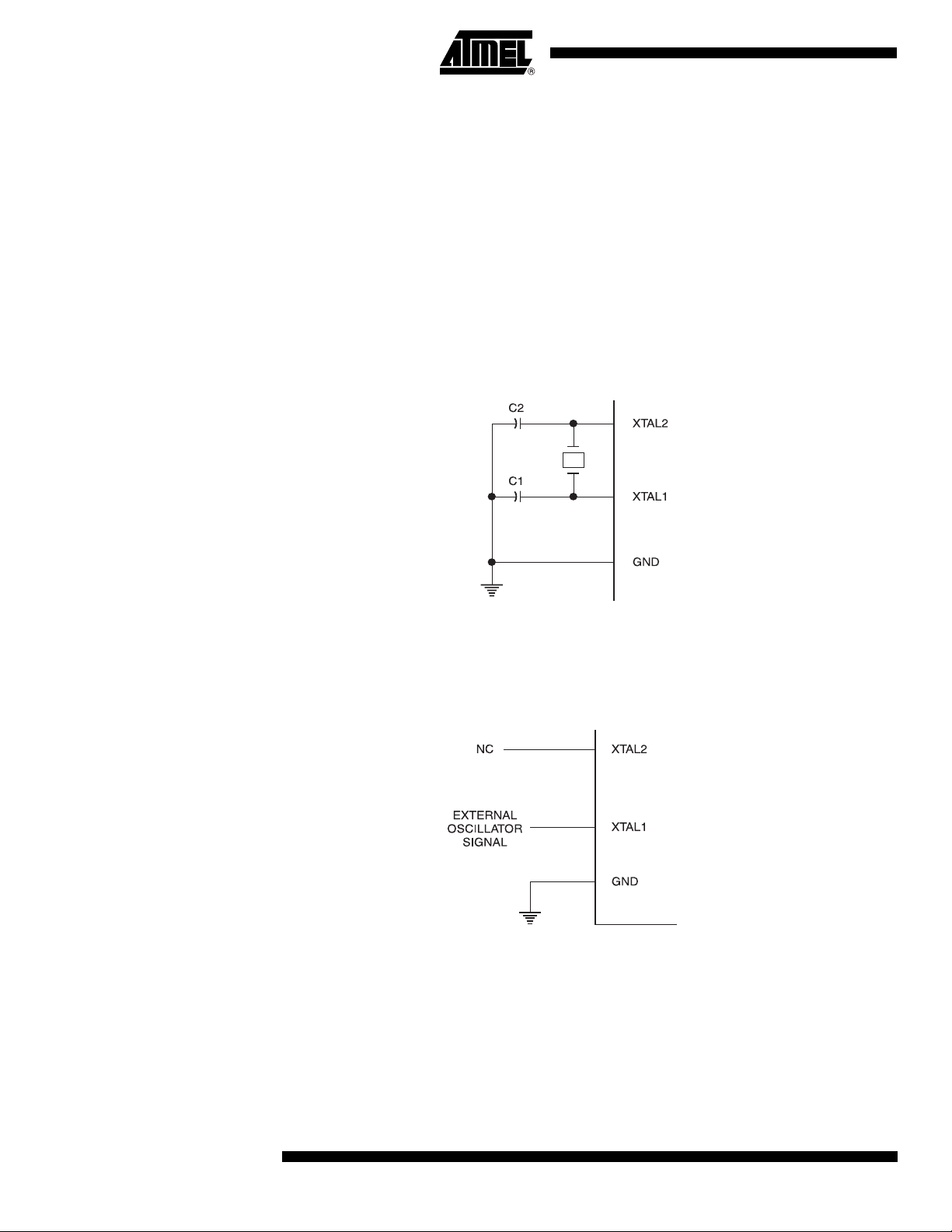
5. Oscillator Characteristics
XTAL1 and XTAL2 are the input and output, respectively, of an inverting amplifier which can be
configured for use as an on-chip oscillator, as shown in Figure 5-1. Either a quartz crystal or
ceramic resonator may be used. To drive the device from an external clock source, XTAL2
should be left unconnected while XTAL1 is driven as shown in Figure 5-2. There are no requirements on the duty cycle of the external clock signal, since the input to the internal clocking
circuitry is through a divide-by-two flip-flop, but minimum and maximum voltage high and low
time specifications must be observed.
Figure 5-1. Oscillator Connections
Note: C1, C2 = 30 pF ± 10 pF for Crystals
= 40 pF ± 10 pF for Ceramic Resonators
Figure 5-2. External Clock Drive Configuration
4
AT89C4051
1001E–MICRO–6/05

AT89C4051
6. Special Function Registers
A map of the on-chip memory area called the Special Function Register (SFR) space is shown in
the Table 6-1.
Note that not all of the addresses are occupied, and unoccupied addresses may not be implemented on the chip. Read accesses to these addresses will in general return random data, and
write accesses will have an indeterminate effect.
User software should not write 1s to these unlisted locations, since they may be used in future
products to invoke new features. In that case, the reset or inactive values of the new bits will
always be 0.
Table 6-1. AT89C4051 SFR Map and Reset Values
0F8H 0FFH
0F0H
0E8H 0EFH
0E0H
0D8H 0DFH
0D0H
0C8H
0C0H 0C7H
0B8H
0B0H
0A8H
0A0H
B
00000000
ACC
00000000
PSW
00000000
IP
XXX00000
P3
11111111
IE
0XX00000
0F7H
0E7H
0D7H
0CFH
0BFH
0B7H
0AFH
0A7H
98H
90H
88H
80H
1001E–MICRO–6/05
SCON
00000000
11111111
TCON
00000000
P1
SBUF
XXXXXXXX
TMOD
00000000
SP
00000111
TL0
00000000
DPL
00000000
TL1
00000000
DPH
00000000
TH0
00000000
TH1
00000000
PCON
0XXX0000
9FH
97H
8FH
87H
5

7. Restrictions on Certain Instructions
The AT89C4051 is an economical and cost-effective member of Atmel’s growing family of microcontrollers. It contains 4K bytes of Flash program memory. It is fully compatible with the MCS-51
architecture, and can be programmed using the MCS-51 instruction set. However, there are a
few considerations one must keep in mind when utilizing certain instructions to program this
device.
All the instructions related to jumping or branching should be restricted such that the destination
address falls within the physical program memory space of the device, which is 4K for the
AT89C4051. This should be the responsibility of the software programmer. For example, LJMP
0FE0H would be a valid instruction for the AT89C4051 (with 4K of memory), whereas LJMP
1000H would not.
7.1 Branching Instructions
LCALL, LJMP, ACALL, AJMP, SJMP, JMP @A+DPTR. These unconditional branching instruc-
tions will execute correctly as long as the programmer keeps in mind that the destination
branching address must fall within the physical boundaries of the program memory size (locations 00H to FFFH for the 89C4051). Violating the physical space limits may cause unknown
program behavior.
CJNE [...], DJNZ [...], JB, JNB, JC, JNC, JBC, JZ, JNZ. With these conditional branching
instructions the same rule above applies. Again, violating the memory boundaries may cause
erratic execution.
For applications involving interrupts, the normal interrupt service routine address locations of the
80C51 family architecture have been preserved.
7.2 MOVX-related Instructions, Data Memory
The AT89C4051 contains 128 bytes of internal data memory. Thus, in the AT89C4051 the stack
depth is limited to 128 bytes, the amount of available RAM. External DATA memory access is
not supported in this device, nor is external Program memory execution. Therefore, no MOVX
[...] instructions should be included in the program.
A typical 80C51 assembler will still assemble instructions, even if they are written in violation of
the restrictions mentioned above. It is the responsibility of the controller user to know the physical features and limitations of the device being used and adjust the instructions used
correspondingly.
8. Program Memory Lock Bits
On the chip are two lock bits which can be left unprogrammed (U) or can be programmed (P) to
obtain the additional features listed in the Table 8-1.
Table 8-1. Lock Bit Protection Modes
Program Lock Bits
1 U U No program lock features
(1)
Protection TypeLB1 LB2
2 P U Further programming of the Flash is disabled
3 P P Same as mode 2, also verify is disabled
Note: 1. The Lock Bits can only be erased with the Chip Erase operation.
6
AT89C4051
1001E–MICRO–6/05
9. Idle Mode
In idle mode, the CPU puts itself to sleep while all the on-chip peripherals remain active. The
mode is invoked by software. The content of the on-chip RAM and all the special functions registers remain unchanged during this mode. The idle mode can be terminated by any enabled
interrupt or by a hardware reset.
P1.0 and P1.1 should be set to “0” if no external pullups are used, or set to “1” if external
pullups are used.
It should be noted that when idle is terminated by a hardware reset, the device normally
resumes program execution, from where it left off, up to two machine cycles before the internal
reset algorithm takes control. On-chip hardware inhibits access to internal RAM in this event, but
access to the port pins is not inhibited. To eliminate the possibility of an unexpected write to a
port pin when Idle is terminated by reset, the instruction following the one that invokes Idle
should not be one that writes to a port pin or to external memory.
10. Power-down Mode
In the power-down mode the oscillator is stopped and the instruction that invokes power-down is
the last instruction executed. The on-chip RAM and Special Function Registers retain their values until the power-down mode is terminated. The only exit from power-down is a hardware
reset. Reset redefines the SFRs but does not change the on-chip RAM. The reset should not be
activated before V
enough to allow the oscillator to restart and stabilize.
AT89C4051
is restored to its normal operating level and must be held active long
CC
P1.0 and P1.1 should be set to “0” if no external pullups are used, or set to “1” if external
pullups are used.
11. Brown-out Detection
When VCC drops below the detection threshold, all port pins (except P1.0 and P1.1) are weakly
pulled high. When V
delay of typically 15 msec. The nominal brown-out detection threshold is 2.1V ± 10%.
goes back up again, an internal Reset is automatically generated after a
CC
V
CC
PORT PIN
INTERNAL RESET
2.1V
2.1V
15 msec.
1001E–MICRO–6/05
7

12. Programming The Flash
The AT89C4051 is shipped with the 4K bytes of on-chip PEROM code memory array in the
erased state (i.e., contents = FFH) and ready to be programmed. The code memory array is programmed one byte at a time. Once the array is programmed, to re-program any non-blank byte,
the entire memory array needs to be erased electrically.
Internal Address Counter: The AT89C4051 contains an internal PEROM address counter
which is always reset to 000H on the rising edge of RST and is advanced by applying a positive
going pulse to pin XTAL1.
Programming Algorithm: To program the AT89C4051, the following sequence is
recommended.
1. Power-up sequence:
Apply power between VCC
Set RST and XTAL1 to GND
2. Set pin RST to “H”
Set pin P3.2 to “H”
3. Apply the appropriate combination of “H” or “L” logic
levels to pins P3.3, P3.4, P3.5, P3.7 to select one of the programming operations
shown in the PEROM Programming Modes table.
To Program and Verify the Array:
4. Apply data for Code byte at location 000H to P1.0 to P1.7.
5. Raise RST to 12V to enable programming.
6. Pulse P3.2 once to program a byte in the PEROM array or the lock bits. The byte-write
cycle is self-timed and typically takes 1.2 ms.
7. To verify the programmed data, lower RST from 12V to logic “H” level and set pins P3.3
to P3.7 to the appropriate levels. Output data can be read at the port P1 pins.
8. To program a byte at the next address location, pulse XTAL1 pin once to advance the
internal address counter. Apply new data to the port P1 pins.
9. Repeat steps 6 through 8, changing data and advancing the address counter for the
entire 4K bytes array or until the end of the object file is reached.
10. Power-off sequence:
set XTAL1 to “L”
set RST to “L”
Tur n V
CC
Data
Polling: The AT89C4051 features Data Polling to indicate the end of a write cycle. During
a write cycle, an attempted read of the last byte written will result in the complement of the written data on P1.7. Once the write cycle has been completed, true data is valid on all outputs, and
the next cycle may begin. Data
power off
and GND pins
Polling may begin any time after a write cycle has been initiated.
Ready/Busy
signal. Pin P3.1 is pulled low after P3.2 goes High during programming to indicate BUSY. P3.1 is
pulled High again when programming is done to indicate READY.
8
AT89C4051
: The Progress of byte programming can also be monitored by the RDY/BSY output
1001E–MICRO–6/05

AT89C4051
Program Verify: If lock bits LB1 and LB2 have not been programmed code data can be read
back via the data lines for verification:
1. Reset the internal address counter to 000H by bringing RST from “L” to “H”.
2. Apply the appropriate control signals for Read Code data and read the output data at
the port P1 pins.
3. Pulse pin XTAL1 once to advance the internal address counter.
4. Read the next code data byte at the port P1 pins.
5. Repeat steps 3 and 4 until the entire array is read.
The lock bits cannot be verified directly. Verification of the lock bits is achieved by observing that
their features are enabled.
Chip Erase: The entire PEROM array (4K bytes) and the two Lock Bits are erased electrically
by using the proper combination of control signals and by holding P3.2 low for 10 ms. The code
array is written with all “1”s in the Chip Erase operation and must be executed before any nonblank memory byte can be re-programmed.
Reading the Signature Bytes: The signature bytes are read by the same procedure as a normal verification of locations 000H, 001H, and 002H, except that P3.5 and P3.7 must be pulled to
a logic low. The values returned are as follows.
(000H) = 1EH indicates manufactured by Atmel
(001H) = 41H indicates AT89C4051
13. Programming Interface
Every code byte in the Flash array can be written and the entire array can be erased by using
the appropriate combination of control signals. The write operation cycle is self-timed and once
initiated, will automatically time itself to completion.
Most major worldwide programming vendors offer support for the Atmel AT89 microcontroller
series. Please contact your local programming vendor for the appropriate software revision.
13.1 Flash Programming Modes
Mode RST/V
Write Code Data
Read Code Data
Write Lock
(1)(3)
(1)
Bit - 112V HHHH
Bit - 2 12V H H L L
PP
12V L H H H
HHLLHH
P3.2/PROG P3.3 P3.4 P3.5 P3.7
Chip Erase 12V H L L L
Read Signature Byte H H L L L L
Notes: 1. The internal PEROM address counter is reset to 000H on the rising edge of RST and is advanced by a positive pulse at
XTAL1 pin.
2. Chip Erase requires a 10-ms PROG
3. P3.1 is pulled Low during programming to indicate RDY/BSY
1001E–MICRO–6/05
pulse.
.
(2)
9

Figure 13-1. Programming the Flash Memory
AT89C4051
Figure 13-2. Verifying the Flash Memory
P3.1
AT89C4051
RDY/BSY
PP
10
AT89C4051
1001E–MICRO–6/05
AT89C4051
14. Flash Programming and Verification Characteristics
TA = 20°C to 30°C, VCC = 5.0 ± 10%
Symbol Parameter Min Max Units
V
PP
I
PP
t
DVGL
t
GHDX
t
EHSH
t
SHGL
t
GHSL
t
GLGH
t
ELQV
t
EHQZ
t
GHBL
t
WC
t
BHIH
t
IHIL
Note: 1. Only used in 12-volt programming mode.
Programming Enable Voltage 11.5 12.5 V
Programming Enable Current 250 µA
Data Setup to PROG Low 1.0 µs
Data Hold after PROG 1.0 µs
P3.4 (ENABLE) High to V
PP
1.0 µs
VPP Setup to PROG Low 10 µs
VPP Hold after PROG 10 µs
PROG Width 1 110 µs
ENABLE Low to Data Valid 1.0 µs
Data Float after ENABLE 01.0 µs
PROG High to BUSY Low 50 ns
Byte Write Cycle Time 2.0 ms
RDY/BSY\ to Increment Clock Delay 1.0 µs
Increment Clock High 200 ns
15. Flash Programming and Verification Waveforms
1001E–MICRO–6/05
11

16. Absolute Maximum Ratings*
Operating Temperature ................................. -55°C to +125°C
Storage Temperature..................................... -65°C to +150°C
Voltage on Any Pin
with Respect to Ground.....................................-1.0V to +7.0V
Maximum Operating Voltage ............................................ 6.6V
DC Output Current...................................................... 25.0 mA
*NOTICE: Stresses beyond those listed under “Absolute
Maximum Ratings” may cause permanent damage to the device. This is a stress rating only and
functional operation of the device at these or any
other conditions beyond those indicated in the
operational sections of this specification is not
implied. Exposure to absolute maximum rating
conditions for extended periods may affect device
reliability.
17. DC Characteristics
TA = -40°C to 85°C, VCC = 2.7V to 6.0V (unless otherwise noted)
Symbol Parameter Condition Min Max Units
V
IL
V
IH
V
IH1
V
OL
V
OH
I
IL
Input Low-voltage -0.5 0.2 V
Input High-voltage (Except XTAL1, RST) 0.2 V
Input High-voltage (XTAL1, RST) 0.7 V
Output Low-voltage
(Ports 1, 3)
(1)
= 20 mA, VCC = 5V
I
OL
I
= 10 mA, VCC = 2.7V
OL
+ 0.9 V
CC
CC
CC
V
CC
IOH = -80 µA, VCC = 5V ± 10% 2.4 V
Output High-voltage
(Ports 1, 3)
Logical 0 Input Current
(Ports 1, 3)
I
= -30 µA 0.75 V
OH
I
= -12 µA 0.9 V
OH
= 0.45V -50 µA
V
IN
CC
CC
- 0.1 V
CC
+ 0.5 V
+ 0.5 V
0.5 V
V
V
I
TL
I
LI
V
OS
V
CM
Logical 1 to 0 Transition Current
(Ports 1, 3)
Input Leakage Current
(Port P1.0, P1.1)
Comparator Input Offset Voltage VCC = 5V 20 mV
Comparator Input Common
Mode Voltage
V
= 2V, VCC = 5V ± 10% -750 µA
IN
0 < V
IN
< V
CC
0V
±10 µA
CC
RRST Reset Pulldown Resistor 50 300 KΩ
C
IO
I
CC
Pin Capacitance Test Freq. = 1 MHz, TA = 25°C 10 pF
Power Supply Current
Power-down Mode
(2)
Active Mode, 12 MHz, V
Idle Mode, 12 MHz, VCC = 6V/3V
P1.0 & P1.1 = 0V or V
VCC = 6V, P1.0 & P1.1 = 0V or V
V
= 3V, P1.0 & P1.1 = 0V or V
CC
= 6V/3V 15/5.5 mA
CC
5/1 mA
CC
CC
CC
20 µA
5µA
Notes: 1. Under steady state (non-transient) conditions, IOL must be externally limited as follows:
Maximum I
Maximum total I
exceeds the test condition, VOL may exceed the related specification. Pins are not guaranteed to sink current greater
If I
OL
per port pin: 20 mA
OL
for all output pins: 80 mA
OL
than the listed test conditions.
2. Minimum V
for Power-down is 2V.
CC
V
12
AT89C4051
1001E–MICRO–6/05

18. External Clock Drive Waveforms
19. External Clock Drive
Symbol Parameter
= 2.7V to 6.0V VCC = 4.0V to 6.0V
V
CC
AT89C4051
UnitsMin Max Min Max
1/t
t
CLCL
t
CHCX
t
CLCX
t
CLCH
t
CHCL
CLCL
Oscillator Frequency 0 12 0 24 MHz
Clock Period 83.3 41.6 ns
High Time 30 15 ns
Low Time 30 15 ns
Rise Time 20 20 ns
Fall Time 20 20 ns
1001E–MICRO–6/05
13

20. Serial Port Timing: Shift Register Mode Test Conditions
VCC = 5.0V ± 20%; Load Capacitance = 80 pF
12 MHz Osc Variable Oscillator
Symbol Parameter
UnitsMin Max Min Max
t
XLXL
t
QVXH
t
XHQX
t
XHDX
t
XHDV
Serial Port Clock Cycle Time 1.0 12t
Output Data Setup to Clock Rising Edge 700 10t
Output Data Hold after Clock Rising Edge 50 2t
Input Data Hold after Clock Rising Edge 0 0 ns
Clock Rising Edge to Input Data Valid 700 10t
21. Shift Register Mode Timing Waveforms
22. AC Testing Input/Output Waveforms
(1)
CLCL
-133 ns
CLCL
-117 ns
CLCL
-133 ns
CLCL
µs
Note: 1. AC Inputs during testing are driven at VCC - 0.5V for a logic 1 and 0.45V for a logic 0. Timing measurements are made at V
min. for a logic 1 and VIL max. for a logic 0.
23. Float Waveforms
Note: 1. For timing purposes, a port pin is no longer floating when a 100 mV change from load voltage occurs. A port pin begins to
float when 100 mV change from the loaded V
14
AT89C4051
(1)
OH/VOL
level occurs.
1001E–MICRO–6/05
IH
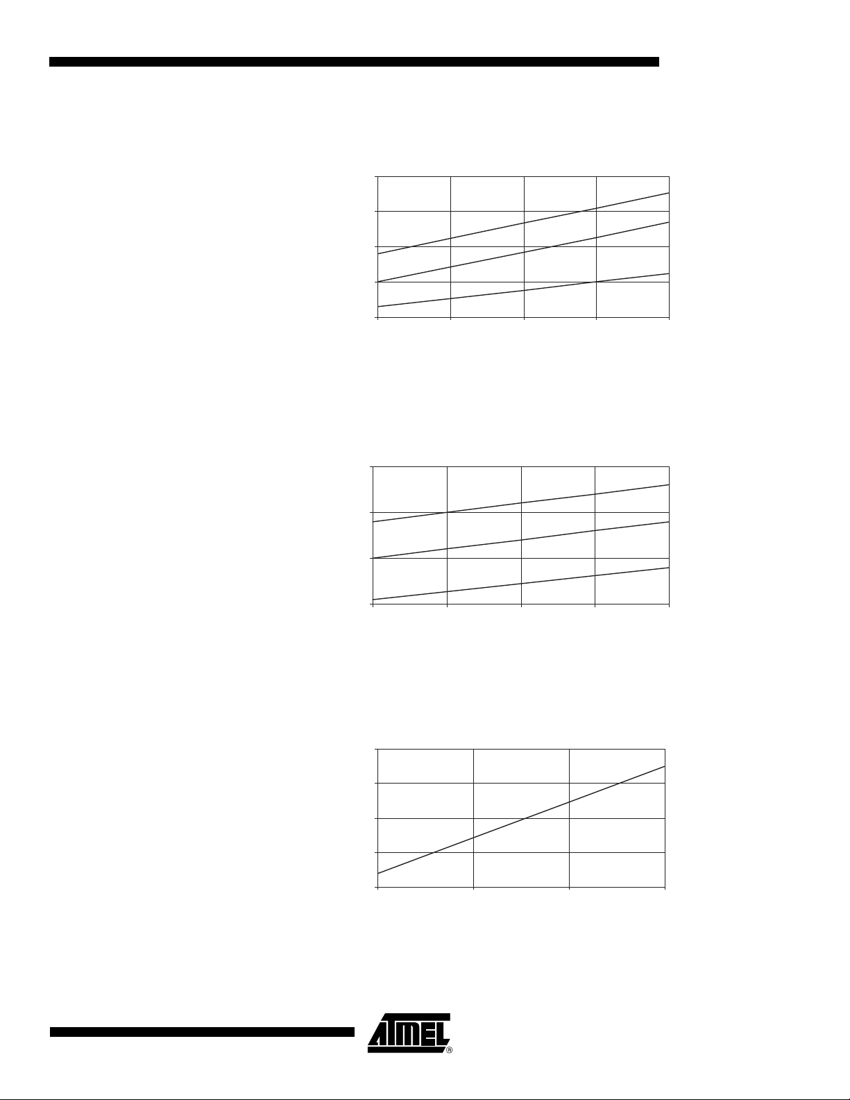
24. ICC (Active Mode) Measurements
20
15
I
C
C
10
m
5
A
0
AT89C4051
AT89C4051
TYPICAL ICC - ACTIVE (85˚C)
Vcc= 6.0V
Vcc= 5.0V
Vcc= 3.0V
0 6 12 18 24
FREQUENCY (MHz)
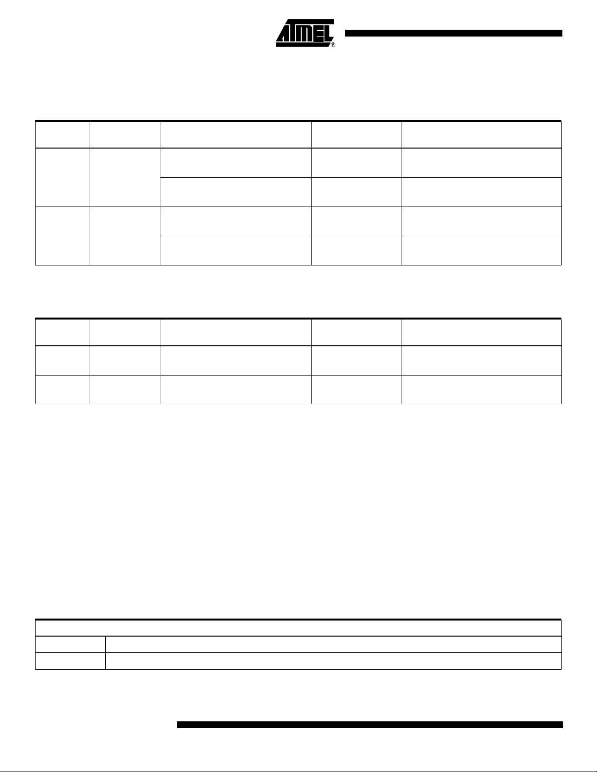
25. I
26. I
(Idle Mode) Measurements
CC
3
I
2
C
C
1
m
A
0
036912
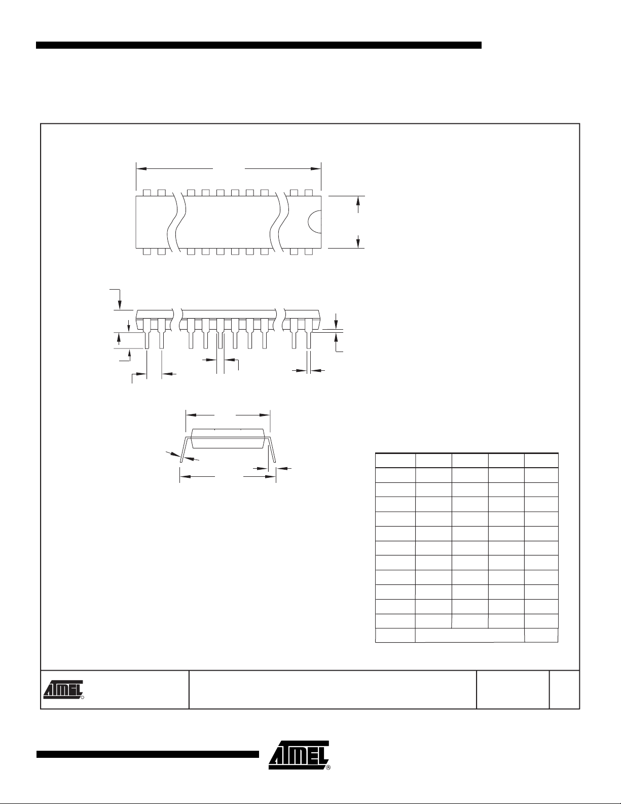
(Power Down Mode) Measurements
CC
TYPICAL ICC vs.VOLTAGE- POWER DOWN (85˚C)
20
15
I
C
C
10
AT89C4051
TYPICAL ICC - IDLE (85˚C)
Vcc= 6.0V
Vcc= 5.0V
Vcc= 3.0V
FREQUENCY (MHz)
AT89C4051
1001E–MICRO–6/05
µ
5
A
0
3.0V 4.0V 5.0V 6.0V
Notes: 1. XTAL1 tied to GND
2. P.1.0 and P1.1 = VCC or GND
3. Lock bits programmed
Vcc VOLTAGE
15
27. Ordering Information
27.1 Standard Package
Speed
(MHz)
12 2.7V to 6.0V
24 4.0V to 6.0V
Power
Supply Ordering Code Package Operation Range
AT89C4051-12PC
AT89C4051-12SC
AT89C4051-12PI
AT89C4051-12SI
AT89C4051-24PC
AT89C4051-24SC
AT89C4051-24PI
AT89C4051-24SI
27.2 Green Package Option (Pb/Halide-free)
Speed
(MHz)
12 2.7V to 6.0V
24 4.0V to 6.0V
Power
Supply
Ordering Code Package Operation Range
AT89C4051-12PU
AT89C4051-12SU
AT89C4051-24PU
AT89C4051-24SU
20P3
20S
20P3
20S
20P3
20S
20P3
20S
20P3
20S
20P3
20S
Commercial
(0°C to 70°C)
Industrial
(-40°C to 85°C)
Commercial
(0°C to 70°C)
Industrial
(-40°C to 85°C)
Industrial
(-40°C to 85°C)
Industrial
(-40°C to 85°C)
Package Type
20P3 20-lead, 0.300” Wide, Plastic Dual In-line Package (PDIP)
20S 20-lead, 0.300” Wide, Plastic Gull Wing Small Outline (SOIC)
16
AT89C4051
1001E–MICRO–6/05
28. Package Information
PIN
1
E1
A1
B
E
B1
C
L
SEATING PLANE
A
28.1 20P3 – PDIP
AT89C4051
D
e
eC
eB
Notes: 1. This package conforms to JEDEC reference MS-001, Variation AD.
2. Dimensions D and E1 do not include mold Flash or Protrusion.
Mold Flash or Protrusion shall not exceed 0.25 mm (0.010").
2325 Orchard Parkway
R
San Jose, CA 95131
TITLE
20P3, 20-lead (0.300"/7.62 mm Wide) Plastic Dual
Inline Package (PDIP)
COMMON DIMENSIONS
(Unit of Measure = mm)
SYMBOL
A – – 5.334
A1 0.381 – –
D 24.892 – 26.924 Note 2
E 7.620 – 8.255
E1 6.096 – 7.112 Note 2
B 0.356 – 0.559
B1 1.270 – 1.551
L 2.921 – 3.810
C 0.203 – 0.356
eB – – 10.922
eC 0.000 – 1.524
e 2.540 TYP
MIN
NOM
MAX
DRAWING NO.
20P3
NOTE
1/23/04
REV.
D
1001E–MICRO–6/05
17

28.2 20S – SOIC
Dimensions in Millimeters and (Inches).
Controlling dimension: Inches.
JEDEC Standard MS-013
0.51(0.020)
0.33(0.013)
PIN 1 ID
PIN 1
1.27 (0.050) BSC
13.00 (0.5118)
12.60 (0.4961)
0.30(0.0118)
0.10 (0.0040)
7.60 (0.2992)
7.40 (0.2914)
2.65 (0.1043)
2.35 (0.0926)
10.65 (0.419)
10.00 (0.394)
18
2325 Orchard Parkway
R
San Jose, CA 95131
AT89C4051
0º ~ 8º
1.27 (0.050)
0.40 (0.016)
0.32 (0.0125)
0.23 (0.0091)
TITLE
20S, 20-lead, 0.300" Body, Plastic Gull Wing Small Outline (SOIC)
DRAWING NO.
20S
1001E–MICRO–6/05
10/23/03
REV.
B
 Loading...