

ATMEL AT89C2051 User Manual
Features
http://www.BDTIC.com/ATMEL
•
Compatible with MCS-51™ Products
•
2K Bytes of Reprogrammable Flash Memory
– Endurance: 1,000 Write/Erase Cycles
•
2.7V to 6V Operating Range
•
Fully Static Operation: 0 Hz to 24 MHz
•
T wo-Level Pro gr am Me mory Loc k
•
128 x 8-Bit Internal RAM
•
15 Programmable I/O Lines
•
Two 16-Bit Timer/Counters
•
Six Interrupt Sources
•
Programmable Serial UART Channel
•
Direct LED Drive Outputs
•
On-Chip Analog Comparator
•
Low Power Idle and Power Down Modes
8-Bit
Microcontroller
with 2K Bytes
Description
The AT89C2051 is a low-vo ltage, high-pe rformanc e CMOS 8 -bit micr ocompu ter with
2K Bytes of Flash programmable and erasa ble read only memory (PERO M). The
device is manufactured using Atmel’s high density nonvolatile memory technology
and is compatibl e with the in dustry standard MCS-51™ instru ctio n set. By comb ining
a versatile 8-bit CPU with Flash on a monolithic chip, the Atmel AT89C2051 is a powerful microcomputer which provides a highly flexible and c ost effective solutio n to
many embedded control applications.
The AT89C2051 provides the following standard features: 2K Bytes of Flash, 128
bytes of RAM, 15 I/O lines, two 16-b it time r/cou nters, a five vect or two- level i nterru pt
architecture, a full duplex serial port, a precision analog comparator, on-chip oscillator
and clock circuitry. In a ddi tio n, the AT89C2051 is designe d wi th sta t ic l og ic for oper a tion down to zero frequency and supports two software selectable power saving
modes. The Idle Mode stops the CPU while allowing the RAM, timer/counters, serial
port and interrupt system to continue functioning. The Power Down Mode saves the
RAM contents but freezes the oscillator disabling all other chip functions until the next
hardware reset.
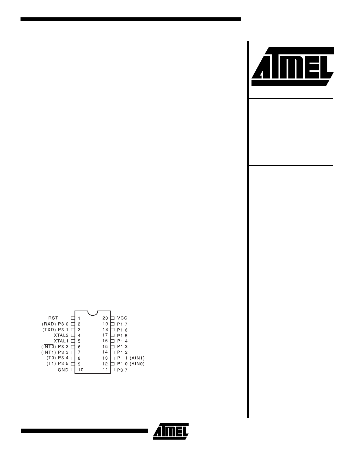
Pin Configuration
PDIP/SOIC
/VPP
Flash
AT89C2051
0368D-B–12/97
4-15
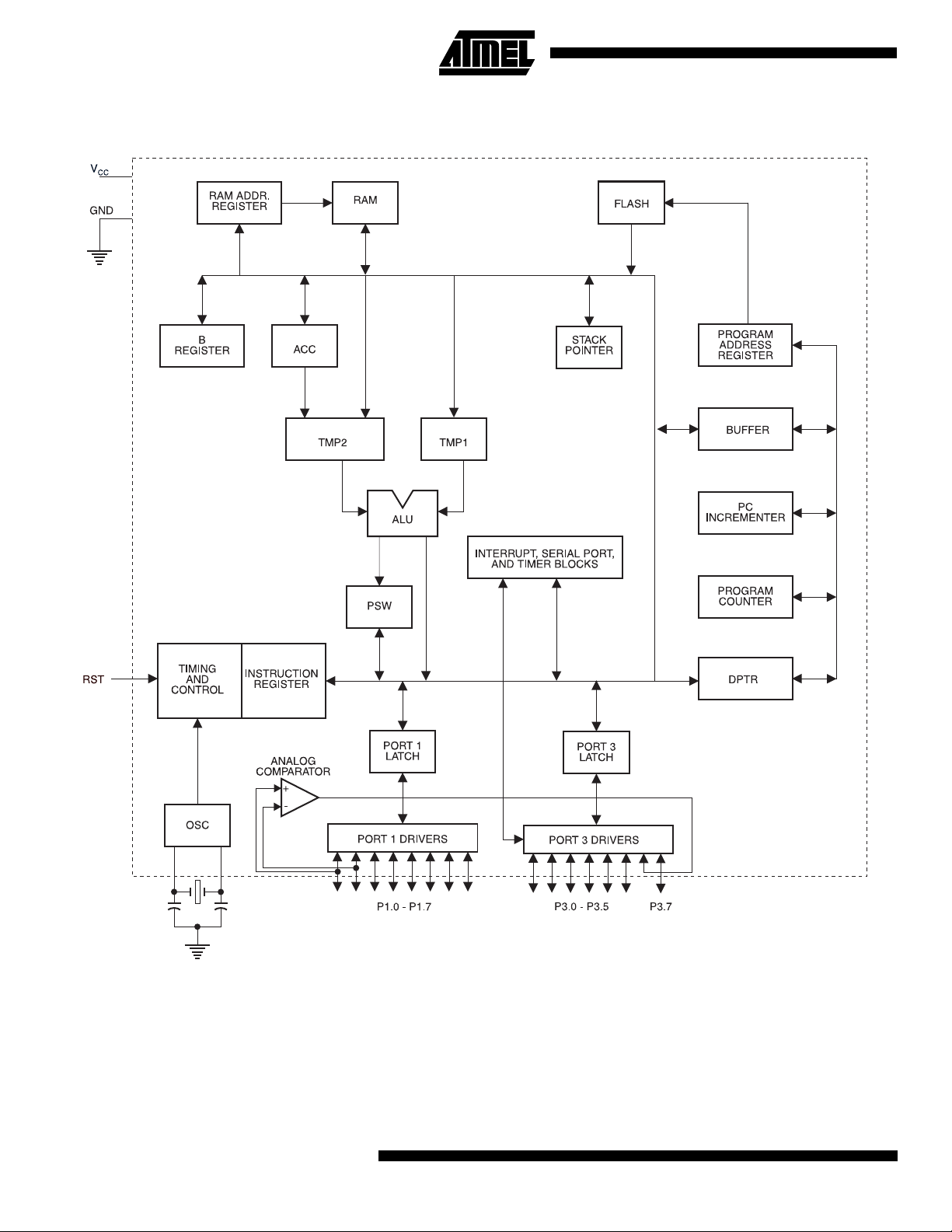
Block Diagram
http://www.BDTIC.com/ATMEL
4-16
AT89C2051
AT89C2051
http://www.BDTIC.com/ATMEL
Pin Description
V
CC
Supply voltage.
GND
Ground.
Port 1
Port 1 is an 8-bit bidirectional I/O port. Port pins P1.2 to
P1.7 provide interna l pullup s. P1. 0 and P1 .1 requ ire ext ernal pullups. P1.0 and P1.1 also serve as the positive input
(AIN0) and the negativ e input (AIN1), res pectively, of the
on-chip precision analog comparator. The Port 1 output
buffers can sink 20 mA and can drive LED displays directly.
When 1s are written to Port 1 pins, they can be used as
inputs. When pins P 1.2 to P1.7 ar e used a s inp uts an d are
externally pulled low, they will source current (I
of the internal pullups.
Port 1 also receives code data during Flash programming
and verification.
Port 3
Port 3 pins P3.0 to P3 .5, P3.7 are sev en bidirecti onal I/O
pins with inter nal pullups . P 3.6 i s har d-wire d as an input to
the output of the on-chip comparator and is not accessible
as a general purpose I/O pin. The Port 3 output buffers can
sink 20 mA. When 1s are writt en to Port 3 pins they are
pulled high by th e internal pullup s and can be use d as
inputs. As inputs, Port 3 pins that are externally being
pulled low will source current (I
Port 3 also se rves the fu nctio ns o f vari ous sp ecial feat ures
of the AT89C2051 as listed below:
) because of the pullups.
IL
) because
IL
XTAL2
Output from the inverting oscillator amplifier.
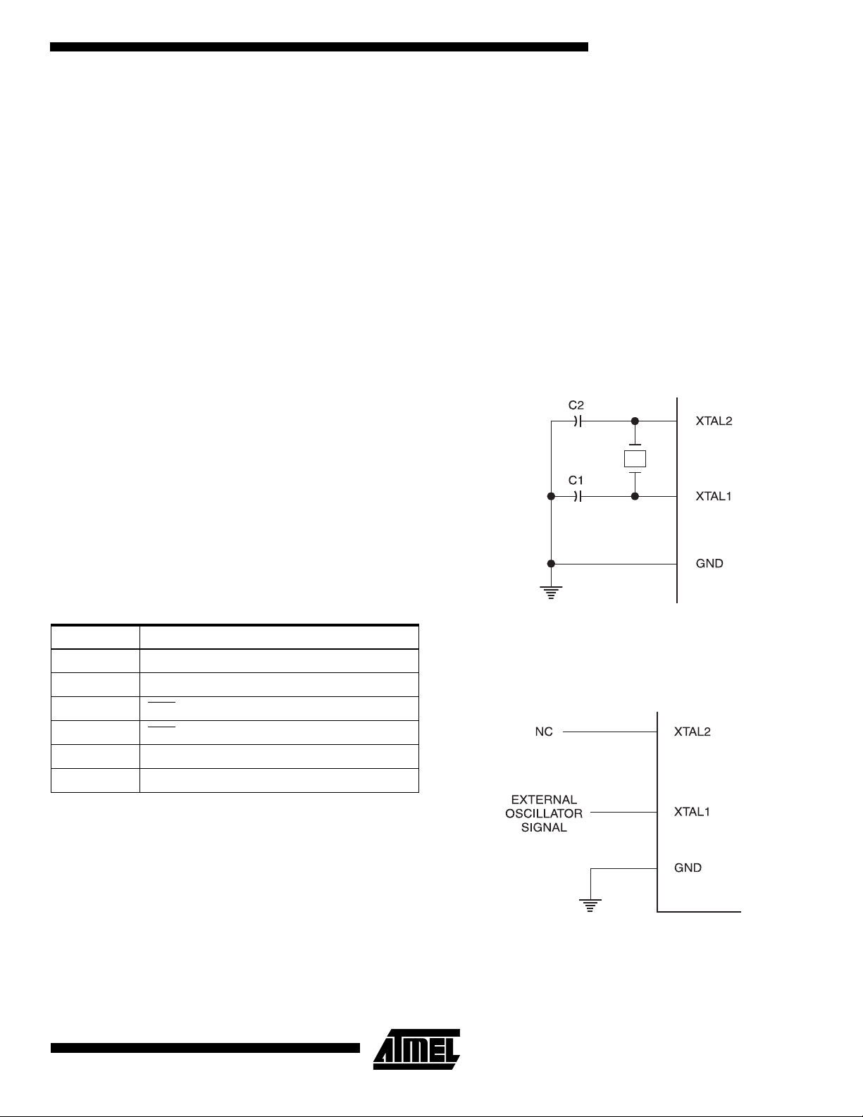
Oscillator Characteristics
XTAL1 and XTAL2 are the input and output, respecti vely,
of an inverting amplif ier which can be con figured for use as
an on-chip oscillator, as shown in Figure 1. Either a quartz
crystal or ceramic resonator may be used. To drive the
device from an external clock source, XTAL2 should be left
unconnected while XTAL1 is driven as shown in Fi gure 2.
There are no requirements on the duty cycle of the external
clock signal, since the input to the internal clocking circuitry
is through a divide-by-two flip-flop, but minimum and maximum voltage high and low tim e specificat ions must be
observed.
Figure 1.
Oscillator Connections
Port Pin Alternate Functions
P3.0 RXD (serial input port)
P3.1 TXD (serial output port)
P3.2 INT0 (external interrupt 0)
P3.3 INT1
P3.4 T0 (timer 0 external input)
P3.5 T1 (timer 1 external input)
Port 3 also receives some control signals for Flash programming and verification.
RST
Reset input. All I/O pins are reset to 1s as soon as RST
goes high. Holding the RST pin high for two machine cycles
while the oscillator is running resets the device.
Each machine cycle takes 12 oscillator or clock cycles.
XTAL1
Input to the inverting os cillator ampl ifier and input to the
internal clock operating circuit.
(external interrupt 1)
Note: C1, C2 = 30 pF ± 10 pF for Cry s tals
= 40 pF ± 10 pF for Ceramic Resonators
Figure 2.
External Clock Drive Configuration
4-17

Special Function Registers
http://www.BDTIC.com/ATMEL
A map of the on-chip memory area called the Special Function Register (SFR) space is shown in the table below.
Note that not all of the addresses are occupied, and unoccupied addresses may not be implemented on the chip.
Read accesses to these addresses will in general return
random data, and write accesses will have an indeterminate effect.
User software should not write 1s to these unlisted locations, since they may be used in future products to invoke
new features. In th at case, th e reset or inac tive valu es of
the new bits will always be 0.
Table 1.
0F8H 0FFH
0F0H B
0E8H 0EFH
0E0H ACC
0D8H 0DFH
0D0H PSW
0C8H 0CFH
0C0H 0C7H
0B8H IP
0B0H P3
AT89C2051 SFR Map and Reset Values
0F7H
00000000
0E7H
00000000
0D7H
00000000
0BFH
XXX00000
0B7H
11111111
0A8H IE
0XX00000
0A0H 0A7H
98H SCON
00000000
90H P1
11111111
88H TCON
00000000
80H SP
4-18
SBUF
XXXXXXXX
TMOD
00000000
00000111
TL0
00000000
DPL
00000000
AT89C2051
TL1
00000000
DPH
00000000
TH0
00000000
TH1
00000000
PCON
0XXX0000
0AFH
9FH
97H
8FH
87H
 Loading...