

Page 1

BDTIC www.BDTIC.com/ATMEL
Features
• 80C51 Compatible CPU Core High-speed Architecture
• X2 Speed Improvement Capability (6 Clocks/Machine Cycle)
• 16 MHz in Standard or X2 mode
• 256 Bytes RAM
• 256 Bytes XRAM
• 12K Bytes ROM/OTP Program Memory
• Two 16-bit Timer/Counters T0, T1
• 5 Channels Programmable Counter Array with High-speed Output, Compare/Capture,
Pulse Width Modulation and Watchdog Timer Capabilities
• SPI Interface (Master and Slave mode)
• Interrupt Structure with:
– 6 Interrupt Sources
– 4 Interrupt Priority Levels
• Power Supply: 3 - 5.5V
• Temperature Range: Industrial (-40
• Package: SSOP16, SSOP24
o
C to 85oC), Automotive (-40oC to 125oC)
Low-pin Count
8-bit
Microcontroller
Description
The AT8xC5103 is a high-performance ROM/OTP version of the 80C51 8-bit Microcontroller in 16 and 24-pin packages.
The AT8xC5103 contains a standard C51 CPU core with 12 Kbytes ROM/OTP program memory, 256 bytes of internal RAM, 256 bytes of extended internal RAM, a 5sources 4-level interrupt system, two timer/counters and a SPI serial bus controller.
The AT8xC5103 is also dedicated for analog interfacing applications. For this, it has a
five channels Programmable Counter Array.
In addition, the AT8xC5103 implements the X2 speed improvement mechanism. The
X2 feature allows to keep the same C PU power at a divided by two oscillator
frequency.
The fully static design of the AT8xC5103 allows to reduce system power consumption
by bringing the clock frequency down to any value, even DC, without loss of data.
AT87C5103
AT83C5103
Rev. 4134D–8051–02/08
1
Page 2
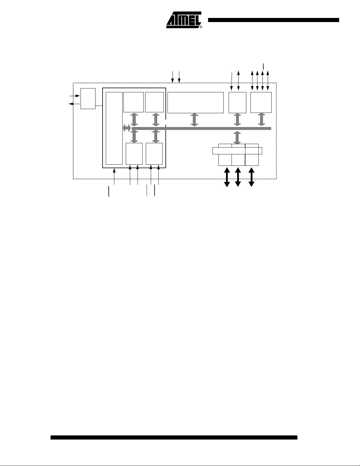
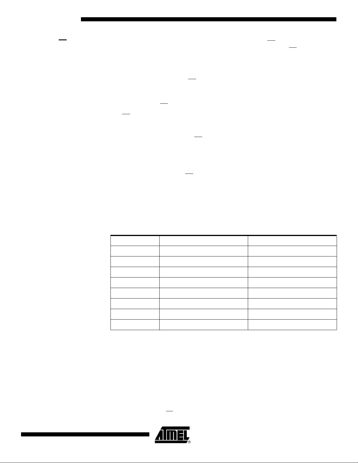
Block Diagram
Timer 0
INT
RAM
256x8
T0
XTAL2
XTAL1
CPU
Timer 1
Ctrl
INT0
C51
CORE
(3) (3)
Port 1
P1
P3
IB-bus
Vss
Vcc
ROM
12 K *8
CEX0-4
Xtal
Osc
(1)
Port 3
PCA
MISO
(1)
MOSI
(1)
SPSCK
(3)
SPI
SS
(1)
RST
ECI
(1)
256x8
Parallel I/O Ports
EXRAM
P4
Port 4
INT1
(3)
T1
(3)
Notes: 1. Alternate function of Port 1.
2. Alternate function of Port 3.
2
4134D–8051–02/08
Page 3
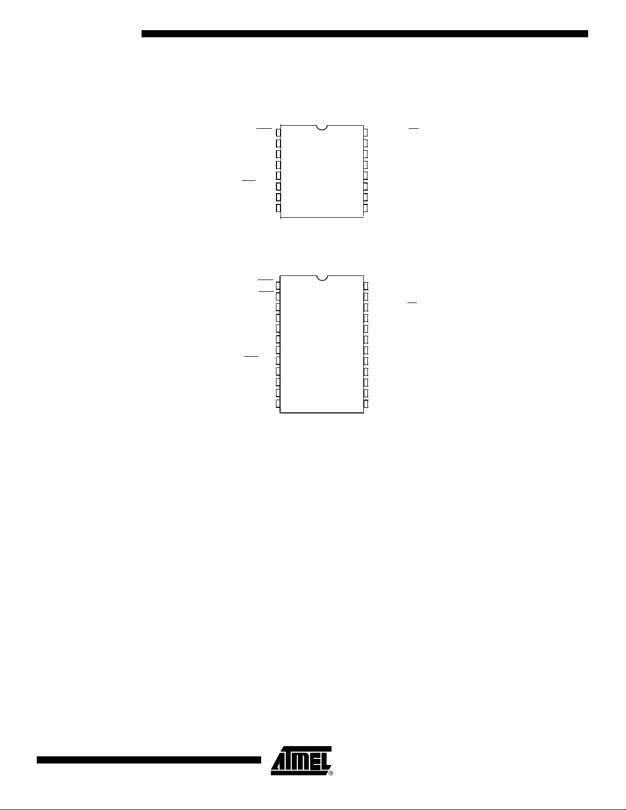
Pin Configurations
XTAL1
VCC
VSS
1
RST/VPP
XTAL2
P1.2/ECI/DIG2
P3.2/DIG0/INT0
P3.6/SPICK
P3.4/DIG1/T0
P1.7/CEX4/SS
P1.6/CEX3
P1.5/CEX2
P1.4/CEX1
P1.3/CEX0
2
3
4
5
6
7
8
16
15
14
13
12
11
10
9
P1.1/MOSI
P1.0/MISO
SSOP16
P1.1/MOSI
P1.0/MISO
VCC
XTAL2
P1.5/CEX2
VSS
XTAL1
P1.2/ECI/DIG2
RST/VPP
P3.1
P3.6/SPICK
1
2
3
4
5
6
7
8
16
15
14
13
9
10
11
12
P1.6/CEX3
P3.7
P3.5/T1
20
19
18
17
24
23
22
21
P3.4/DIG1/T0
P4.0
P4.1
P4.2
P1.3/CEX0
P1.4/CEX1
P3.0
P1.7/CEX4/SS
P3.3/INT1
P3.2/DIG0/INT0
SSOP24
4134D–8051–02/08
3
Page 4
Pin Description
Mnemonic Type Name and Function
V
SS
V
CC
P1.0 - P1.7
I Ground: 0V reference
I Power Supply: 3.0V or 5.5V
Port 1: Port 1 is an 8-bit programmable I/O port with internal pull-up
I/O
Alternate functions for Port 1 include:
I/O MISO (P1.0): Master IN, Slave OUT of the SPI controller
I/O MOSI (P1.1): Master OUT, Slave IN of the SPI controller
DIG2 (P1.2): Programmable as Output with Push-pull
I/O
ECI: External Clock for PCA
I/O CEX0 (P1.3): Capture/Compare External I/O for PCA module 0
I/O CEX1 (P1.4): Capture/Compare External I/O for PCA module 1
I/O CEX2 (P1.5): Capture/Compare External I/O for PCA module 2
I/O CEX3 (P1.6): Capture/Compare External I/O for PCA module 3
SS (P1.7): Slave select input of the SPI controller
I/O
CEX4: Capture/Compare External I/O for PCA module 3
XTAL1 I Input to the inverting oscillator amplifier
XTAL2 O Output from the inverting oscillator amplifier
RST/VPP
RST: Negative Reset input
A low on this pin for two machine cycles while the oscillator is running,
resets the device.
I
This pin will include a pull-down to reset the circuit if no external reset
level is applied.
VPP: High voltage input for OTP programming
P3.0 - P3.7 I/O Port 3: Port 3 is a 8-bit programmable I/O port with internal pull-up.
I/O P3.0: Programmable as Output with Push-pull.
I/O P3.1: Programmable as Output with Push-pull.
DIG0 (P3.2): Programmable as Output with Push-pull.
I/O
INT0: External Interrupt 0
P3.3: Programmable as Output with Push-pull.
I/O
INT1: External Interrupt 1
DIG1 (P3.4): Programmable as Output with Push-pull.
I/O
T0: Timer 0 external Input
P3.5: Programmable as Output with Push-pull.
I/O
T1: Timer 1 external Input
I/O SPICK (P3.6): Clock I/O of the SPI controller
I/O P3.7: Programmable as Output with Push-pull.
P4.0-P4.2 I/O
Port 4: Port 4 is an 3-bit I/O port with internal pull-up
4
4134D–8051–02/08
Page 5

Clock
The Errata Sheet core needs only 6 clock periods per machine cycle. This feature,
called ”X2”, provides the following advantages:
• Divides frequency crystals by 2 (cheaper crystals) while keeping the same CPU
power.
• Saves power consumption while keeping the same CPU power (oscillator power
saving).
• Saves power consumption by dividing dynamic operating frequency by 2 in
operating and idle modes.
• Increases CPU power by 2 while keeping the same crystal frequency.
In order to keep the original C51 compatibility, a divider-by-2 is inserted between the
XTAL1 signal and the main clock input of the core (phase generator). This divider may
be disabled by the software.
Description
The clock for the whole circuit and peripheral is first divided by 2 before being used by
the CPU core and peripherals. This allows any cyclic ratio to be accepted on the XTAL1
input. In X2 Mode, as this divider is bypassed, the signals on XTAL1 must have a cyclic
ratio between 40 to 60%. Figure 1. shows the clock generation block diagram. The X2
bit is validated on the XTAL1 ÷ 2 rising edge to avoid glitches when switching from the
X2 to the STD mode. Figure 2 shows the mode switching waveforms.
4134D–8051–02/08
5
Page 6
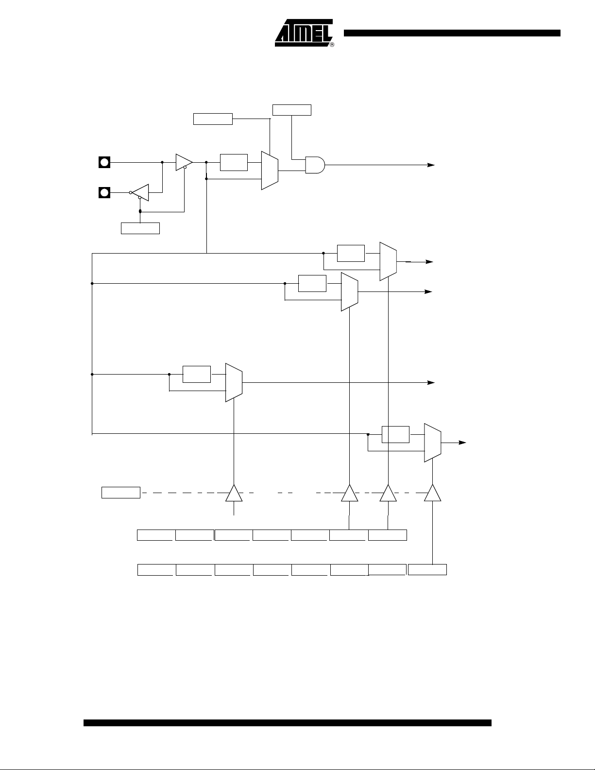
Figure 1. Clock CPU Generation Diagram
XTAL1
XTAL2
PD
PCON.1
1
0
÷
2
FCLK_PERIPH
Peripheral
X2
CKCON.0
CKCON0.7 CKCON0.6
PCAX2
CKCON0.5 CKCON0.4 CKCON0.3
T1X2
CKCON0.2
T0X2
CKCON0.1
IDL
PCON.0
1
0
÷
2
1
0
÷
2
1
0
÷
2
1
0
÷
2
X2
CKCON0.0
FSPI Clock
FPCA Clock
FT1 Clock
FT0 Clock
FCPU
CKCON1.7 CKCON1.6
CKCON1.5
CKCON1.4 CKCON1.3 CKCON1.2
CKCON1.1
SPIX2
CKCON1.0
Clock Symbol
6
4134D–8051–02/08
Page 7
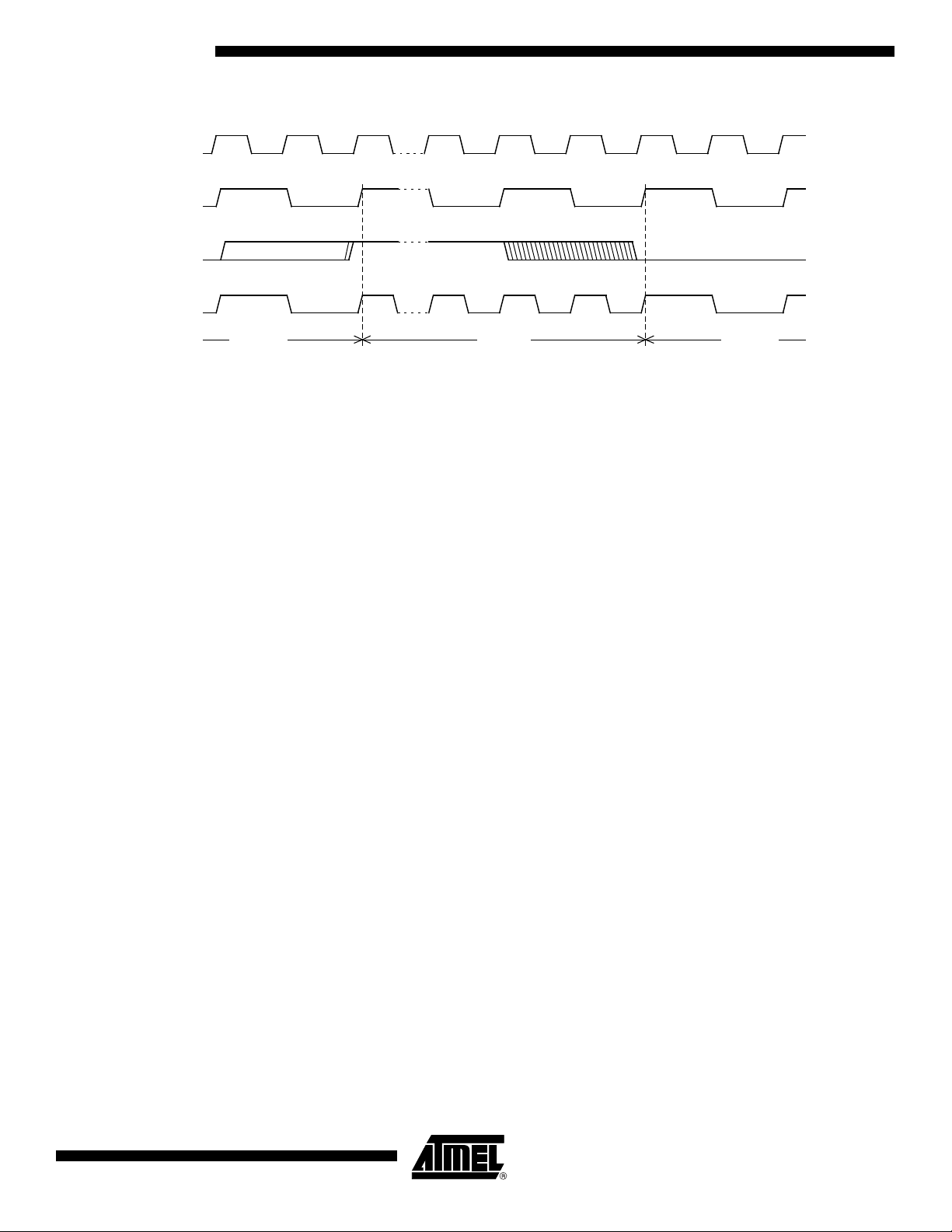
Figure 2. Mode Switching Waveforms
XTAL2
XTAL1
CPU Clock
X2 Bit
X2 ModeSTD Mode STD Mode
The X2 bit in the CKCON register (See Table 1) allows switching from 12 clock cycles
per instruction to 6 clock cycles and vice versa. At reset, the standard speed is activated
(STD mode). Setting this bit activates the X2 feature (X2 Mode).
Note: In order to prevent any incorrect operation while operating in the X2 Mode, users must be
aware that all peripherals using the clock frequency as a time reference (timers, PCA,
SPI) will have their time reference divided by 2. For example, a free running timer generating an interrupt every 20 ms will then generate an interrupt every 10 ms.
4134D–8051–02/08
7
Page 8

Registers
Table 1. CKCON0 Register
CKCON0 (S:8Fh)
Clock Control Register
7 6 5 4 3 2 1 0
PCAX2 T1X2 T0X2 X2
Bit
Number
7 –
6 –
5 PCAX2
4 –
3 –
2 T1X2
1 T0X2
0 X2
Bit
Mnemonic Description
Reserved
The value read from this bit is indeterminate. Do not set this bit.
Reserved
The value read from this bit is indeterminate. Do not set this bit.
Programmable Counter Array clock
Clear to select 6 clock periods per peripheral clock cycle.
Set to select 12 clock periods per peripheral clock cycle.
Reserved
The value read from this bit is indeterminate. Do not set this bit.
Reserved
The value read from this bit is indeterminate. Do not set this bit.
Timer1 Clock
Clear to select 6 clock periods per peripheral clock cycle.
Set to select 12 clock periods per peripheral clock cycle.
Timer0 Clock
Clear to select 6 clock periods per peripheral clock cycle.
Set to select 12 clock periods per peripheral clock cycle.
CPU Clock
Clear to select 12 clock periods per machine cycle (STD mode) for CPU and all
the peripherals.
Set to select 6 clock periods per machine cycle (X2 Mode) and to enable the
individual peripherals "X2" bits.
(1)
(1)
(1)
Note: 1. This control bit is validated when the CPU clock bit X2 is set; when X2 is low, this bit
has no effect.
Reset Value = XX0X X000b
8
4134D–8051–02/08
Page 9
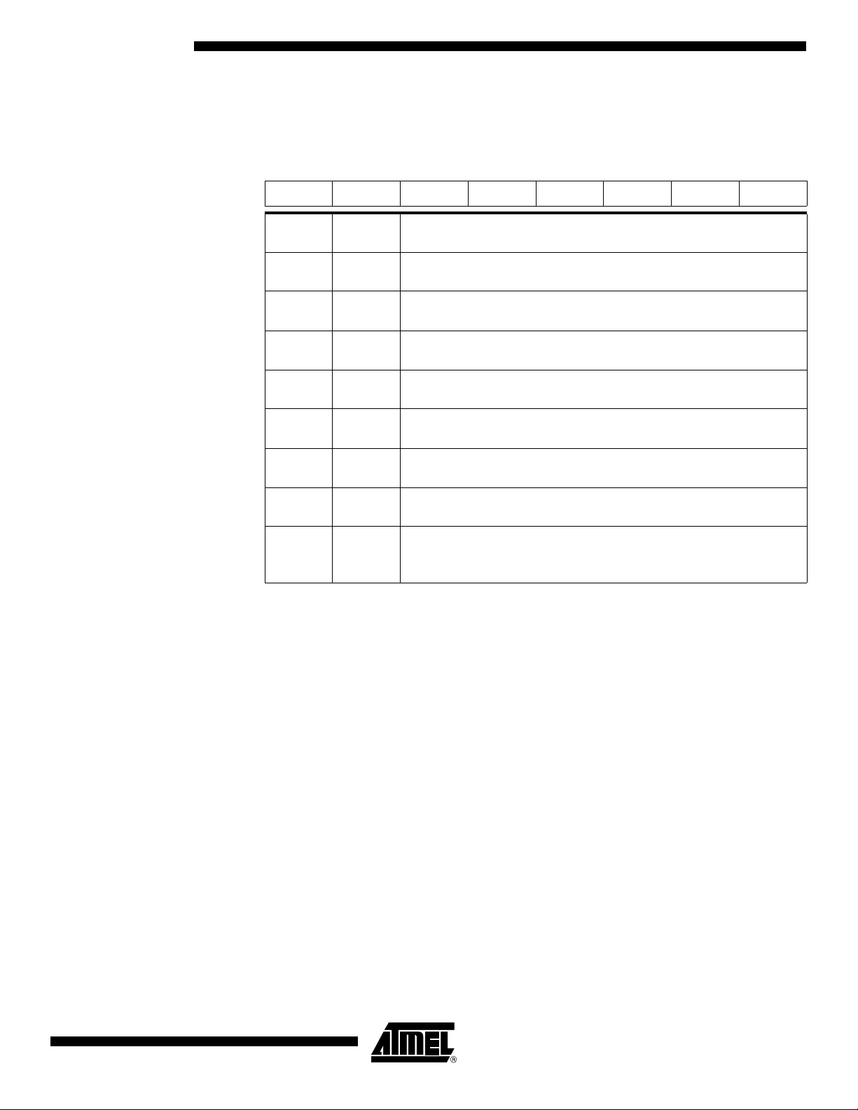
Table 2. CKCON1 Register
CKCON1 (S:AFh)
Clock Control Register
7 6 5 4 3 2 1 0
SPIX2
Bit
Number
7 –
6 –
5 –
4 –
3 –
2 –
1 –
0 SPIX2
Bit
Mnemonic Description
Reserved
The value read from this bit is indeterminate. Do not set this bit.
Reserved
The value read from this bit is indeterminate. Do not set this bit.
Reserved
The value read from this bit is indeterminate. Do not set this bit.
Reserved
The value read from this bit is indeterminate. Do not set this bit.
Reserved
The value read from this bit is indeterminate. Do not set this bit.
Reserved
The value read from this bit is indeterminate. Do not set this bit.
Reserved
The value read from this bit is indeterminate. Do not set this bit.
SPI clock
Clear to select 6 clock periods per peripheral clock cycle.
Set to select 12 clock periods per peripheral clock cycle.
(1)
Note: 1. This control bit is validated when the CPU clock bit X2 is set; when X2 is low, this bit
has no effect.
Reset Value = XXXX XXX0b
4134D–8051–02/08
9
Page 10

SFR Mapping
The Special Function Registers (SFRs) of the AT8xC5103 belong to the following
categories:
• C51 core registers: ACC, B, DPH, DPL, PSW, SP, AUXR1
• I/O port registers: P1, P3, P4, P1M1, P1M2, P3M1, P3M2
• Timer registers: TCON, TH0, TH1, TMOD, TL0, TL1
• Power and clock control registers: CKCON0, CKCON1, PCON
• Interrupt system registers: IE, IE1, IPL0, IPL1, IPH0, IPH1
• SPI: SPCON, SPSTA, SPDAT
• PCA: CCAP0L, CCAP1L, CCAP2L, CCAP3L, CCAP4L, CCAP0H, CCAP1H,
CCAP2H, CCAP3H, CCAP4H, CCAPM0, CCAPM1, CCAPM2, CCAPM3,
CCAPM4, CL, CH, CMOD, CCON
10
4134D–8051–02/08
Page 11
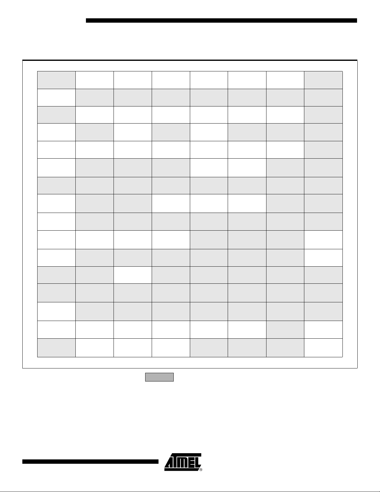
Table 3. SFR Addresses and Reset Values
0/8 1/9 2/A 3/B 4/C 5/D 6/E 7/F
F8h
F0h
E8h
E0h
D8h
D0h
C8h
C0h
B8h
B0h
A8h
B
0000 0000
ACC
0000 0000
CCON
00X0 0000
PSW
0000 0000
P4
XXXX X111
IPL0
X0XX 0000
P3
1111 1111
IE0
00XX 0000
CH
0000 0000
CL
0000 0000
CMOD
00XX X000
IE1
XXXX X0XX
CCAP0H
0000 0000
CCAP0L
0000 0000
P1M2
0000 0000
CCAPM0
X000 0000
IPL1
XXXX X0XX
CCAP1H
0000 0000
CCAP1L
0000 0000
CCAPM1
X000 0000
SPCON
0001 0100
IPH1
XXXX X0XX
CCAP2H
0000 0000
CCAP2L
0000 0000
P3M2
0000 0000
CCAPM2
X000 0000
P1M1
0000 0000
SPSTA
00X0 XXXX
CCAP3H
0000 0000
CCAP3L
0000 0000
CCAPM3
X000 0000
P3M1
0000 0000
SPDAT
XXXX XXXX
CCAP4H
0000 0000
CCAP4L
0000 0000
CCAPM4
X000 0000
IPH0
X0XX 0000
CKCON1
XXXX XXX0
FFh
F7h
EFh
E7h
DF
h
D7h
CF
h
C7h
BFh
B7h
AFh
A0h
98h 9Fh
90h
88h
80h
P1
1111 1111
TCON
0000 0000
0/8 1/9 2/A 3/B 4/C 5/D 6/E 7/F
TMOD
0000 0000
SP
0000 0111
AUXR1
XXXXX0X0
TL0
0000 0000
DPL
0000 0000
TL1
0000 0000
DPH
0000 0000
TH0
0000 0000
TH1
0000 0000
CKCON0
XX0X X000b
PCON
XXX1 0000
A7h
97h
8Fh
87h
Reserved
4134D–8051–02/08
11
Page 12

Ports
Port Types
The AT8xC5103 has 3 I/O ports, port 1, port 3 and port 4.
Except RST, and port 4, all port 1 and port 3 I/O port pins on the AT8xC5103 may be
software configured to one of four types on a bit-by-bit basis, as shown in Table 2 These
are: quasi-bi-directional (standard 80C51 port outputs), push-pull, open drain, and input
only. Two configuration registers for each port choose the output type for each port pin.
PxM1.y BIt PxM2.y Bit Port Output Mode
0 0 Quasi bi-directional
0 1 Push-pull
1 0 Input Only (High Impedance)
1 1 Open Drain
Quasi-Bi-directional Output Configuration
The default port output configuration for standard AT8xC5103 I/O ports is the quasi-bidirectional output that is common on the 80C51 and most of its derivatives. This output
type can be used as both an input and output without the need to reconfigure the port.
This is possible because when the port outputs a logic high, it is weakly driven, allowing
an external device to pull the pin low. When the pin is pulled low, it is driven strongly and
able to sink a fairly large current. These features are somewhat similar to an open drain
output except that there are three pull-up transistors in the quasi-bi-directional output
that serve different purposes. One of these pull-ups, called the ‘very weak’ pull-up, is
turned on whenever the port latch for the pin contains a logic 1. The very weak pull-up
sources a very small current that will pull the pin high if it is left floating. A second pullup, called the ‘weak’ pull-up, is turned on when the port latch for the pin contains a logic
1 and the pin itself is also at a logic 1 level. This pull-up provides the primary source current for a quasi-bi-directional pin that is outputting a 1. If a pin that has a logic 1 on it is
pulled low by an external device, the weak pull-up turns off, and only the very weak pullup remains on. In order to pull the pin low under these conditions, the external device
has to sink enough current to overpower the weak pull-up and take the voltage on the
port pin below its input threshold.
The third pull-up is referred to as the ‘strong’ pull-up. This pull-up is used to speed up
low-to-high transitions on a quasi-bi-directional port pin when the port latch changes
from a logic 0 to a logic 1. When this occurs, the strong pull-up turns on for a brief time,
two CPU clocks, in order to pull the port pin high quickly. Then it turns off again.
The quasi-bi-directional port configuration is shown in Figure 3.
12
4134D–8051–02/08
Page 13
Figure 3. Quasi-Bi-directional Output
2 CPU
Input
Pin
Strong
Very
Weak
N
P
P
Weak
P
Clock Delay
Port latch
Data
Data
Input
Pin
N
Port latch
Data
Data
Input
Pin
Strong
N
P
Port Latch
Data
Data
Open Drain Output Configuration
Figure 4. Open Drain Output
Push-Pull Output Configuration
Figure 5. Push-pull Output
The open-drain output configuration turns off all pull-ups and only drives the pull-down
transistor of the port driver when the port latch contains a logic 0. To be used as a logic
output, a port configured in this manner must have an external pull-up, typically a resistor tied to VDD. The pull-down for this mode is the same as for the quasi-bi-directional
mode. The open drain port configuration is shown in Figure 4.
The push-pull output configuration has the same pull-down structure as both the open
drain and the quasi-bi-directional output modes, but provides a continuous strong pullup when the port latch contains a logic 1. The push-pull mode may be used when more
source current is needed from a port output. The push-pull port configuration is shown in
Figure 5.
4134D–8051–02/08
13
Page 14
Input Only Configuration The input only configuration is a pure input with neither pull-up nor pull-down.
Input
Pin
Data
The input only configuration is shown in Figure 6.
Figure 6. Input Only
Ports Description
Ports P1 and P3
The inputs of each I/O port of the AT8xC5103 are TTL level Schmitt triggers with
hysteresis.
Registers Table 4. P1M1 Register
P1M1 Address (D4h)
7 6 5 4 3 2 1 0
P1M1.7 P1M1.6 P1M1.5 P1M1.4 P1M1.3 P1M1.2 P1M1.1 P1M1.0
Bit
Number
0-7 P1M1.x
Bit
Mnemonic Description
Reset Value = 0000 0000
Table 5. P1M2 Register
P1M2 Address (E2h)
7 6 5 4 3 2 1 0
P1M2.7 P1M2.6 P1M2.5 P1M2.4 P1M2.3 P1M2.2 P1M2.1 P1M2.0
Bit
Bit Number
Mnemonic Description
Port Output configuration Bit
See Table 2 for configuration definition
14
0-7 P1M2.x
Reset Value = 0000 0000
Port Output configuration bit
See Table 2 for configuration definition
4134D–8051–02/08
Page 15
Table 6. P3M1 Register
P3M1 Address (D5h)
7 6 5 4 3 2 1 0
P3M1.7 P3M1.6 P3M1.5 P3M1.4 P3M1.3 P3M1.2 P3M1.1 P3M1.0
Bit Number
0-7 P3M1.x
Bit
Mnemonic Description
Port Output configuration bit
See Table 2 for configuration definition
Reset Value = 0000 0000
Table 7. P3M2 Register
P3M2 Address (E4h)
7 6 5 4 3 2 1 0
P3M2.7 P3M2.6 P3M2.5 P3M2.4 P3M2.3 P3M2.2 P3M2.1 P3M2.0
Bit Number
0-7 P3M2.x
Bit
Mnemonic Description
Port Output configuration bit
See Table 2 for configuration definition
Reset Value = 0000 0000
4134D–8051–02/08
15
Page 16
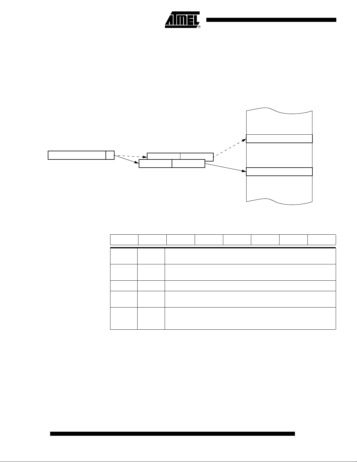
Dual-data Pointer
External Data Memory
AUXR1(A2H)
DPS
DPH(83H) DPL(82H)
07
DPTR0
DPTR1
Register (DPTR)
Figure 7. Use of Dual-data Pointer
The additional data pointer can be used to speed up code execution and reduce code
size in a number of ways.
The dual DPTR structure is a way by which the device will specify the address of an
external data memory location. There are two 16-bit DPTR registers that address the
external memory, and a single bit called DPS = AUXR1/bit0 (see Table 8) that allows
the program code to switch between them (Refer to Figure 7).
Table 8. AUXR1: Auxiliary Register 1
7 6 5 4 3 2 1 0
- - - - - 0 - DPS
Bit
Number
7-3 -
2 0 always stuck at 0
1 -
0 DPS
Bit
Mnemonic Description
Reserved
The value read from this bit is indeterminate. Do not set this bit.
Reserved
The value read from this bit is indeterminate. Do not set this bit.
Data Pointer Selection
Clear to select DPTR0.
Set to select DPTR1.
(1)
Reset Value = XXXX X0X0
Note: 1. User software should not write 1s to reserved bits. These bits may be used in future
8051 family products to invoke new features. In that case, the reset value of the new
bit will be 0, and its active value will be 1. The value read from a reserved bit is
indeterminate.
16
4134D–8051–02/08
Page 17

Application
Software can take advantage of the additional data pointers to both increase speed and
reduce code size, for example, block operations (copy, compare, search...) are well
served by using one data pointer as a ’source’ pointer and the other one as a "destination" pointer.
ASSEMBLY LANGUAGE
; Block move using dual data pointers
; Destroys DPTR0, DPTR1, A and PSW
; note: DPS exits opposite of entry state
; unless an extra INC AUXR1 is added
;
00A2 AUXR1 EQU 0A2H
;
0000 909000MOV DPTR,#SOURCE ; address of SOURCE
0003 05A2 INC AUXR1 ; switch data pointers
0005 90A000 MOV DPTR,#DEST ; address of DEST
0008 LOOP:
0008 05A2 INC AUXR1 ; switch data pointers
000A E0 MOVX A,@DPTR ; get a byte from SOURCE
000B A3 INC DPTR ; increment SOURCE address
000C 05A2 INC AUXR1 ; switch data pointers
000E F0 MOVX @DPTR,A ; write the byte to DEST
000F A3 INC DPTR ; increment DEST address
0010 70F6JNZ LOOP ; check for 0 terminator
0012 05A2 INC AUXR1 ; (optional) restore DPS
INC is a short (2 bytes) and fast (12 clocks) way to manipulate the DPS bit in the AUXR1
SFR. However, note that the INC instruction does not directly force the DPS bit to a particular state, but simply toggles it. In simple routines, such as the block move example,
only the fact that DPS is toggled in the proper sequence matters, not its actual value. In
other words, the block move routine works the same whether DPS is “0” or “1” on entry.
Observe that without the last instruction (INC AUXR1), the routine will exit with DPS in
the opposite state.
4134D–8051–02/08
17
Page 18
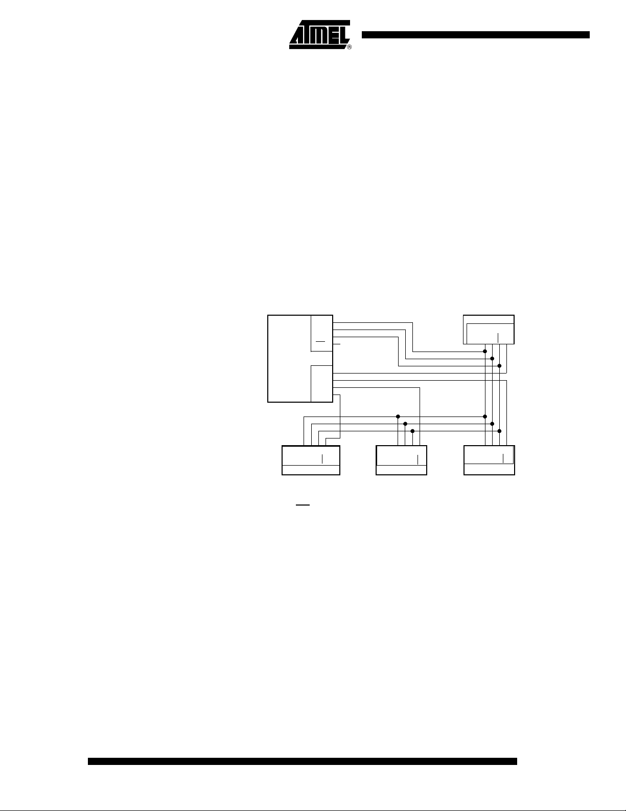
Serial Port Interface
Slave 1
MISO
MOSI
SCK
SS
MISO
MOSI
SCK
SS
PORT
0
1
2
3
Slave 3
MISO
MOSI
SCK
SS
Slave 4
MISO
MOSI
SCK
SS
Slave 2
MISO
MOSI
SCK
SS
V
DD
Master
(SPI)
The Serial Peripheral Interface module (SPI) which allows full-duplex, synchronous,
serial communication between the MCU and peripheral devices, including other MCUs.
Features
Signal Description
Features of the SPI module include the following:
• Full-duplex, three-wire synchronous transfers
• Master or Slave operation
• Eight programmable Master clock rates
• Serial clock with programmable polarity and phase
• Master Mode fault error flag with MCU interrupt capability
• Write collision flag protection
Figure 8 shows a typical SPI Bus configuration using one Master controller and many
Slave peripherals. The bus is made of three wires connecting all the devices.
Figure 8. Typical SPI Bus
The Master device selects the individual Slave devices by using four pins of a parallel
port to control the four SS pins of the Slave devices.
Master Output Slave Input (MOSI)
This 1-bit signal is directly connected between the Master device and a Slave device.
The MOSI line is used to transfer data in series from the Master to the Slave. Therefore,
it is an output signal from the Master, and an input signal to a Slave. A byte (8-bit word)
is transmitted most significant bit (MSB) first, least significant bit (LSB) last.
Master Input Slave Output (MISO)
This 1-bit signal is directly connected between the Slave device and a Master device.
The MISO line is used to transfer data in series from the Slave to the Master. Therefore,
it is an output signal from the Slave, and an input signal to the Master. A byte (8-bit
word) is transmitted most significant bit (MSB) first, least significant bit (LSB) last.
SPI Serial Clock (SCK) This signal is used to synchronize the data movement both in and out the devices
through their MOSI and MISO lines. It is driven by the Master for eight clock cycles
which allows to exchange one byte on the serial lines.
18
4134D–8051–02/08
Page 19
Slave Select (SS) Each Slave peripheral is selected by one Slave Select pin (SS). This signal must stay
low for any message for a Slave. It is obvious that only one Master (SS high level) can
drive the network. The Master may select each Slave device by software through port
pins (Figure 8). To prevent bus conflicts on the MISO line, only one slave should be
selected at a time by the Master for a transmission.
In a Master configuration, the SS line can be used in conjunction with the MODF flag in
the SPI Status register (SPSTA) to prevent multiple masters from driving MOSI and
SCK (See Error Conditions).
A high level on the SS pin puts the MISO line of a Slave SPI in a high-impedance state.
The SS pin could be used as a general purpose if the following conditions are met:
• The device is configured as a Master and the SSDIS control bit in SPCON is set.
This kind of configuration can be found when only one Master is driving the network
and there is no way that the SS pin will be pulled low. Therefore, the MODF flag in
the SPSTA will never be set
• The Device is configured as a Slave with CPHA and SSDIS control bits set
(1)
.
(2)
. This
kind of configuration can happen when the system comprises one Master and one
Slave only. Therefore, the device should always be selected and there is no reason
that the Master uses the SS pin to select the communicating Slave device.
Baud Rate In Master Mode, the baud rate can be selected from a baud rate generator which is con-
trolled by three bits in the SPCON register: SPR2, SPR1 and SPR0. The Master clock is
chosen from one of six clock rates resulting from the division of the internal clock by 4, 8,
16, 32, 64 or 128.
Table 9 gives the different clock rates selected by SPR2:SPR1:SPR0:
Table 9. SPI Master Baud Rate Selection
SPR2:SPR1:SPR0 Clock Rate Baud Rate Divisor (BD)
000 Don’t Use No BRG
001 F
010 F
011 F
100 F
101 F
110 F
111 Don’t Use No BRG
CLK_PERIPH
CLK_PERIPH
CLK_PERIPH
CLK_PERIPH
CLK_PERIPH
CLK_PERIPH
/4 4
/8 8
/16 16
/32 32
/64 64
/128 128
4134D–8051–02/08
1. Clearing SSDIS control bit does not clear MODF.
2. Special care should be taken not to set SSDIS control bit when CPHA = “0” because in
this mode, the SS is used to start the transmission.
19
Page 20

Functional Description
Shift Register
01
234567
Internal Bus
Pin
Control
Logic
MISO
MOSI
SCK
M
S
Clock
Logic
Clock
Divider
Clock
Select
/4
/64
/128
SPI Interrupt Request
8-bit bus
1-bit signal
SS
IntClk
/32
/8
/16
Receive Data Register
SPDAT
SPI
Control
SPSTA
CPHA
SPR0
SPR1
CPOLMSTRSSDISSPENSPR2
SPCON
WCOL MODFSPIF
-
- - - -
Figure 9 shows a detailed structure of the SPI module.
Figure 9. SPI Module Block Diagram
Operating Modes The Serial Peripheral Interface can be configured as one of the two modes: Master
Mode or Slave Mode. The configuration and initialization of the SPI module is made
through one register:
• The Serial Peripheral Control register (SPCON)
Once the SPI is configured, the data exchange is made using:
• SPCON
• The Serial Peripheral Status register (SPSTA)
• The Serial Peripheral Data register (SPDAT)
During an SPI transmission, data is simultaneously transmitted (shifted out serially) and
received (shifted in serially). A serial clock line (SCK) synchronizes shifting and sampling on the two serial data lines (MOSI and MISO). A Slave Select line (SS) allows
individual selection of a Slave SPI device; Slave devices that are not selected do not
interfere with SPI bus activities.
When the Master device transmits data to the Slave device via the MOSI line, the Slave
device responds by sending data to the Master device via the MISO line. This implies
full-duplex transmission with both data out and data in synchronized with the same clock
(Figure 10).
20
4134D–8051–02/08
Page 21

Figure 10. Full-Duplex Master-Slave Interconnection
8-bit Shift Register
SPI
Clock Generator
Master MCU
8-bit Shift Register
MISOMISO
MOSI
MOSI
SCK SCK
VSS
V
DD
SSSS
Slave MCU
Master Mode The SPI operates in Master Mode when the Master bit, MSTR
is set. Only one Master SPI device can initiate transmissions. Software begins the transmission from a Master SPI module by writing to the Serial Peripheral Data Register
(SPDAT). If the shift register is empty, the byte is immediately transferred to the shift
register. The byte begins shifting out on MOSI pin under the control of the serial clock,
SCK. Simultaneously, another byte shifts in from the Slave on the Master’s MISO pin.
The transmission ends when the Serial Peripheral transfer data flag, SPIF, in SPSTA
becomes set. At the same time that SPIF becomes set, the received byte from the Slave
is transferred to the receive data register in SPDAT. Software clears SPIF by reading
the Serial Peripheral Status register (SPSTA) with the SPIF bit set, and then reading the
SPDAT.
When the pin SS is pulled down during a transmission, the data is interrupted and when
the transmission is established again, the data present in the SPDAT is resent.
Slave Mode The SPI operates in Slave Mode when the Master bit, MSTR
(2)
cleared. Before a data transmission occurs, the Slave Select pin, SS, of the Slave
device must be set to “0”. SS must remain low until the transmission is complete.
In a Slave SPI module, data enters the shift register under the control of the SCK from
the Master SPI module. After a byte enters the shift register, it is immediately transferred
to the receive data register in SPDAT, and the SPIF bit is set. To prevent an overflow
condition, Slave software must then read the SPDAT before another byte enters the
shift register
(3)
. A Slave SPI must complete the write to the SPDAT (shift register) at
least one bus cycle before the Master SPI starts a transmission. If the write to the data
register is late, the SPI transmits the data already in the shift register from the previous
transmission.
(1)
, in the SPCON register
, in the SPCON register is
Transmission Formats Software can select any of four combinations of serial clock (SCK) phase and polarity
using two bits in the SPCON: the Clock POLarity (CPOL
(CPHA
(4)
). CPOL defines the default SCK line level in idle state. It has no significant
(4)
) and the Clock PHAse
effect on the transmission format. CPHA defines the edges on which the input data are
sampled and the edges on which the output data are shifted (Figure 11 and Figure 12).
The clock phase and polarity should be identical for the Master SPI device and the communicating Slave device.
1. The SPI module should be configured as a Master before it is enabled (SPEN set). Also
the Master SPI should be configured before the Slave SPI.
2. The SPI module should be configured as a Slave before it is enabled (SPEN set).
3. The maximum frequency of the SCK for an SPI configured as a Slave is the bus clock
speed.
4. Before writing to the CPOL and CPHA bits, the SPI should be disabled (SPEN = "0").
4134D–8051–02/08
21
Page 22

Figure 11. Data Transmission Format (CPHA = 0)
MSB bit6 bit5 bit4 bit3 bit2 bit1 LSB
bit6 bit5 bit4 bit3 bit2 bit1MSB LSB
1 32 4 5 6 7 8
Capture Point
SS (to Slave)
MISO (from Slave)
MOSI (from Master)
SCK (CPOL = 1)
SCK (CPOL = 0)
SPEN (Internal)
SCK Cycle Number
MSB bit6 bit5 bit4 bit3 bit2 bit1 LSB
bit6 bit5 bit4 bit3 bit2 bit1
MSB LSB
1 32 4 5 6 7 8
Capture Point
SS (to Slave)
MISO (from Slave)
MOSI (from Master)
SCK (CPOL = 1)
SCK (CPOL = 0)
SPEN (Internal)
SCK Cycle Number
Byte 1 Byte 2
Byte 3
MISO/MOSI
Master SS
Slave SS
(CPHA = 1)
Slave SS
(CPHA = 0)
Figure 12. Data Transmission Format (CPHA = 1)
22
As shown in Figure 11, the first SCK edge is the MSB capture strobe. Therefore, the
Slave must begin driving its data before the first SCK edge, and a falling edge on the SS
pin is used to start the transmission. The SS pin must be toggled high and then low
between each byte transmitted (Figure 13).
Figure 13. CPHA/SS Timing
Figure 12 shows an SPI transmission in which CPHA is “1”. In this case, the Master
begins driving its MOSI pin on the first SCK edge. Therefore the Slave uses the first
SCK edge as a start transmission signal. The SS pin can remain low between transmissions (Figure 13). This format may be preferable in systems having only one Master and
only one Slave driving the MISO data line.
4134D–8051–02/08
Page 23

Error Conditions The following flags in the SPSTA signal SPI error conditions.
Mode Fault (MODF) Mode Fault error in Master Mode SPI indicates that the level on the Slave Select (SS)
pin is inconsistent with the actual mode of the device. MODF is set to warn that there
may have a multi-master conflict for system control. In this case, the SPI system is
affected in the following ways:
• An SPI receiver/error CPU interrupt request is generated.
• The SPEN bit in SPCON is cleared. This disable the SPI.
• The MSTR bit in SPCON is cleared.
When SS DISable (SSDIS) bit in the SPCON register is cleared, the MODF flag is set
when the SS signal becomes “0”.
However, as stated before, for a system with one Master, if the SS pin of the Master
device is pulled low, there is no way that another Master is attempting to drive the network. In this case, to prevent the MODF flag from being set, software can set the SSDIS
bit in the SPCON register and therefore making the SS pin as a general-purpose I/O pin.
Clearing the MODF bit is accomplished by a read of SPSTA register with MODF bit set,
followed by a write to the SPCON register. SPEN Control bit may be restored to its original set state after the MODF bit has been cleared.
Write Collision (WCOL) A Write Collision (WCOL) flag in the SPSTA is set when a write to the SPDAT register is
done during a transmit sequence.
WCOL does not cause an interruption, and the transfer continues uninterrupted.
Clearing the WCOL bit is done through a software sequence of an access to SPSTA
and an access to SPDAT.
Overrun Condition An overrun condition occurs when the Master device tries to send several data bytes
and the Slave device has not cleared the SPIF bit issuing from the previous data byte
transmitted. In this case, the receiver buffer contains the byte sent after the SPIF bit was
last cleared. A read of the SPDAT returns this byte. All others bytes are lost.
This condition is not detected by the SPI peripheral.
SS Error Flag (SSERR) A Synchronous Serial Slave Error occurs when SS goes high before the end of a
received data in Slave Mode. SSERR does not cause in interruption, this bit is cleared
by writing 0 to SPEN bit (reset of the SPI state machine).
Interrupts Two SPI status flags can generate a CPU interrupt requests (See Table 10)
Table 10. SPI Interrupts
Flag Request
SPIF (SP data transfer) SPI Transmitter Interrupt request
MODF (Mode Fault) SPI Receiver/Error Interrupt Request (if SSDIS = "0")
Serial Peripheral data transfer flag, SPIF: This bit is set by hardware when a transfer
has been completed. SPIF bit generates transmitter CPU interrupt requests.
4134D–8051–02/08
Mode Fault flag, MODF: This bit becomes set to indicate that the level on the SS is
inconsistent with the mode of the SPI. MODF with SSDIS reset, generates receiver/error
CPU interrupt requests.
Figure 14 gives a logical view of the above statements.
23
Page 24

Figure 14. SPI Interrupt Requests Generation
SSDIS
MODF
CPU Interrupt Request
SPI Receiver/Error
CPU Interrupt Request
SPI Transmitter
SPI
CPU Interrupt Request
SPIF
Registers There are three registers in the module that provide control, status and data storage
functions. These registers are describes in the following paragraphs.
Serial Peripheral Control Register (SPCON)
The Serial Peripheral Control Register does the following:
• Selects one of the Master clock rates
• Configure the SPI module as Master or Slave
• Selects serial clock polarity and phase
• Enables the SPI module
• Frees the SS pin for a general purpose
Table 11 describes this register and explains the use of each bit.
Table 11. SPCON Register: Serial Peripheral Control Register - SPCON (S:C3h)
7 6 5 4 3 2 1 0
SPR2 SPEN SSDIS MSTR CPOL CPHA SPR1 SPR0
Bit
Number Bit Mnemonic R/W Mode Description
7 SPR2 R/W
6 SPEN R/W
5 SSDIS R/W
Serial Peripheral Rate 2
Bit with SPR1 and SPR0 define the clock rate
Serial Peripheral Enable
Clear to disable the SPI interface (internal reset of the SPI)
Set to enable the SPI interface
SS Disable
Clear to enable SS in both Master and Slave Modes
Set to disable SS in both Master and Slave Modes. In Slave Mode, this bit has no effect if CPHA = "0"
4 MSTR R/W
3 CPOL R/W
2 CPHA R/W
1 SPR1 R/W
24
Serial Peripheral Master
Clear to configure the SPI as a Slave
Set to configure the SPI as a Master
Clock Polarity
Clear to have the SCK set to ‘0’ in idle state
Set to have the SCK set to ’1’ in idle low
Clock Phase
Clear to have the data sampled when the SPSCK leaves the idle state (see CPOL)
Set to have the data sampled when the SPSCK returns to idle state (see CPOL)
Serial Peripheral Rate (SPR2:SPR1:SPR0)
000: N.A.
001: F
010: F
011: F
CLK PERIPH
CLK PERIPH
CLK PERIPH
/4
/8
/16
4134D–8051–02/08
Page 25

Bit
Number Bit Mnemonic R/W Mode Description
0 SPR0 R/W
100: F
CLK PERIPH
101: F
CLK PERIPH
110: F
CLK PERIPH
111: Don’t Use
/32
/64
/128
Reset Value = 00010100b
Serial Peripheral Status Register (SPSTA)
The Serial Peripheral Status Register contains flags to signal the following conditions:
• Data transfer complete
• Write collision
• Inconsistent logic level on SS pin (mode fault error)
Table 12 describes the SPSTA register and explains the use of every bit in the register.
Table 12. SPSTA: Serial Peripheral Status and Control Register - SPSTA (S:C4h)
7 6 5 4 3 2 1 0
SPIF WCOL SSERR MODF - - - -
Bit
Number Bit Mnemonic R/W Mode Description
Serial Peripheral Data Transfer Flag
7 SPIF R
6 WCOL R
Clear by hardware to indicate data transfer is in progress or has been approved by a clearing sequence.
Set by hardware to indicate that the data transfer has been completed.
Write Collision Flag
Cleared by hardware to indicate that no collision has occurred or has been approved by a clearing sequence.
Set by hardware to indicate that a collision has been detected.
5 SSERR R
4 MODF R
3 - R/W
2 - R/W
1 - R/W
0 - R/W
Reset Value = 00X0XXXXb
Synchronous Serial Slave Error Flag
Set by hardware when SS is deasserted before the end of a received data.
Cleared by disabling the SPI (clearing SPEN bit in SPCON).
Mode Fault
Cleared by hardware to indicate that the SS pin is at appropriate logic level, or has been approved by a
clearing sequence.
Set by hardware to indicate that the SS pin is at inappropriate logic level
Reserved
The value read from this bit is indeterminate. Do not set this bit.
Reserved
The value read from this bit is indeterminate. Do not set this bit.
Reserved
The value read from this bit is indeterminate. Do not set this bit.
Reserved
The value read from this bit is indeterminate. Do not set this bit.
4134D–8051–02/08
25
Page 26

Serial Peripheral Data Register (SPDAT)
The Serial Peripheral Data Register (Table 13) is a read/write buffer for the receive data
register. A write to SPDAT places data directly into the shift register. No transmit buffer
is available in this model.
A Read of the SPDAT returns the value located in the receive buffer and not the content
of the shift register.
Table 13. SPDAT (S:C5h): Serial Peripheral Data Register
7 6 5 4 3 2 1 0
R7 R6 R5 R4 R3 R2 R1 R0
Reset Value = XXXX XXXXb
R7:R0: Receive data bits
SPCON, SPSTA and SPDAT registers may be read and written at any time while there
is no on-going exchange. However, special care should be taken when writing to them
while a transmission is on-going:
• Do not change SPR2, SPR1 and SPR0
• Do not change CPHA and CPOL
• Do not change MSTR
• Clearing SPEN would immediately disable the peripheral
• Writing to the SPDAT will cause an overflow
26
4134D–8051–02/08
Page 27

Timers/Counters
The Errata Sheet implements two general-purpose, 16-bit Timers/Counters. They are
identified as Timer 0 and Timer 1, and can be independently configured to operate in a
variety of modes as a Timer or as an event Counter. When operating as a Timer, the
Timer/Counter runs for a programmed length of time, then issues an interrupt request.
When operating as a Counter, the Timer/Counter counts negative transitions on an
external pin. After a preset number of counts, the Counter issues an interrupt request.
The various operating modes of each Timer/Counter are described in the following
sections.
Timer/Counter Operations
For instance, a basic operation is Timer registers THx and TLx (x = 0, 1) connected in
cascade to form a 16-bit Timer. Setting the run control bit (TRx) in TCON register (see
Figure 14) turns the Timer on by allowing the selected input to increment TLx. When
TLx overflows it increments THx; when THx overflows it sets the Timer overflow flag
(TFx) in TCON register. Setting the TRx does not clear the THx and TLx Timer registers.
Timer registers can be accessed to obtain the current count or to enter preset values.
They can be read at any time but TRx bit must be cleared to preset their values,
other/wise the behavior of the Timer/Counter is unpredictable.
The C/Tx# control bit selects Timer operation or Counter operation by selecting the
divided-down peripheral clock or external pin Tx as the source for the counted signal.
TRx bit must be cleared when changing the mode of operation, other/wise the behavior
of the Timer/Counter is unpredictable.
For Timer operation (C/Tx# = 0), the Timer register counts the divided-down peripheral
clock. The Timer register is incremented once every peripheral cycle (6 peripheral clock
periods). The Timer clock rate is F
/6, i.e. F
PER
/12 in standard mode or F
OSC
OSC
/6 in X2
Mode.
For Counter operation (C/Tx# = 1), the Timer register counts the negative transitions on
the Tx external input pin. The external input is sampled every peripheral cycles. When
the sample is high in one cycle and low in the next one, the Counter is incremented.
Since it takes 2 cycles (12 peripheral clock periods) to recognize a negative transition,
the maximum count rate is F
/12, i.e. F
PER
/24 in standard mode or F
OSC
/12 in X2
OSC
Mode. There are no restrictions on the duty cycle of the external input signal, but to
ensure that a given level is sampled at least once before it changes, it should be held for
at least one full peripheral cycle.
Timer 0
4134D–8051–02/08
Timer 0 functions as either a Timer or event Counter in four modes of operation.
Figure 15 through Figure 18 show the logical configuration of each mode.
Timer 0 is controlled by the four lower bits of TMOD register (See Figure 15) and bits 0,
1, 4 and 5 of TCON register (see Figure 14). TMOD register selects the method of Timer
gating (GATE0), Timer or Counter operation (T/C0#) and mode of operation (M10 and
M00). TCON register provides Timer 0 control functions: overflow flag (TF0), run control
bit (TR0), interrupt flag (IE0) and interrupt type control bit (IT0).
For normal Timer operation (GATE0 = 0), setting TR0 allows TL0 to be incremented by
the selected input. Setting GATE0 and TR0 allows external pin INT0# to control Timer
operation.
Timer 0 overflow (count rolls over from all 1s to all 0s) sets TF0 flag generating an interrupt request.
It is important to stop Timer/Counter before changing mode.
27
Page 28

Mode 0 (13-bit Timer) Mode 0 configures Timer 0 as an 13-bit Timer which is set up as an 8-bit Timer (TH0
PERIPH
CLOCK
TRx
TCON Reg
TFx
TCON Reg
0
1
GATEx
TMOD Reg
÷
6
Overflow
Timer x
Interrupt
Request
C/Tx#
TMOD Reg
TLx
(5 Bits)
THx
(8 Bits)
INTx#
Tx
TRx
TCON Reg
TFx
TCON Reg
0
1
GATEx
TMOD Reg
Overflow
Timer x
Interrupt
Request
C/Tx#
TMOD Reg
TLx
(8 Bits)
THx
(8 Bits)
INTx#
Tx
PERIPH
CLOCK
÷
6
TRx
TCON Reg
TFx
TCON Reg
0
1
GATEx
TMOD Reg
Overflow
Timer x
Interrupt
Request
C/Tx#
TMOD Reg
TLx
(8 Bits)
THx
(8 Bits)
INTx#
Tx
PERIPH
CLOCK
÷
6
register) with a modulo 32 prescaler implemented with the lower five bits of TL0 register
(see Figure 15). The upper three bits of TL0 register are indeterminate and should be
ignored. Prescaler overflow increments TH0 register.
Figure 15. Timer/Counter x (x = 0 or 1) in Mode 0
Mode 1 (16-bit Timer) Mode 1 configures Timer 0 as a 16-bit Timer with TH0 and TL0 registers connected in
cascade (see Figure 16). The selected input increments TL0 register.
Figure 16. Timer/Counter x (x = 0 or 1) in Mode 1
Mode 2 (8-bit Timer with AutoReload)
Mode 2 configures Timer 0 as an 8-bit Timer (TL0 register) that automatically reloads
from TH0 register (see Figure 17). TL0 overflow sets TF0 flag in TCON register and
reloads TL0 with the contents of TH0, which is preset by software. When the interrupt
request is serviced, hardware clears TF0. The reload leaves TH0 unchanged. The next
reload value may be changed at any time by writing it to TH0 register.
Figure 17. Timer/Counter x (x = 0 or 1) in Mode 2
28
4134D–8051–02/08
Page 29

Mode 3 (Two 8-bit Timers) Mode 3 configures Timer 0 such that registers TL0 and TH0 operate as separate 8-bit
TR0
TCON.4
TF0
TCON.5
INT0
#
0
1
GATE0
TMOD.3
Overflow
Timer 0
Interrupt
Request
C/T0#
TMOD.2
TL0
(8 Bits)
TR1
TCON.6
TH0
(8 Bits)
TF1
TCON.7
Overflow
Timer 1
Interrupt
Request
T0
PERIPH
CLOCK
÷
6
PERIPH
CLOCK
÷
6
Timers (see Figure 18). This mode is provided for applications requiring an additional 8bit Timer or Counter. TL0 uses the Timer 0 control bits C/T0# and GATE0 in TMOD register, and TR0 and TF0 in TCON register in the normal manner. TH0 is locked into a
Timer function (counting F
/6) and takes over use of the Timer 1 interrupt (TF1) and
PER
run control (TR1) bits. Thus, operation of Timer 1 is restricted when Timer 0 is in Mode
3.
Figure 18. Timer/Counter 0 in Mode 3: Two 8-bit Counters
Timer 1
Timer 1 is identical to Timer 0 excepted for Mode 3 which is a hold-count mode. The following comments help to understand the differences:
• Timer 1 functions as either a Timer or event Counter in three modes of operation.
Figure 15 through Figure 17 show the logical configuration for modes 0, 1, and 2.
Timer 1’s Mode 3 is a hold-count mode.
• Timer 1 is controlled by the four high-order bits of TMOD register (see Figure 15)
and bits 2, 3, 6 and 7 of TCON register (see Figure 14). TMOD register selects the
method of Timer gating (GATE1), Timer or Counter operation (C/T1#) and mode of
operation (M11 and M01). TCON register provides Timer 1 control functions:
overflow flag (TF1), run control bit (TR1), interrupt flag (IE1) and interrupt type
control bit (IT1).
• Timer 1 can serve as the Baud Rate Generator for the Serial Port. Mode 2 is best
suited for this purpose.
• For normal Timer operation (GATE1 = 0), setting TR1 allows TL1 to be incremented
by the selected input. Setting GATE1 and TR1 allows external pin INT1# to control
Timer operation.
• Timer 1 overflow (count rolls over from all 1s to all 0s) sets the TF1 flag generating
an interrupt request.
• When Timer 0 is in Mode 3, it uses Timer 1’s overflow flag (TF1) and run control bit
(TR1). For this situation, use Timer 1 only for applications that do not require an
interrupt (such as a Baud Rate Generator for the Serial Port) and switch Timer 1 in
and out of Mode 3 to turn it off and on.
• It is important to stop Timer/Counter before changing mode.
4134D–8051–02/08
29
Page 30

Mode 0 (13-bit Timer) Mode 0 configures Timer 1 as a 13-bit Timer, which is set up as an 8-bit Timer (TH1 reg-
TF0
TCON.5
ET0
IE0.1
Timer 0
Interrupt Request
TF1
TCON.7
ET1
IE0.3
Timer 1
Interrupt Request
ister) with a modulo-32 prescaler implemented with the lower 5 bits of the TL1 register
(see Figure 15). The upper 3 bits of TL1 register are ignored. Prescaler overflow increments TH1 register.
Mode 1 (16-bit Timer) Mode 1 configures Timer 1 as a 16-bit Timer with TH1 and TL1 registers connected in
cascade (see Figure 16). The selected input increments TL1 register.
Mode 2 (8-bit Timer with AutoReload)
Mode 2 configures Timer 1 as an 8-bit Timer (TL1 register) with automatic reload from
TH1 register on overflow (see Figure 17). TL1 overflow sets TF1 flag in TCON register
and reloads TL1 with the contents of TH1, which is preset by software. The reload
leaves TH1 unchanged.
Mode 3 (Halt) Placing Timer 1 in Mode 3 causes it to halt and hold its count. This can be used to halt
Timer 1 when TR1 run control bit is not available i.e. when Timer 0 is in Mode 3.
Interrupt
Each Timer handles one interrupt source that is the timer overflow flag TF0 or TF1. This
flag is set every time an overflow occurs. Flags are cleared when vectoring to the Timer
interrupt routine. Interrupts are enabled by setting ETx bit in IE0 register. This assumes
interrupts are globally enabled by setting EA bit in IE0 register.
Figure 19. Timer Interrupt System
30
4134D–8051–02/08
Page 31

Registers
Table 14. TCON Register
TCON (S:88h)
Timer/Counter Control Register
7 6 5 4 3 2 1 0
TF1 TR1 TF0 TR0 IE1 IT1 IE0 IT0
Bit
Number
7 TF1
6 TR1
5 TF0
4 TR0
3 IE1
2 IT1
1 IE0
Bit
Mnemonic Description
Timer 1 Overflow Flag
Cleared by hardware when processor vectors to interrupt routine.
Set by hardware on Timer/Counter overflow, when Timer 1 register overflows.
Timer 1 Run Control Bit
Clear to turn off Timer/Counter 1.
Set to turn on Timer/Counter 1.
Timer 0 Overflow Flag
Cleared by hardware when processor vectors to interrupt routine.
Set by hardware on Timer/Counter overflow, when Timer 0 register overflows.
Timer 0 Run Control Bit
Clear to turn off Timer/Counter 0.
Set to turn on Timer/Counter 0.
Interrupt 1 Edge Flag
Cleared by hardware when interrupt is processed if edge-triggered (see IT1).
Set by hardware when external interrupt is detected on INT1# pin.
Interrupt 1 Type Control Bit
Clear to select low level active (level triggered) for external interrupt 1 (INT1#).
Set to select falling edge active (edge triggered) for external interrupt 1.
Interrupt 0 Edge Flag
Cleared by hardware when interrupt is processed if edge-triggered (see IT0).
Set by hardware when external interrupt is detected on INT0# pin.
4134D–8051–02/08
Interrupt 0 Type Control Bit
0 IT0
Clear to select low level active (level triggered) for external interrupt 0 (INT0#).
Set to select falling edge active (edge triggered) for external interrupt 0.
Reset Value = 0000 0000b
31
Page 32

Table 15. TMOD Register
TMOD (S:89h)
Timer/Counter Mode Control Register
7 6 5 4 3 2 1 0
GATE1 C/T1# M11 M01 GATE0 C/T0# M10 M00
Bit Number Bit Mnemonic Description
Timer 1 Gating Control Bit
7 GATE1
Clear to enable Timer 1 whenever TR1 bit is set.
Set to enable Timer 1 only while INT1# pin is high and TR1 bit is set.
6 C/T1#
5 M11
4 M01
3 GATE0
2 C/T0#
1 M10
0
M00
Reset Value = 0000 0000b
Timer 1 Counter/Timer Select Bit
Clear for Timer operation: Timer 1 counts the divided-down system clock.
Set for Counter operation: Timer 1 counts negative transitions on external pin T1.
Timer 1 Mode Select Bits
M11 M01 Operating Mode
0 0 Mode 0: 8-bit Timer/Counter (TH1) with 5-bit prescaler (TL1).
0 1 Mode 1: 16-bit Timer/Counter.
1 0 Mode 2: 8-bit auto-reload Timer/Counter (TL1). Reloaded from TH1 at overflow.
1 1 Mode 3: Timer 1 halted. Retains count.
Timer 0 Gating Control Bit
Clear to enable Timer 0 whenever TR0 bit is set.
Set to enable Timer/Counter 0 only while INT0# pin is high and TR0 bit is set.
Timer 0 Counter/Timer Select Bit
Clear for Timer operation: Timer 0 counts the divided-down system clock.
Set for Counter operation: Timer 0 counts negative transitions on external pin T0.
Timer 0 Mode Select Bit
M10 M00 Operating Mode
0 0 Mode 0: 8-bit Timer/Counter (TH0) with 5-bit prescaler (TL0).
0 1 Mode 1: 16-bit Timer/Counter.
1 0 Mode 2: 8-bit auto-reload Timer/Counter (TL0). Reloaded from TH0 at overflow.
1 1 Mode 3: TL0 is an 8-bit Timer/Counter.
TH0 is an 8-bit Timer using Timer 1’s TR0 and TF0 bits.
Table 16. TH0 Register
TH0 (S:8Ch)
32
Timer 0 High Byte Register
7 6 5 4 3 2 1 0
Bit
Number
7:0
Bit
Mnemonic Description
High Byte of Timer 0
Reset Value = 0000 0000b
4134D–8051–02/08
Page 33

Table 17. TL0 Register
TL0 (S:8Ah)
Timer 0 Low Byte Register
7 6 5 4 3 2 1 0
Bit
Number
7:0
Bit
Mnemonic Description
Low Byte of Timer 0
Reset Value = 0000 0000b
Table 18. TH1 Register
TH1 (S:8Dh)
Timer 1 High Byte Register
7 6 5 4 3 2 1 0
Bit Number Bit Mnemonic Description
7:0
High Byte of Timer 1
Reset Value = 0000 0000b
Table 19. TL1 Register
TL1 (S:8Bh)
Timer 1 Low Byte Register
7 6 5 4 3 2 1 0
4134D–8051–02/08
Bit Number
7:0
Bit
Mnemonic Description
Reset Value = 0000 0000b
Low Byte of Timer 1
33
Page 34

Power Management
Table 20. PCON Register
PCON - Power Control Register (87h)
7 6 5 4 3 2 1 0
- - - - GF1 GF0 PD IDL
Bit
Number
7 -
6 -
5 -
4 -
3 GF1
2 GF0
1 PD
0 IDL
Bit
Mnemonic Description
Reserved
The value read from this bit is indeterminate. Do not set this bit.
Reserved
The value read from this bit is indeterminate. Do not set this bit.
Reserved
The value read from this bit is indeterminate. Do not set this bit.
Reserved
The value read from this bit is indeterminate. Do not set this bit.
General-purpose Flag
Cleared by user for general purpose usage.
Set by user for general purpose usage.
General-purpose Flag
Cleared by user for general purpose usage.
Set by user for general purpose usage.
Power-Down Mode Bit
Cleared by hardware when reset occurs.
Set to enter Power-down Mode.
Idle Mode Bit
Cleared by hardware when interrupt or reset occurs.
Set to enter Idle Mode.
Idle Mode
Reset Value = XXX1 0000b
Not bit addressable
An instruction that sets PCON.0 indicates that it is the last instruction to be executed
before going into the Idle Mode. In the Idle Mode, the internal clock signal is gated off to
the CPU, but not to the interrupt, Timer, and Serial Port functions. The CPU status is
preserved in its entirety: the Stack Pointer, Program Counter, Program Status Word,
Accumulator and all other registers maintain their data during Idle. The port pins hold
the logical states they had at the time Idle was activated.
There are two ways to terminate the Idle Mode. Activation of any enabled interrupt will
cause PCON.0 to be cleared by hardware, terminating the Idle Mode. The interrupt will
be serviced, and following RETI the next instruction to be executed will be the one following the instruction that put the device into idle.
The flag bits GF0 and GF1 can be used to give an indication if an interrupt occurred during normal operation or during an Idle. For example, an instruction that activates Idle
can also set one or both flag bits. When Idle is terminated by an interrupt, the interrupt
service routine can examine the flag bits.
The other way of terminating the Idle Mode is with a hardware reset. Since the clock
oscillator is still running, the hardware reset needs to be held active for only two
machine cycles (24 oscillator periods) to complete the reset.
34
4134D–8051–02/08
Page 35

Power-down Mode
INT1
INT0
XTALA
Power-down Phase Oscillator Restart Phase
Active PhaseActive Phase
or
XTALB
To save maximum power, a power-down mode can be invoked by software (refer to
Table 20, PCON register).
In power-down mode, the oscillator is stopped and the instruction that invoked powerdown mode is the last instruction executed. The internal RAM and SFRs retain their
value until the power-down mode is terminated. VCC can be lowered to save further
power. Either a hardware reset or an external interrupt can cause an exit from powerdown. To properly terminate power-down mode, the reset or external interrupt should
not be executed before VCC is restored to its normal operating level and must be held
active long enough for the oscillator to restart and stabilize.
Only external interrupts INT0, INT1 are useful for exiting from power-down. For that,
interrupt must be enabled and configured as level or edge sensitive interrupt input.
Holding the pin low restarts the oscillator but bringing the pin high completes the exit as
detailed in Figure 20. When both interrupts are enabled, the oscillator restarts as soon
as one of the two inputs is held low and power-down exit will be completed when the first
input is released. In this case the higher priority interrupt service routine is executed.
Once the interrupt is serviced, the next instruction to be executed after RETI will be the
one following the instruction that put AT8xC5103 into power-down mode.
Figure 20. Power-Down Exit Waveform
4134D–8051–02/08
Exiting from power-down by reset redefines all the SFRs, exiting from power-down by
external interrupt does no affect the SFRs.
Exiting from power-down by either reset or external interrupt does not affect the internal
RAM content.
Note: If idle mode is activated with power-down mode (IDL and PD bits set), the exit sequence
is unchanged, when execution is vectored to interrupt, PD and IDL bits are cleared and
idle mode is not entered.
Table 21 shows the state of ports during idle and power-down modes.
Table 21. State of Ports
Mode Program Memory PORT1 PORT3
Idle Internal Port Data Port Data
Power-down Internal Port Data Port Data
Note: 1. Port 0 can force a 0 level. A ‘one’ will leave port floating.
(1)
35
Page 36

Programmable Counter Array (PCA)
The PCA provides more timing capabilities with less CPU intervention than the standard
timer/counters. Its advantages include reduced software overhead and improved accuracy. The PCA consists of a dedicated timer/counter which serves as the time base for
an array of five compare/capture modules. Its clock input can be programmed to count
any one of the following signals:
• Oscillator frequency ÷ 12 (÷ 6 in X2 Mode)
• Oscillator frequency ÷ 4 (÷ 2 in X2 Mode)
• Timer 0 overflow
• External input on ECI (P1.2)
Each compare/capture modules can be programmed in any one of the following modes:
• Rising and/or falling edge capture,
• Software timer
• High-speed output
• Pulse width modulator
Module 4 can also be programmed as a watchdog timer.
When the compare/capture modules are programmed in the capture mode, software
timer, or high speed output mode, an interrupt can be generated when the module executes its function. All five modules and the PCA timer overflow share one interrupt
vector.
The PCA timer/counter and compare/capture modules share Port 1 for external I/O.
These pins are listed below. If the port is not used for the PCA, it can still be used for
standard I/O.
PCA Component External I/O Pin
16-bit Counter P1.2/ECI
16-bit Module 0 P1.3/CEX0
16-bit Module 1 P1.4/CEX1
16-bit Module 2 P1.5/CEX2
16-bit Module 3 P1.6/CEX3
16-bit Module 4 P1.7/CEX4
The PCA timer is a common time base for all five modules (See Figure 21). The timer
count source is determined from the CPS1 and CPS0 bits in the CMOD SFR (see
Table 21) and can be programmed to run at:
• 1/12 the oscillator frequency (or 1/6 in X2 Mode)
• 1/4 the oscillator frequency (or 1/2 in X2 Mode)
• The Timer 0 overflow
• The input on the ECI pin (P1.2)
36
4134D–8051–02/08
Page 37

PCA Timer
CIDL CPS1 CPS0 ECF
It
CH CL
16-bit Up/Down Counter
To PCA
Modules
Fosc/12
Fosc/4
T0 OVF
P1.2
Idle
CMOD
0xD9
WDTE
CF CR
CCON
0xD8
CCF4 CCF3 CCF2 CCF1 CCF0
Overflow
Figure 21. PCA Timer/Counter
Table 22. CMOD: PCA Counter Mode Register
CMOD
Address 0D9H CIDL WDTE - - - CPS1 CPS0 ECF
Reset value 0 0 X X X 0 0 0
Symbol Function
CIDL
WDTE Watchdog Timer Enable: WDTE = 0 disables Watchdog Timer function on PCA Module 4. WDTE = 1 enables it.
- Not implemented, reserved for future use.
CPS1 PCA Count Pulse Select bit 1.
CPS0 PCA Count Pulse Select bit 0.
ECF
Counter Idle control: CIDL = 0 programs the PCA Counter to continue functioning during idle Mode. CIDL = 1 programs it to be
gated off during idle.
CPS1 CPS0 Selected PCA input.
0 0 Internal clock f
0 1 Internal clock f
1 0 Timer 0 Overflow
1 1 External clock at ECI/P1.2 pin (max rate = f
PCA Enable Counter Overflow interrupt: ECF = 1 enables CF bit in CCON to generate an interrupt. ECF = 0 disables that
function of CF.
(1)
(2)
/12 (Or f
osc
/4 (Or f
osc
/6 in X2 Mode).
osc
/2 in X2 Mode).
osc
/ 8)
osc
1. User software should not write 1s to reserved bits. These bits may be used in future 8051 family products to invoke new features. In that case, the reset or inactive value of the new bit will be 0, and its active value will be 1. The value read from a
reserved bit is indeterminate.
2. f
4134D–8051–02/08
= oscillator frequency
osc
37
Page 38

The CMOD SFR includes three additional bits associated with the PCA (See Figure 21
and Table 21).
• The CIDL bit which allows the PCA to stop during idle mode.
• The WDTE bit which enables or disables the watchdog function on module 4.
• The ECF bit which when set causes an interrupt and the PCA overflow flag CF (in
the CCON SFR) to be set when the PCA timer overflows.
The CCON SFR contains the run control bit for the PCA and the flags for the PCA timer
(CF) and each module (Refer to Table 23).
• Bit CR (CCON.6) must be set by software to run the PCA. The PCA is shut off by
clearing this bit.
• Bit CF: The CF bit (CCON.7) is set when the PCA counter overflows and an
interrupt will be generated if the ECF bit in the CMOD register is set. The CF bit can
only be cleared by software.
• Bits 0 through 4 are the flags for the modules (bit 0 for module 0, bit 1 for module 1,
etc.) and are set by hardware when either a match or a capture occurs. These flags
also can only be cleared by software.
•
Table 23. CCON: PCA Counter Control Register
CCON
Address 0D8H
Reset Value 0 0 X 0 0 0 0 0
Symbol Function
PCA Counter Overflow flag. Set by hardware when the counter rolls over. CF flags
CF
CR
- Not implemented, reserved for future use.
CCF4
CCF3
CCF2
CCF1
CCF0
an interrupt if bit ECF in CMOD is set. CF may be set by either hardware or software but
can only be cleared by software.
PCA Counter Run control bit. Set by software to turn the PCA counter on. Must be cleared
by software to turn the PCA counter off.
PCA Module 4 interrupt flag. Set by hardware when a match or capture occurs. Must be
cleared by software.
PCA Module 3 interrupt flag. Set by hardware when a match or capture occurs. Must be
cleared by software.
PCA Module 2 interrupt flag. Set by hardware when a match or capture occurs. Must be
cleared by software.
PCA Module 1 interrupt flag. Set by hardware when a match or capture occurs. Must be
cleared by software.
PCA Module 0 interrupt flag. Set by hardware when a match or capture occurs. Must be
cleared by software.
CF CR - CCF4 CCF3 CCF2 CCF1 CCF0
(1)
38
1. User software should not write 1s to reserved bits. These bits may be used in future 8051
family products to invoke new features. In that case, the reset or inactive value of the
new bit will be 0, and its active value will be 1. The value read from a reserved bit is
indeterminate.
The watchdog timer function is implemented in module 4 (See Figure 24).
The PCA interrupt system is shown in Figure 22.
4134D–8051–02/08
Page 39

Figure 22. PCA Interrupt System
CF CR
CCON
0xD8
CCF4 CCF3 CCF2 CCF1 CCF0
Module 4
Module 3
Module 2
Module 1
Module 0
ECF
PCA Timer/Counter
ECCFn
CCAPMn.0CMOD.0
IE.6 IE.7
To Interrupt
Priority Decoder
EC EA
PCA Modules: each one of the five compare/capture modules has six possible functions. It can perform:
• 16-bit Capture, positive-edge triggered
• 16-bit Capture, negative-edge triggered
• 16-bit Capture, both positive and negative-edge triggered
• 16-bit Software Timer
• 16-bit High Speed Output
• 8-bit Pulse Width Modulator
4134D–8051–02/08
In addition, module 4 can be used as a Watchdog Timer.
Each module in the PCA has a special function register associated with it. These registers are: CCAPM0 for module 0, CCAPM1 for module 1, etc. (See Table 24). The
registers contain the bits that control the mode that each module will operate in.
• The ECCF bit (CCAPMn.0 where n = 0, 1, 2, 3, or 4 depending on the module)
enables the CCF flag in the CCON SFR to generate an interrupt when a match or
compare occurs in the associated module.
• PWM (CCAPMn.1) enables the pulse width modulation mode.
• The TOG bit (CCAPMn.2) when set causes the CEX output associated with the
module to toggle when there is a match between the PCA counter and the module's
capture/compare register.
• The match bit MAT (CCAPMn.3) when set will cause the CCFn bit in the CCON
register to be set when there is a match between the PCA counter and the module's
capture/compare register.
• The next two bits CAPN (CCAPMn.4) and CAPP (CCAPMn.5) determine the edge
that a capture input will be active on. The CAPN bit enables the negative edge, and
the CAPP bit enables the positive edge. If both bits are set both edges will be
enabled and a capture will occur for either transition.
• The last bit in the register ECOM (CCAPMn.6) when set enables the comparator
function.
39
Page 40

Table 24 shows the CCAPMn settings for the various PCA functions.
Table 24. CCAPMn: PCA Modules Compare/Capture Control Registers
CCAPM0 (0DAH)
CCAPMn
Address
n = 0 - 4
Symbol Function
ECOMn Enable Comparator. ECOMn = 1 enables the comparator function.
CAPPn Capture Positive, CAPPn = 1 enables positive edge capture.
CAPNn Capture Negative, CAPNn = 1 enables negative edge capture.
CCAPM1 (0DBH)
CCAPM2 (0DCH)
CCAPM3 (0DDH)
CCAPM4 (0DEH)
- ECOMn CAPPn CAPNn MATn TOGn PWMm ECCFn
Reset value X 0 0 0 0 0 0 0
- Not implemented, reserved for future use.
(1)
MATn
TOGn
PWMn
ECCFn
Match. When MATn = 1, a match of the PCA counter with this module's compare/capture
register causes the CCFn bit in CCON to be set, flagging an interrupt.
Toggle. When TOGn = 1, a match of the PCA counter with this module's compare/capture
register causes the CEXn pin to toggle.
Pulse Width Modulation Mode. PWMn = 1 enables the CEXn pin to be used as a pulse
width modulated output.
Enable CCF interrupt. Enables compare/capture flag CCFn in the CCON register to
generate an interrupt.
1. User software should not write 1s to reserved bits. These bits may be used in future 8051
family products to invoke new features. In that case, the reset or inactive value of the
new bit will be 0, and its active value will be 1. The value read from a reserved bit is
indeterminate.
Table 25. PCA Module Modes (CCAPMn Registers)
ECOMn CAPPn CAPNn MATn TOGn PWMm ECCFn Module Function
0 0 0 0 0 0 0 No Operation
X 1 0 0 0 0 X
X 0 1 0 0 0 X
X 1 1 0 0 0 X
16-bit capture by a positive-edge
trigger on CEXn
16-bit capture by a negative trigger
on CEXn
16-bit capture by a transition on
CEXn
40
1 0 0 1 0 0 X
1 0 0 1 1 0 X 16-bit High Speed Output
1 0 0 0 0 1 0 8-bit PWM
1 0 0 1 X 0 X Watchdog Timer (module 4 only)
16-bit Software Timer/Compare
mode.
4134D–8051–02/08
Page 41

There are two additional registers associated with each of the PCA modules. They are
CCAPnH and CCAPnL and these are the registers that store the 16-bit count when a
capture occurs or a compare should occur. When a module is used in the PWM mode
these registers are used to control the duty cycle of the output (See Table 26 &
Table 27)
Table 26. CCAPnH: PCA Modules Capture/Compare Registers High
CCAP0H (0FAH)
CCAPnH
Address
n = 0 - 4
CCAP1H (0FBH)
CCAP2H (0FCH)
CCAP3H (0FDH)
CCAP4H (0FEH)
7 6 5 4 3 2 1 0
Reset value 0 0 0 0 0 0 0 0
Table 27. CCAPnL: PCA Modules Capture/Compare Registers Low
CCAP0L (0EAH)
CCAPnL
Address
n = 0 - 4
CCAP1L (0EBH)
CCAP2L (0ECH)
CCAP3L (0EDH)
CCAP4L (0EEH)
7 6 5 4 3 2 1 0
Reset value 0 0 0 0 0 0 0 0
Table 28. CH: PCA Counter High
CH
Address
0F9H
7 6 5 4 3 2 1 0
Reset value 0 0 0 0 0 0 0 0
Table 29. CL: PCA Counter Low
CL
Address
0E9H
7 6 5 4 3 2 1 0
Reset value 0 0 0 0 0 0 0 0
4134D–8051–02/08
41
Page 42

PCA Capture Mode
CF CR
CCON
0xD8
CH CL
CCAPnH CCAPnL
CCF4 CCF3 CCF2 CCF1 CCF0
PCA IT
PCA Counter/Timer
ECOMn
CCAPMn, n = 0 to 4
0xDA to 0xDE
CAPNn MATn TOGn PWMn ECCFnCAPPn
Cex.n
Capture
Figure 23. PCA Capture Mode
To use one of the PCA modules in the capture mode either one or both of the CCAPM
bits CAPN and CAPP for that module must be set. The external CEX input for the module (on port 1) is sampled for a transition. When a valid transition occurs the PCA
hardware loads the value of the PCA counter registers (CH and CL) into the module's
capture registers (CCAPnL and CCAPnH). If the CCFn bit for the module in the CCON
SFR and the ECCFn bit in the CCAPMn SFR are set then an interrupt will be generated
(see Figure 23).
42
4134D–8051–02/08
Page 43

16-bit Software Timer/
CH CL
CCAPnH CCAPnL
ECOMn
CCAPMn, n = 0 to 4
0xDA to 0xDE
CAPNn MATn TOGn PWMn ECCFnCAPPn
16 bit comparator
Match
CCON
0xD8
PCA IT
Enable
PCA counter/timer
RESET
(1)
CIDL CPS1 CPS0 ECF
CMOD
0xD9
WDTE
Reset
Write to
CCAPnL
Write to
CCAPnH
CF CCF2 CCF1 CCF0
CR
CCF3
CCF4
1 0
Compare Mode
The PCA modules can be used as software timers by setting both the ECOM and MAT
bits in the modules CCAPMn register. The PCA timer will be compared to the module's
capture registers and when a match occurs an interrupt will occur if the CCFn (CCON
SFR) and the ECCFn (CCAPMn SFR) bits for the module are both set (see Figure 24).
Figure 24. PCA Compare Mode and PCA Watchdog Timer
Note: 1. Only for Module 4
Before enabling ECOM bit, CCAPnL and CCAPnH should be set with a non zero value,
other/wise an unwanted match could happen. Writing to CCAPnH will set the ECOM bit.
Once ECOM set, writing CCAPnL will clear ECOM so that an unwanted match doesn’t
occur while modifying the compare value. Writing to CCAPnH will set ECOM. For this
reason, user software should write CCAPnL first, and then CCAPnH. Of course, the
ECOM bit can still be controlled by accessing to CCAPMn register.
4134D–8051–02/08
43
Page 44

High Speed Output Mode
CH CL
CCAPnH CCAPnL
ECOMn
CCAPMn, n = 0 to 4
0xDA to 0xDE
CAPNn MATn TOGn PWMn ECCFnCAPPn
16-bit Comparator
Match
CF CR
CCON
0xD8
CCF4 CCF3 CCF2 CCF1 CCF0
PCA IT
Enable
CEXn
PCA Counter/Timer
Write to
CCAPnH
Reset
Write to
CCAPnL
1
0
In this mode the CEX output (on port 1) associated with the PCA module will toggle
each time a match occurs between the PCA counter and the module's capture registers.
To activate this mode the TOG, MAT, and ECOM bits in the module's CCAPMn SFR
must be set (see Figure 25).
A prior write must be done to CCAPnL and CCAPnH before writing the ECOMn bit.
Figure 25. PCA High Speed Output Mode
Pulse Width Modulator Mode
Before enabling ECOM bit, CCAPnL and CCAPnH should be set with a non zero value,
other/wise an unwanted match could happen.
Once ECOM set, writing CCAPnL will clear ECOM so that an unwanted match doesn’t
occur while modifying the compare value. Writing to CCAPnH will set ECOM. For this
reason, user software should write CCAPnL first, and then CCAPnH. Of course, the
ECOM bit can still be controlled by accessing to CCAPMn register.
All of the PCA modules can be used as PWM outputs. Figure 26 shows the PWM function. The frequency of the output depends on the source for the PCA timer. All of the
modules will have the same frequency of output because they all share the PCA timer.
The duty cycle of each module is independently variable using the module's capture
register CCAPLn. When the value of the PCA CL SFR is less than the value in the module's CCAPLn SFR the output will be low, when it is equal to or greater than the output
will be high. When CL overflows from FF to 00, CCAPLn is reloaded with the value in
CCAPHn. This allows updating the PWM without glitches. The PWM and ECOM bits in
the module's CCAPMn register must be set to enable the PWM mode.
44
4134D–8051–02/08
Page 45

Figure 26. PCA PWM Mode
CL
CCAPnH
CCAPnL
ECOMn
CCAPMn, n = 0 to 4
0xDA to 0xDE
CAPNn MATn TOGn PWMn ECCFnCAPPn
8-bit Comparator
CEXn
“0”
“1”
≥
<
Enable
PCA Counter/Timer
Overflow
PCA Watchdog Timer
An on-board watchdog timer is available with the PCA to improve the reliability of the
system without increasing chip count. Watchdog timers are useful for systems that are
susceptible to noise, power glitches, or electrostatic discharge. Module 4 is the only
PCA module that can be programmed as a watchdog. However, this module can still be
used for other modes if the watchdog is not needed. Figure 24 shows a diagram of how
the watchdog works. The user pre-loads a 16-bit value in the compare registers. Just
like the other compare modes, this 16-bit value is compared to the PCA timer value. If a
match is allowed to occur, an internal reset will be generated. This will not cause the
RST pin to be driven high.
In order to hold off the reset, the user has three options:
1. Periodically change the compare value so it will never match the PCA timer.
2. Periodically change the PCA timer value so it will never match the compare
values.
3. Disable the watchdog by clearing the WDTE bit before a match occurs and then
re-enable it.
The first two options are more reliable because the watchdog timer is never disabled as
in option #3. If the program counter ever goes astray, a match will eventually occur and
cause an internal reset. The second option is also not recommended if other PCA modules are being used. Remember, the PCA timer is the time base for all modules;
changing the time base for other modules would not be a good idea. Thus, in most applications the first solution is the best option.
This watchdog timer won’t generate a reset out on the reset pin.
4134D–8051–02/08
45
Page 46

Interrupt System
IE1
0
3
High Priority
Interrupt
Interrupt
Polling
Sequence
Low Priority
Interrupt
Global
Disable
Individual
Enable
NC
NC
TF0
INT0
INT1
TF1
IPH, IP
IE0
0
3
0
3
0
3
0
3
0
3
NC
SPI
0
3
NC
0
3
0
3
CF
CCFx
PCA
NC
The AT8xC5103 has a total of 5 interrupt vectors: one external interrupt INT0, two timer
interrupts (timers 0, 1), PCA and SPI. These interrupts are shown in Figure 27..
Figure 27. Interrupt Control System
Each of the interrupt sources can be individually enabled or disabled by setting or clearing a bit in the Interrupt Enable register (see Table 31). This register also contains a
global disable bit, which must be cleared to disable all interrupts at once.
Each interrupt source can also be individually programmed to one of four priority levels
by setting or clearing a bit in the Interrupt Priority register (see Table 33) and in the Interrupt Priority High register (see Table 35). Table 30 shows the bit values and priority
levels associated with each combination.
46
4134D–8051–02/08
Page 47

Table 30. Priority Level Bit Values
IPH.x IPL.x Interrupt Level Priority
0 0 0 (Lowest)
0 1 1
1 0 2
1 1 3 (Highest)
A low-priority interrupt can be interrupted by a high priority interrupt, but not by another
low-priority interrupt. A high-priority interrupt can’t be interrupted by any other interrupt
source.
If two interrupt requests of different priority levels are received simultaneously, the
request of higher priority level is serviced. If interrupt requests of the same priority level
are received simultaneously, an internal polling sequence determines which request is
serviced. Thus within each priority level there is a second priority structure determined
by the polling sequence.
Interrupt Name Interrupt Address Vector Priority Number
External Interrupt (INT0) 0003h 1
Timer0 (TF0) 000Bh 2
External Interrupt (INT1) 0013h 3
Timer1 (TF1) 001Bh 4
PCA (CF or CCFn) 0033h 5
SPI 004Bh 6
.
4134D–8051–02/08
47
Page 48

Table 31. IE0 Register
IE0 (S:A8h)
Interrupt Enable Register
7 6 5 4 3 2 1 0
EA EC - - ET1 EX1 ET0 EX0
Bit
Number
7 EA
6 EC
5 -
4 -
3 ET1
2 EX1
1 ET0
Bit
Mnemonic Description
Enable All Interrupt Bit
Clear to disable all interrupts.
Set to enable all interrupts.
If EA=1, each interrupt source is individually enabled or disabled by setting or
clearing its interrupt enable bit.
PCA Interrupt Enable
Clear to disable the PCA interrupt.
Set to enable the PCA interrupt.
Reserved
The value read from this bit is indeterminate. Do not set this bit.
Reserved
The value read from this bit is indeterminate. Do not set this bit.
Timer 1 overflow interrupt Enable bit
Clear to disable timer 1 overflow interrupt.
Set to enable timer 1 overflow interrupt.
External Interrupt 1 Enable bit
Clear to disable external interrupt 0.
Set to enable external interrupt 0.
Timer 0 Overflow Interrupt Enable bit
Clear to disable timer 0 overflow interrupt.
Set to enable timer 0 overflow interrupt.
48
0 EX0
External Interrupt 0 Enable bit
Clear to disable external interrupt 0.
Set to enable external interrupt 0.
Reset Value = 00XX 0000b
Bit addressable
4134D–8051–02/08
Page 49

Table 32. IE1 Register
IE1 (S:B1h)
Interrupt Enable Register
7 6 5 4 3 2 1 0
- - - - - ESPI - -
Bit
Number
7 -
6 -
5 -
4 -
3 -
2 ESPI
1 -
0 -
Bit
Mnemonic Description
Reserved
The value read from this bit is indeterminate. Do not set this bit.
Reserved
The value read from this bit is indeterminate. Do not set this bit.
Reserved
The value read from this bit is indeterminate. Do not set this bit.
Reserved
The value read from this bit is indeterminate. Do not set this bit.
Reserved
The value read from this bit is indeterminate. Do not set this bit.
SPI Interrupt Enable bit
Clear to disable the SPI interrupt.
Set to enable the SPI interrupt.
Reserved
The value read from this bit is indeterminate. Do not set this bit.
Reserved
The value read from this bit is indeterminate. Do not set this bit.
Reset Value = XXXX X0XXb
No Bit addressable
4134D–8051–02/08
49
Page 50

Table 33. IPL0 Register
IPH0 - Interrupt Priority Low Register 0
7 6 5 4 3 2 1 0
- PPCL - - PT1L PX1L PT0L PX0L
Bit
Number
7 -
6 PPCL
5 -
4 -
3 PT1L
2 PX1L
1 PT0L
0 PX0L
Bit
Mnemonic Description
Reset Value = X0XX 0000b
Bit addressable.
Reserved
The value read from this bit is indeterminate. Do not set this bit.
PCA Counter Interrupt Priority bit
Refer to PPCH for priority level
Reserved
The value read from this bit is indeterminate. Do not set this bit.
Reserved
The value read from this bit is indeterminate. Do not set this bit.
Timer 1 Overflow Interrupt Priority bit
Refer to PT1H for priority level.
External Interrupt 1Priority bit
Refer to PX1H for priority level.
Timer 0 Overflow Interrupt Priority bit
Refer to PT0H for priority level.
External Interrupt 0 Priority bit
Refer to PX0H for priority level.
50
4134D–8051–02/08
Page 51

Table 34. IPL1 Register
IPL1 (S:B2h)
IPL1 - Interrupt Priority Low Register 1
7 6 5 4 3 2 1 0
- - - - - PSPIL - -
Bit Number
7
6 -
5 -
4 -
3 -
2 PSPIL
1 -
0 -
Bit
Mnemonic Description
Reserved
The value read from this bit is indeterminate. Do not set this bit.
Reserved
The value read from this bit is indeterminate. Do not set this bit.
Reserved
The value read from this bit is indeterminate. Do not set this bit.
Reserved
The value read from this bit is indeterminate. Do not set this bit.
SPI Interrupt Priority Level Less Significant bit.
Refer to PSPIH for priority level.
Reserved
The value read from this bit is indeterminate. Do not set this bit.
Reserved
The value read from this bit is indeterminate. Do not set this bit.
Reset Value = XXXX X0XXb
Not Bit addressable.
4134D–8051–02/08
51
Page 52

Table 35. IPH0 Register
IPH0 (S:B7h)
IPH0 - Interrupt Priority High Register 0
7 6 5 4 3 2 1 0
- PPCH - - PT1H PX1H PT0H PX0H
Bit
Number
7 -
6 PPCH
5 -
4 -
3 PT1H
2 PX1H
Bit
Mnemonic Description
Reserved
The value read from this bit is indeterminate. Do not set this bit.
PCA Counter Interrupt Priority Level Most Significant bit
PPCH PPCL Priority level
0 0 Lowest
0 1
1 0
1 1 Highest priority
Reserved
The value read from this bit is indeterminate. Do not set this bit.
Reserved
The value read from this bit is indeterminate. Do not set this bit.
Timer 1 overflow interrupt Priority High bit
PT1H PT1L Priority Level
0 0 Lowest
0 1
1 0
1 1 Highest
External interrupt 1Priority High bit
PX1H PX1L Priority Level
0 0 Lowest
0 1
1 0
1 1 Highest
52
1 PT0H
0 PX0H
Reset Value = X0XX 0000b
Not bit addressable
Timer 0 overflow interrupt Priority High bit
PT0H PT0L Priority Level
0 0 Lowest
0 1
1 0
1 1 Highest
External interrupt 0 Priority High bit
PX0H PX0L Priority Level
0 0 Lowest
0 1
1 0
1 1 Highest
4134D–8051–02/08
Page 53

Table 36. IPH1 Register
IPH1 - Interrupt Priority High Register 1 (B3h)
7 6 5 4 3 2 1 0
- - - - - PSPIH - -
Bit Number
7
6 -
5 -
4 -
3 -
2 PSPIH
1 -
0 -
Bit
Mnemonic Description
Reserved
The value read from this bit is indeterminate. Do not set this bit.
Reserved
The value read from this bit is indeterminate. Do not set this bit.
Reserved
The value read from this bit is indeterminate. Do not set this bit.
Reserved
The value read from this bit is indeterminate. Do not set this bit.
SPI Interrupt Priority Level Most Significant bit
PSPIH PSPIL Priority level
0 0 Lowest
0 1
1 0
1 1 Highest
Reserved
The value read from this bit is indeterminate. Do not set this bit.
Reserved
The value read from this bit is indeterminate. Do not set this bit.
Reset Value = XXXX X0XXb
Not bit addressable
4134D–8051–02/08
53
Page 54

Hardware Byte: Lock bit
Table 37. Hardware Byte (HSB)
7 6 5 4 3 2 1 0
- LB - - - - - -
Bit Number Bit Mnemonic Description
7 -
6 LB
5:0 -
Reserved
Do not write this bi
User Program EPROM Lock Bit
Programmed (0) to protect memory from external read
Unprogrammed (1), read or write is allowed
Reserved
Do not write these bits
t
The Lock system, when programmed, protects the on-chip program against software
piracy. Only one level of protection for the on-chip code which when programmed are
provided. If lock bit program, no read operation can be done, only CRC check.
This security bit is accessible only with hardware programmer.
54
4134D–8051–02/08
Page 55

Electrical Characteristics
Absolute Maximum Ratings
Ambiant Temperature Under Bias:
A = automotive................................................. -40°C to 125°C
Storage Temperature ................................... -55°C to + 150°C
Voltage on VCC to VSS..........................................-0.5V to + 6V
Voltage on Any Pin to VSS..........................-0.5V to VCC + 0.5V
Power Consumption Measurement
(1)
Since the introduction of the first C51 device, every manufacturer made operating I
measurements under reset, which made sense for the designs were the CPU was running under reset. In our new devices, the CPU is no more active during reset, so the
power consumption is very low but is not really representative of what will happen in the
customer system. That’s why, while keeping measurements under Reset, we present a
new way to measure the operating ICC:
Using an internal test ROM, the following code is executed:
Label: SJMP Label (80 FE)
Ports 1 and 4 are disconnected,
driven by the clock.
This is much more representative of the real operating ICC.
*NOTICE:
RST
S
tresses at or above those listed under “Absolute Maximum Ratings” may cause permanent
damage to the device. This is a stress rating only
and functional operation of the device at these or
any other conditions above those indicated in the
operational sections of this specification is not
implied. Exposure to absolute maximum rating
conditions may affect device reliability.
CC
= VCC, XTAL2 is not connected and XTAL1 is
4134D–8051–02/08
55
Page 56

DC Parameters
TA = -40°C to +125°C; VSS = 0V; VCC = 2.7 to 5.5V; F = 0 to 16 MHz
Table 38. DC Parameters
Symbol Parameter Min Typ Max Unit Test Conditions
V
V
IH
V
IH1
Input Low Voltage -0.5 0.2 VCC - 0.1 V
IL
Input High Voltage except XTAL1,
Input High Voltage, XTAL1,
Vhy Input hysteresis Voltage
V
OL
V
OH
V
OH
Output Low Voltage, ports 1and 4
Output High Voltage, ports 1 and 4.
Pseudo Bi-directional Mode
Output High Voltage, ports 1 and 4.
Push-pull Mode
RST
RST
(6)
(6)
(6)
0.7 V
CC
VCC + 0.5 V
0.5 1.1 V VCC = 3.6V
0.8 1.8 V VCC = 5.5V
VCC = 4.5V to 5.5V
0.3
0.45
1.0
V
V
V
IOL = 100 µA
IOL = 1.6 mA
IOL = 3.5 mA
VCC = 2.7V to 5.5V
0.3
1.0
V
V
IOL = 100 µA
IOL = 1.6 mA
VCC = 4.5V to 5.5V
VCC - 0.3
VCC - 0.7
VCC - 1.5
V
V
V
IOH = -10 µA
IOH = -30 µA
IOH = -60 µA
VCC = 2.7V to 5.5V
VCC - 0.3 V
VCC - 1
VCC - 0.5
V
IOH = -10 µA
IOH = -1 mA
IOH = -100 µA
(4)
(4)
(4)
(4)
(4)
Tr Ouput Rise time (Push-pull mode) 8 1000 ns Cload = 10 pF
Tf Ouput Fall time (Push-pull mode) 6 500 ns Cload = 10 pF
I
LI
R
RST
CIO Capacitance of I/O Buffer 15 pF
I
PD
I
CC
operating
Input Leakage Current
RST
Pulldown Resistor
Power Down Current
Power Supply Current Maximum values, X1 mode:
±
30 60
50 90
10
(5)
(5)
150
200
µ
A 0.45V < Vin < V
AT83C5103
(ROM version)
k
Ω
AT87C5103
(OTP version)
Fc = 1 MHz
TA = 25°C
(3)
10
(3)
10
(1)
100
50
0.8xF+0.8
1.2xF+1.5
µ
A VCC = 5.5 V
µ
A VCC = 3.6V
VCC < 4.5V
mA
mA
VCC > 4.5V
CC
56
4134D–8051–02/08
Page 57

Table 38. DC Parameters (Continued)
V
CC
I
CC
(NC)
C L O C K
SIGNAL
All other pins are disconnected.
RST
XTAL2
XTAL1
V
SS
V
CC
V
CC
I
CC
(NC)
C L O C K
SIGNAL
All other pins are disconnected.
RST
XTAL2
XTAL1
V
SS
V
CC
Reset = VSS after a low pulse
during at least 24 clock cycles
V
CC
Symbol Parameter Min Typ Max Unit Test Conditions
I
idle
V
CC
RET
Power Supply Current Maximum values, X1 mode:
Supply voltage during power-down mode 2 V
Notes: 1. Operating ICC is measured with all output pins disconnected; XTAL1 driven with T
VSS + 0.5V,
VIH = VCC - 0.5V; XTAL2 N.C.; RST= VCC;. The internal ROM runs the code 80 FE (label: SJMP label). ICC would be slightly
higher if a crystal oscillator is used.
2. Idle ICC is measured with all output pins disconnected; XTAL1 driven with T
CLCH
, T
0.5V; XTAL2 N.C; RST = VSS (see Figure 30.).
3. Power Down ICC is measured with all output pins disconnected; XTAL2 NC.; RST = VSS (see Figure 31.).
4. Capacitance loading on Ports 0 and 2 may cause spurious noise pulses to be superimposed on the VOLs of ALE and Ports 1
and 3. The noise is due to external bus capacitance discharging into the Port 0 and Port 2 pins when these pins make 1 to 0
transitions during bus operation. In the worst cases (capacitive loading 100 pF), the noise pulse on the ALE line may exceed
0.45V with maxi VOL peak 0.6V. A Schmitt Trigger use is not necessary.
5. Typicals are based on a limited number of samples and are not guaranteed. The values listed are at room temperature and
5V.
6. If IOL exceeds the test condition, VOL may exceed the related specification. Pins are not guaranteed to sink current greater
than the listed test conditions.
Figure 28. ICC Test Condition, Under Reset
0.6xF+0.8
1.0xF+1.5
, T
CLCH
CHCL
= 5 ns (see Figure 32.), VIL =
CHCL
= 5 ns, VIL = VSS + 0.5V, VIH = V
mA
mA
VCC < 4.5V
VCC > 4.5V
(2)
(2)
-
CC
4134D–8051–02/08
Figure 29. Operating ICC Test Condition
57
Page 58

Figure 30. ICC Test Condition, Idle Mode
RST
XTAL2
XTAL1
V
SS
V
CC
I
CC
(NC)
V
CC
All other pins are disconnected.
CL O C K
SIGNAL
Reset = Vcc after a low pulse
during at least 24 clock cycles
V
CC
RST
XTAL2
XTAL1
V
SS
V
CC
I
CC
V
CC
Reset = Vcc after a low pulse
during at least 24 clock cycles
V
CC
All other pins are disconnected.
VCC-0.5V
0.45V
0.7V
CC
0.2VCC-0.1
T
CLCH
T
CHCL
T
CLCH
= T
CHCL
= 5ns
Figure 31. ICC Test Condition, Power-Down Mode
AC Parameters
Explanation of the AC Symbols
58
Figure 32. Clock Signal Waveform for ICC Tests in Active and Idle Modes
Each timing symbol has 5 characters. The first character is always a “T” (stands for
Time). The other characters, depending on their positions, stand for the name of a signal or the logical status of that signal. The following is a list of all the characters and
what they stand for.
Example: T
TA = -40°C to +125°C (Automotive temperature range); VSS = 0V; 3.135V < V
= Time from clock rising edge to input data valid.
XHDV
CC <
3.465V
The maximum applicable load capacitance for Port 1 and 3 is 80 pF. Timings will be
guaranteed if these capacitances are respected. Higher capacitance values can be
used, but timings will then be degraded.
4134D–8051–02/08
Page 59

AC Testing Input/Output
0.45 V
VCC-0.5V
0.2VCC+0.9
0.2VCC-0.1
INPUT/OUTPUT
VOL+0.1 V
VOH-0.1 V
FLOAT
VLOAD VLOAD+0.1V
VLOAD-0.1V
CLOCK
XTAL2
INTERNAL
STATE4 STATE5
STATE6
STATE1 STATE2 STATE3 STATE4
STATE5
SERIAL PORT SHIFT CLOCK
PORT OPERATION
TXD (MODE 0)
RXD SAMPLED RXD SAMPLED
P1, P3, P4 PINS SAMPLED
P1, P3, P4 PINS
MOV DEST PORT (P1, P3, P4)
(INCLUDES INT0, INT1, TO, T1)
OLD DATA
NEW DATA
P1P2 P1P2
P1P2
P1P2 P1P2 P1P2
P1P2 P1P2
Figure 33. AC Testing Input/Output Waveforms
Waveforms
AC inputs during testing are driven at VCC - 0.5 for a logic “1” and 0.45V for a logic “0”.
Timing measurement are made at VIH min for a logic “1” and VIL max for a logic “0”.
Float Waveforms Figure 34. Float Waveforms
For timing purposes as port pin is no longer floating when a 100 mV change from load
voltage occurs and begins to float when a 100 mV change from the loaded VOH/VOL level
occurs. IOL/IOH ≥ ± 20 mA.
Clock Waveforms Valid in normal clock mode. In X2 Mode XTAL2 signal must be changed to XTAL2
divided by 2.
Figure 35. Clock Waveforms
This diagram indicates when signals are clocked internally. The time it takes the signals
to propagate to the pins, however, ranges from 25 to 125 ns. This propagation delay is
dependent on variables such as temperature and pin loading. Propagation also varies
from output to output and component. Typically though (TA=25°C fully loaded) RD and
WR propagation delays are approximately 50 ns. The other signals are typically 85 ns.
Propagation delays are incorporated in the AC specifications.
4134D–8051–02/08
59
Page 60

Ordering Information
Part Number
AT87C5103-IBSIL
AT87C5103-IBRIL
AT87C5103-ICSIL
AT87C5103-ICRIL
AT83C5103xxx-IBSIL
AT83C5103xxx-IBRIL
AT83C5103xxx-ICSIL
AT83C5103xxx-ICRIL
AT87C5103-IBSAL 12K OTP 3.0 - 5.5V Automotive 16 MHz Stick SSOP16
AT87C5103-IBRAL 12K OTP 3.0 - 5.5V Automotive 16 MHz Reel SSOP16
AT87C5103-ICSAL 12K OTP 3.0 - 5.5V Automotive 16 MHz Stick SSOP24
AT87C5103-ICRAL 12K OTP 3.0 - 5.5V Automotive 16 MHz Reel SSOP24
AT83C5103xxx-IBSAL 12K ROM 3.0 - 5.5V Automotive 16 MHz Stick SSOP16
AT83C5103xxx-IBRAL 12K ROM 3.0 - 5.5V Automotive 16 MHz Reel SSOP16
AT83C5103xxx-ICSAL 12K ROM 3.0 - 5.5V Automotive 16 MHz Stick SSOP24
Code Memory Size
(Bytes) Supply Voltage
Temperature
Range Max Frequency Packing Package
OBSOLETE
AT83C5103xxx-ICRAL 12K ROM 3.0 - 5.5V Automotive 16 MHz Reel SSOP24
60
4134D–8051–02/08
Page 61

Package Drawings
SSOP 16 Leads
4134D–8051–02/08
61
Page 62

SSOP 24 Leads
62
4134D–8051–02/08
Page 63

Datasheet Change Log for AT8C5103
Changes from 4134A05/02 to 4134B-04/03
Changes from 4134B04/03 to 4134C-09/04
Changes from 4134C09/04 to 4134D-02/08
1. Changed the Reset Pulldown resistor for ROM version (See AC/DC
parameters).
1. Changed the “Hardware Byte: Lock bit” page.
1. Removed non-green part numbers from ordering information.
4134D–8051–02/08
63
 Loading...