Page 1

www.DataSheet4U.com
Data Demodulation and Crystal Selection for the
AT86RF211S
1. Introduction
This document gives an overview of the receiver chain of the AT86RF211S and its
associated embedded features:
• Discriminator: Demodulation of the RF signal (principle, measurement/tuning of
output voltage)
• Data slicer:From analog to digital world (different modes of functioning, how to set
up the data slicer threshold)
It also emphasizes the new possibilities of the AT86RF211S
• Selection of lower cost crystal
• Data rate up to 128 kbps
• Frequency deviation wider than ±100 kHz
2. From Analog to Digital
AT86RF211S
FSK
Transceiver for
ISM Radio
Applications
Application Note
2.1 Demodulation
2.1.1 Principle
The FSK modulation used by the AT86RF211S consists in coding each bit as follows:
• “0”: transmission of an RF signal at a frequency F0
• “1”: transmission of an RF signal at a frequency F1
• The channel frequency (or carrier) is the middle frequency Fc = (F0 + F1)/2
• F1 - Fc = Fc - F0 is called the frequency deviation
The receiver therefore has the overall task to:
• Down-convert the signal at lower frequencies (for filtering purposes): 10.7 MHz
and 455 kHz
• Convert the frequencies into voltages (= discriminator)
• Make a decision to separate “0” from “1” levels (= data slicer)
Rev. 5418A–WIRE–04/05
Page 2
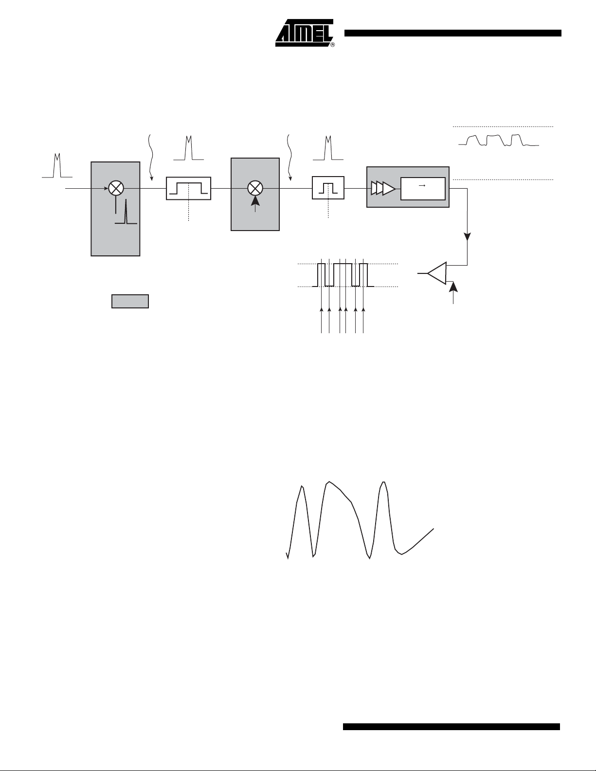
Figure 2-1. Principle of Demodulation
Signal down-converted
at 10.7 MHz
1st filtering stage 2nd filtering stage
RF
F
L01
Embedded function
bandwidth = hundreds of kHz
10.7 MHz
DATAMSG
DATACLK
nd
2 down-conversion
at 455 kHz
L02
bandwidth = tens of kHz
SYNCHRONOUS RESHAPED
Discriminator
FV
Converter
455 kHz
CMOS LEVELS
Vcc
GND
Data slicer
threshold
CLOCK RECOVERY
Vcc
GND
The AT86RF211S discriminator is analog: the output voltage is proportional to the input frequency. It was particularly designed to accept a very long sequence of “zeros” or “ones” (i.e. a
constant input frequency). This is not the case for all receivers (in other words, with some
transceivers it is necessary to use DC-free data encoding).
Figure 2-2. Classic Discriminator without DC Ability
01011010
Sequence
2
AT86RF211S Application Note
5418A–WIRE–04/05
Page 3

Figure 2-3. AT86RF211: Discriminator with DC Ability
0101101
2.1.2 Standard/Narrowband Modes of the Discriminator
Since the output swing of the discriminator is proportional to the input frequency deviation,
small frequency deviations (used in narrowband applications) lead to smaller peak-to-peak
values of discriminator output. For this reason, the discriminator’s gain can be selected. The
AT86RF211S features four different gains – NDB, SDB, MDB and WDB – where NDB and
SDB are fully compatible with the AT86RF211.
AT86RF211S Application Note
Sequence
The slope of the demodulator is:
• Standard Discriminator Bandwidth mode: 14 mV/kHz at 2.4V (+5 mV per volt of power
supply)
• Narrow Discriminator Bandwidth mode: 28 mV/kHz at 2.4V (+10 mV per volt of power
supply)
• Medium Discriminator Bandwidth mode: 9 mV/kHz at 2.4V (+4 mV per volt of power
supply)
• Wide Discriminator Bandwidth mode: 5.5 mV/kHz at 2.4V (+2 mV per volt of power supply)
2.1.3 System Requirements
In order for the system to operate properly, the basic requirements are the following:
• The frequency deviation must be in accordance with the data rate (the higher the data rate,
the larger the frequency deviation).
• The down-converted frequencies must remain within the IF filters over the entire operating
conditions (temperature range, ageing), particularly when a narrow IF2 filter is used.
The typical values are:
=> 10.7 MHz filter: ±50 to ±150 kHz (ceramic filter)
=> optional 455 kHz second IF filter: ±2 to ±17.5 kHz (ceramic filter).
• The output of the discriminator must not exceed the maximum allowed voltage range. The
level on DISCOUT depends on several parameters: the received signal frequency, the
receiver local oscillator, the amplifier offsets, etc.
Important Notes:
5418A–WIRE–04/05
• The temperature drifts of the crystal are often given in ppm (parts per million) over a given
temperature range. 1 ppm is 0.9 kHz at 900 MHz and 0.4 kHz at 400 MHz, with a 10.245
MHz crystal.
3
Page 4
2.2 Data Slicing
Figure 2-4. Data Slicing
• The crystal specifications in this document (ageing and temperature drifts) are given for the
868 to 915 MHz bands. For an application in the 400 MHz to 480 MHz band, these
specifications can be relaxed and multiplied by 2.
• These specifications (temperature and ageing) include the Tx and Rx sides: the overall drift
must meet these requirements.
• Thanks to the high resolution of the AT86RF211S synthesizer (typically 200 Hz) a given
accuracy can be achieved by software: a small shift of the frequency (made by software) is
able to compensate a temperature or ageing drift with no additional hardware cost.
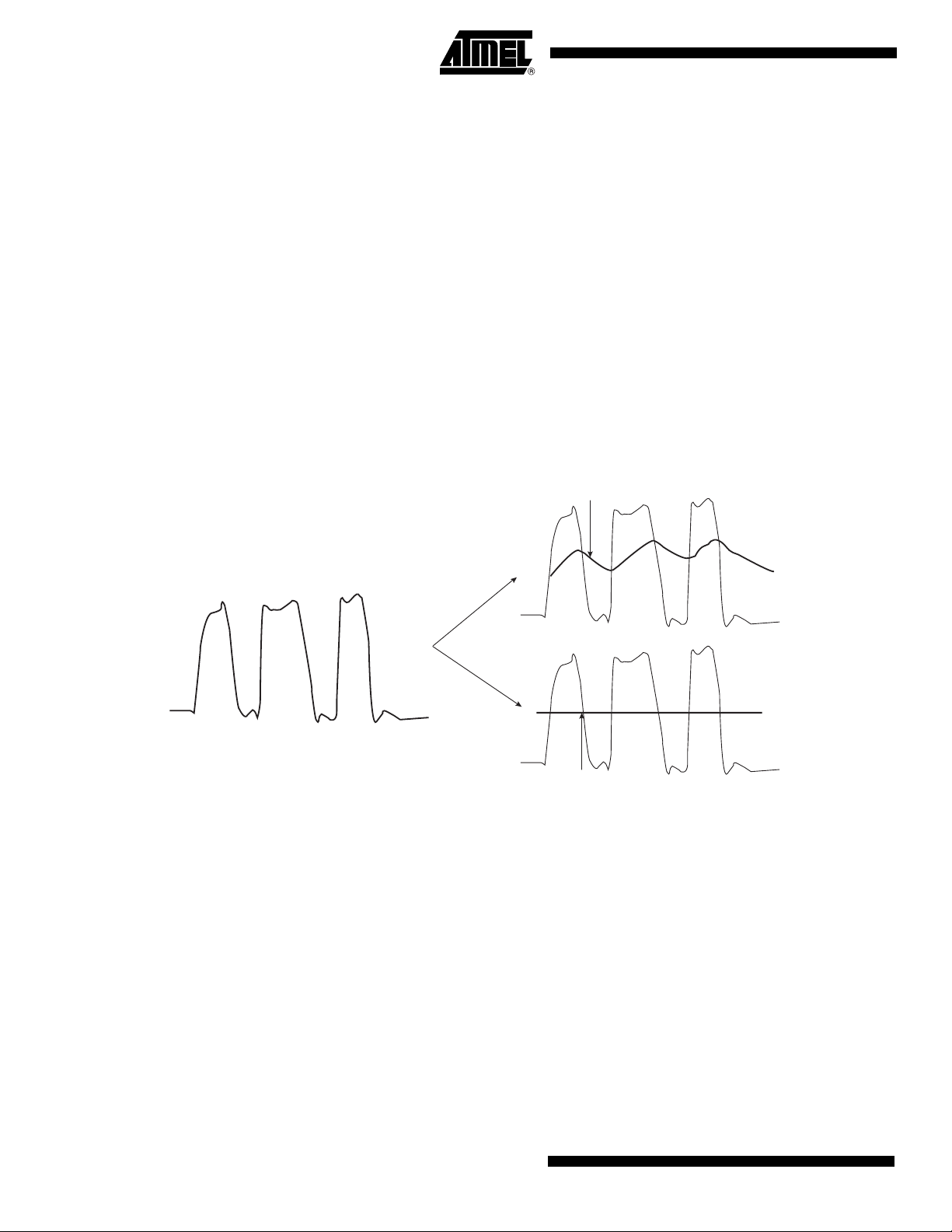
Once the frequency has been converted into a voltage, a decision must be made to identify
the “0” and “1” levels and convert them into CMOS levels. This is achieved thanks to a comparator. The AT86RF211S offers two data-slicing possibilities.
Data slicer threshold set on SKFILT pin
Data slicing
options
Demodulated signal on DISCOUT pin
Data slicer threshold level set by internal DAC (DSREF)
With the AT86RF211S, a hold is possible on the SKFILT capacitor. This helps to maintain the
average value of the signal captured without any discharge during reception of the message.
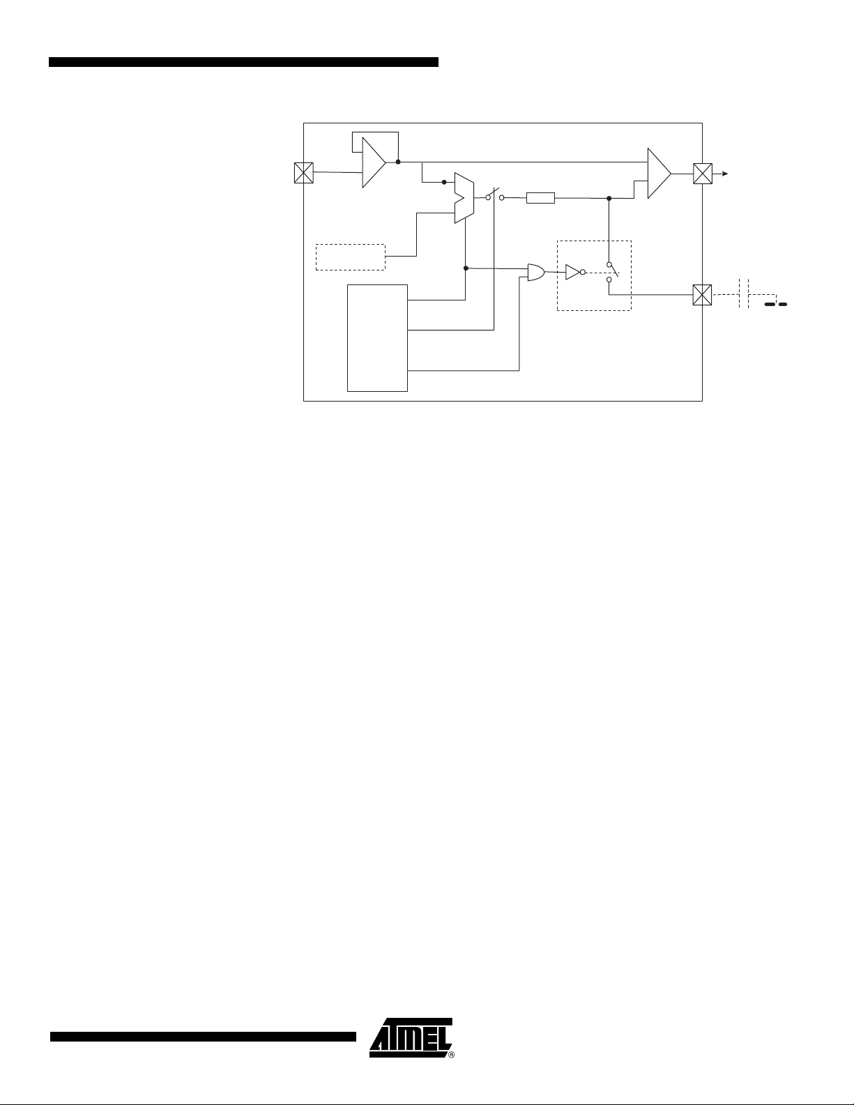
2.2.1 External Mode Comparing The Signal to its Average Value
A first possibility consists in comparing the signal to its own average value: a capacitor on
SKFILT (pin 25) is charged to the average value of the signal.
4
AT86RF211S Application Note
5418A–WIRE–04/05
Page 5
AT86RF211S Application Note
Figure 2-5. “External” Comparison Mode: Signal Compared to its Average Value.
Demodulator
Output
(DSIN)
+
-
DAC
Data Slicer
0
1
+
100K
A
-
Data Slicer
Threshold
B
DATAMSG
SKFILT
The value of the capacitor is a trade-off: it must be low enough to make the charging time as
short as possible, but high enough to “memorize” the level during the length of the maximum
number of similar consecutive bits. The lower the data rate, the higher the capacitor. Practical
values are:
• Data rate = 2400 bps => C = 22 nF
• Data rate = 4800 bps => C = 10 nF
• Data rate = 9600 bps => C = 4.7 nF
• Data rate ≥ 19200 bps => C = 2.2 nF
This procedure makes it impossible to receive a signal containing a DC component (= a long
sequence of “0” or “1”): the signal and data slicer thresholds become very close to one another
and the decision can no longer be made. Therefore, an adequate data encoding technique
must be used to prevent any DC component.
5418A–WIRE–04/05
Manchester encoding is a popular way of preventing the existence of any DC component. It
consists in encoding the data as follows:
– Logical “0”: 01
– Logical “1”: 10
This way, a long sequence of “0s” will be transformed into a “0101010101…” sequence. A
maximum of two similar successive low or high levels can be seen.
Note: Many other DC-free data encoding techniques are possible that increase the effectiveness of
the encoding, but the principle of operation is the same.
Thanks to the new “Charge & Hold” feature of the AT86RF211S, it is possible to suppress
message encoding. A dedicated application note entitled “Benefits of Charge & Hold” reference 5420, is available that details this.
5
Page 6

2.2.2 Internal Mode Comparing the Signal to a Fixed Level
A second possibility consists in comparing the signal to a fixed threshold (that does not
depend on the signal itself). This is a very powerful mode: it enables you to take advantage of
the receiver’s full bandwidth without need for a preamble (the first bit can be data sliced correctly and processed by the microcontroller).
Figure 2-6. Internal Comparison Mode: Signal Compared to a Fixed Level
+
DISCOUT
-
DATAMSG
Signal
+
-
Fixed threshold
(internally set up
by software, DTR[5:2])
+
DSIN
In this mode, the system designer must make sure that the data slicer threshold is tuned close
to the middle of the demodulated signal.
Figure 2-7. “Internal” Comparison Mode
DISCOUT:
demodulated
data
OK
Notes: 1. If an active low-pass filter with a transistor (Sallen-Key for instance) is inserted between DIS-
COUT and DSIN, the internal comparison mode must be avoided as the Vbe offsets the
demodulated signal out of the data slicer window. The use of an op. amp. does not offset
and the signal thereafter is allowed for active filtering.
2. It is recommended to use a simple R/C low-pass filter instead of an active one.
Not OK
Comparator threshold
Time
2.2.3 Manchester vs. NRZ
2.2.3.1 Manchester
• The frequency spectrum is uniform (same number of “0” and “1” frequencies).
• The demodulator can be simple (no DC level).
• Data slicing is very easy (the default threshold is at the middle of the demodulated signal).
• A preamble to charge the capacitor to a correct value is required.
• Two transitions are required to send one bit. Since the number of transitions per second is
6
AT86RF211S Application Note
limited by the hardware, the number of “useful” bits is divided by two. For instance, with 128
000 transitions per second allowed by the AT86RF211S, 64 000 useful bits can be
transmitted in this mode.
5418A–WIRE–04/05
Page 7

2.2.3.2 NRZ
AT86RF211S Application Note
• Enhanced encoding effectiveness.
• If the internal mode is used:
– there is no need for a preamble once the threshold is properly set-up (the first bit
can be demodulated).
– 128 000 transitions per second = 128 000 useful bits.
– the threshold must be tuned (this can be done automatically through the software).
• If the external mode is used:
– the Hold mode grants the data slicer long streams of ‘0’ and ‘1’.
– there is a need for a preamble to “charge” the C
SKFILT
.
3. Embedded Tools for Discriminator/Data Slicer Tuning
The AT86RF211S has all the relevant embedded tools to tune the output of the discriminator
and the data slicer threshold to meet any requirements. All these operations are carried out by
the software.
5418A–WIRE–04/05
7
Page 8

3.1 Measuring the Output of the Discriminator
The voltage on the DISCOUT pin can be read by setting CTRL1[24] = “1” and CTRL1[1] =”1”:
the result is stored into STATUS[23:18]. An unmodulated RF carrier must be at the input of the
receiver (at least 10 dB above sensitivity).
3.2 Tuning the Output Level of the Discriminator
The output voltage of the discriminator can be shifted (up or down) by setting:
• DISCHIGH (DTR[1]=”1”) adds a positive offset to the output = +220 mV + 100 mV × (V
- 2.4V) for the SDB.
• DISCLOW (DTR[0]=”1”) adds a negative offset to the output = -220 mV - 100 mV × (V
- 2.4V) for the SDB.
One obtains ±220 mV at V
For NDB, the shift is (SDB) × 2.
For MDB, the shift is (SDB) × 2/3.
For WDB, the shift is (SDB) × 2/5.
3.3 Tuning the Data Slicer Threshold
DTR[5:2] make it possible to tune the data slicer threshold around Vcc/2. 16 levels are possible
(LSB = 15 mV per Volt of supply voltage). V
reset value is 1000.
LSB’s value for usual values of power supply voltage:
• 2.4V: 36 mV
• 2.7V: 41 mV
•3V: 45 mV
• 3.3V: 50 mV
• 3.6V: 54 mV
= 2.4V and ±340 mV at Vcc = 3.6V. This is for the SDB selection.
cc
/2 corresponds to DTR[5:2] = “0111”, and the
cc
cc
cc
8
AT86RF211S Application Note
5418A–WIRE–04/05
Page 9

4. Deviations and Crystal Specifications
4.1 Overall Procedure
• Rule 1: the frequency deviation is in accordance with the data rate so that the
demodulation is operated properly.
• Rule 2: the down-converted signals (10.7 MHz, 455 kHz) remain within the IF filters over
the whole operating conditions (T° range, ageing).
• Rule 3: the output of the discriminator stays within the guaranteed range over the whole
operating conditions (T° range, ageing).
• Rule 4: the data slicer threshold must be tuned close to the middle of the demodulated
signal if the “internal” mode is used. If not, the drift compensation is naturally done thanks
to the SKFILT capacitor charge.
Note: The “internal” mode for the data slicer is not mandatory as the SKFILT capacitor can be used as
the reference level (the discriminator has the ability to demodulate CW). The user must choose
the relevant value for this capacitor to ensure that the capacitor remains charged during the
“0000...” and “1111...” sequences. In this case, it is not possible to send an infinite sequence of
“0” or “1” as with the internal mode. For instance, using C = 4.7 nF with a 9600 bps data rate
sets the limit for a correct sequence to be received to 10 similar bits.
AT86RF211S Application Note
If no encoding is used, then the “Charge & Hold” mode can be operated. It allows you to set
the SKFILT capacitor to “hold”. The average level captured during the preamble is then kept
during the entire message. An application note dedicated to this subject is available, entitled
“Benefits of Charge & Hold” reference 5420.
4.1.1 Meeting Rule No. 1
The chosen deviation must be as wide as possible to maximize sensitivity. Our recommended
minimum deviations are the following:
4.1.2 Meeting Rule No. 2
The limitation very often comes from the narrow bandwidth of the 455 kHz filter. A margin must
be considered between the total deviation and the bandwidth otherwise a distortion may
appear. For example, with a 3 dB bandwidth of ±15 kHz, it is not recommended to have a deviation wider than ±10 kHz. In addition, any ppm drift of the crystal implies a kHz drift of the
signal into the filter. Of course, thanks to the fine software tuning of the synthesizer, this can be
compensated for very easily.
• <4800 bps: ±4 kHz
• 9600 bps: ±6 kHz
• 19,200 bps: ±10 kHz
• 38,400 bps: ±19.2 kHz
• 50,000 bps: ±25 kHz
• 100,000 bps: ±50 kHz
• 128,000 bps: ±64 kHz
5418A–WIRE–04/05
9
Page 10

4.1.3 Meeting Rule No. 3
The minimum and maximum levels on DISCOUT that must not be exceeded are:
• From 0.4V to 2.2V for V
• From 0.7V to 3.5V for V
• The DC level on DISCOUT is the sum of the frequency deviation on the T
= 2.4V (total range = 1.8V)
CC
= 3.6V (total range = 2.8V)
CC
x, the crystal drifts
and to the natural DC level of the discriminator
The natural DC level of the discriminator, understood with a pure 455 kHz on IF2IN, depends
on the NDB, SDB, MDB and WDB selection but not on the temperature. The temperature drift
can be neglected – only the crystal drifts need be considered.
These parameters lead to the Equivalent Deviation Range ( = crystal drifts + deviation).
Without any DISCHIGH/DISCLOW compensation, the EDR limits are:
Equivalent Deviation
Range
Maximum Deviation Crystal Drifts
NDB ± 15 kHz ± 8 kHz ± 7 ppm
SDB ± 50 kHz ± 30 kHz ± 20 ppm
MDB ± 75 kHz ± 55 kHz ± 20 ppm
WDB ± 125 kHz ± 100 kHz ± 25 ppm
Notes: 1. As previously noted, the crystal drifts must be understood as (Rx +Tx) drifts. The deviations
can be set as expected by the user. The drifts are thereby modified in accordance with the
EDR.
2. In the 433 MHz band, the crystal drifts can be relaxed by ×2.
3. The initial tolerance of the crystal is not considered when mentioning drifts.
Example of Deviation/Drifts
(868/915 MHz Bands)
10
Use of the DISCHIGH/DISCLOW compensation is possible for all selections. However, it is
not recommended for the SDB, MDB and WDB as the natural DC level on DISCOUT is low
enough not to require any compensation. The above-described deviations and tolerances are
wide enough to enable any application requirements.
This compensation may be of interest for the NDB selection to relax constraints over crystals.
Moreover, once the DISCHIGH/DISCLOW compensation is done on the production bench,
there are no expected drifts except for those of the crystals. The EDR then becomes approximately
±19 kHz providing a relaxed crystal constraint of ±4 ppm compared to the non-compensated
one.
The DISCHIGH/DISCLOW compensation means that the best setting leading to the smallest
offset from V
/2 has been programmed.
CC
AT86RF211S Application Note
5418A–WIRE–04/05
Page 11

4.1.4 Meeting Rule No. 4
One must ensure that the demodulated data can be correctly data-sliced and reshaped. If the
''external'' mode is used, the average level of the demodulated signal is the reference of the
data slicer. There is no problem for meeting rule 4.
If the ''external'' mode is used in combination with the ''Charge & Hold” mode, the average
level of the demodulated signal is captured and kept as the reference of the data slicer. There
is no problem for meeting rule n°4.
If the ''internal'' mode is used, the reference level of the data slicer is the DAC output. Therefore, you must ensure that the demodulated signal stays in the window of the data slicer
comparator.
The “internal” level can be set on the production bench, then stored in the memory of the application module. Afterwards, the drifts to be considered and compensated for are only the drifts
of the crystals, as the discriminator offers a constant DC level over the operating temperature
range.
AT86RF211S Application Note
The LSB of the data slicer DAC is from 36 mV (at V
= 2.4V) to 54 mV (at VCC = 3.6V). The
CC
conversion gains of the discriminator can be expressed in mV/ppm (instead of mV/kHz) as
1 ppm is equivalent to 1 kHz in the 868/915 MHz bands. Therefore, whatever V
, the rule is:
CC
• NBD: 1 ppm corresponds to 0.80 × LSB
• SBD: 1 ppm corresponds to 0.40 × LSB
• MBD: 1 ppm corresponds to 0.25 × LSB
• WBD: 1 ppm corresponds to 0.15 × LSB
We recommend that the “internal” DAC level be checked and modified in accordance with the
following rule, where V
is the DSIN peak-to-peak demodulated signal and LSB is the DAC
PP
LSB corresponding to the current application:
•V
< 5 × LSB: check each time the drift corresponds to 1 × LSB
PP
•V
< 10 × LSB: check each time the drift corresponds to 2 × LSB
PP
•V
= 10 × LSB: check each time the drift corresponds to 3 × LSB
PP
The following table derives from the two afore-described rules, providing the maximum drifts
allowed between “internal” DAC corrections:
VPP < (5 × LSB) VPP < (10 × LSB) VPP > (10 × LSB)
NDB 1.5 ppm 3 ppm 4.5 ppm
SDB 2.5 ppm 5 ppm 7.5 ppm
5418A–WIRE–04/05
MDB 4 ppm 8 ppm 12 ppm
WDB 6.5 ppm 13 ppm 20 ppm
If the current application does not exceed these limits, only the production bench setting is
mandatory. If subsequent applications do exceed these limits, a compensation will be necessary (based on the temperature conditions).
11
Page 12

Examples:
SDB selection with a modulation of ±20 kHz, low data rate, operated at V
= 3V and in the
CC
868 MHz band:
The peak-to-peak signal after demodulation has a range of ±340 mV. The DAC’s LSB is
45 mV. Therefore, the voltage swing equals 15 times the LSB. A compensation of the DAC is
required if 7.5 ppm drifts are expected, whether from the Rx or Tx side, or a combination of
both. If operated in the 433 MHz band, this constraint is relaxed to a drift of 15 ppm.
WDB selection with a modulation of ±80 kHz, 100 kbps, operated at V
= 3V and in the
CC
915 MHz band:
The peak-to-peak signal after demodulation has a range of ±450 mV. Notice that at low data
rates, it would be ±550 mV but because of the F
of the discriminator, at 100 kbps, the
CUT-OFF
signal has less swing.
The DAC’s LSB is 45 mV. Therefore, the voltage swing equals 20 times the LSB. A compensation of the DAC is required if approximately 20 ppm drifts are expected, whether from the Rx
or Tx side. If operated in the 433 MHz band, this drift is relaxed to 40 ppm. This means that for
such applications, it may be that no compensation is necessary.
12
AT86RF211S Application Note
5418A–WIRE–04/05
Page 13

AT86RF211S Application Note
5. Appendix 1
5.1 Setting Up the DTR[5:2]
This appendix is relevant only if the internal data slicer mode is used.
A given sequence feeds the receiver with 010101... (50% duty cycle). The DTR[5:2] is tuned
from “0000” up to “1111”. For the lowest values, the comparator level is too low, thereafter the
DATAMSG pin is showing only “1” as the discriminator output is always below the comparator
threshold. For the highest values, the comparator level is too high thereafter the DATAMSG
pin is showing only “0” as the discriminator output is always above the comparator threshold.
The value to be chosen is the one for which the DATAMSG pin shows a correct message on
DATAMSG pin. This value is in the middle between the “last” DTR[5:2] showing only “1” at
DATAMSG pin and the “first” DTR[5:2] showing only “0” at DATAMSG pin.
The value of the DTR [5:2] register is stored in the application memory.
5.1.1 Duty Cycle Method (Internal Data Slicer Mode Only)
A given sequence feeds the receiver = 010101... (50% duty cycle). DTR[1:0] and DTR[5:2] are
tuned to have a duty cycle at the output of the data slicer as close as possible to 50%.
5418A–WIRE–04/05
13
Page 14

6. Appendix 2
6.1 AT86RF211S Relevant Registers
CTRL1[24] : MVCC: selection of the ADC mode (RSSI or Voltage)
CTRL1[6] : FSKBW: selection of the bandwidth of the discriminator
CTRL1[4] : DSREF: selection of the data slicing mode (internal or external)
CTRL1[1] : MOFFSET: measurement of level on DISCOUT pin (no modulation)
DTR [5:2] : DSREF: DAC word for reference level adjustment of data slicer threshold
DTR [1] : DISCHIGH: positive shift of the DC level on DISCOUT pin
DTR [0] : DISCLOW: negative shift of the DC level on DISCOUT pin
STATUS : MVCC: stores the word
[23:18]
Extended : CTRL1[0]=1
mode:
DTR[26:25]: : DISCRANGE – selection of the bandwidth range of the discriminator.
14
AT86RF211S Application Note
5418A–WIRE–04/05
Page 15

Atmel Corporation Atmel Operations
2325 Orchard Parkway
San Jose, CA 95131, USA
Tel: 1(408) 441-0311
Fax: 1(408) 487-2600
Regional Headquarters
Europe
Atmel Sarl
Route des Arsenaux 41
Case Postale 80
CH-1705 Fribourg
Switzerland
Tel: (41) 26-426-5555
Fax: (41) 26-426-5500
Asia
Room 1219
Chinachem Golden Plaza
77 Mody Road Tsimshatsui
East Kowloon
Hong Kong
Tel: (852) 2721-9778
Fax: (852) 2722-1369
Japan
9F, Tonetsu Shinkawa Bldg.
1-24-8 Shinkawa
Chuo-ku, Tokyo 104-0033
Japan
Tel: (81) 3-3523-3551
Fax: (81) 3-3523-7581
Memory
2325 Orchard Parkway
San Jose, CA 95131, USA
Tel: 1(408) 441-0311
Fax: 1(408) 436-4314
Microcontrollers
2325 Orchard Parkway
San Jose, CA 95131, USA
Tel: 1(408) 441-0311
Fax: 1(408) 436-4314
La Chantrerie
BP 70602
44306 Nantes Cedex 3, France
Tel: (33) 2-40-18-18-18
Fax: (33) 2-40-18-19-60
ASIC/ASSP/Smart Cards
Zone Industrielle
13106 Rousset Cedex, France
Tel: (33) 4-42-53-60-00
Fax: (33) 4-42-53-60-01
1150 East Cheyenne Mtn. Blvd.
Colorado Springs, CO 80906, USA
Tel: 1(719) 576-3300
Fax: 1(719) 540-1759
Scottish Enterprise Technology Park
Maxwell Building
East Kilbride G75 0QR, Scotland
Tel: (44) 1355-803-000
Fax: (44) 1355-242-743
RF/Automotive
Theresienstrasse 2
Postfach 3535
74025 Heilbronn, Germany
Tel: (49) 71-31-67-0
Fax: (49) 71-31-67-2340
1150 East Cheyenne Mtn. Blvd.
Colorado Springs, CO 80906, USA
Tel: 1(719) 576-3300
Fax: 1(719) 540-1759
Biometrics/Imaging/Hi-Rel MPU/
High Speed Converters/RF Datacom
Avenue de Rochepleine
BP 123
38521 Saint-Egreve Cedex, France
Tel: (33) 4-76-58-30-00
Fax: (33) 4-76-58-34-80
Literature Requests
www.atmel.com/literature
Disclaimer: The information in this document is provided in connection with Atmel products. No license, express or implied, by estoppel or otherwise, to any
intellectual property right is granted by this document or in connection with the sale of Atmel products. EXCEPT AS SET FORTH IN ATMEL’S TERMS AND CONDI-
TIONS OF SALE LOCATED ON ATMEL’S WEB SITE, ATMEL ASSUMES NO LIABILITY WHATSOEVER AND DISCLAIMS ANY EXPRESS, IMPLIED OR STATUTORY
WARRANTY RELATING TO ITS PRODUCTS INCLUDING, BUT NOT LIMITED TO, THE IMPLIED WARRANTY OF MERCHANTABILITY, FITNESS FOR A PARTICULAR
PURPOSE, OR NON-INFRINGEMENT. IN NO EVENT SHALL ATMEL BE LIABLE FOR ANY DIRECT, INDIRECT, CONSEQUENTIAL, PUNITIVE, SPECIAL OR INCIDENTAL DAMAGES (INCLUDING, WITHOUT LIMITATION, DAMAGES FOR LOSS OF PROFITS, BUSINESS INTERRUPTION, OR LOSS OF INFORMATION) ARISING OUT
OF THE USE OR INABILITY TO USE THIS DOCUMENT, EVEN IF ATMEL HAS BEEN ADVISED OF THE POSSIBILITY OF SUCH DAMAGES. Atmel makes no
representations or warranties with respect to the accuracy or completeness of the contents of this document and reserves the right to make changes to specifications
and product descriptions at any time without notice. Atmel does not make any commitment to update the information contained herein. Atmel’s products are not
intended, authorized, or warranted for use as components in applications intended to support or sustain life.
r
© Atmel Corporation 2005. All rights reserved. Atmel®, logo and combinations thereof, and Everywhere You Are® are registered trademarks,
and others are trademarks of Atmel Corporation or its subsidiaries. Other terms and product names may be trademarks of others.
Printed on recycled paper.
5418A–WIRE–04/05
xM
 Loading...