

Page 1
www.DataSheet4U.com
Features
•
850–930 MHz Output Frequency
•
Rx Current: 14.5 mA
•
Low Sleep Mode Current: 1 uA
•
DSSS Processing and BPSK Modulation/Demodulation
•
Battery Voltage Monitoring Circuitry
•
4 mW (6 dBm) Min. Transmit Power @ Vdd = 1.8V
•
Serial Peripheral Interface (SPI) Control
•
Power Supply Voltage Operating Range: 1.8V to 3.6V
•
Low External Component Count
•
48QFN Package
Applications
•
Low Band IEEE 802.15.4/ZigBee™-based Systems
•
Industrial, Commercial, Home Lighting Control, Security, and HVAC
•
Inventory Management
•
Health Monitoring
•
Wireless PC Peripherals such as Mouse, Keyboard, and Joystick
•
Consumer Electronics Remote Controls and Toys
Description
The Atmel AT86RF210 Z-Link™ Transceiver is a fully integated, low-cost ZigBee
transceiver cap able of transmitting and receiving B PSK modulated digital data over a
frequency range of 868 MHz and 902–928 MHz using a minimum number of external
components. It combines excellent RF performance with low cost, small size and low
current consumpt ion . The AT86RF210 includes a c r ystal st abilized Fractional-N s ynthesizer, BPSK transmitter and receiver, and full Direct Sequence Sp read Spectrum
Signal (DSSS) processing, including spreading and despreading. The device is fully
compatable with IEEE 802.15.4 and ZigBee standards. It includes internal voltage
regulation and battery monitoring circuitr y and requires a minimum number of external
support components.
™
AT86RF210
Z-Link
™
Transceiver
868/902–928 MHz
Direct Sequence
Spread Spectrum
BPSK Transceiver
Preliminary
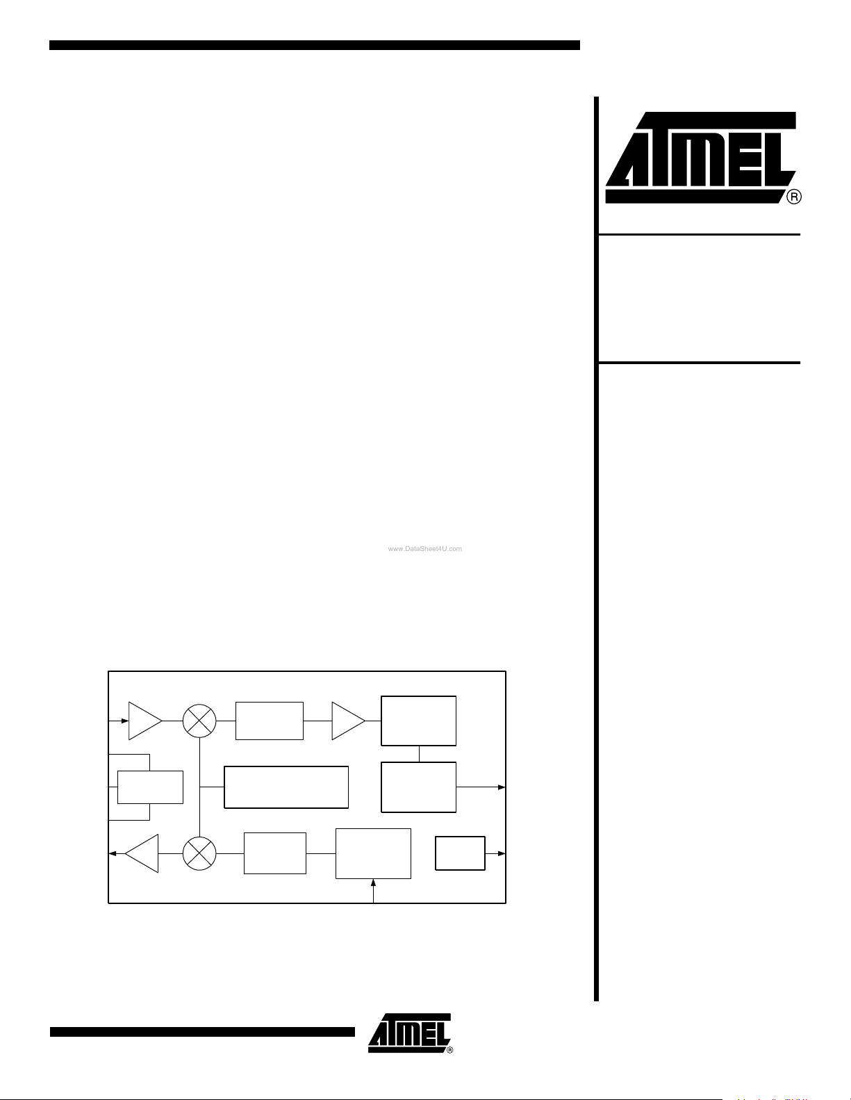
Figure 1. Block D iagram
Rx In
Sw Out
Ant In
Sw In
Tx Out
Low Noise
Amp
T/R Switch
Power Amp
I/Q Mixer
IF Amp
X
Polyphase
Filter
Synthesizer
Modulator
Demodulator
Despreader
Spreader
Data In
SPI Bus
Data Out
SDO
SDI
SCLK
SEL
5033AS–WIRE–10/03
Page 2

Figure 1. Functional Block Diagram
SUB
LNAIN
LNAVSS
RSWOUT
VSS
ANT
VSS
TSWIN
VSS
PA OUT
VSS
TR
SW
PA
Regulator
LNAOUT
LNA
PA
GND
FSK
TUNE LOGIC
Fine
Atten
BPSKO
OK
MOD
VDDA
VSSA
/2
with
Buffers
FROM TXD
Spreader
VCO
Fcx2
Cap
Array
VDDD
VSSD
Reg Filter
Lim/PPF DC DIST
Image
P
P
F
M
U
X
1
Reject
Filter
1.200 MHz
bandwidth
Control
PPF
AUTOCAL
Circuit
P
P
F
M
U
X
2
DC DIST/BG/PTAT with
main BandGAP
/N-M
SDMOD
Tune W ord
Charge
Pump
PRGM
DIV
Coarse
Lock/Lock
Detect
Phase
Detector
VDD
DBLR
RSSI
IQ-Limiter Strip
1.2 MHz
Low
Voltage
Detect
Clock
Distribution
Xstal Osc
S
T
A
T
U
S
TEST
POR
Despreader
BPSK
Demod
Mode
Logic
Serial
Configruation
Register
RXD
CCA
START
TXD
NC
CHP_RDY
RESET_
RX
TX
CLK
SEL
SCL
SDO
PAREG
VCOREG
VCO
NC
NC
VCO
VSS
VCO
TUNE
CPVCO
CPOUT
XTALGND
XTAL1
XTAL2
SDI
Table 1. Absolute Maximum Ratings*
Storage Temperature ..............................................−65 to +150
Maximum Input Voltage...........................................VDD + 0.5V
Maximum Operating Voltage (VDD ) ................................... 4,5
*NOTE: Stresses beyond those listed in this table may cause per-
manent damage to the device. This is a stress rating
only; functional operation of the device at these or any
other co ndit ions beyond thos e indic ate d in the op eration al sec t io ns of the specification is not implied.
Exposure to the absolute maximum rating conditions for
extended periods may affect device reliability.
Table 2. Operating Conditions
Symbol Parameter Min Typ Max Unit
TAMB Operating temperature −40 85 °C
VSUPPLY Voltage supply range 1.8 2.7 3.6 V
HUMIDITY Humidity 10 90 %
Note: Unit operation is guaranteed by design when operating within these ranges.
2
AT86RF210
5033AS–WIRE–10/03
Page 3
AT86RF210
Table 3. DC Characteristics
Symbol Parameter Min Typ Max Unit
IDDRX Supply current, receive mode 14.5 mA
IDDTX Supply current, transmit mode VDD = 3.3V 60 mA
IDDSleep Supply current, sleep mode 1 uA
VPOR Power-on reset voltage 1.5 V
VIH Digita l i nput voltage high 0.7*VDD V
VIL Digital i nput voltage low 0.3*VDD V
VOH Digital output voltage high 0.7*VDD V
VOL Digital output voltage low 0.3*VDD V
Table 4. Receiver AC Characteristics
Symbol Parameter Min Typ Max Unit
FLO Local oscillator opera ting range, external
inductor
ZRF Port impedance antenna input 50 Ohm
Rx Sens Sensitiv i ty, PER = 1% 4 0 kB/s, BW = 600 kHz
BPSK modulation
Rx NF Receiver noise figure 6.0 dB
Rx P1dB Receiver input 1dB compression point LNA
gain max setting
Rx IP3 Input IP3 −30 dBm
Rx LO Leakage Receiver LO leakage (all possible paths) −80 dBm
Pin Maximum input signal; LNA gain min setting −20 dBm
EDthresh Default energy detection threshold
(programmable)
Ttx/rx Turnaround time, trans mit to receive 100 usec
Trx/tx Turnaround time, receive to transmit 100 usec
RJAMadj Receiver relative jamming resistance adjacent
channel (desired signal = −89 dBm)
RJAMalt Receiv er r elativ e jam ming res istanc e alternate
channel (desired signal = −89 dBm)
IFCF IF center frequency 1.2 MHz
850 930 MHz
−95 dBm
−40 dBm
−84 dBm
0dB
30 dB
IFBW IF bandwidth 600 KHz
Imreg IF image rejection −35 dB
RX IFS/N RX IF SNR (600 KHz BW) Min input signal =
−100 dBm
Rx DR Receiver max data rate 40 Kb/s
RSSI GN RSSI Gai n 1.0 uA/dB
RSSI RG RSSI RANGE −105 −30 dBm
5033AS–WIRE–10/03
10 dB
3
Page 4

Table 5. Transmitter AC Characteristics
Symbol Parameter Min Typ Max Unit
Tx Pout Transmitter output power:
Vdd = 1.8V
Vdd = 3.6V
Rsym Tx symbol rate 915 MHz band 40 Kbit/s
Rsym Tx symbol rate 868 MHz band 20 Kbit/s
EVM Transmit error vector magnitude measured over
1000 chips
PSD Transmit power spectral density 915 MHz band;
|f–fc| >1.2 MHz (absolute measured in 100 KHz
resolution BW)
Tx Pvar Transmitter power variation over temperature 3 dB
Tx/Rx Z Antenna swi tch impedance 50 Ohm
Tx spur Transmit spurious within ±2 MHz −25 dBc
Tx spur Transmit spurious beyond ±2 MHz −35 dBc
Tx Pcon Transmitter power control resolution 0.25 0.75 dB
Tx Pran Transmitter power control range 25 dB
Tx lvt Transmitter low-voltage threshold 1.8 1.9 Volt
Tx lvpo Transmitter low-voltage output power 0.25 0.50 mwatt
Tx tot Transmitter turn-on time 90% full power 10 usec
6
12
35%
−20 dBm
dBm
Tx tofft Transmitter turn-off time less than 10% of output
power
10 usec
Table 6. Synthesizer AC Characteristics
Symbol Parameter Min Typ Max Unit
F LO Carrier frequency 850 930 MHz
LOPN LO phase noise (integrated 10 Hz–100 KHz rms) 6 deg
Fpull Crystal oscillator frequency pulli ng @ 25°C 20 ppm
Lopno Local oscillator phase noise 2.0 MHz offset from LO −95 dBc
TXtal Crystal oscillator settling time 150 usec
TSynth Phase locked loop settling time 100 usec
Synthres Synthesizer tuning resolution 500 Hz
.
Table 7. Serial Configuration Register*
Symbol Parameter Min Typ Max Unit
TRISE CMOS input rise time 20 nsec
TFALL CMOS input fall time 20 nsec
TCLKS CLK setup time 25 nsec
4
AT86RF210
5033AS–WIRE–10/03
Page 5

AT86RF210
Table 7. Serial Configuration Register* (Continued)
Symbol Parameter Min Typ Max Unit
TCLKH CLK hold time 25 nsec
TCLKW CLK pulse width 50 nsec
TSDIS SDI setup time 25 nsec
TSDIH SDI hold time 25 nsec
TSDOD SDO delay time 25 nsec
Note: *Rise and fall time is measured 10%–90%. Delay, setup, and hold times are measured 50%–50%
Table 8. Low Battery Detector Characteristics
Symbol Parameter Min Typ Max Unit
Lvbat 0 Low voltage battery detector threshold voltage mode
0 (5 bit resolution)
1.5 3.5 Volt
Table 9. Preliminary PIN Description QFN48
Startup
PIN Num Type
SUB 1 V_I/O GND Substrate connection
LNARFIN 2 RF_I NA Low-noise amplifier RF input
LNAVSS 3 RF_I/O NA Analog ground for the LNA
RSWOUT 4 RF_I/O NA Transmit- re c ei ve switc h out . Signal fr o m AN T is routed through the
VSS 5 R F_I/O NA Transmit-receive switch isolation ground 1.
ANT 6 RF_I/O NA Antenna RF input/output. Nominal impedance 50Ω, part of T/R
VSS 7 R F_I/O NA Transmit-receive switch isolation ground 2.
TSWIN 8 RF_I/O NA Transmit-receive switch input. Signal from PA comes into TR switch
PAOUT 9 RF_I/O NA PA signal routed into the T/R switch from the PA.
VSS 10 Pin not used
Cond Description
TR switch to the LNA input.
switch. R o u te s signal t o th e LN A or fro m the PA.
and is routed to ANT.
VDDA 11 V_I NA Secondary analog power supp ly input. Set in proximity to power
amplifier circuits.
PAREG 12 A_O NA PA regulator ou tput. Settable cu rrent source output for charging a
large external capacitor during battery operation.
VCOVDD 13 V_I NA VCO power supply input
VCOREG 14 V_I NA External filter cap for the VCO regulator
No Connect 15 NA Pin not used
No Connect 16 NA Pin not used
VCOVSS 17 A_I/O NA VCO power supply ground
VCOTUNE 18 A_I NA LO VCO control input. An internal di ff erent ial varactor diode tunes the
LO frequency. The control voltage should be referenced to LOGND.
5033AS–WIRE–10/03
5
Page 6

Table 9. Preliminary PIN Description QFN48 (Continued)
Startup
PIN Num Type
CPOUT 19 A_I NA Charge pump output
CPVSS 20 A_I/O NA Analog synthesizer ground
CPVDD 21 V_I NA Analog synthesizer power supply
XTAL1 22 A_I NA Crystal oscillator input 1. One side of oscillator crystal is connected
XTAL2 23 A_I NA Crystal oscillator input 2. When internal oscillator is used, this pin
XTALVSS 24 A_I/O NA Crystal oscilla tor ground
TXDAT 25 D_I HIGH Tr ansmit data input from the controller
No Connect 26 D_I LOW Pin not used
SDI 27 D_I NA Serial data input
SDO 28 D_O NA Output from configuration data shift register. Data changes at the
SCLK 29 D_I NA Serial data clock
Cond Description
to this pin.
has crystal conne cted. When external clock is used, the external
clock is input on this pin.
Input to configuration data shift register. Data accepted at the rising
edge of SCL.
falling edge of SCL.
SEL 30 D_I HIGH SPI slave select line
SYSCLK 31 D_O HIGH Cl ock output to controller. Can be divided by 1 to 16 .
TX 32 D_I HIGH Mode control input. TX HIGH with RX LOW causes chip to go to
transmit.
RX 33 D_I HIGH Mode control input. RX HIGH with TX LOW causes chip to go to
receive mode.
VDDDIG 34 V_I NA Digital power supply input
VSSDIG 35 V_I/O NA Digital power supply ground.
START 36 D_I HIGH Oscillator start. A transition on this pin will start the internal oscillato r.
A low on this pin allows the part to run from an external clock.
CHPRDY 37 D_O LOW Chip ready. Handshake signal between the controller and the chip.
Also acts as fault interrupt.
RXDOUT 38 D_O NA Digital da ta from demodulator
No Connect 39 NA Pin not used
No Connect 40 NA Pin not used
No Connect 41 Pin not used
PPFREG 42 V_I /O VD D Filter cap fo r internal low d ropout regulator for poly phase filter
RSSI 43 A_0 Logarithmic detection current
XTALMODE 44 D_IO TBD Test pin. Enables nand tree test or scan test.
CCA 45 D_O LOW Clear channel assessment. Digital signal i ndicates when channel
activity is above a programmable threshold.
6
AT86RF210
5033AS–WIRE–10/03
Page 7

AT86RF210
Table 9. Preliminary PIN Description QFN48 (Continued)
Startup
PIN Num Type
VDDA 46 V_I NA Analog (RF) power supply input
VSSA 47 V_I/O GND Analog (RF) power supply ground
LNAOUT 48 A_I/O LNA external inductor. Collector inductor for LNA. P/O RF tuning
Cond Description
network.
I/O Table Notes
• RF_I RF input
• RF_I/O RF input/output
• Voltage_I/O Voltage input/output
• V_I Voltage input
• A_I Analog input
• A_O Analog output
• D_I Digital input
• D_O Digital output
5033AS–WIRE–10/03
7
Page 8

Figure 2. Typical ZigBee Application Schematic
This is a sample application schematic for RF210
(The pinout and component values are preliminary)
Receiver T uning
C10
TBDL0TBD
Receiver Matching
L1
C17
TBD
TBD
C15
TBD
C18
100P
PA Matching
C19
TBD
L2
C22
TBD
100p
TBD
L6
X
TBD
C21
C20
250u
Optional
Note: With pin 44 (Xstal_Sel) low RF210 uses system clock from controller
With pin 44 (Xstal_Sel) high RF210 uses external crystal placed across pin 22 & 23
1 SUB
2 LNARFIN
3 LNAVSS
4 RSWOUT
5 VSS
6 ANT
7 VSS
8 TSWIN
9 PAOUT
10 VSS
11 VDDA
12 PAREG
C9
100pC810n
C14
C13
100p
10n
UT
48 LNAO
TERFACE)
(RF IN
VDD
13 VCO
R0
TBD
45 CCA
47 VSSA
46 VDDA
(DIGITAL INTERFACE)
AT86RF210
Z-Link T ransceiver
(FREQUENCY GENERATION INTERFACES)
REG
16 No connect
15 No connect
14 VCO
X
X
R2
C7
TBD
TBD
C6
TBD
Loop Filter
DE
O
44 XTALM
VSS
17 VCO
C5
TBD
C23
10n
43 RSSI
TUNE
18 VCO
100p
42 PPFREG
UT
19 CPO
C4
TBD
R1
TBD
C2
X
X
onnect
o Connect
39 N
40 No C
41 No Connect
PVSS
20 C
22 XTAL1
21 CPVDD
C3
10n
UT
38 RXDO
23 XTAL2
HPRDY
37 C
36 START
35 VSSDIG
34 VDDDIG
33 RX
32 TX
31 SYSCLK
30 SELl
ITAL INTERFACE)
29 SCLK
(DIG
28 SDO
27 SDI
26 No connect
25 TXDA T
24 XTALVSS
V_BAT
VDD
C1
100pC010n
CCA_IN
RSSI_ANALOG
START
X
RX_DATA
x
x
CHP_RDY
RX
TX
SPI_SEL
SPI_CLK
SPI_OUT
SPI_IN
TX_DAT_P
SYS_CLK_OUT
X
Atmel RF Design
Z-Link ZigBee Controller
VSS
Cent.
9/9/03
8
AT86RF210
5033AS–WIRE–10/03
Page 9

Package Drawing
48QFN
AT86RF210
Index Area
Pin 1
D
A3
A
E
A1A2
Top View
Side View
L
COMMON DIMENSIONS
(Unit of Measure = mm)
SYMBOL
D2
E2
b
e
Bottom View
D 7.00 BSC
E 7.00 BSC
D2 2.25 4.70 5.25
E2 2.25 4.70 5.25
A 0.80 0.90 1.00
A1 0.0 0.02 0.05
A2 0.0 0.65 1.00
A3 0.20 REF
L 0.30 0.40 0.50
e 0.50 BSC
b 0.18 0.23 0.30 2
MIN
NOM
MAX
NOTE
Notes: 1. This drawing is for general information only. Refer to JEDEC Drawing MO-220, Variation VKKD-2, for proper dimensions,
2325 Orchard Parkway
R
San Jose, CA 95131
5033AS–WIRE–10/03
tolerances, datums, etc.
2. Dimension b applies to metallized terminal and is measured between 0.15 mm and 0.30 mm from the terminal tip. If the
terminal has the optional radius on the other end of the terminal, the dimension should not be measured in that radius area.
TITLE
48QN1, 48-lead 7.0 x 7.0 mm Body, 0.50 mm Pitch, Quad Flat
No Lead Package (QFN)
DRAWING NO.
48QN1
12/10/02
REV.
A
9
Page 10

Atmel Corporation Atmel Operations
2325 Orchard Park way
San Jose, CA 951 31, USA
Tel: 1(408) 4 41-0311
Fax: 1(408) 487-260 0
Regional Headquarters
Europe
Atmel Sa rl
Route des Arsenaux 4 1
Case Postale 8 0
CH-1705 Fri bour g
Switzerland
Tel: (41) 26-4 26-55 55
Fax: (41) 26 -426-550 0
Asia
Room 121 9
Chinachem Golden Pla za
77 Mody Road Tsimshatsui
East Kowloon
Hong Kong
Tel: (852) 27 21-9778
Fax: (852) 2 722-136 9
Japan
9F, Tonet su Shi nkawa B ldg.
1-24-8 Shi nkawa
Chuo-ku, Tok yo 104-003 3
Japan
Tel: (81) 3-35 23-35 51
Fax: (81) 3-3 523-758 1
Memory
2325 Orch ard Par kway
San Jose, CA 95 131, U SA
Tel: 1(408 ) 441-031 1
Fax: 1(408) 43 6-43 14
Microcontrollers
2325 Orch ard Par kway
San Jose, CA 95 131, U SA
Tel: 1(408 ) 441-031 1
Fax: 1(408) 43 6-43 14
La Chantrer ie
BP 70602
44306 Nantes C ede x 3, Fra nce
Tel: (33) 2-4 0-18 -18-18
Fax: (33) 2-40-18-19-60
ASIC/ASSP/Smart Cards
Zone In dustrielle
13106 Ro usset Ced ex, France
Tel: (33) 4-4 2-53 -60-00
Fax: (33) 4-42-53-60-01
1150 East C hey enne M tn. Bl vd.
Colorado Sp rings, C O 8090 6, US A
Tel: 1(719 ) 576-330 0
Fax: 1(719) 54 0-17 59
Scottish Ent erpr ise Te chnology P ark
Maxwell Building
East Kilbrid e G7 5 0QR, Scotland
Tel: (44) 13 55-803- 000
Fax: (44) 1 355 -242-743
RF/Automotive
Theresienst rasse 2
Postfach 3535
74025 Heilbr onn, Germa ny
Tel: (49) 71-31-67-0
Fax: (49) 71 -31- 67 -2340
1150 East Ch eyen ne Mt n. B lvd.
Colorado Spring s, CO 80906, USA
Tel: 1(719) 57 6-3300
Fax: 1(719) 540 -1 759
Biometrics/Imaging/Hi-Re l MP U/
High Speed Converters/RF Datacom
Avenue de Roch epleine
BP 123
38521 Saint- Egreve Cedex, Fra nce
Tel: (33) 4-76-58-30-00
Fax: (33) 4-7 6- 58-3 4- 80
Literature Requests
www.atmel.com/literature
Disclaimer: Atmel Corporation makes no warranty for the use of its products, other than those expressly contained in the Company’s stan d a rd
warranty which is detailed in Atmel’s Terms and Conditions located on the Company’s web sit e. The Co mp any a ssu me s no resp on si bility for any
errors which may appear in this document, reserves the right to change devices or specifications detailed herein at any time without noti ce, and
does no t make any com mitment to u pdate the informat ion contai ned herei n. No license s to patents or other int ellectu al proper ty of Atmel are
granted by the C om pany in co nn ecti on wit h th e sa le of Atm el p rod ucts, expr essl y or by imp li catio n. A tme l’s products are not authorized for use
as critical components in life support devices or systems.
© Atm el Corporati on 2003. All rights reserved. Atmel® and combinations thereof are registered trademarks and Z-Link™ is a trad emark of
Atmel Corporation or its subsidiaries. ZigBee
others.
™
is a trademark of th e Zig Bee Al li ance. Othe r ter ms an d prod uct name s m ay be th e tradem ar ks of
Printe d on rec ycled pape r.
5033AS–WIRE–10/03
 Loading...