


查询AT80C51SND1C-7HTIL供应商
1. Features
• MPEG I/II-Layer 3 Hardwired Decoder
– Stand-alone MP3 Decoder
– 48, 44.1, 32, 24, 22.05, 16 kHz Sampling Frequency
– Separated Digital Volume Control on Left and Right Channels (Software Control
using 31 Steps)
– Bass, Medium, and Treble Control (31 Steps)
– Bass Boost Sound Effect
– Ancillary Data Extraction
– CRC Error and MPEG Frame Synchronization Indicators
• Programmable Audio Output for Interfacing with Common Audio DAC
– PCM Format Compatible
–I2S Format Compatible
• 8-bit MCU C51 Core Based (F
• 2304 Bytes of Internal RAM
• 64K Bytes of Code Memory
– AT89C51SND1C: Flash (100K Erase/Write Cycles)
– AT83SND1C: ROM
• 4K Bytes of Boot Flash Memory (AT89C51SND1C)
– ISP: Download from USB (standard) or UART (option)
• External Code Memory
– AT80C51SND1C: ROMless
• USB Rev 1.1 Controller
– Full Speed Data Transmission
• Built-in PLL
– MP3 Audio Clocks
–USB Clock
• MultiMedia Card
• Atmel DataFlash
• IDE/ATAPI Interface
• 2 Channels 10-bit ADC, 8 kHz (8-true bit)
– Battery V ol tage Monitoring
– Voice Recording Controlled by Software
• Up to 44 Bits of General-purpose I/Os
– 4-bit Interrupt Keyboard Port for a 4 x n Matrix
–SmartMedia® Software Interface
• 2 Standard 16-bit Timers/Counters
• Hardware Watchdog Timer
• Standard Full Duplex UART with Baud Rate Generator
• Two Wire Master and Slave Modes Controller
• SPI Master and Slave Modes Controller
• Power Management
– Power-on Reset
– Software Programmable MCU Clock
– Idle Mode, Power-down Mode
• Operating Conditions:
–3V, ±10%, 25 mA Typical Operating at 25°C
– Temperature Range: -40°C to +85 °C
• Packages
– TQFP80, BGA81, PLCC84 (Development Board)
–Dice
®
Interface Compatibility
®
SPI Interface Compatibility
= 20 MHz)
MAX
Single-Chip
Flash
Microcontroller
with MP3
Decoder and
Human Interface
AT83SND1C
AT89C51SND1C
AT80C51SND1C
Rev. 4109H–8051–01/05
AT8xC51SND1C
2. Description The AT8xC51SND1C a re fully in tegrated sta nd-alone har dwired MPEG I/II-Layer 3
decoder with a C51 microcontroller core handling data flow and MP3-player control.
The AT89C51SND1C includes 64K Bytes of Flash memory and allows In-System Pro-
gramming through an embedded 4K Bytes of Boot Flash memory.
The AT83SND1C includes 64K Bytes of ROM memory.
The AT80C51SND1C does not include any code memory.
The AT8xC51SND1C include 2304 Bytes of RAM memory.
The AT8xC51SND1C provides the necessary features for human interface like timers,
keyboard port, serial or parallel interface (USB, TWI, SPI, IDE), ADC input, I
and all external memory interface (NAND or NOR Flash, SmartMedia, MultiMedia,
DataFlash cards).
3. Typical
Applications
•MP3-Player
• PDA, Camera, Mobile Phone MP3
• Car Audio/Multimedia MP3
• Home Audio/Multimedia MP3
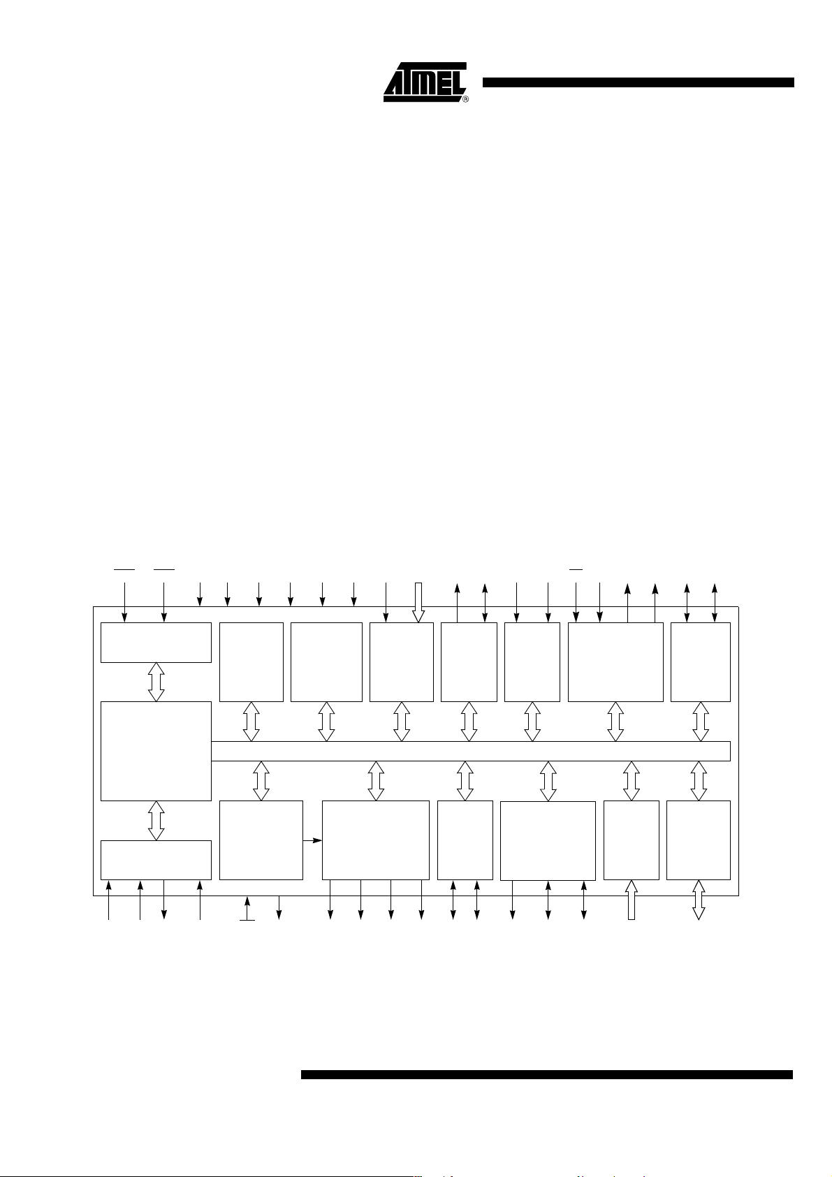
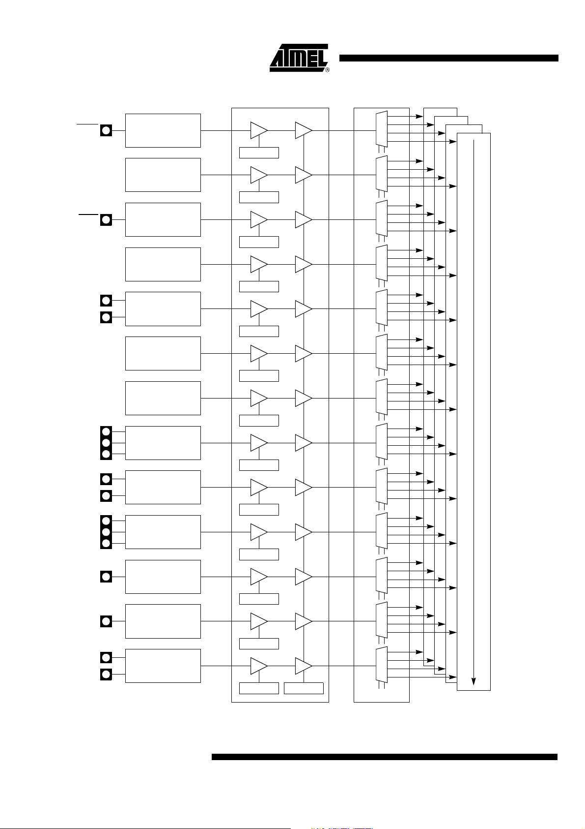
4. Block Diagram
Figure 1. AT8xC51SND1C Block Diagram
INT0 INT1 MOSIMISO
33
Interrupt
Handler Unit
VSSVDD
RAM
2304 Bytes
UVSSUVDD
AVSSAVDD
Flash
ROM
64 KBytes
Flash Boot
4 KBytes
AIN1:0
AREF
10-bit A to D
Converter
2
S output,
SCK
RXDTXD
33 33444411
UART
and
BRG
T1T0
Timers 0/1
Watchdog
SS
SPI/DataFlash
Controller
SCL SDA
TWI
Controller
C51 (X2 Core)
Clock and PLL
Unit
FILT X2X1
RST
MP3 Decoder
Unit
ISP
ALE
Audio Interface
8-Bit Internal Bus
I2S/PCM
DSELDCLK SCLKDOUT
USB
Controller
D+ D-
MCLK
MMC
Interface
MDAT
MCMD
Keyboard
Interface
1
KIN3:0
I/O
Ports
IDE
Interface
P0-P5
1 Alternate function of Port 1
3 Alternate function of Port 3
4 Alternate function of Port 4
2
4109H–8051–01/05
5. Pin Description
0
1
2
4
3
5
5.1 Pinouts
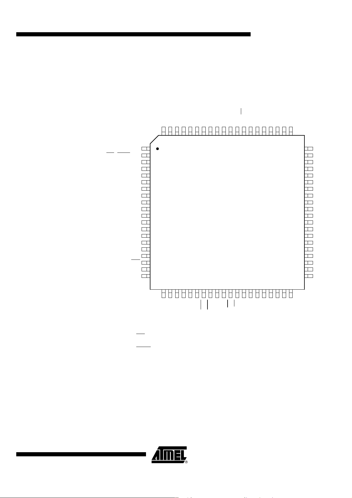
Figure 1. AT8xC51SND1C 80-pin QFP Package
ALE
1
/PSEN2/NC
ISP
P1.0/KIN0
P1.1/KIN1
P1.2/KIN2
P1.3/KIN3
P1.4
P1.5
P1.6/SCL
P1.7/SDA
VDD
PVDD
FILT
PVSS
VSS
X2
X1
TST
UVDD
UVSS
1
2
3
4
5
6
7
8
9
10
11
12
13
14
15
16
17
18
19
20
P0.3/AD3
P0.4/AD4
P0.5/AD5
VSS
VDD
717069
72
P0.6/AD6
P5.1
80
P5.0
79
P0.0/AD0
78
P0.1/AD1
77
P0.2/AD2
76
75
74
73
AT89C51SND1C-RO (FLASH)
AT83SND1C-RO (ROM)
AT80C51SND1C-RO (ROMLESS)
AT8xC51SND1C
P0.7/AD7
P4.3/SS
P4.2/SCK
67
68
P4.1/MOSI
66
P4.0/MISO
65
P2.0/A8
64
P2.1/A9
63
P4.7
62
P4.6
61
60
59
58
57
56
55
54
53
52
51
50
49
48
47
46
45
44
43
42
41
P4.5
P4.4
P2.2/A1
P2.3/A1
P2.4/A1
P2.5/A1
P2.6/A1
P2.7/A1
VSS
VDD
MCLK
MDAT
MCMD
RST
SCLK
DSEL
DCLK
DOUT
VSS
VDD
4109H–8051–01/05
21222324252627
D-
D+
VSS
VDD
P3.0/RXD
Notes: 1. ISP pin is only available in AT89C51SND1C product.
Do not connect this pin on AT83SND1C product.
2. PSEN pin is only available in AT80C51SND1C product.
28
302932
P3.4/T0
P3.3/INT1
P3.5/T1
P3.1/TXD
P3.2/INT0
31
P3.6/WR
33
34353637383940
AVSS
AVDD
P3.7/RD
P5.3
P5.2
AIN1
AIN0
AREFP
AREFN
3

AT8xC51SND1C
Figure 2. AT8xC51SND1C 81-pin BGA Package
C
B
A
D
E
F
G
H
J
P4.6
P4.4
P2.5/
A13
P2.4/
A12
VDD
RST
DSEL
DCLK
89765432
P2.0/
P4.7
P2.2/
P2.6/
A14
P2.3/
A11
MCMD
SCLK
VSS
P4.0/
MISO SCK AD2
P4.1/
MOSI
P2.1/
A9A10
P4.5
VSS
MCLK
DOUT
AIN1
P4.2/
P4.3/
SS
P0.6
P0.7/
AD7 AD5
P2.7/
A15
MDAT
P5.3
AVSS
VDD
P0.1/
VSS
P0.5/
AVDD
P3.7/
AIN0
RD
P0.2/
P0.4/
AD4 AD0AD1
P5.1
P1.6/
SCL SDA
FILT
P3.4/
T0
P3.5/
T1
P3.3/
INT1
P0.3/
AD3A8
P0.0/
P1.0/
KIN0
P1.7/
PVDD
UVSS
VDD
P3.1/
TXD
P5.0
ISP
PSEN
NC
P1.3/
KIN3
P1.5
X1
PVSS
TST
D-
1
ALE
1
/
2
P1.1
P1.2/
KIN2
P1.4
VDD
X2
VSS
UVDD
VDD
P5.2
AREFP
AREFN
P3.6/
WR
P3.2/
INT0
P3.0/
RXD
Notes: 1. ISP pin is only available in AT89C51SND1C product.
Do not connect this pin on AT83SND1C and AT80C51SND1C product.
2. PSEN
pin is only available in AT80C51SND1C product.
VSS
D+
4
4109H–8051–01/05
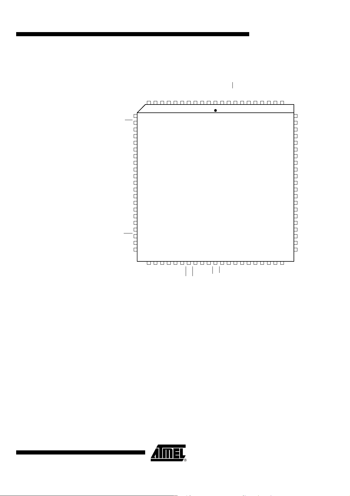
Figure 3. AT8xC51SND1C 84-pin PLCC Package
AT8xC51SND1C
ALE
ISP
P1.0/KIN0
P1.1/KIN1
P1.2/KIN2
P1.3/KIN3
P1.4
P1.5
P1.6/SCL
P1.7/SDA
VDD
PAVDD
FILT
PAVSS
VSS
X2
NC
X1
TST
UVDD
UVSS
NC
11
12
13
14
15
16
17
18
19
20
21
22
23
24
25
26
27
28
29
30
31
32
3334353637
P5.1
10
P0.3/AD3
P0.4/AD4
P0.5/AD5
VSS
VDD
P0.2/AD2
P0.1/AD1
P5.0
P0.0/AD0
432
5
6
7
8
9
P0.6/AD6
1
84838281807978
AT89C51SND1C-SR (FLASH)
3839404142
43
444546474849505152
P4.3/SS
P0.7/AD7
P4.2/SCK
P2.0/A8
P4.0/MISO
P2.1/A9
77
P4.7
76
P4.6
75
53
NC
74
73
P4.5
7271P4.4
P2.2/A10
70
P2.3/A11
69
P2.4/A12
68
P2.5/A13
67
P2.6/A14
66
P2.7/A15
65
VSS
64
VDD
MCLK
63
MDAT
62
MCMD
61
60
RST
59
SCLK
58
DSEL
57
DCLK
56
DOUT
55
VSS
54
VDD
P4.1/MOSI
D+
D-
VSS
VDD
P3.4/T0
P3.5/T1
P3.0/RXD
P3.1/TXD
P3.3/INT1
P3.2/INT0
P3.6/WR
P3.7/RD
AVSS
AVDD
AREFP
AIN1
AIN0
AREFN
NC
P5.2
P5.3
4109H–8051–01/05
5

AT8xC51SND1C
5.2 Signals All the AT8xC51SND1C signals are detailed by functionality in Table 3 to Table 16.
Table 3. Ports Signal Description
Signal
Name Type Description
Port 0
P0.7:0 I/O
P1.7:0 I/O
P2.7:0 I/O
P3.7:0 I/O
P4.7:0 I/O
P0 is an 8-bit open-drain bidirectional I/O port. Port 0 pins that have 1s
written to them float and can be used as high impedance inputs. To
avoid any parasitic current consumption, floating P0 inputs must be
polarized to V
Port 1
P1 is an 8-bit bidirectional I/O port with internal pull-ups.
Port 2
P2 is an 8-bit bidirectional I/O port with internal pull-ups.
Port 3
P3 is an 8-bit bidirectional I/O port with internal pull-ups.
Port 4
P4 is an 8-bit bidirectional I/O port with internal pull-ups.
DD
Alternate
Function
AD7:0
or VSS.
KIN3:0
SCL
SDA
A15:8
RXD
TXD
INT0
INT1
T0
T1
WR
RD
MISO
MOSI
SCK
SS
P5.3:0 I/O
Port 5
P5 is a 4-bit bidirectional I/O port with internal pull-ups.
Table 4. Cloc k Si gna l Desc r ipt ion
Signal
Name Type Description
Input to the on-chip inverting oscillator amplifier
X1 I
X2 O
FILT I
To use the internal oscillator, a crystal/resonator circuit is connected to
this pin. If an external oscillator is used, its output is connected to this
pin. X1 is the clock source for internal timing.
Output of the on-chip inverting oscillator amplifier
To use the internal oscillator, a crystal/resonator circuit is connected to
this pin. If an external oscillator is used, leave X2 unconnected.
PLL Low Pass Filter input
FILT receives the RC network of the PLL low pass filter.
-
Alternate
Function
-
-
-
6
4109H–8051–01/05
Table 5. Timer 0 and Timer 1 Signal Description
AT8xC51SND1C
Signal
Name Type Description
Timer 0 Gate Input
serves as external run control for timer 0, when selected by
INT0
GATE0 bit in TCON register.
INT0
INT1
T0 I
T1 I
I
External Interrupt 0
input sets IE0 in the TCON register. If bit IT0 in this register is set,
INT0
bit IE0 is set by a falling edge on INT0
by a low level on INT0
Timer 1 Gate Input
serves as external run control for timer 1, when selected by
INT1
GATE1 bit in TCON register.
I
External Interrupt 1
INT1
input sets IE1 in the TCON register. If bit IT1 in this register is set,
bit IE1 is set by a falling edge on INT1
by a low level on INT1
Timer 0 External Clock Input
When timer 0 operates as a counter, a falling edge on the T0 pin
increments the count.
Timer 1 External Clock Input
When timer 1 operates as a counter, a falling edge on the T1 pin
increments the count.
.
.
Table 6. Audio Interface Signal Description
Alternate
Function
P3.2
. If bit IT0 is cleared, bit IE0 is set
P3.3
. If bit IT1 is cleared, bit IE1 is set
P3.4
P3.5
Signal
Name Type Description
DCLK O DAC Data Bit Clock -
DOUT O DAC Audio Data -
DSEL O
SCLK O
DAC Channel Select Signal
DSEL is the sample rate clock output.
DAC System Clock
SCLK is the oversampling clock synchronized to the digital audio data
(DOUT) and the channel selection signal (DSEL).
Table 7. USB Controller Signal Description
Signal
Name Type Description
D+ I/O
D- I/O USB Negative Data Upstream Port -
USB Positive Data Upstream Port
This pin requires an external 1.5 KΩ pull-up to V
operation.
for full speed
DD
Alternate
Function
-
-
Alternate
Function
-
4109H–8051–01/05
7

AT8xC51SND1C
Table 8. MutiMediaCard Interface Signal Description
Signal
Name Type Description
MCLK O
MCMD I/O
MDAT I/O
MMC Clock output
Data or command clock transfer.
MMC Command line
Bidirectional command channel used for card initialization and data
transfer commands. To avoid any parasitic current consumption,
unused MCMD input must be polarized to V
MMC Data line
Bidirectional data channel. To avoid any parasitic current consumption,
unused MDAT input must be polarized to V
Table 9. UART Signal Description
Signal
Name Type Description
Receive Serial Data
RXD I/O
TXD O
RXD sends and receives data in serial I/O mode 0 and receives data in
serial I/O modes 1, 2 and 3.
Transmit Serial Data
TXD outputs the shift clock in serial I/O mode 0 and transmits data in
serial I/O modes 1, 2 and 3.
DD
or VSS.
DD
Alternate
Function
-
-
or VSS.
-
Alternate
Function
P3.0
P3.1
Table 10. SPI Controller Signal Description
Signal
Name Type Description
MISO I/O
MOSI I/O
SCK I/O
SS
SPI Master Input Slave Output Data Line
When in master mode, MISO receives data from the slave peripheral.
When in slave mode, MISO outputs data to the master controller.
SPI Master Output Slave Input Data Line
When in master mode, MOSI outputs data to the slave peripheral.
When in slave mode, MOSI receives data from the master controller.
SPI Clock Line
When in master mode, SCK outputs clock to the slave peripheral. When
in slave mode, SCK receives clock from the master controller.
SPI Slave Select Line
I
When in controlled slave mode, SS
Table 11. TWI Controller Signal Description
Signal
Name Type Description
TWI Serial Clock
SCL I/O
When TWI controller is in master mode, SCL outputs the serial clock to
the slave peripherals. When TWI controller is in slave mode, SCL
receives clock from the master controller.
enables the slave mode.
Alternate
Function
P4.0
P4.1
P4.2
P4.3
Alternate
Function
P1.6
8
SDA I/O
TWI Serial Data
SDA is the bidirectional Two Wire data line.
P1.7
4109H–8051–01/05
Table 12. A/D Converter Signal Description
AT8xC51SND1C
Signal
Name Type Description
AIN1:0 I A/D Converter Analog Inputs -
AREFP I Analog Positive Voltage Reference Input -
AREFN I
Analog Negative Voltage Reference Input
This pin is internally connected to AVSS.
Table 13. Keypad Interface Signal Description
Signal
Name Type Description
KIN3:0 I
Keypad Input Lines
Holding one of these pins high or low for 24 oscillator periods triggers a
keypad interrupt.
Table 14. External Access Signal Description
Signal
Name Type Description
Address Lines
A15:8 I/O
Upper address lines for the external bus.
Multiplexed higher address and data lines for the IDE interface.
Alternate
Function
-
Alternate
Function
P1.3:0
Alternate
Function
P2.7:0
AD7:0 I/O
ALE O
PSEN
ISP
RD
WR
(1)(2)
EA
Address/Data Lines
Multiplexed lower address and data lines for the external memory or the
IDE interface.
Address Latch Enable Output
ALE signals the start of an external bus cycle and indicates that valid
address information is available on lines A7:0. An external latch is used
to demultiplex the address from address/data bus.
Program Store Enable Output (AT80C51SND1C Only)
I/O
This signal is active low during external code fetch or external code
read (MOVC instruction).
ISP Enable Input (AT89C51SND1C Only)
I/O
This signal must be held to GND through a pull-down resistor at the
falling reset to force execution of the internal bootloader.
Read Signal
O
Read signal asserted during external data memory read operation.
Write Signal
O
Write signal asserted during external data memory write operation.
External Access Enable (Dice Only)
I
EA must be externally held low to enable the device to fetch code from
external program memory locations 0000h to FFFFh.
Notes: 1. For ROM/Flash Dice product versions: pad EA must be connected to VCC.
2. For ROMl ess Dice product versions: pad EA
must be connected to VSS.
P0.7:0
-
-
-
P3.7
P3.6
-
4109H–8051–01/05
9

AT8xC51SND1C
Table 15. System Signal Description
Signal
Name Type Description
Reset Input
Holding this pin high for 64 oscillator periods while the oscillator is
running resets the device. The Port pins are driven to their reset
conditions when a voltage lower than V
RST I
TST
oscillator is running.
This pin has an internal pull-down resistor which allows the device to be
reset by connecting a capacitor between this pin and V
Asserting RST when the chip is in Idle mode or Power-Down mode
returns the chip to normal operation.
Test Input
I
Tes t mode entry signal. This pin must be set to V
Table 16. Power Signal Description
Signal
Name Type Description
VDD PWR
VSS GND
AVDD PWR
Digital Supply Voltage
Connect these pins to +3V supply voltage.
Circuit Ground
Connect these pins to ground.
Analog Supply Voltage
Connect this pin to +3V supply voltage.
is applied, whether or not the
IL
.
DD
.
DD
Alternate
Function
-
-
Alternate
Function
-
-
-
AVSS GND
PVDD PWR
PVSS GND
UVDD PWR
UVSS GND
Analog Ground
Connect this pin to ground.
PLL Supply voltage
Connect this pin to +3V supply voltage.
PLL Circuit Ground
Connect this pin to ground.
USB Supply Voltage
Connect this pin to +3V supply voltage.
USB Ground
Connect this pin to ground.
-
-
-
-
-
10
4109H–8051–01/05
AT8xC51SND1C
VSS
VDD
5.17 Internal Pin
Structure
Table 18. Detailed Internal Pin Structure
(1)
Circuit
VDD
TST
R
Watchdog Output
VDD VDD
P
1
N
VSS
Latch Output
2 osc
periods
Type Pins
Input TST
P
Input/Output RST
RST
R
VDD
(2)
P
P
3
2
Input/Output
P1
P2
(3)
P3
P4
P53:0
VDD
P0
P
Input/Output
N
VSS
VDD
MCMD
MDAT
ISP
PSEN
ALE
SCLK
P
N
VSS
D+
Output
Input/Output
DCLK
DOUT
DSEL
MCLK
D+
D-
D-
Notes: 1. For information on resistors value, input/output levels, and drive capability, refer to
the Section “DC Characteristics”, page 184.
2. When the Two Wire controller is enabled, P
, P2, and P3 transistors are disabled
1
allowing pseudo open-drain structure.
3. In Port 2, P1 transistor is continuously driven when outputting a high level bit address
(A15:8).
4109H–8051–01/05
11
AT8xC51SND1C
6. Clock Controller The AT8xC51SND1C clock controller is based on an on-chip osci llator feeding an on-
chip Phase Lock Loop (PLL). All internal clocks to the peripherals and CPU core are
generated by this controller.
6.1 Oscillator The AT8xC51SND1C X1 and X2 pins are the input and the output of a single -stage on-
chip inverter (see Figure 4) that can be configured with off-chip components such as a
Pierce oscillator (see Figure 5). Value of capacitors and crystal characteristics are
detailed in the Section “DC Characteristics”, page 163.
The oscillator outputs three different clocks: a clock for the PLL, a clock for the CPU
core, and a clock for the per ipherals as shown in Figu re 4. These clocks are either
enabled or disabled, de pendin g on th e power red uctio n mode as detailed in the sec tion
“Power Management” on page 48. The peripheral clock is used to generate the Timer 0,
Timer 1, MMC, ADC, SPI, and Port sampling clocks.
Figure 4. Oscillator Block Diagram and Symbol
CKCON.0
CPU
0
1
X2
Peripheral
Clock
CPU Core
Clock
IDL
PCON.0
Oscillator
Clock
OSC
CLOCK
Oscillator Clock Symbol
X1
X2
PD
PCON.1
PER
CLOCK
Peripheral Clock Symbol
÷ 2
CLOCK
CPU Core Clock Symbol
Figure 5. Crystal Connection
X1
C1
Q
C2
VSS
X2
6.2 X2 Feature Unlike standard C51 products that require 12 oscillator clock periods per machine cycle,
the AT8xC51SND1C need only 6 oscillator clock periods per machine cycle. This feature called the “X2 feature” can be enabled using the X2 bit
and allows the AT8x C51SND1C to operate in 6 or 12 oscillator cloc k periods per
machine cycle. As shown in Figure 4, both CPU and peripheral clocks are affected by
this feature. Figure 6 shows the X2 mode switching waveforms. After reset the standard
mode is activated. In standard mode the CPU and peripheral clock frequency is the
oscillator frequency divided by 2 while in X2 mode, it is the oscillator frequency.
(1)
in CKCON (see Table 5)
12
Note: 1. The X2 bit reset value depends on the X2B bit in the Hardware Security Byte (see
Table 12 on page 24). Using the AT89C51SND1C (Flash Version) the system can
boot either in standard or X2 mode depending on the X2B value. Using AT83SND1C
(ROM Version) the system always boots in standard mode. X2B bit can be changed
to X2 mode later by software.
4109H–8051–01/05
Figure 6. Mode Switching Waveforms
k
X1
X1 ÷ 2
X2 Bit
Clock
AT8xC51SND1C
STD Mode STD Mode
Note: 1. In order to prevent any incorrect operation while operating in X2 mode, user must be
aware that all peripherals using clock frequency as time reference (timers, etc.) will
have their time reference divided by 2. For example, a free running timer generating
an interrupt every 20 ms will then generate an interrupt every 10 ms.
X2 Mode
(1)
6.3 PLL
6.3.1 PLL Description The AT8xC51SND1C PLL is us ed to generate internal hi gh frequency clo ck (the PLL
Clock) synchronized with an ex ternal low-frequency (the O scillator Clock). The P LL
clock provides the MP3 decoder, the audi o interface, and the USB interface cl ocks.
Figure 7 shows the internal structure of the PLL.
The PFLD block is the Phase Frequency Comparator and Lock Detector. This block
makes the comparison between the reference clock coming from the N divider and the
reverse clock coming from the R divider and generates some pulses on the Up or Down
signal dependin g on the edge posi tion of the r everse c lock. The P LLEN bit in PLLCO N
register is used to enab le the c lock gene ratio n. When the PLL is l ocked, th e bit PL OCK
in PLLCON register (see Table 6) is set.
The CHP block is the Charge Pump that generates the voltage reference for the VCO by
injecting or extracting charges from the exter nal filte r connected on PFILT pin (see
Figure 8) . Value of the filter components are detailed in the Section “DC
Characteristics”.
4109H–8051–01/05
The VCO block is the Voltage Controlled Oscillator controlled by the voltage V
duced by the charge pump. It generates a square wave signal: the PLL clock.
Figure 7. PLL Block Diagram and Symbol
PFILT
R divider
R9:0
CHP
Vref
VCO
PLL
CLOCK
PLL Clock Symbol
OSC
CLOCK
N divider
N6:0
PLLclk
PLLCON.1
PLLEN
Up
PFLD
Down
PLOCK
PLLCON.0
OSCclk R 1+()
-----------------------------------------------=
×
N1+
ref
PLL
Cloc
pro-
13

AT8xC51SND1C
Figure 8. PLL Filter Connection
FILT
R
C1
VSS
C2
VSS
6.3.2 PLL Programming The PLL is progra mmed u sing the flo w sho wn in Figure 9. As s oon as c lock g enera tion
is enabled, the user must wait until the lo ck indic ator is set to ens ure the cl ock output is
stable. The PLL clock fr equenc y will dep end on MP 3 deco der cloc k and au dio int erfac e
clock frequencies.
Figure 9. PLL Programming Flow
PLL
Programming
Configure Dividers
N6:0 = xxxxxxb
R9:0 = xxxxxxxxxxb
Enable PLL
PLLRES = 0
PLLEN = 1
PLL Locked?
PLOCK = 1?
14
4109H–8051–01/05
6.4 Registers Table 5. CKCON Register
CKCON (S:8Fh) – Clock Control Register
76543210
TWIX2 WDX2 - SIX2 - T1X2 T0X2 X2
AT8xC51SND1C
Bit
Number
7TWIX2
6WDX2
5-
4SIX2
3-
2T1X2
1T0X2
0X2
Bit
Mnemonic Description
Two-Wire Clock Control Bit
Set to select the oscillator clock divided by 2 as TWI clock input (X2
independent).
Clear to select the peripheral clock as TWI clock input (X2 dependent).
Watchdog Clock Control Bit
Set to select the oscillator clock divided by 2 as watchdog clock input (X2
independent).
Clear to select the peripheral clock as watchdog clock input (X2 dependent).
Reserved
The values read from this bit is indeterminate. Do not set this bit.
Enhanced UART Clock (Mode 0 and 2) Control Bit
Set to select the oscillator clock divided by 2 as UART clock input (X2
independent).
Clear to select the peripheral clock as UART clock input (X2 dependent)..
Reserved
The values read from this bit is indeterminate. Do not set this bit.
Timer 1 Clock Control Bit
Set to select the oscillator clock divided by 2 as timer 1 clock input (X2
independent).
Clear to select the peripheral clock as timer 1 clock input (X2 dependent).
Timer 0 Clock Control Bit
Set to select the oscillator clock divided by 2 as timer 0 clock input (X2
independent).
Clear to select the peripheral clock as timer 0 clock input (X2 dependent).
System Clock Control Bit
= F
= F
PER
OSC
=
Clear to select 12 clock periods per ma chine cycle (STD m ode, F
/2).
F
OSC
Set to select 6 clock periods per machine cycle (X2 mode, F
CPU
= F
CPU
PER
).
4109H–8051–01/05
Reset Value = 0000 000Xb (AT89C51SND1C) or 0000 0000b (AT83SND1C)
Table 6. PLLCON Register
PLLCON (S:E9h) – PLL Control Register
76543210
R1 R0 - - PLLRES - PLLEN PLOCK
Bit
Number
7 - 6 R1:0
5 - 4 -
3 PLLRES
Bit
Mnemonic Description
PLL Least Significant Bits R Divider
2 LSB of the 10-bit R divider.
Reserved
The values read from these bits are always 0. Do not set these bits.
PLL Reset Bit
Set this bit to r e set the PLL.
Clear this bit to free the PLL and allow enabling.
15

AT8xC51SND1C
Bit
Number
2-
1 PLLEN
0PLOCK
Bit
Mnemonic Description
Reserved
The value read from this bit is always 0. Do not set this bit.
PLL Enable Bit
Set to enable the PLL.
Clear to disable the PLL.
PLL Lock Indicator
Set by hardware when PLL is locked.
Clear by hardware when PLL is unlocked.
Reset Value = 0000 1000b
Table 7. PLLNDIV Register
PLLNDIV (S:EEh) – PLL N Divider Register
76543210
- N6N5N4N3N2N1N0
Bit
Number
7-
6 - 0 N6:0
Bit
Mnemonic Description
Reserved
The value read from this bit is always 0. Do not set this bit.
PLL N Divider
7 - bit N divider.
Reset Value = 0000 0000b
Table 8. PLLRDIV Register
PLLRDIV (S:EFh) – PLL R Divider Register
76543210
R9 R8 R7 R6 R5 R4 R3 R2
Bit
Number
7 - 0 R9:2
Bit
Mnemonic Description
PLL Most Significant Bits R Divider
8 MSB of the 10-bit R divider.
Reset Value = 0000 0000b
16
4109H–8051–01/05

AT8xC51SND1C
7. Program/Code
Memory
The AT8xC51SND1C execute up to 64K Bytes of program/code memory. Figure 10
shows the split of internal and external program/code memory spaces depending on the
product.
The AT83SND1C pr odu ct prov id es the i ntern al program/code memor y i n ROM memory
while the AT89C51SND1C product provides it in Flash memory. These 2 products do
not allow external code memory executio n. External code memory execution is
achieved using the AT80C51SND1C product which does not provide any internal program/code memory.
The Flash memory increa ses EP ROM and ROM func tional ity by in-cir cui t electric al erasure and programming. The high voltage needed for programming or erasing Flash cells
is generated on-chip using the standard V
charge pump. Thus, the AT89C51SND1C can be programmed using only one voltage
and allows In-application software programming. Hardware programming mode is also
available using common programming tools. See the application note ‘Programming
T89C51x and AT89C51x with Device Programmers’.
The AT89C51SND1C implements an additional 4K Bytes of on-chip boot Flash memory
provided in Fla sh memor y. Thi s bo ot memo ry is deli vered p rogr ammed with a stand ard
boot loader so ftware allowi ng In-System Programm ing (ISP). It also con tains som e
Application Prog rammin g Interface r outines named API ro utines allo wing In Appl icatio n
Programming (IAP) by using user’s own boot loader.
Figure 10. Program/Code Memory Organization
voltage, made possible by the internal
DD
FFFFh
0000h
AT80C51SND1C
64K Bytes
External Code
FFFFh
0000h
64K Bytes
Code ROM
AT83SND1C
FFFFh
F000h
0000h
AT89C51SND1C
64K Bytes
Code Flash
FFFFh
F000h
4K Bytes
Boot Flash
4109H–8051–01/05
17

AT8xC51SND1C
7.1 ROMLESS Memory
r
Architecture
As shown in Figure 11 the AT80C51SND1C external memory is composed of one
space detailed in the following paragraph.
Figure 11. AT80C51SND1C Memory Architecture
FFFFh
64K Bytes
Use
External Memory
0000h
7.1.1 User Space This space is composed of a 64K By tes co de (Fla sh, EE PROM, EP ROM…) me mory . It
contains the user’s application code.
7.1.2 Memory Interface The external memory interface comprises the external bus (port 0 and port 2) as well as
the bus control signals (PSEN
, and ALE).
Figure 12 s hows the structure of the external address bus. P0 carries address A7:0
while P2 carries address A15:8. Data D7:0 is multiplexed with A7:0 on P0. Table 12
describes the external memory interface signals.
Figure 12. External Code Memory Interface Structure
AT80C51SND1C
AD7:0
A15:8
Latch
A7:0
P2
ALE
P0
Table 2. External Code Memory Interface Signals
Signal
Name Type Description
A15:8 O
AD7:0 I/O
ALE O
Address Lines
Upper address lines for the external bus.
Address/Data Lines
Multiplexed lower address lines and data for the external memory.
Address Latch Enable
ALE signals indicates that valid address information are available on lines
AD7:0.
Flash
EPROM
A15:8
A7:0
D7:0
OEPSEN
Alternate
Function
P2.7:0
P0.7:0
-
18
Program Store Enable Output (AT80C51SND1C Only)
O
PSEN
This signal is active low during external code fetch or external code read
(MOVC instruction).
4109H–8051–01/05
-
AT8xC51SND1C
7.2.1 External Bus Cycles This section describes the bus cycles th e A T8 0C5 1SN D1C e xe cu tes to f etc h c od e (se e
Figure 13) in the external program/code memory.
External memory cycle takes 6 CPU clock periods. This is equivalent to 12 oscillator
clock periods in standard mode or 6 oscillator clock periods in X2 mode. For further
information on X2 mode see section “Clock “.
For simplicity, the accompanying figure depicts the bus cycle waveforms in idealized
form and does not provide precise timing information.
For bus cycling parameters refer to the ‘AC-DC parameters’ section.
Figure 13. External Code Fetch Waveforms
CPU Clock
ALE
PSEN
7.3 ROM Memory
Architecture
P0
P2
D7:0
PCL
PCHPCH
As shown in Figure 14 the AT83SND1C ROM memory is composed of one space
detailed in the following paragraph.
PCLD7:0 D7:0
PCH
Figure 14. AT83SND1C Memory Architecture
FFFFh
64K Bytes
ROM Memory
0000h
User
7.3.1 User Space This space is composed of a 64K Bytes ROM memory programmed during the manufacturing process. It contains the user’s application code.
7.4 Flash Memory
Architecture
4109H–8051–01/05
As shown in Figure 15 the AT89C51 SND1C Flas h memor y is compos ed of four spac es
detailed in the following paragraphs.
19

AT8xC51SND1C
Figure 15. AT89C51SND1C Memory Architecture
0000h
t
Hardware Security
FFFFh
64K Bytes
Flash Memory
Extra Row
User
FFFFh
F000h
4K Bytes
Flash Memory
Boo
7.4.1 User Space This space is composed of a 64K Bytes Flash memory organized in 512 pages of 128
Bytes. It contains the user’s application code.
This space can be read or written by both software and hardware modes.
7.4.2 Boot Space This space is composed of a 4K B ytes F l ash memory. It contains t he b oot lo ader f or InSystem Programming and the routines for In Application Programming.
This space can only be read or wr itt en by hardwa re mode using a par all el progr am min g
tool.
7.4.3 Hardware Security Space This space is composed of one Byte: the Hardware Security Byte (HSB see Table 12)
divided in 2 separ ate n ibble s. The MSN conta ins the X2 mo de con figur ation bit an d the
Boot Loader Jump Bit as detailed in Section “Boot Memory Execution”, page 21 and can
be written by software while the LS N co nta ins the l oc k system lev el to pro tec t the memory content against piracy as detailed in Section “Hardware Security System”, page 21
and can only be written by hardware.
7.4.4 Extra Row Space This space is composed of 2 Bytes:
• The Software Boot Vector (SBV, see Table 13).
This Byte is used by the software boot loader to build the boot address.
• The Software Security Byte (SSB, see Table 14).
This Byte is used to lock the execution of some boot loader commands.
20
4109H–8051–01/05

AT8xC51SND1C
7.5 Hardware Security
System
7.7 Boot Memory
Execution
The AT89C51SND1C implem ents three lock bits LB2:0 in the LSN of HSB ( see
Table 12) providing three lev els of secur ity for us er’s p rogr am as descr ibed in Tabl e 12
while the A T83SND1C is always set in read disabled mode.
Level 0 is the level of an erased part and does not enable any security feature.
Level 1 locks the hardware programming of both user and boot memories.
Level 2 locks also hardware verifying of both user and boot memories
Level 3 locks also the external execution.
Table 6. Lock Bit Features
Level LB2
0 U U U Enable Enable Enable Enable Enable
1 U U P Enable Enable Enable Disable Enable
2 U P X Enable Enable Disable Disable Enable
(3)
3
Notes: 1. U means unprogrammed, P means programmed and X means don’t care (pro-
(2)
LB1 LB0
P X X Enable Dis able Disable Disable Enable
grammed or unprogrammed).
2. LB2 is not implemented in the AT8xC51SND1C products.
3. AT89C51SND1C products are delivered with third level programmed to ensure that
the code programmed by software using ISP or user’s boot loader is secured from
any hardware piracy.
(1)
Internal
Execution
External
Execution
Hardware
Verifying
Hardware
Programming
Software
Programming
As internal C51 code space is limited to 64K Bytes, some mechanisms are implemented
to allow boot memory to be mapped in the code space for ex ecution at addre sses from
F000h to FFFFh. The boot memory is enabled by setting the ENBOOT bit in AUXR1
(see Figure 10). The three ways to set this bit are detailed in the following sections.
7.7.1 Software Boot Mapping The software way to set ENBOOT consists in writing to AUXR1 from the user’s software. This enables boot loader or API routines execution.
7.7.2 Hardware Condition
Boot Mapping
The hardware condition is based on the ISP
pin. When driving this pin to low level, the
chip reset sets ENBOOT and for ce s the res et vector to F000 h ins te ad of 00 00h i n order
to execute the boot loader software.
As shown in Figure 16 the hardware condition always allows in-system recovery when
user’s memory has been corrupted.
7.7.3 Programmed Condition
Boot Mapping
The programmed con dition is based on the Boot Loader Ju mp Bit (BLJB) in HSB. As
shown in Figure 16 when this bit is programmed (by hardware or software programming
mode), the chip reset set ENBOOT and forces the reset vec tor to F000h instead of
0000h, in order to execute the boot loader software.
4109H–8051–01/05
21

AT8xC51SND1C
Figure 16. Hardware Boot Process Algorithm
RESET
Hard Cond?
ISP = L?
HardwareSoftware
7.8 Preventing Flash
Corruption
Process Process
Standard Init
ENBOOT = 0
PC = 0000h
FCON = F0h
User’s
Application
Prog Cond?
BLJB = P?
Prog Cond Init
ENBOOT = 1
PC = F000h
FCON = F0h
Atmel’s
Boot Loader
Hard Cond Init
ENBOOT = 1
PC = F000h
FCON = 00h
The software process (boot loader) is detailed in the “Boot Loader Datasheet”
Document.
See Section “Reset Recommendation to Prevent Flash Corruption”, page 49.
22
4109H–8051–01/05
7.9 Registers Table 10. AUXR1 Register
AUXR1 (S:A2h) – Auxiliary Register 1
76543210
- - ENBOOT - GF3 0 - DPS
AT8xC51SND1C
Bit
Number
7 - 6 -
5 ENBOOT
4-
3GF3
20
1-Reserved for Data Pointer Extension.
0DPS
Bit
Mnemonic Description
Reserved
The value read from these bits are indeterminate. Do not set these bits.
Enable Boot Flash
Set this bit to map the boot Flash in the code space between at addresses F000h
1
to FFFFh.
Clear this bit to disable boot Flash.
Reserved
The value read from this bit is indeterminate. Do not set this bit.
General Flag
This bit is a general-purpose user flag.
Always Zero
This bit is stuck to logic 0 to allow INC AUXR1 instruction without affecting GF3
flag.
Data Pointer Select Bit
Set to select second data pointer: DPTR1.
Clear to select first data pointer: DPTR0.
Reset Value = XXXX 00X0b
Note: 1. ENBOOT bit is only ava il abl e in AT89C51SND1C product.
4109H–8051–01/05
23
AT8xC51SND1C
7.11 Hardware Bytes Table 12. HSB Byte – Hardware Security Byte
76543210
X2B BLJB - - - LB2 LB1 LB0
Bit
Number
7X2B
6BLJB
5 - 4 -
3-
2 - 0 LB2:0
Bit
Mnemonic Description
X2 Bit
(1)
Program this bit to start in X2 mode.
Unprogram (erase) this bit to start in standard mode.
Boot Loader Jump Bit
Program this bit to execute the boot loader at address F000h on next reset.
(2)
Unprogram (erase) this bit to execute user’s application at address 0000h on
next reset.
Reserved
The value read from these bits is always unprogrammed. Do not program these
bits.
Reserved
The value read from this bit is always unprogrammed. Do not program this bit.
Hardware Lock Bits
Refer to for bits description.
Reset Value = XXUU UXXX, UUUU UUUU after an hardware full chip erase.
Note: 1. X2B initializes the X2 bit in CKCON during the reset phase.
2. In order to ensure boot loader activation at first power-up, AT89C51SND1C products
are delivered with BLJB programmed.
3. Bits 0 to 3 (LSN) can only be programmed by hardware mode.
Table 13. SBV Byte – Software Boot Vector
76543210
ADD15 ADD14 ADD13 ADD12 ADD11 ADD10 ADD9 ADD8
Bit
Number
7 - 0 ADD15:8
Bit
Mnemonic Description
MSB of the user’s boot loader 16-bi t address location
Refer to the boot loader datasheet for usage information (boot loader dependent)
Reset Value = XXXX XXXX, UUUU UUUU after an hardware full chip erase.
Table 14. SSB Byte – Software Security Byte
76543210
SSB7SSB6SSB5SSB4SSB3SSB2SSB1SSB0
Bit
Number
7 - 0 SSB7:0
Bit
Mnemonic Description
Software Security Byte Data
Refer to the boot loader datasheet for usage information (boot loader dependent)
Reset Value = XXXX XXXX, UUUU UUUU after an hardware full chip erase.
24
4109H–8051–01/05
AT8xC51SND1C
8. Data Memory The AT8xC51SND1C provides data memory access in 2 different spaces:
1. The internal space mapped in three separate segments:
– The lower 128 Bytes RAM segment
– The upper 128 Bytes RAM segment
– The expanded 2048 Bytes RAM segment
2. The external space.
A fourth internal segment is available but dedicated to Special Function Registers,
SFRs, (addresses 80h to FFh) accessible by direct addressing mode. For information
on this segment, refer to the Section “Special Function Registers”, page 32.
Figure 17 shows the internal and external data memory spaces organization.
Figure 17. Internal and External Data Memory Organization
FFFFh
64K Bytes
External XRAM
7FFh FFh
00h
2K Bytes
Internal ERAM
EXTRAM = 0
80h 80h
7Fh
00h
Upper
128 Bytes
Internal RAM
Indirect Addressing
Lower
128 Bytes
Internal RAM
Direct or Indirect
Addressing
FFh
Direct Addressing
Special
Function
Registers
0800h
0000h
EXTRAM = 1
8.1 Internal Space
8.1.1 Lower 128 Bytes RAM The lower 128 Bytes of RAM (see Fi gure 18) are accessible from address 00h to 7Fh
using direct or indirect address ing modes. T he lowest 32 Bytes are grouped in to 4
banks of 8 regis ters (R0 to R7 ). 2 bits RS0 and RS1 in PSW re gister (see Table 8)
select which bank is in use accord ing to Table 2. T his al lows m ore eff icient us e of cod e
space, since register instructions are shorter than instructions that use direct addressing, and can be used for context switching in interrupt service routines.
Table 2. Register Bank Selection
RS1 RS0 Description
0 0 Register bank 0 from 00h to 07h
4109H–8051–01/05
0 1 Register bank 1 from 08h to 0Fh
1 0 Register bank 2 from 10h to 17h
1 1 Register bank 3 from 18h to 1Fh
The next 16 Bytes above the register banks form a block of bit-addressable memory
space. The C51 instruction set includes a wide selection of single-bit instructions, and
the 128 bits in this area can be directly addressed by these instructions. The bit
addresses in this area are 00h to 7Fh.
25
AT8xC51SND1C
Figure 18. Lower 128 Bytes Internal RAM Organization
7Fh
30h
20h
18h
10h
08h
00h
2Fh
Bit-Addressable Space
(Bit Addresses 0-7Fh)
1Fh
17h
4 Banks of
8 Registers
0Fh
R0-R7
07h
8.2.1 Upper 128 Bytes RAM The upper 128 Bytes of RAM are accessible from address 80h to FFh using only indirect
addressing mode.
8.2.2 Expanded RAM The on-chip 2K Bytes of expa nded RAM (E RAM ) are acces s ible fr om a ddr ess 0 000h to
07FFh using i ndirect ad dressing mode thro ugh MOVX in structio ns. In this a ddress
range, EXTRAM bit in AUXR register (see Table 9) is used to select the ERAM (default)
or the XRAM. As shown in Figure 17 when EXTRAM = 0, the ERAM is selected and
when EXTRAM = 1, the XRAM is selected (see Section “External Space”).
The ERAM memo ry can be resiz ed using XRS1: 0 bits in AUXR re gister to dynam ically
increase external access to the XRAM space. Table 3 details the selected ERAM size
and address range.
Table 3. ERAM Size Selection
XRS1 XRS0 ER AM Size Add ress
0 0 256 Bytes 0 to 00FFh
0 1 512 Bytes 0 to 01FFh
1 0 1K Byte 0 to 03FFh
1 1 2K Bytes 0 to 07FFh
Note: Lower 128 Bytes RAM, Upper 128 Bytes RAM, and expanded RAM are made of volatile
memory cells. This means that the RAM content is indeterminate after power-up and
must then be initialized properly.
26
4109H–8051–01/05

AT8xC51SND1C
8.4 External Space
8.4.1 Memory Interface The external memory interface comprises the external bus (port 0 and port 2) as well as
the bus control signals (RD
Figure 19 s hows the structure of the external address bus. P0 carries address A7:0
while P2 carri es addre ss A15:8. Data D7:0 is multi plexed with A7:0 on P0. Table 5
describes the external memory interface signals.
Figure 19. External Data Memory Interface Structure
, WR, and ALE).
AT8xC51SND1C
AD7:0
A15:8
Latch
A7:0
P2
ALE
P0
WR
Table 5. External Data Memory Interface Signals
Signal
Name Type Description
A15:8 O
AD7:0 I/O
ALE O
RD
Address Lines
Upper address lines for the external bus.
Address/Data Lines
Multiplexed lower address lines and data for the external memory.
Address Latch Enable
ALE signals indicates that valid address information are available on lines
AD7:0.
Read
O
Read signal output to external data memory.
RAM
PERIPHERAL
A15:8
A7:0
D7:0
OERD
WR
Alternate
Function
P2.7:0
P0.7:0
-
P3.7
WR
O
Write signal output to external memory.
P3.6
Write
8.5.1 Page Access Mode The AT8xC51SND1C impl ement a fea ture call ed Page A ccess tha t disables the outpu t
of DPH on P2 wh en execut ing MO VX @DP TR instru ction. P age Ac cess is enable by
setting the DPHDIS bit in AUXR register.
Page Access is useful when application uses both ERAM and 256 Bytes of XRAM. In
this case, software modifies intensively EXTRAM bit to select access to ERAM or XRAM
and must save it if used in interrupt service routine. Page Access allows external access
above 00FFh address with out generating DP H on P2. Thus ERAM is accessed u sing
MOVX @Ri or MOVX @DPTR with DPTR < 0100h, < 0200h, < 0400h or < 0800h
depending on the XRS1:0 bits value. The n XRAM is a ccessed us ing MOVX @ DPTR
with DPTR ≥ 0800h regardless of XRS1:0 bits valu e while ke eping P2 fo r general I/O
usage.
27
4109H–8051–01/05
AT8xC51SND1C
8.5.2 External Bus Cycles This section describes the bus cycles the AT8xC51SND1C executes to read (see
Figure 20), and write data (see Figure 21) in the external data memory.
External memory cycle takes 6 CPU clock periods. This is equivalent to 12 oscillator
clock period in standard mode or 6 oscillator clock periods in X2 mode. For further information on X2 mode, refer to the Section “X2 Feature”, page 12.
Slow peripherals can be acc essed b y stretc hing th e read and write cycles . This is done
using the M0 bit in AUXR reg ister. S etting t his bi t changes the widt h of the RD
and WR
signals from 3 to 15 CPU clock periods.
For simplicity, Figure 20 and Figure 21 depict the bus cycle waveforms in idealized form
and do not provide precis e timing in forma tion. For bus cycl e timing p aramet ers refe r to
the Section “AC Characteri stics”.
Figure 20. External Data Read Waveforms
CPU Clock
ALE
(1)
RD
P0
P2
Notes: 1. RD signal may be stretched using M0 bit in AUXR register.
P2
2. When executing MOVX @Ri instruction, P2 outputs SFR content.
3. When executing MOVX @DPTR instruction, if DPHDIS is set (Page Access Mode),
P2 outputs SFR content instead of DPH.
DPL or Ri D7:0
DPH or P2
(2),(3)
Figure 21. External Data Write Waveforms
CPU Clock
ALE
(1)
WR
P0
P2
Notes: 1. WR signal may be stretched using M0 bit in AUXR register.
2. When executing MOVX @Ri instruction, P2 outputs SFR content.
3. When executing MOVX @DPTR instruction, if DPHDIS is set (Page Access Mode),
P2
P2 outputs SFR content instead of DPH.
DPL or Ri D7:0
DPH or P2
(2),(3)
28
4109H–8051–01/05
AT8xC51SND1C
8.6 Dual Data Pointer
8.6.1 Description The AT 8xC51S ND1C impl ement a s econd da ta point er for spe eding up code execu tion
and reducing code size in case of intensive usage of external memory accesses.
DPTR0 and DPTR1 ar e seen by the CPU as DPTR and a re access ed using t he SFR
addresses 83h and 84h that are the DPH and DPL addresses. The DPS bit in AUXR1
register (see Table 10) is us ed to selec t whether DPTR is th e data poin ter 0 or the data
pointer 1 (see Figure 22).
Figure 22. Dual Data Pointer Implementation
DPL0
DPL1
DPTR0
DPTR1
DPH0
DPH1
0
1
DPS
0
1
DPL
AUXR1.0
DPH
DPTR
8.6.2 Application Software can take advantage of the additional data pointers to both increase speed and
reduce code size, for example, block operations (copy, compare, search …) are well
served by using one data poi nter as a “so urce” p ointer and the other one as a “des tination” pointer.
Below is an example of block move implementation using the 2 pointers and coded in
assembler. T he latest C compi ler also takes ad vantage of this fe ature by provid ing
enhanced algorithm libraries.
The INC instruction is a short (2 Bytes) and fast (6 CPU clocks) way to manipulate the
DPS bit in the AUXR 1 reg ister. H owever , note that th e INC i nstruc tion do es no t direc tly
force the DPS bit to a particular state, but simply toggles it. In simple routines, such as
the block move exa mple, o nly the f act that DP S is tog gled i n the pr oper s equenc e matters, not its actual value. In other words, the block move routine works the same whether
DPS is '0' or '1' on entry.
4109H–8051–01/05
; ASCII block move using dual data pointers
; Modifies DPTR0, DPTR1, A and PSW
; Ends when encountering NULL character
; Note: DPS exits opposite of entry state unless an extra INC AUXR1 is added
AUXR1 EQU 0A2h
move: mov DPTR,#SOURCE ; address of SOURCE
inc AUXR1 ; switch data pointers
mov DPTR,#DEST ; address of DEST
mv_loop: inc AUXR1 ; switch data pointers
movx A,@DPTR ; get a Byte from SOURCE
inc DPTR ; increment SOURCE address
inc AUXR1 ; switch data pointers
movx @DPTR,A ; write the Byte to DEST
inc DPTR ; increment DEST address
jnz mv_loop ; check for NULL terminator
end_move:
29

AT8xC51SND1C
8.7 Registers Table 8. PSW Register
PSW (S:8Eh) – Program Status Word Register
76543210
CY A C F0 RS1 RS0 OV F1 P
Bit
Number
7CY
6AC
5F0User Definable Flag 0
4 - 3 RS1:0
2OV
1F1User Definable Flag 1
0P
Bit
Mnemonic Description
Carry Flag
Carry out from bit 1 of ALU operands.
Auxiliary Carry Flag
Carry out from bit 1 of addition operands.
Register Bank Select Bits
Refer to Table 2 for bits description.
Overflow Flag
Overflow set by arithmetic operations.
Parity Bit
Set when ACC contains an odd number of 1’s.
Cleared when ACC contains an even number of 1’s.
Reset Value = 0000 0000b
30
4109H–8051–01/05

AT8xC51SND1C
Table 9. AUXR Register
AUXR (S:8Eh) – Auxiliary Control Register
76543210
- EXT16 M0 DPHDIS XRS1 XRS0 EXTRAM AO
Bit
Number
7-
6EXT16
5M0
4 DPHDIS
3 - 2 XRS1:0
1EXTRAM
0AO
Bit
Mnemonic Description
Reserved
The value read from this bit is indeterminate. Do not set this bit.
External 16-bit Access Enable Bit
Set to enable 16-bit access mode during MOVX instructions.
Clear to disable 16-bit access mode and enable standard 8-bit access mode
during MOVX instructions.
External Memory Access Stretch Bit
Set to stretch RD
Clear not to stretch RD
DPH Disable Bit
Set to disable DPH output on P2 when executing MOVX @DPTR instruction.
Clear to enable DPH output on P2 when executing MOVX @DPTR instruction.
Expanded RAM Size Bits
Refer to Table3 for ERAM size description.
External RAM Enable Bit
Set to select the external XRAM when executing MOVX @Ri or MOVX @DPTR
instructions.
Clear to select the internal expanded RAM when executing MOVX @Ri or MOVX
@DPTR instructions.
ALE Output Enable Bit
Set to output the ALE signal only during MOVX instructions.
Clear to output the ALE signal at a constant rate of F
or WR signals duration to 15 CPU clock periods.
or WR signals and set duration to 3 CPU clock periods.
/3.
CPU
4109H–8051–01/05
Reset Value = X000 1101b
31

AT8xC51SND1C
9. Special Function
Registers
The Special Function Registers (SFRs) of the AT8xC51SND1C derivatives fall into the
categories detailed in Table 1 to Table 17. The rela tive address es of these SFRs are
provided together with their reset values in Table 18. In this table, the bit-addressable
registers are identified by Note 1.
Table 1. C51 Core SFRs
MnemonicAddName 76543210
ACC E0h Accumulator
B F0h B Register
PSW D0h Program Status Word CY AC F0 RS1 RS0 OV F1 P
SP 81h Stack Pointer
DPL 82h Data Pointer Low Byte
DPH 83h Data Poi nter High Byte
Table 2. System Management SFRs
MnemonicAddName 76543210
PCON 87h Power Control SMOD1 SMOD0 - - GF1 GF0 PD IDL
AUXR 8Eh Auxiliary Register 0 - EXT16 M0 DPHDIS XRS1 XRS0 EXTRAM AO
AUXR1 A2h Auxiliary Register 1 - - ENBOOT
(1)
-GF30 -DPS
NVERS FBh Version Number NV7 NV6 NV5 NV4 NV 3 NV2 NV1 NV0
Note: 1. ENBOOT bit is only available in AT89C51SND1C product.
Table 3. PLL and System Clock SFRs
MnemonicAddName 76543210
CKCON8FhClock Control -------X2
PLLCON E 9 h PLL Control R1 R0 - - PLLRES - PLLEN PLOCK
PLLNDIV EEh PLL N Divider - N6 N5 N4 N3 N2 N1 N0
PLLRDIV EFh PLL R Divider R9 R8 R7 R6 R5 R4 R3 R2
Table 4. In terrupt S F Rs
MnemonicAddName 76543210
IEN0 A8h Interrupt Enable Control 0 EA EAUD EMP3 ES ET1 EX1 ET0 EX0
IEN1 B1h Interrupt Enable Control 1 - EUSB - E KB EADC ESPI EI2C EMMC
IPH0 B7h Interrupt Priority Control High 0 - IPHAUD IPHMP 3 IPHS IPHT1 IPHX1 IPHT0 IPHX0
IPL0 B8h Interrupt Priority Control Low 0 - IPLAUD I PLM P3 IPLS IPLT1 IPLX1 IPLT0 IPLX0
IPH1 B3h Interrupt Priority Control High 1 - IPHUSB - IPHKB IPHADC IPHSPI IPHI2C IPHMMC
IPL1 B2h Interrupt Priority Control Low 1 - IPLUSB - IPLKB IPLADC IPLSPI IPLI2C IPLM MC
32
4109H–8051–01/05
AT8xC51SND1C
Table 5. Port SFRs
MnemonicAddName 76543210
P0 80h 8-bit Port 0
P1 90h 8-bit Port 1
P2 A0h 8-bit Por t 2
P3 B0h 8-bit Por t 3
P4 C0h 8-bit Port 4
P5D8h4-bit Port 5 ----
Table 6. Flash Memory SFR
MnemonicAddName 76543210
(1)
FCON
Note: 1. FCO N register is only available in AT89C51SND1 C product.
D1h Flash Control FPL3 FPL2 FPL1 FPL0 FPS FMOD1 FMOD0 FBUSY
Table 7. Timer SFRs
MnemonicAddName 76543210
TCON 88h Timer/Counter 0 and 1 Control TF1 TR1 TF0 TR0 IE1 IT1 IE0 IT0
TMOD 89h Timer/Counter 0 and 1 Modes GATE1 C/T1# M11 M01 GATE0 C/T0# M10 M00
TL0 8Ah Timer/Counter 0 Low Byte
TH0 8Ch Timer/Counter 0 High Byte
TL1 8Bh Timer/Counter 1 Low Byte
TH1 8Dh
WDTRST A6h Watchdog Timer Reset
WDTPRG A7h Watchdog Timer Program -----WTO2WTO1WTO0
Timer/Counter 1 High Byte
4109H–8051–01/05
33

AT8xC51SND1C
Table 8. M P3 Decode r SFRs
MnemonicAddName 76543210
MP3CON AAh MP3 Control MPEN MPBBST CRCEN MSKANC MSKREQ MSKLAY MSKSYN MSKCRC
MP3STA C8h MP3 Status MPANC MPREQ ERRLAY ERRSYN ERRCRC MPFS1 MPFS0 MPVER
MP3STA1 AFh MP3 Status 1 - - - MPFREQ MPBREQ - - MP3DAT ACh MP3 Data MPD7 MPD6 MPD5 MPD4 MPD3 MPD2 MPD1 MPD0
MP3ANC ADh MP3 Ancillary Data AND7 AND6 AND5 AND4 AND3 AND2 AND1 AND0
MP3VOL 9Eh MP3 Audio Volume Control Left - - - VOL4 VOL3 VOL2 VOL1 VOL0
MP3VOR 9Fh
MP3BAS B4h MP3 Audio Bass Control - - - BAS4 BAS3 BAS2 BAS1 BAS0
MP3MED B5h MP3 Audio Medium Control - - - MED4 MED3 MED2 MED1 MED0
MP3TRE B6h MP3 Audio Treble Control - - - TRE4 TRE3 TRE2 TRE1 TRE0
MP3CLK EBh MP3 Clock Divider - - - MPCD4 MPCD3 MPCD2 MPCD1 MPCD0
MP3 Audio Volume Control
Right
- - - VOR4 VOR3 VOR2 VOR1 VOR0
Table 9. Audio Interface SFRs
MnemonicAddName 76543210
AUDCON0 9Ah Audio Control 0 JUST4 JUST3 JUST2 JUST1 JUST0 POL DSIZ HLR
AUDCON1 9Bh Audio Control 1 SRC DRQEN MSREQ MUDRN - DUP1 DUP0 A UDE N
AUDSTA 9Ch Audio Status SREQ UDRN AUBUSY ----AUDDAT 9Dh Audio Data AUD7 A UD6 AUD5 AUD4 AUD3 AUD2 AUD1 AUD0
AUDCLK ECh Audio Clock Divider - - - AUCD4 AUCD3 AUCD2 AUCD1 AUCD0
34
4109H–8051–01/05

AT8xC51SND1C
Table 10. USB Controller SFRs
MnemonicAddName 76543210
USBCON BCh USB Global Control USBE SUSPCLK SDRMWUP - UPRSM RMWUPE CONFG FADDEN
USBADDR C6h USB Address FEN UADD6 UADD5 UADD4 UADD3 UADD2 UADD1 UADD0
USBINT BDh USB Global Interrupt - - WUPCPU EORINT SOFINT - - SPINT
USBIEN BEh USB Global Interrupt Enable - - EWUPCPU EEORINT ESOFINT - - ESPINT
UEPNUMC7hUSB Endpoint Number ------EPNUM1EPNUM0
UEPCONX D4h USB Endpoint X Control EPE N NAKIEN NAKOUT NAKIN DTG L EPDIR EPTYPE1 EPTYPE0
UEPSTAX CEh USB Endpoint X Status DIR RXOUTB1 STALLRQ TXRDY STLCR C RXSETUP RXOUTB0 TXCMP
UEPRSTD5hUSB Endpoint Reset -----EP2RSTEP1RSTEP0RST
UEPINTF8hUSB Endpoint Interrupt -----EP2INTEP1INTEP0INT
UEPIEN C2h USB Endpoint Interrupt Enable -----EP2INTEEP1INTEEP0INTE
UEPDATX CFh USB Endpoint X FIFO Data FDAT7 FDAT6 FDAT5 FDAT4 FDAT3 F DAT2 FDAT1 FDAT0
UBYCTX E2h USB Endpoint X Byte Counter - BYCT6 BYC T5 BYCT4 BYCT3 BYC T2 BYCT1 BYCT0
UFNUML BAh USB Frame Number Low FNUM7 FNUM6 FNUM5 FNUM4 FNUM3 FNUM2 FNUM1 FNUM0
UFNUMH BBh USB Frame Number High - - CRCOK CRCERR - FNUM10 FNUM9 FNUM8
USBCLKEAhUSB Clock Divider ------USBCD1USBCD0
Table 11. MMC Controller SFRs
MnemonicAddName 76543210
MMCON0 E4h MMC Control 0 DRPTR DTPTR CRPTR CTPTR MBLOCK DFMT RFMT CRCDIS
MMCON1 E5h MMC Control 1 BLEN3 BLEN2 BLEN1 BLEN0 DATDIR DATEN RESPEN CMDEN
MMCON2 E6h MMC Control 2 MMCEN DCR CCR - - DATD1 DATD0 FLOWC
MMSTA DEh MMC Control and Status - - CBUSY CRC16S DATFS CRC7S RESPFS CFLCK
MMINT E7h MMC Interrupt MCBI EORI EOCI EOFI F2FI F1FI F2EI F1 EI
MMMSK DFh MMC Interrupt Mask MCBM EORM EOCM EOFM F2FM F1FM F2EM F1EM
MMCMD DDh MMC Command MC7 MC6 MC5 MC4 MC3 MC2 MC1 MC0
MMDAT DCh MMC Data MD7 MD6 MD5 MD4 MD3 MD2 MD1 MD0
MMCLK EDh MMC Clock Divider MMCD7 MMCD6 MMCD5 MMCD4 MMCD3 MMCD2 MMCD1 MMCD0
Table 12. IDE Interface SFR
MnemonicAddName 76543210
DAT16H F9h High Order Data Byte D15 D14 D13 D12 D11 D10 D9 D8
4109H–8051–01/05
35

AT8xC51SND1C
Table 13. Serial I/O Port SFRs
MnemonicAddName 76543210
SCON 98h Serial Control FE/SM0 SM1 SM2 REN TB8 RB8 TI RI
SBUF 99h Serial Data Buffer
SADEN B9h Slave Address Mask
SADDR A9h Slave Address
BDRCON 92h Baud Rate Control BRR TBCK RBCK SPD SRC
BRL 91h Baud Rate Reload
Table 14. SPI Controller SFRs
MnemonicAddName 76543210
SPCON C3h SPI Control SPR2 SPEN SSDIS MSTR CPOL CPHA SPR1 SPR0
SPSTAC4hSPI Status SPIFWCOL-MODF---SPDAT C5h SPI Data SPD7 SPD6 SPD5 SPD4 SPD3 SPD2 SP D1 SPD0
Table 15. Two Wire Controller SFRs
MnemonicAddName 76543210
SSCON 93h Synchronous Serial Control SSCR2 SSPE SSSTA SSSTO SSI SSAA SSCR1 SSCR0
SSSTA 94h Synchronous Serial Status SSC4 SSC3 SSC2 SSC1 SSC0 0 0 0
SSDAT 95h Synchronous Serial Data SSD7 SSD6 SSD5 SSD4 SSD3 SSD2 SSD1 SSD0
SSADR 96h Synchronous Serial Address SSA7 SSA6 SSA5 SSA4 SSA3 SSA2 SSA1 SSGC
Table 16. Keyboard Interface SFRs
MnemonicAddName 76543210
KBCON A3h Keyboard Control KINL3 KINL2 KINL1 KINL0 K INM3 KINM2 KINM1 KINM0
KBSTA A4h Keyboard Status KPDE - - - KINF3 KINF2 KINF1 KIN F0
Table 17. A/D Controller SFRs
MnemonicAddName 76543210
ADCON F3h ADC Control - ADIDL ADEN ADEOC ADSST - - ADCS
ADCLK F2h ADC Clock Divider - - - ADCD4 ADCD3 ADCD2 ADCD1 ADCD0
ADDLF4hADC Data Low Byte ------ADAT1ADAT0
ADDH F5h ADC Data High Byte ADAT9 ADAT8 ADAT7 ADAT6 ADAT5 ADAT4 ADAT3 ADAT2
36
4109H–8051–01/05

Table 18. SFR Addresses and Reset Values
0/8 1/9 2/A 3/B 4/C 5/D 6/E 7/F
AT8xC51SND1C
F8h
F0h
E8h
E0h
D8h
D0h
C8h
C0h
B8h
B0h
A8h
A0h
UEPINT
0000 0000
(1)
B
0000 0000
(1)
ACC
0000 0000
(1)
P5
XXXX 1111
(1)
PSW
0000 0000
MP3STA
0000 0001
(1)
P4
1111 1111
(1)
IPL0
X000 0000
(1)
P3
1111 1111
(1)
IEN0
0000 0000
(1)
P2
1111 1111
(1)
DAT16H
XXXX XXXX
PLLCON
0000 1000
(3)
FCON
1111 0000
SADEN
0000 0000
IEN1
0000 0000
SADDR
0000 0000
(4)
ADCLK
0000 0000
USBCLK
0000 0000
UBYCTLX
0000 0000
UEPIEN
0000 0000
UFNUML
0000 0000
IPL1
0000 0000
MP3CON
00111111
AUXR1
XXXX 00X0
NVERS
XXXX XXXX
ADCON
0000 0000
MP3CLK
0000 0000
SPCON
0001 0100
UFNUMH
0000 0000
IPH1
0000 0000
KBCON
0000 1111
(2)
ADDL
0000 0000
AUDCLK
0000 0000
MMCON0
0000 0000
MMDAT
1111 1111
UEPCONX
1000 0000
SPSTA
0000 0000
USBCON
0000 0000
MP3BAS
0000 0000
MP3DAT
0000 0000
KBSTA
0000 0000
ADDH
0000 0000
MMCLK
0000 0000
MMCON1
0000 0000
MMCMD
1111 1111
UEPRST
0000 0000
SPDAT
XXXX XXXX
USBINT
0000 0000
MP3MED
0000 0000
MP3ANC
0000 0000
PLLNDIV
0000 0000
MMCON2
0000 0000
MMSTA
0000 0000
UEPSTAX
0000 0000
USBADDR
0000 0000
USBIEN
0001 0000
MP3TRE
0000 0000
WDTRST
XXX XXXX
PLLRDIV
0000 0000
MMINT
0000 0011
MMMSK
1111 1111
UEPDATX
XXXX XXXX
UEPNUM
0000 0000
IPH0
X000 0000
MP3STA1
0100 0001
WDTPRG
XXXX X000
FFh
F7h
EFh
E7h
DFh
D7h
CFh
C7h
BFh
B7h
AFh
A7h
98h
90h
88h
80h
SCON
0000 0000
(1)
P1
1111 1111
(1)
TCON
0000 0000
(1)
P0
1111 1111
SBUF
XXXX XXXX
BRL
0000 0000
TMOD
0000 0000
SP
0000 0111
AUDCON0
0000 1000
BDRCON
XXX0 0000
TL0
0000 0000
DPL
0000 0000
AUDCON1
1011 0010
SSCON
0000 0000
TL1
0000 0000
DPH
0000 0000
AUDSTA
11000000
SSSTA
1111 1000
TH0
0000 0000
AUDDAT
1111 1111
SSDAT
1111 1111
TH1
0000 0000
0/8 1/9 2/A 3/B 4/C 5/D 6/E 7/F
Reserved
Notes: 1. SFR registers with least significant nibble address equal to 0 or 8 are bit-addressable.
2. NVERS reset value de pends on the silic on ver sion: 10000100 for AT89C51SND1C product and 00000001 for AT83SND1C
product.
3. FCON register is only available in AT89C51SND1C product.
4. FCON reset value is 00h in case of reset with hardware condition.
5. CKCON reset value depends on the X2B bit (programmed or unprogrammed) in the Hardware Byte.
4109H–8051–01/05
MP3VOL
0000 0000
SSADR
1111 1110
AUXR
X000 1101
MP3VOR
0000 0000
CKCON
0000 000X
PCON
00XX 0000
9Fh
97h
8Fh
(5)
87h
37

AT8xC51SND1C
10. Interrupt System The AT8xC51 SND1C, l ike other contro l-orie nted co mput er archit ectur es, em ploy a pr o-
gram interrupt method. This operation branches to a subroutine and performs some
service in r e spo ns e t o th e in te rr u pt. Wh en t h e su br ou ti ne co m pl e tes, ex ec ut i on r es um es
at the point where the interrupt occurred. Interrupts may occur as a result of internal
AT8xC51SND1C activity (e.g., timer overflow) or at the initiation of electrical signals
external to the microcontroller (e.g., keyboard). In all cases, interrupt operation is pro-
grammed by the system designer, who determines priority of interrupt service relative to
normal code execution and other interrupt service routines. All of the interrupt sources
are enabled or disabled by the system designer and may be manipulated dynamically.
A typical interrupt event chain occurs as follows:
• An internal or external device initiates an interrupt-request signal. The
AT8xC51SND1C, latches this event into a flag buffer.
• The priority of the flag is compared to the priority of other interrupts by the interrupt
handler. A high priority causes the handler to set an interrupt flag.
• This signals the instruction execution unit to execute a context switch. This context
switch breaks the current flow of instruction sequences. The execution unit
completes the current instruction prior to a save of the program counter (PC) and
reloads the PC with the start address of a software service rou tine.
• The software service routine executes assigned tasks and as a final activity
performs a RETI (return from interrupt) instruction. This instruction signals
completion of the interrupt, resets the interrupt-in-progress priority and reloads the
program counter. Program operation then continues from the original point of
interruption.
Table 1. In terr upt Sy st em Signal s
10.2 Interrupt System
Priorities
Signal
Name Type Description
External Interrupt 0
INT0
INT1
KIN3:0 I
I
See section "External Interrupts", page 41.
External Interrupt 1
I
See section “External Interrupts”, page 41.
Keyboard Interrupt Inputs
See section “Keyboard Interface”, page 182.
Alternate
Function
P3.2
P3.3
P1.3:0
Six interrupt register s ar e use d to cont rol t he int er rupt sy st em. 2 8- bit regi st er s are use d
to enable separately the inte rrupt source s: IEN0 and IE N1 registers (s ee Table 7 and
Table 8).
Four 8-bit registers are used to establish the priority level of the different sources: IPH0,
IPL0, IPH1 and IPL1 registers (see Table 9 to Table 12).
Each of the interrupt sources on the AT8xC51SND1C can be individually programmed
to one of four priority levels. This is accomplished by one bit in the Interrupt Priority High
registers (IPH0 and IPH1) and one bit in the Interrupt Priority Low registers (IPL0 and
IPL1). This prov ides each interrupt source fo ur possib le priorit y levels accordin g to
Table 3.
38
4109H–8051–01/05
AT8xC51SND1C
Table 3. Priority Levels
IPHxx IPLxx Priority Level
0 0 0 Lowest
011
102
1 1 3 Highest
A low-priority i nterrupt is always in terrupted by a higher priority interrupt b ut not by
another interrupt o f low er o r equ al p riority. Highe r pr iorit y in terrupt s are se rviced befor e
lower priority interrupts. The response to simultaneous occurrence of equal priority interrupts is determined by an inter nal hard ware pol ling s equence deta iled in Table 4. Thus ,
within each priority level there is a second priority structure determined by the pollin g
sequence. The interrupt control system is shown in Figure 23.
Table 4. Priority within Same Level
Interrupt Name Priority Number
INT0
Timer 0 1 C:000Bh H
INT1
Timer 1 3 C:001Bh H
Serial Port 4 C:0023h S
MP3 Decoder 5 C:002Bh S
Audio Interface 6 C:0033h S
MMC Interface 7 C:003Bh S
Two Wire Controller 8 C:0043h S
SPI Controller 9 C:004Bh S
A to D Converter 10 C:0053h S
Keyboard 11 C:005Bh S
Reserved 12 C:0063h USB 13 C:006Bh S
Reserved 14 (Lowest Priority) C:0073h -
0 (Highest Priority) C:0003h H if edge, S if level
2 C:0013h H if edge, S if level
Interrupt Address
Vectors
Interrupt Request Flag
Cleared by Hardware
(H) or by Software (S)
4109H–8051–01/05
39
AT8xC51SND1C
Figure 23. Interrupt Control System
Highest
ts
INT0
INT1
TXD
RXD
MCLK
MDAT
MCMD
SCL
SDA
SCK
SI
SO
AIN1:0
KIN3:0
D+
D-
External
Interrupt 0
Timer 0
External
Interrupt 1
Timer 1
Serial
Port
MP3
Decoder
Audio
Interface
MMC
Controller
TWI
Controller
SPI
Controller
A to D
Converter
Keyboard
USB
Controller
00
01
10
11
EX0
IEN0.0
ET0
IEN0.1
EX1
IEN0.2
ET1
IEN0.3
ES
IEN0.4
EMP3
IEN0.5
EAUD
IEN0.6
EMMC
IEN1.0
EI2C
IEN1.1
ESPI
IEN1.2
EADC
IEN1.3
EKB
IEN1.4
EUSB
IEN1.6
Interrupt Enable Lowest Priority Interrupts
EA
IEN0.7
00
01
10
11
00
01
10
11
00
01
10
11
00
01
10
11
00
01
10
11
00
01
10
11
00
01
10
11
00
01
10
11
00
01
10
11
00
01
10
11
00
01
10
11
00
01
10
11
IPH/L
Priority Enable
Priority
Interrup
40
4109H–8051–01/05
AT8xC51SND1C
t
t
10.5 External Interrupts
10.5.1 INT1:0 Inputs External interrupts INT0 and INT1 (INTn, n = 0 or 1) pins may each be programmed to
be level-triggered or edge-triggered, dependent upon bits IT0 and IT1 (ITn, n = 0 or 1) in
TCON register as shown i n Figure 24 . If ITn = 0 , INTn
pin. If ITn = 1, INTn
is negative-edge trig ger ed . E xte rnal int er ru pts ar e ena ble d wi th b its
EX0 and EX1 (EXn, n = 0 or 1) in IEN0. Events on INTn
in TCON register. If the interrupt is edge-triggered, the request flag is cleared by hardware when vectoring to the interrupt service routine. If the interrupt is level-triggered, the
interrupt service routine must clear the request flag and the interrupt must be deasserted before the end of the interrupt service routine.
INT0
and INT1 inputs provide b oth t he cap ability t o exit from P ower-do wn mode o n low
level signals as detailed in section “Exiting Power-down Mode”, page 50.
is triggered by a low level at the
set the interrupt request flag IEn
Figure 24. INT1:0
INT0/1
Input Circuitry
0
1
IT0/1
TCON.0/2
IE0/1
TCON.1/3
EX0/1
IEN0.0/2
INT0/1
Interrup
Reques
10.5.2 KIN3:0 Inputs External interrupts KIN0 to KIN3 provide the capability to connect a matrix keyboard. For
detailed information on these inputs, refer to section “Keyboard Interface”, page 182.
10.5.3 Input Sampling Ex ternal i nterrupt pi ns (INT1:0
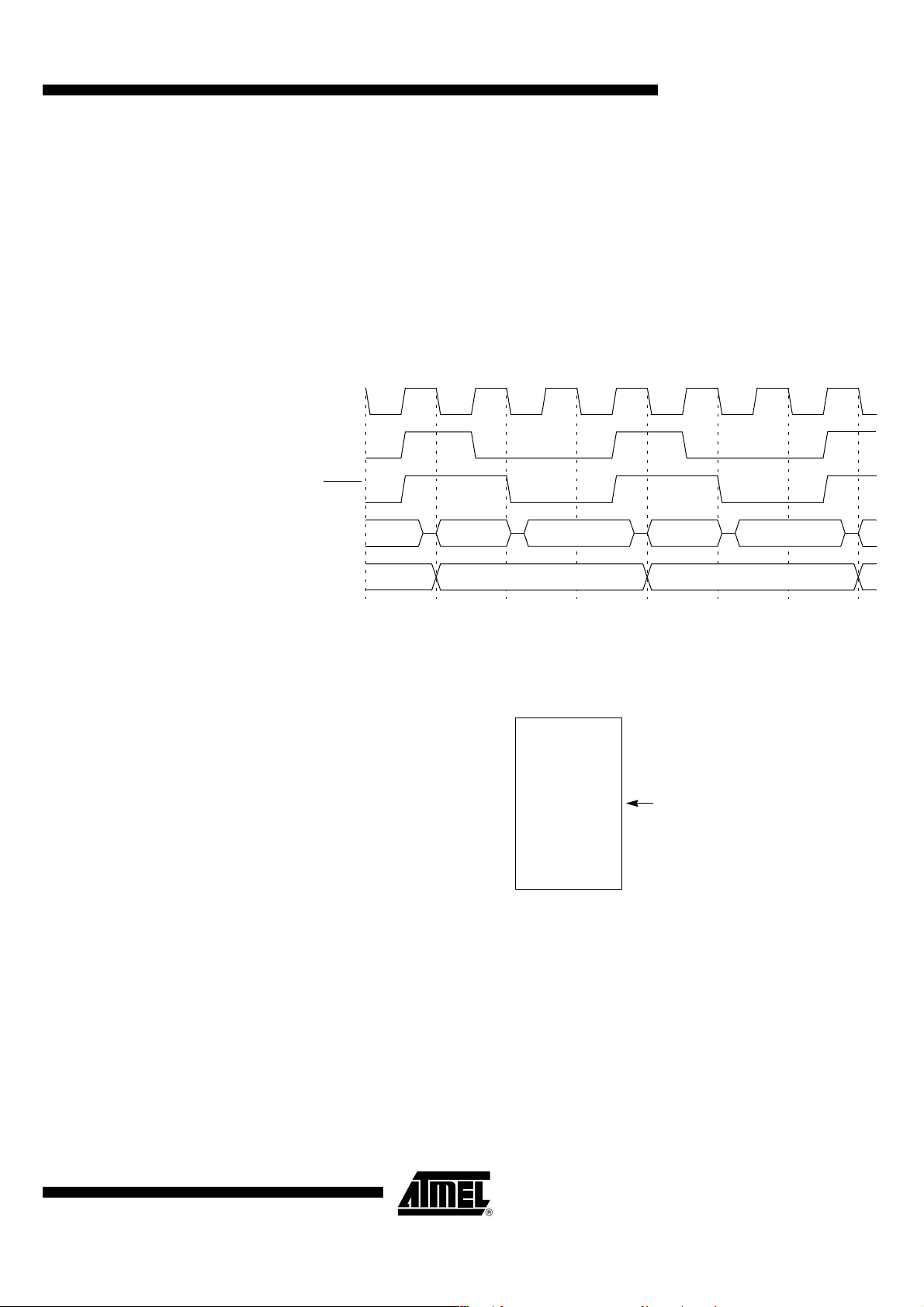
and KIN3:0) are sampled once per peripheral cycle (6
peripheral clock periods) (see Figure 25). A le ve l- tr ig gered interrupt pin held low or hig h
for more than 6 peripheral clock periods (12 oscillator in standard mode or 6 oscillator
clock periods in X2 mode) guar antees detectio n. Edge-trigger ed external i nterrupts
must hold the request pin low for at least 6 peripheral clock periods.
Figure 25. Minimum Pulse Timings
Level-Triggered Interrupt
> 1 Peripheral Cycle
1 cycle
4109H–8051–01/05
Edge-Triggered Interrupt
> 1 Peripheral Cycle
1 cycle 1 cycle
41

AT8xC51SND1C
10.6 Registers Table 7. IEN0 Regi st er
IEN0 (S:A8h) – Interrupt Enable Register 0
76543210
EA EAUD EMP3 ES ET1 EX1 ET0 EX0
Bit
Number
7EA
6 EAUD
5EMP3
4ES
3ET1
2EX1
1ET0
Bit
Mnemonic Description
Enable All Interrupt Bit
Set to enable all interrupts.
Clear to disable all interrupts.
If EA = 1, each interrupt source is individually enabled or disabled by setting or
clearing its interrupt enable bit.
Audio Interface Interrupt Enable Bit
Set to enable audio interface interrupt.
Clear to disable audio interface interrupt.
MP3 Decoder Interrupt Enable Bit
Set to enable MP3 decoder interrupt.
Clear to disable MP3 decoder interrupt.
Serial Port Interrupt Enable Bit
Set to enable serial port interrupt.
Clear to disable serial port interrupt.
Timer 1 Overflow Interrupt Enable Bit
Set to enable timer 1 overflow interrupt.
Clear to disable timer 1 overflow interrupt.
External Interrupt 1 Enable bit
Set to enable external interrupt 1.
Clear to disable external interrupt 1.
Timer 0 Overflow Interrupt Enable Bit
Set to enable timer 0 overflow interrupt.
Clear to disable timer 0 overflow interrupt.
42
0EX0
External Interrupt 0 Enable Bit
Set to enable external interrupt 0.
Clear to disable external interrupt 0.
Reset Value = 0000 0000b
4109H–8051–01/05

AT8xC51SND1C
Table 8. IEN1 Regi st er
IEN1 (S:B1h) – Interrupt Enable Register 1
76543210
- EUSB - EKB EADC ESPI EI2C EMMC
Bit
Number
7-
6EUSB
5-
4EKB
3 EADC
2ESPI
1EI2C
0EMMC
Bit
Mnemonic Description
Reserved
The value read from this bit is always 0. Do not set this bit.
USB Interface Interrupt Enable Bit
Set this bit to enable USB interrupts.
Clear this bit to disable USB interrupts.
Reserved
The value read from this bit is always 0. Do not set this bit.
Keyboard Interface Interrupt Enable Bit
Set to enable Keyboard interrupt.
Clear to disable Keyboard interrupt.
A to D Converter Interrupt Enable Bit
Set to enable ADC interrupt.
Clear to disable ADC interrupt.
SPI Controller Interrupt Ena ble Bit
Set to enable SPI interrupt.
Clear to disable SPI interrupt.
Two Wire Controller Interrupt Enable Bit
Set to enable Two Wire interrupt.
Clear to disable Two Wire interrupt.
MMC Interface Interrupt Enable Bit
Set to enable MMC interrupt.
Clear to disable MMC interrupt.
4109H–8051–01/05
Reset Value = 0000 0000b
43

AT8xC51SND1C
Table 9. IPH0 Regi st er
IPH0 (S:B7h) – Interrupt Priority High Register 0
76543210
- IPHAUD IPHMP3 IPHS IPHT1 IPHX1 IPHT0 IPHX0
Bit
Number
7-
6IPHAUD
5IPHMP3
4IPHS
3IPHT1
2IPHX1
1IPHT0
0IPHX0
Bit
Mnemonic Description
Reserved
The value read from this bit is indeterminate. Do not set this bit.
Audio Interface Interrupt Priority Level MSB
Refer to Table 3 for priority level description.
MP3 Decoder Interrupt Priority Level MSB
Refer to Table 3 for priority level description.
Serial Port Interrupt Priority Level MSB
Refer to Table 3 for priority level description.
Timer 1 Interrupt Priority Level MSB
Refer to Table 3 for priority level description.
External Interrupt 1 Priority Level MSB
Refer to Table 3 for priority level description.
Timer 0 Interrupt Priority Level MSB
Refer to Table 3 for priority level description.
External Interrupt 0 Priority Level MSB
Refer to Table 3 for priority level description.
Reset Value = X000 0000b
44
4109H–8051–01/05

AT8xC51SND1C
Table 10. IPH1 Register
IPH1 (S:B3h) – Interrupt Priority High Register 1
76543210
- IPHUSB - IPHKB IPHADC IPHSPI IPHI2C IPHMMC
Bit
Number
7-
6 IPHUSB
5-
4IPHKB
3IPHADC
2IPHSPI
1IPHI2C
0IPHMMC
Bit
Mnemonic Description
Reserved
The value read from this bit is always 0. Do not set this bit.
USB Interrupt Priority Level MSB
Refer to Table 3 for priority level description.
Reserved
The value read from this bit is always 0. Do not set this bit.
Keyboard Interrupt Priority Level MSB
Refer to Table 3 for priority level description.
A to D Converter Interrupt Priority Level MSB
Refer to Table 3 for priority level description.
SPI Interrupt Priority Level MSB
Refer to Table 3 for priority level description.
Two Wire Controller Interrupt Priority Level MSB
Refer to Table 3 for priority level description.
MMC Interrupt Priority Level MSB
Refer to Table 3 for priority level description.
Reset Value = 0000 0000b
4109H–8051–01/05
45

AT8xC51SND1C
Table 11. IPL0 Register
IPL0 (S:B8h) - Interrupt Priority Low Register 0
76543210
- IPLAUD IPLMP3 IPLS IPLT1 IPLX1 IPLT0 IPLX0
Bit
Number
7-
6IPLAUD
5IPLMP3
4IPLS
3IPLT1
2IPLX1
1IPLT0
0IPLX0
Bit
Mnemonic Description
Reserved
The value read from this bit is indeterminate. Do not set this bit.
Audio Interface Interrupt Priority Level LSB
Refer to Table 3 for priority level description.
MP3 Decoder Interrupt Priority Level LSB
Refer to Table 3 for priority level description.
Serial Port Interrupt Priority Level LSB
Refer to Table 3 for priority level description.
Timer 1 Interrupt Priority Level LSB
Refer to Table 3 for priority level description.
External Interrupt 1 Priority Level LSB
Refer to Table 3 for priority level description.
Timer 0 Interrupt Priority Level LSB
Refer to Table 3 for priority level description.
External Interrupt 0 Priority Level LSB
Refer to Table 3 for priority level description.
Reset Value = X000 0000b
46
4109H–8051–01/05

AT8xC51SND1C
Table 12. IPL1 Register
IPL1 (S:B2h) – Interrupt Priority Low Register 1
76543210
- IPLUSB - IPLKB IPLADC IPLSPI IPLI2C IPLMMC
Bit
Number
7-
6IPLUSB
5-
4IPLKB
3IPLADC
2IPLSPI
1IPLI2C
0IPLMMC
Bit
Mnemonic Description
Reserved
The value read from this bit is always 0. Do not set this bit.
USB Interrupt Priority Level LSB
Refer to Table 3 for priority level description.
Reserved
The value read from this bit is always 0. Do not set this bit.
Keyboard Interrupt Priority Level LSB
Refer to Table 3 for priority level description.
A to D Converter Interrupt Priority Level LSB
Refer to Table 3 for priority level description.
SPI Interrupt Priority Level LSB
Refer to Table 3 for priority level description.
Two Wire Controller Interrupt Priority Level LSB
Refer to Table 3 for priority level description.
MMC Interrupt Priority Level LSB
Refer to Table 3 for priority level description.
Reset Value = 0000 0000b
4109H–8051–01/05
47
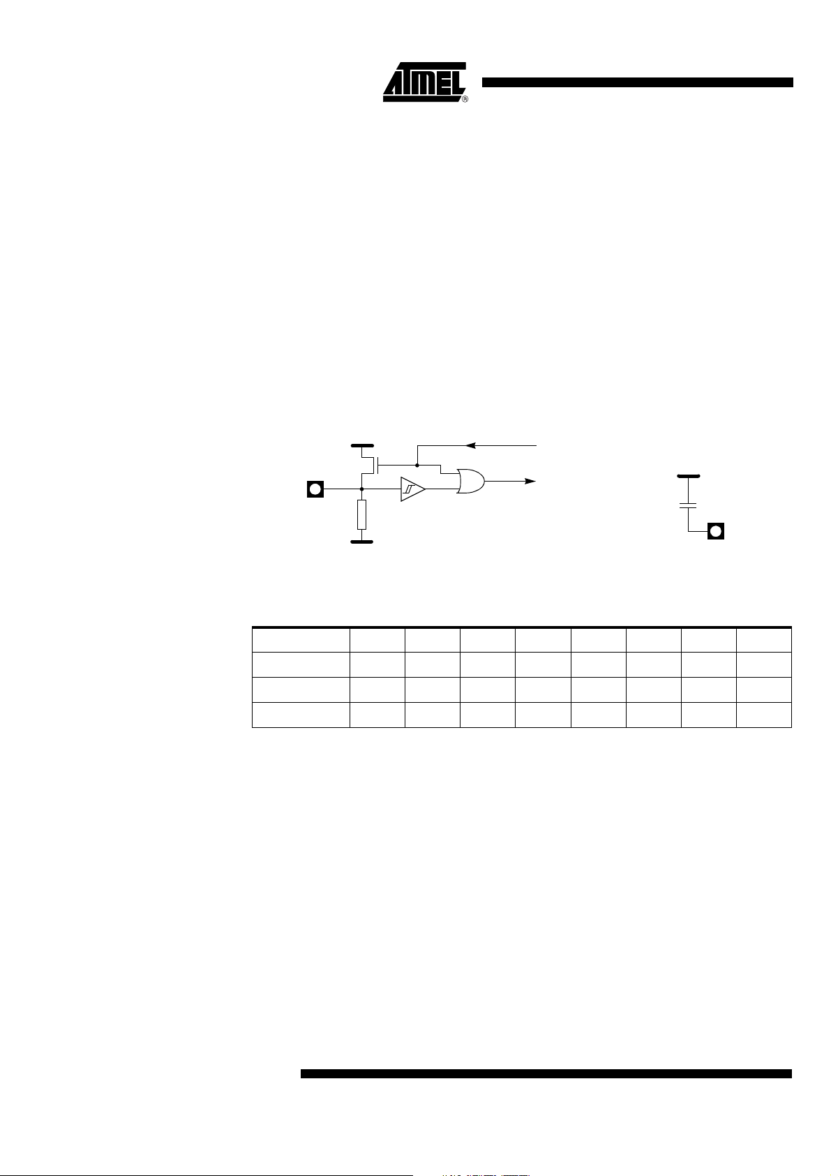
AT8xC51SND1C
11. Power
Management
2 power reduction modes are implemented in the AT8xC51SND1C: the Idle mode and
the Power-do wn mode . These modes ar e detai led in th e follo wing se ction s. In ad dition
to these power redu cti on mo des , t he cl oc ks o f th e c ore and peripherals can be dy nam ically divided by 2 using the X2 mode detailed in section “X2 Feature”, page 12.
11.1 Reset In order to start-up (cold reset) or to restart (warm reset) properly the microcontroller, an
high level has to be applied on the RST pin. A bad level leads to a wrong initialization of
the internal registers like SF Rs, Program Cou nter… and to unpredic table behavior of
the microcontroller. A proper device reset in itializes the AT8xC51SND1C and vector s
the CPU to address 0000h. RS T input has a pu ll-d own resi stor allo wing pow er-on r eset
by simply connecti ng an ex tern al cap acito r to V
can be applied eith er directl y on the RST pin or indirect ly by an inter nal reset so urce
such as the watchdog timer. Resistor value and input c haracteristics are dis cussed in
the Section “DC Characteristics” of the AT8xC51SND1C datasheet. The status of the
Port pins during reset is detailed in Table 2.
Figure 26. Reset Circuitry and Power-On Reset
VDD
P
RST
RST
R
VSS
as shown in Figure 26. A wa rm res et
DD
From Internal
Reset Source
To CPU Core
and Peripherals
VDD
+
RST
Table 2. Pin Conditions in Special Operating Modes
Mode Port 0 Port 1 Port 2 Port 3 Port 4 Port 5 MMC Audio
Reset Floating High High High High High Floating
Idle Data Data Data Data Data Data Data Data
Power-down Data Data Data Data Data Data Data Data
Note: 1. Refer to section “Audio Output Interface”, page 75.
11.2.1 Cold Reset 2 conditions are required before enabling a CPU start-up:
•V
must reach the specified VDD range
DD
• The level on X1 input pin must be outside the specification (V
If one of these 2 conditions are not me t, the mic rocontr oll er does no t start correc tly and
can execute an instruction fetch from anywhere in the program s pace. An active leve l
applied on the RST pin must be maintained till both of the above conditions are met. A
reset is active when the level V
period of time wher e V
and the oscillator are not stabilized. 2 parameters have to be
DD
is reached and wh en the pulse width covers the
IH1
taken into account to determine the reset pulse width:
•V
rise time,
DD
• Oscillator startup time.
Power-on ResetRST input circuitry
IH
1
, VIL)
48
To determine the capacitor value to implement, the highest value of these 2 parameters
has to be chosen. Table 3 gives some capacitor values examples for a minimum R
50 KΩ and different oscillator startup and V
rise times.
DD
4109H–8051–01/05
RST
of
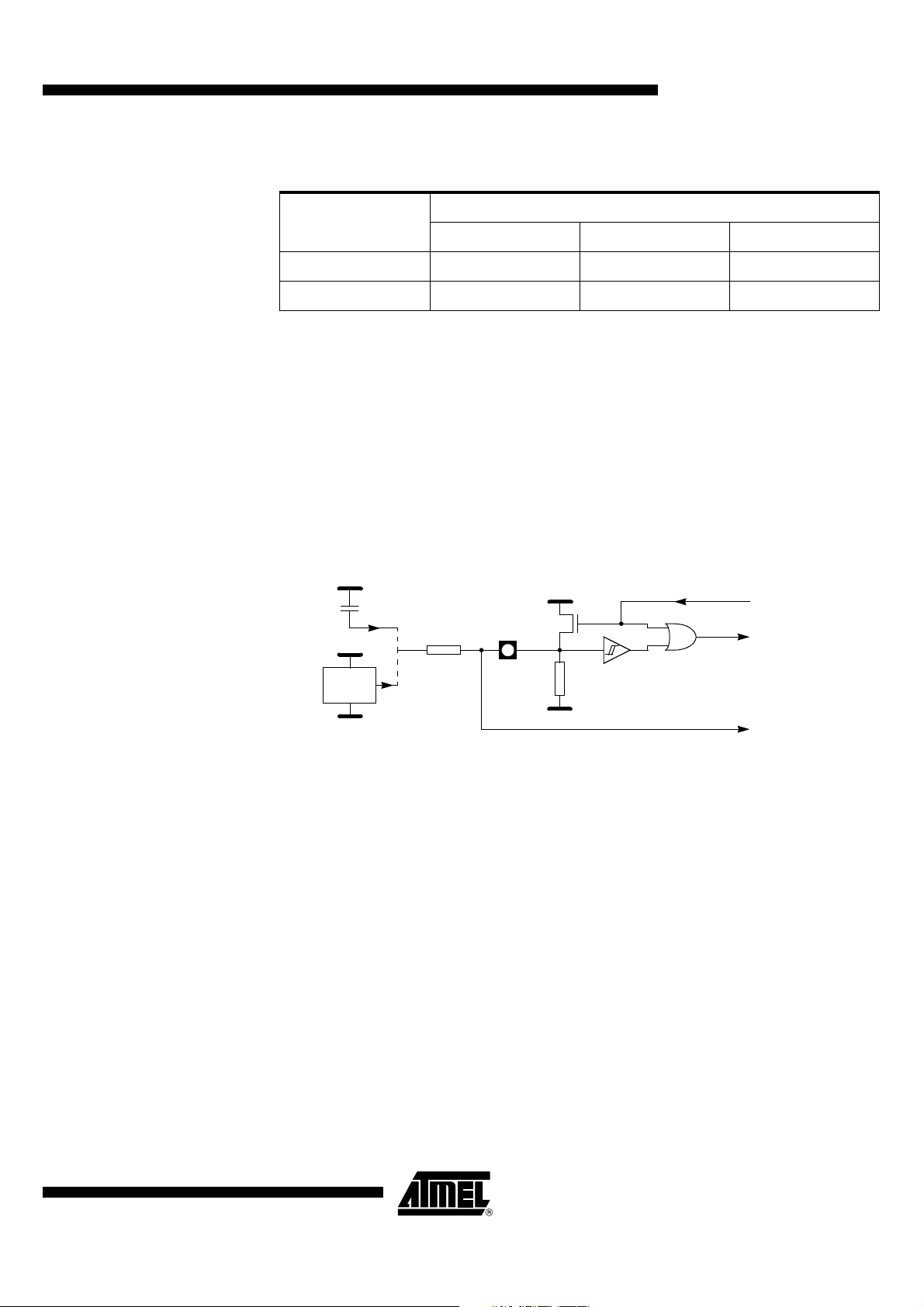
AT8xC51SND1C
Table 3. Minimum Reset Capacitor Value for a 50 kΩ Pull-down Resistor
Oscillator
Start-Up Time
5 ms 820 nF 1.2 µF 12 µF
20 ms 2.7 µF 3.9 µF 12 µF
Note: 1. These values assume VDD starts from 0V to the nominal value. If the time between 2
on/off sequences is too fast, the power-supply de-coupling capacitors may not be
fully discharged, leading to a bad reset sequence.
1 ms 10 ms 100 ms
VDD Rise Time
(1)
11.3.1 Warm Reset To achieve a valid reset, the reset signal must be maintained for at least 2 machine
cycles (24 oscillator clock periods) while the oscillator is running. The number of clock
periods is mode independent (X2 or X1).
11.3.2 Watchdog Reset As detailed in section “Watchdog Timer”, page 61, the WDT generates a 96-clock period
pulse on the RST pin. In order to properly propagate this pulse to the rest of the application in case of external capacitor or power-supply supervisor circuit, a 1 kΩ resistor must
be added as shown in Figure 27.
Figure 27. Reset Circuitry for WDT Reset-out Usage
VDD
VDD
+
RST
1K
VDD
From WDT
P
Reset Source
To CPU Core
and Peripherals
RST
VSS
R
To Other
On-board
Circuitry
11.4 Reset
Recommendation to
Prevent Flash Corruption
RST
VSS
An example of bad initialization situation may occur in an instance where the bit
ENBOOT in AUXR1 registe r is initiali zed from the har dware bit BLJB upon reset. Sinc e
this bit allows mapping of the bootloader in the code area, a reset failure can be critical.
If one wants the ENBOOT cleared in order to unmap the boot from the code area (yet
due to a bad reset) the b it ENBOOT in SFRs may be set. If the value of Progra m
Counter is accidently in the range of the boot memory addresses then a Flash access
(write or erase) may corrupt the Flash on-chip memory.
It is recommended to use an external reset circuitry featuring power supply monitoring to
prevent system malfunction during periods of insufficient power supply voltage (power
supply failure, power supply switched off).
11.5 Idle Mode Idle mode is a power reduction mode that reduces the power consumption. In this mode,
program execution halts. Idle mode freezes the cl ock to the CPU at known sta tes while
the peripherals continue to be clocked (refer to section “Oscillator”, page12). The CPU
status before entering Idle mode is preserve d, i.e., the program cou nter and p rogram
status word register retain their data for the duration of Idle mode. The contents of the
SFRs and RAM are also retai ned. The status of the Po rt pins during Idle mod e is
detailed in Table 2.
4109H–8051–01/05
49

AT8xC51SND1C
11.5.1 Entering Idle Mode To enter Idle mode, the user must set the IDL bit in PCON register (see Table 8). The
AT8xC51SND1C enters Idle mode upon e xecution of t he instructi on that sets I DL bit.
The instruction that sets IDL bit is the last instruction executed.
Note: If IDL bit and PD bit are set simultaneously, the AT8xC51SND1C enter Power-down
mode. Then it does not go in Idle mode when exiting Power-down mode.
11.5.2 Exiting Idle Mode There are 2 ways to exit Idle mode:
1. Generate an enabled interrupt.
– Hardware clears IDL bit in PCON register which restores the clock to the
CPU. Execution resumes with the interrupt service routine. Upon completion
of the interrupt service routine, program execution resumes with the
instruction immediately following the instruction that activated Idle mode.
The general-purpose flags (GF1 and GF0 in PCON register) may be used to
indicate whether an interrupt occurred during normal operation or during Idle
mode. When Idle mode is exited by an interrupt, the interrupt service routine
may examine GF1 and GF0.
2. Generate a reset.
– A logic high on the RST pin clears IDL bit in PCON register directly and
asynchronously. This restores the clock to the CPU. Program execution
momentarily resumes with the instruction immediately following the
instruction that activated the Idle mode and may continue for a number of
clock cycles before the internal reset algorithm takes control. Reset
initializes the AT8xC51SND1C and vectors the CPU to address C:0000h.
Note: During the time that execution resumes, the in tern al R AM cann ot be acces se d; however,
it is possible for the Port pins to be accessed. To avoid unexpected outputs at the Port
pins, the instruction immediately following the instruction that activated Idle mode should
not write to a Port pin or to the external RAM.
11.6 Power-down Mode The Power-down mode places the AT8xC51SND1C in a very low power state. Power-
down mode stops the os c illat or and free zes all c lock s a t kn own s tat es (ref er to the Se ction "Oscillator", page 12). The CPU status prior to ente ring Power-down mode is
preserved, i.e., the program counter, program status word register retain their data for
the duration of Power-down mode. In addition, the SFRs and RAM contents are preserved. The status of the Port pins during Power-down mode is detailed in Table 2.
11.6.1 Entering Power-down
Mode
11.6.2 Exiting Power-down
Mode
Note: VDD may be reduced to as l ow as V
dissipation. Notice, however, that V
To enter Power-down mode, set PD bit in PCON register. The AT8xC51SND1C enters
the Power-down mode upon execution of the instruction that sets PD bit. The instruction
that sets PD bit is the last instruction executed.
If V
was reduced during the Power-down mode, do not exit Power-down mode until
DD
V
is restored to the normal operating level.
DD
There are 2 ways to exit the Power-down mode:
1. Generate an enabled external interrupt.
– The AT8xC51SND1C provides capability to exit from Power-down using
INT0
, INT1, and KIN3:0 inputs. In addition, using KIN input provides high or
low level exit capability (see section “Keyboard Interface”, page 182).
Hardware clears PD bit in PCON register which starts the oscillator and
restores the clocks to the CPU and peripherals. Using INTn
during Power-down mode to further reduce power
RET
is not reduced until Power-down mode is invoked.
DD
input, execution
50
4109H–8051–01/05
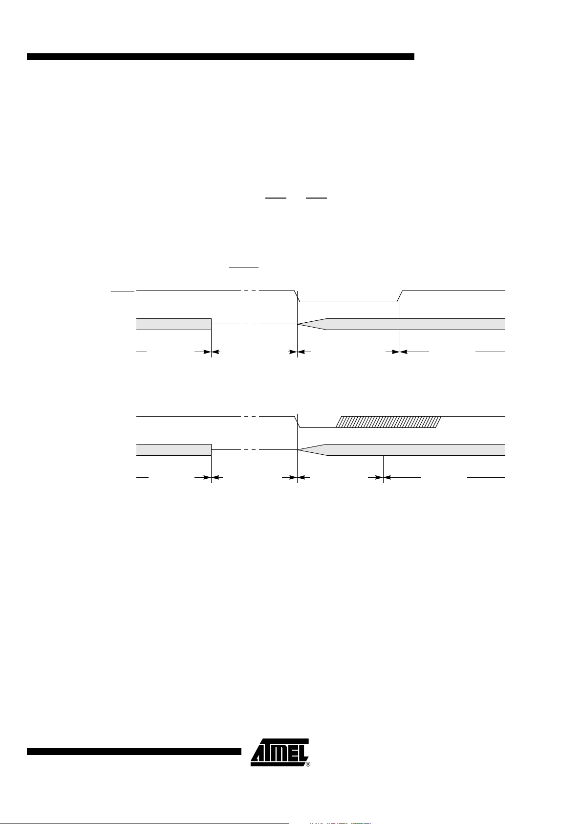
resumes when the input is released (see Figure 28) while using KINx input,
execution resumes after counting 1024 clock ensuring the oscillator is
restarted properly (see Figure 29). This behavior is necessary for decoding
the key while it is still pressed. In both cases, execution resumes with the
interrupt service routine. Upon completion of the interrupt service routine,
program execution resumes with the instruction immediately following the
instruction that activated Power-down mode.
Note: 1. The external interrupt used to exit Power-down mode must be configured as level
sensitive (
duration of the interrupt must be long enough to allow the oscillator to stabilize. The
execution will only resume when the interrupt is deasserted.
2. Exit from power-down by external interrupt does not affect the SFRs nor the internal
RAM content.
Figure 28. Power-down Exit Waveform Using INT1:0
INT1:0
OSC
AT8xC51SND1C
INT0 and INT1) and must be assigned the highest priority. In addition, the
Power-down Phase
Figure 29. Power-down Exit Waveform Using KIN3:0
1
KIN3:0
OSC
Power-down Phase
Note: 1. KIN3:0 can be high or low-level triggered.
2. Generate a reset.
– A logic high on the RST pin clears PD bit in PCON register directly and
asynchronously. This starts the oscillator and restores the clock to the CPU
and peripherals. Program execution momentarily resumes with the
instruction immediately following the instruction that activated Power-down
mode and may continue for a number of clock cycles before the internal
reset algorithm takes control. Reset initializes the AT8xC51SND1C and
vectors the CPU to address 0000h.
Notes: 1. Du r ing t he tim e t h at ex e cu ti o n re su mes, t h e int e rna l RA M ca n not be ac ce ss ed; ho w-
ever, it is possible for the Port pins to be accessed. To avoid unexpected outputs at
the Port pins, the instruction immediately following the instruction that activated the
Power-down mode should not write to a Port pin or to the external RAM.
2. Exit from power-down by res et r ede fine s a ll the SFRs, but does not af f ec t the internal
RAM content.
Oscillator Restart Phase
1024 clock count Active phaseActive phase
Active PhaseActive phase
4109H–8051–01/05
51

AT8xC51SND1C
11.7 Registers Table 8. PCON Register
PCON (S:87h) – Power Configuration Register
76543210
SMOD1 SMOD0 - - GF1 GF0 PD IDL
Bit
Number
7SMOD1
6SMOD0
5 - 4 -
3GF1
2GF0
1PD
0IDL
Bit
Mnemonic Description
Serial Port Mo de Bit 1
Set to select double baud rate in mode 1,2 or 3.
Serial Port Mo de Bit 0
Set to select FE bit in SCON register.
Clear to select SM0 bit in SCON register.
Reserved
The value read from these bits is indeterminate. Do not set these bits.
General-Purpose Flag 1
One use is to indicate whether an interrupt occurred during normal operation or
during Idle mode.
General-Purpose Flag 0
One use is to indicate whether an interrupt occurred during normal operation or
during Idle mode.
Power-Down Mode Bit
Cleared by hardware when an interrupt or reset occurs.
Set to activate the Power-down mode.
If IDL and PD are both set, PD takes precedence.
Idle Mode Bit
Cleared by hardware when an interrupt or reset occurs.
Set to activate the Idle mode.
If IDL and PD are both set, PD takes precedence.
Reset Value = 00XX 0000b
52
4109H–8051–01/05

AT8xC51SND1C
12. Timers/ Counters The AT8xC51SND1C implement 2 general-purpose, 16-bit Timers/Counters. They are
identified as Timer 0 and Timer 1, an d can be in depende ntly confi gured to operate in a
variety of modes as a Timer or as an event Coun ter. When op erating a s a Timer, th e
Timer/Counter runs for a programmed length of time, then issues an interrupt request.
When operating as a Counter, the Tim er/Counter counts n egative transit ions on an
external pin. After a preset number of counts, the Counter issues an interrupt request.
The various o perating modes o f each Ti mer/Count er are de scribed in the fo llowing
sections.
12.1 Timer/Counter
Operations
For instance, a basic operation is Timer registers THx and TLx (x = 0, 1) connected in
cascade to form a 16-bit Timer. Setting the run control bit (TRx) in TCON register (see
Table 7) turns the Ti mer o n by allowi ng t he s elec ted input to i ncrem ent T Lx. Whe n TLx
overflows it increments THx; when THx overflows it sets the Timer overflow flag (TFx) in
TCON register. S ettin g the TRx doe s not clea r the THx an d TLx Tim er regis ters. T imer
registers can be ac cessed to obtain the curr ent count or to enter preset va lues. T hey
can be read at any time but TRx bit must be cleared to preset their values, otherwise,
the behavior of the Timer/Counter is unpredictable.
The C/Tx# control bit selects Timer operation or Counter operation by selecting the
divided-down peripheral clock or external pin T x as the source for the counted signal.
TRx bit must be cleared when changing the mode of operation, otherwise the behavior
of the Timer/Counter is unpredictable.
For Timer op erat ion (C/Tx # = 0 ), t he T ime r reg ist er co unts the divid ed-d own peri phera l
clock. The Timer register is incremented once every peripheral cycle (6 peripheral clock
periods). The Time r cloc k rat e is F
/6, i.e., F
PER
/12 in standard mo de or F
OSC
OSC
/6 in X2
mode.
For Counter operation (C/Tx # = 1), the T im er reg ister cou nts the neg ati ve tran si ti ons on
the Tx external input pin. The external input is sampled every peripheral cycles. When
the sample is high in one cycle and low in the next one, the Counter is incremented.
Since it takes 2 cycles (12 peripheral clock periods) to recognize a negative transition,
the maximum count rate is F
/12, i.e., F
PER
/24 in standard mode or F
OSC
/12 in X2
OSC
mode. There are no restrictions on the duty cycle of the external input signal, but to
ensure that a given level is sampled at least once before it changes, it should be held for
at least one full peripheral cycle.
12.2 Timer Clock
Controller
4109H–8051–01/05
As shown in Figure 30 , the Timer 0 (F T0) and Timer 1 (FT1) clock s are derive d from
either the peripheral clock (F
) or the oscillator clock (F
PER
) depending on the T0X2
OSC
and T1X2 bits i n CKCON r egister. These c locks a re issu ed from the Clo ck Contro ller
block as deta iled in Secti on “Cl ock Co ntro ller” , pa ge 12 . Wh en T0 X2 or T 1X2 bit is s et,
the Timer 0 or Timer 1 clock frequency is fix ed and equal to the oscillator cl ock frequency divided by 2. Whe n cleared, the Timer cloc k frequen cy is equal to the oscillat or
clock frequency divi ded by 2 in s tand ar d m ode or to the oscillator clock fr eq uenc y i n X 2
mode.
53
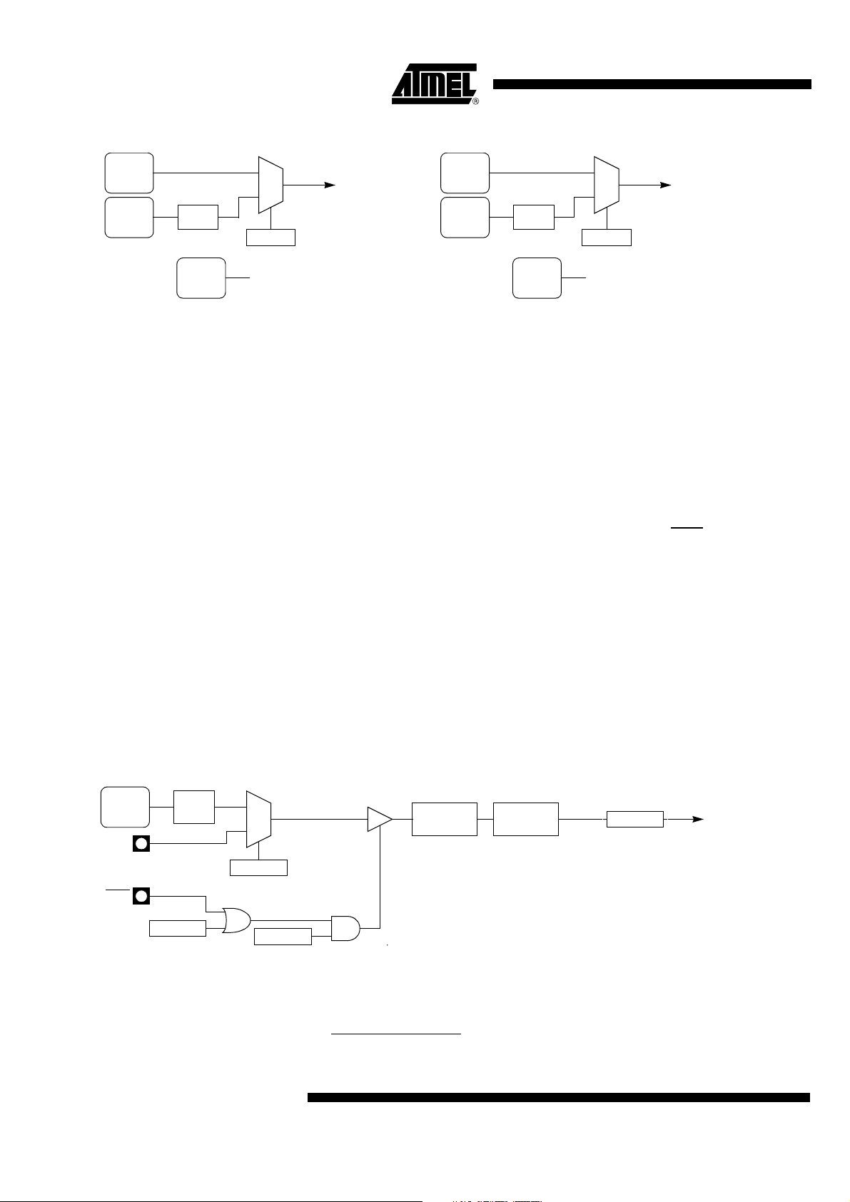
AT8xC51SND1C
Figure 30. Timer 0 and Timer 1 Clock Controller and Symbols
k
PER
CLOCK
OSC
CLOCK
÷ 2
TIM0
CLOCK
0
Timer 0 Clock
1
T0X2
CKCON.1
PER
CLOCK
OSC
CLOCK
0
Timer 1 Cloc
1
÷ 2
T1X2
CKCON.2
TIM1
CLOCK
Timer 0 Clock Symbol
Timer 1 Clock Symbol
12.3 Timer 0 Timer 0 functions as either a Timer or event Counter in four modes of operation.
Figure 31 through Figure 37 show the logical configuration of each mode.
Timer 0 is controlled by the four lo wer bits of TMO D regis te r (se e Tabl e 8) and bits 0, 1,
4 and 5 of TCON register (see Table 7). TMOD register selects the method of Timer gating (GATE0), Timer or Counter op eration (C/T0#) and mode of operation (M10 and
M00). TCON register provides Timer 0 control functions: overflow flag (TF0), run control
bit (TR0), interrupt flag (IE0) and interrupt type control bit (IT0).
For normal Timer ope ratio n (GAT E0 = 0) , se tting TR 0 allows TL 0 to be increme nted by
the selected input. Settin g GATE0 and TR0 allow s external pin IN T0
operation.
Timer 0 overflow (count rolls over from all 1s to all 0s) sets TF0 flag generating an interrupt request.
It is important to stop Timer/Counter before changing mode.
12.3.1 Mode 0 (13-bit Timer) Mode 0 configures Timer 0 as a 13-bit Timer which is set up as an 8-bit Timer (TH0 register) with a modulo 32 pre scaler implem ented with the lo wer five bits of TL0 r egister
(see Figure 31) . The upper three bits of TL0 register are indeterminate and s hould be
ignored. Prescaler overflow increments TH0 register. Figure 32 gives the overflow
period calculation form ula.
to control Timer
Figure 31. Timer/Counter x (x = 0 or 1) in Mode 0
TIMx
CLOCK
Tx
INTx
÷ 6
GATEx
TMOD Reg
0
1
C/Tx#
TMOD Reg
TRx
TCON Reg
Figure 32. Mode 0 Overflow Period Formula
TFx
6 ⋅ (16384 – (THx, TLx))
=
PER
54
F
TIMx
TLx
(5 Bits)
THx
(8 Bits)
Overflow
TFx
TCON reg
Timer x
Interrupt
Request
4109H–8051–01/05
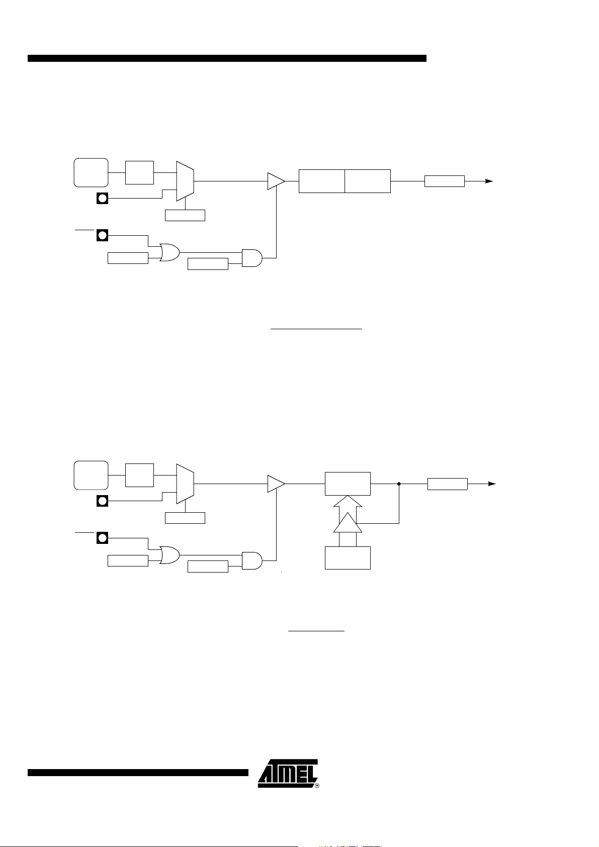
AT8xC51SND1C
t
t
t
t
12.3.2 Mode 1 (16-bit Timer) Mode 1 configures Timer 0 as a 16-bit Timer with TH0 and TL0 registers connected in
cascade (see Figure 33). The selected input increments TL0 register. Figure 34 gives
the overflow period calculation formula when in timer mode.
Figure 33. Timer/Counter x (x = 0 or 1) in Mode 1
TIMx
CLOCK
÷ 6
0
1
Tx
C/Tx#
TMOD Reg
INTx
GATEx
TMOD Reg
TRx
TCON Reg
Figure 34. Mode 1 Overflow Period Formula
TFx
12.3.3 Mode 2 (8-bit Timer with
Auto-Reload)
Mode 2 configures Timer 0 as an 8-b it Timer (TL0 register) tha t automatically reloads
from TH0 register (see Table 9). TL0 overflow sets TF0 flag in TCON register and
reloads TL0 with the contents of TH0, which is preset by software. When the interrupt
request is servic ed, ha rdware clears TF0. The reload leaves TH0 unch anged. The next
reload value may be changed at any time by writing it to TH0 register. Figure 36 gives
the autoreload period calculation formula when in timer mode.
Figure 35. Timer/Counter x (x = 0 or 1) in Mode 2
⋅ (65536 – (THx, TLx))
6
=
PER
THx
(8 bits)
F
TIMx
TLx
(8 bits)
Overflow
TFx
TCON Reg
Timer x
Interrup
Reques
TIMx
CLOCK
÷ 6
0
1
TLx
(8 bits)
Overflow
TFx
TCON reg
Timer x
Interrup
Reques
Tx
C/Tx#
TMOD reg
INTx
THx
GATEx
TMOD reg
TRx
TCON reg
(8 bits)
Figure 36. Mode 2 Autoreload Period Formula
PER
=
6 ⋅ (256 – THx)
F
TIMx
TFx
12.3.4 Mode 3 (2 8-bit Timers) Mode 3 configures Timer 0 such that registers TL0 and TH0 operate as separate 8-bit
Timers (see Figure 37). This mode is provided for applications requiring an additional 8bit Timer or Counter. TL0 uses the Timer 0 control bits C/T0# and GATE0 in TMOD register, and TR0 and TF0 in TCON register in the normal manner. TH0 is locked into a
Timer function (counting F
/6) and takes over use of the Timer 1 interrupt (TF1) and
TF1
run control (TR1) bits. Thus , operation of Tim er 1 is restricted when Timer 0 is in mod e
4109H–8051–01/05
55
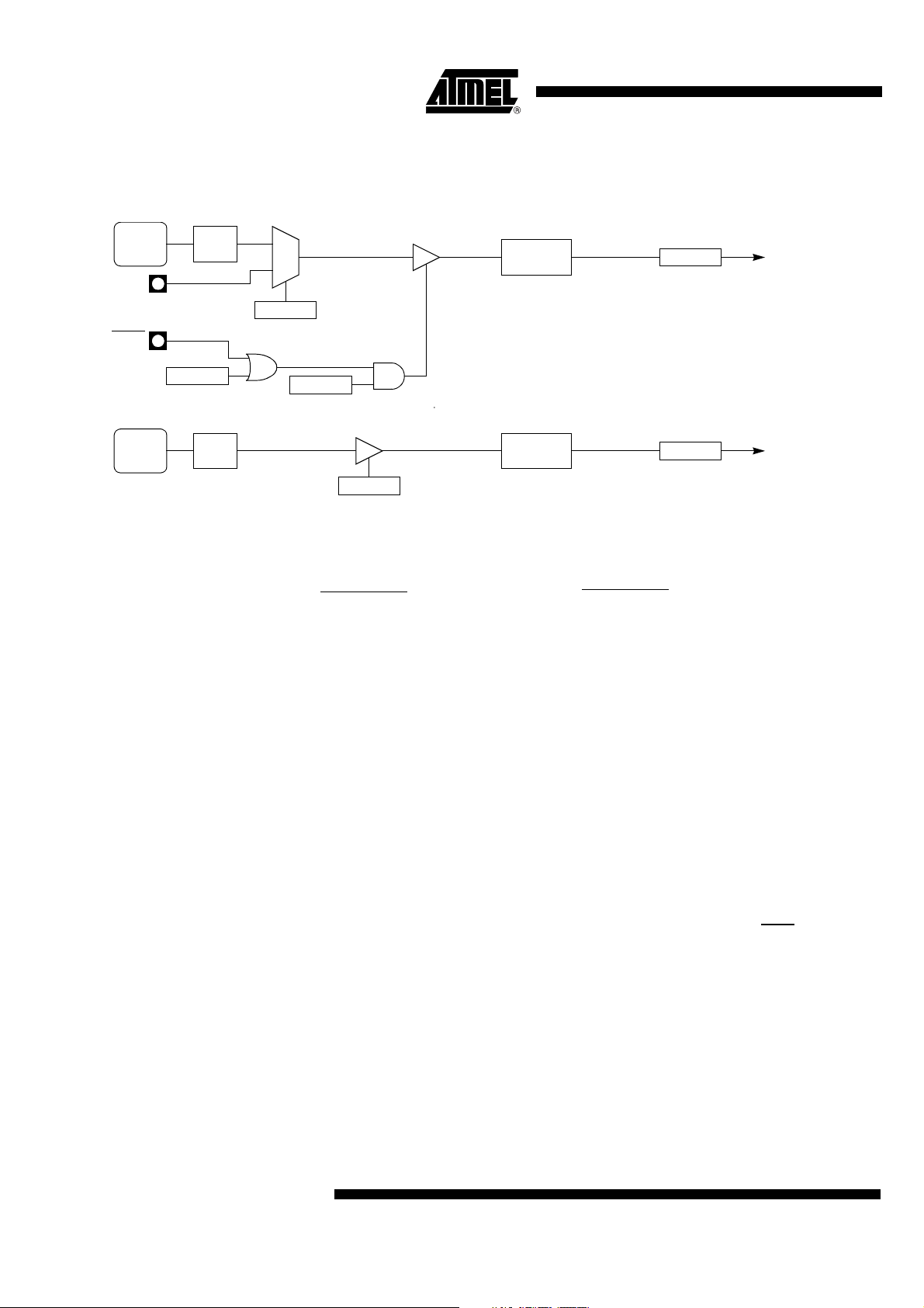
AT8xC51SND1C
3. Figure 36 gives the auto reload period c alculation formul as for both TF 0 and TF1
t
t
t
t
flags.
Figure 37. Timer/Counter 0 in Mode 3: 2 8-bit Counters
TIM0
CLOCK
T0
÷ 6
0
1
C/T0#
TMOD.2
INT0
TL0
(8 bits)
Overflow
TF0
TCON.5
Timer 0
Interrup
Reques
TIM0
CLOCK
GATE0
TMOD.3
÷ 6
TR0
TCON.4
TH0
(8 bits)
Overflow
TF1
TCON.7
Timer 1
Interrup
Reques
TR1
TCON.6
Figure 38. Mode 3 Overflow Period Formula
TF0
PER
=
6 ⋅ (256 – TL0)
F
TIM0
TF1
PER
=
6 ⋅ (256 – TH0)
F
TIM0
12.4 Timer 1 Timer 1 is identical to Timer 0 except for Mode 3 which is a hold-count mode. The fol-
lowing comments help to understand the differences:
• Timer 1 functio ns as either a Timer or event Cou nter in three modes of operation.
Figure 31 through Figure 35 show the logical configuration for modes 0, 1, and 2.
Timer 1’s mode 3 is a hold-count mode.
• Timer 1 is controlled by the four high-order bits of TMOD register (see Figure 8) and
bits 2, 3, 6 and 7 of TCON register (see Figure 7). TMOD register selects the
method of Timer gating (GATE1), Timer or Counter operation (C/T1#) and mode of
operation (M11 and M01). TCON register provides Timer 1 control functions:
overflow flag (TF1), run control bit (TR1), interrupt flag (IE1) and interrupt type
control bit (IT1).
• Timer 1 can serve as the Baud Rate Generator for the Serial Port. Mode 2 is best
suited for this purpose.
• For normal Timer operation (GATE1 = 0), setting TR1 allows TL1 to be incremented
by the selected input. Setting GATE1 and TR1 allows external pin INT1
Timer operation.
• Timer 1 overflow (count rolls over from all 1s to all 0s) sets the TF1 flag generating
an interrupt request.
• When Timer 0 is in mode 3, it uses Timer 1’s overflow flag (TF1) and run control bit
(TR1). For this situation, use Timer 1 only for applications that do not require an
interrupt (such as a Baud Rate Generator for the Serial Port) and switch Timer 1 in
and out of mode 3 to turn it off and on.
• It is important to stop the Timer/Counter before changing modes.
to control
56
4109H–8051–01/05
AT8xC51SND1C
12.4.1 Mode 0 (13-bit Timer) Mode 0 configures Timer 1 as a 13-bit Timer, which is set up as an 8-bit Timer (TH1 reg-
ister) with a modulo-32 prescaler implemented with the lower 5 bits of the TL1 register
(see Figure 31). The uppe r 3 bits of TL1 regi ster ar e ignor ed. Pre scaler overflo w incr ements TH1 register.
12.4.2 Mode 1 (16-bit Timer) Mode 1 configures Timer 1 as a 16-bit Timer with TH1 and TL1 registers connected in
cascade (see Figure 33). The selected input increments TL1 register.
12.4.3 Mode 2 (8-bit Timer with
Auto-Reload)
Mode 2 configures Timer 1 as an 8-bit Timer (TL1 register) with automatic reload from
TH1 register on ove rflow ( see Figu re 35) . TL1 ov erflow s ets TF 1 flag i n TCON r egiste r
and reloads TL1 with the contents of TH1, which is preset by software. The reload
leaves TH1 unchanged.
12.4.4 Mode 3 (Halt) Plac ing Timer 1 in mode 3 causes it to halt and ho ld its coun t. This can be use d to halt
Timer 1 when TR1 run control bit is not available i.e. when Timer 0 is in mode 3.
12.5 Interrupt Each Timer handles one interrupt source that is the timer overflow flag TF0 or TF1. This
flag is set every time an overfl ow oc c urs. Fla gs are cl eared when v ec toring to the Timer
interrupt routine. Interrupts are enabled by setting ETx bit in IEN0 register. This
assumes interrupts are globally enabled by setting EA bit in IEN0 register.
Figure 39. Timer Interrupt System
TF0
TCON.5
ET0
IEN0.1
TF1
TCON.7
ET1
IEN0.3
Timer 0
Interrupt Request
Timer 1
Interrupt Request
4109H–8051–01/05
57

AT8xC51SND1C
12.6 Registers Table 7. TCON Register
TCON (S:88h) – Timer/Counter Control Register
76543210
TF1 TR1 TF0 TR0 IE1 IT1 IE0 IT0
Bit
Number
7TF1
6TR1
5TF0
4TR0
3IE1
2IT1
1IE0
Bit
Mnemonic Description
Timer 1 Overflow Flag
Cleared by hardware when processor vectors to interrupt routine.
Set by hardware on Timer/Counter overflow, when Timer 1 register overflows.
Timer 1 Run Control Bit
Clear to turn off Timer/Counter 1.
Set to turn on Timer/Counter 1.
Timer 0 Overflow Flag
Cleared by hardware when processor vectors to interrupt routine.
Set by hardware on Timer/Counter overflow, when Timer 0 register overflows.
Timer 0 Run Control Bit
Clear to turn off Timer/Counter 0.
Set to turn on Timer/Counter 0.
Interrupt 1 Edge Flag
Cleared by hardware when interrupt is processed if edge-triggered (see IT1).
Set by hardware when external interrupt is detected on INT1
Interrupt 1 Type Control Bit
Clear to select low level active (level triggered) for external interrupt 1 (INT1
Set to select falling edge active (edge triggered) for external interrupt 1.
Interrupt 0 Edge Flag
Cleared by hardware when interrupt is processed if edge-triggered (see IT0).
Set by hardware when external interrupt is detected on
pin.
INT0 pin.
).
0IT0
Interrupt 0 Type Control Bit
Clear to select low level active (level triggered) for external interrupt 0 (INT0
Set to select falling edge active (edge triggered) for external interrupt 0.
Reset Value = 0000 0000b
).
58
4109H–8051–01/05

AT8xC51SND1C
Table 8. TMO D Regi st er
TMOD (S:89h) – Timer/Counter Mode Control Register
76543210
GATE1 C/T1# M11 M01 GATE0 C/T0# M10 M00
Bit
Number
7GATE1
6C/T1#
5M11Timer 1 Mode Select Bits
4M01
3GATE0
2C/T0#
1
0
Bit
Mnemonic Description
Timer 1 Gating Control Bit
Clear to enable Timer 1 whenever TR1 bit is set.
Set to enable Timer 1 only while INT1
Timer 1 Counter/Timer Select Bit
Clear for Timer operation: Timer 1 counts the divided-down system clock.
Set for Counter operation: Timer 1 counts negative transitions on external pin T1.
M01 Operating mode
M11
0 0 Mode 0: 8-bit Timer/Counter (TH1) with 5-bit prescaler (TL1).
0 1 Mode 1: 16-bit Timer/Counter.
1 0 Mode 2: 8-bit auto-reload Timer/Counter (TL1).
1 1 Mode 3: Timer 1 halted. Retains count.
Timer 0 Gating Control Bit
Clear to enable Timer 0 whenever TR0 bit is set.
Set to enable Timer/Counter 0 only while
Timer 0 Counter/Timer Select Bit
Clear for Timer operation: Timer 0 counts the divided-down system clock.
Set for Counter operation: Timer 0 counts negative transitions on external pin T0.
M10 Timer 0 Mode Select Bit
M00
M10
M00 Operating mode
0 0 Mode 0: 8-bit Timer/Counter (TH0) with 5-bit prescaler (TL0).
0 1 Mode 1: 16-bit Timer/Counter.
1 0 Mode 2: 8-bit auto-reload Timer/Counter (TL0).
1 1 Mode 3: TL0 is an 8-bit Timer/Counter.
TH0 is an 8-bit Timer using Timer 1’s TR0 and TF0 bits.
Notes: 1. Reloaded from TH1 at overflo w.
2. Reloaded from TH0 at overflow.
pin is high and TR1 bit is set.
(1)
INT0 pin is high and TR0 bit is set.
(2)
4109H–8051–01/05
Reset Value = 0000 0000b
Table 9. TH0 Register
TH0 (S:8Ch) – Timer 0 High Byte Register
76543210
--------
Bit
Number
7:0 High Byte of Timer 0
Bit
Mnemonic Description
Reset Value = 0000 0000b
59

AT8xC51SND1C
Table 10. TL0 Register
TL0 (S:8Ah) – Timer 0 Low Byte Register
76543210
--------
Bit
Number
7:0 Low Byte of Timer 0
Bit
Mnemonic Description
Reset Value = 0000 0000b
Table 11. TH1 Register
TH1 (S:8Dh) – Timer 1 High Byte Register
76543210
--------
Bit
Number
7:0 High Byte of Timer 1
Bit
Mnemonic Description
Reset Value = 0000 0000b
Table 12. TL1 Register
TL1 (S:8Bh) – Timer 1 Low Byte Register
76543210
--------
Bit
Number
7:0 Low Byte of Timer 1
Bit
Mnemonic Description
Reset Value = 0000 0000b
60
4109H–8051–01/05

AT8xC51SND1C
l
13. Watchdog Timer The AT8xC51SND1C im pl eme nt a hardwa re Wa tc hdo g Tim er ( WDT) tha t au toma tical ly
resets the chip if it is allowed to time out. The WDT provides a means of recovering from
routines that do not complete successfully due to software or hardware malfunctions.
13.1 Description The WDT consists of a 14-bit prescaler followed by a 7-bit programmable counter. As
shown in Figure 40, the 14-bit prescaler is fed by the WDT clock detailed in
Section “Watchdog Clock Controller”, page 61.
The Watchdog Timer Reset regi ste r (WDTRS T , see Tab le 6) provi des con tr ol ac ce ss to
the WDT, while the Watchdog Timer Program register (WDTPRG, see Figure 43) provides time-out period programming.
Three operations contr ol the WDT:
• Chip reset clears and disables the WDT.
• Programming the time-out value to the WDTPRG register.
• Writing a specific 2-Byte sequence to the WDTRST register clears and enables the
WDT.
Figure 40. WDT Block Diagram
WDT
CLOCK
System Reset
13.2 Watchdog Clock
Controller
÷ 6
1Eh-E1h Decoder
RST
WDTRST
As shown in Figure 41 th e WD T clock (F
(F
) or the oscillator clock (F
PER
These clocks are issued from the Clock Controller block as detailed in S ection "Clock
Controller", page 12. When WTX2 bit is set, the WDT clock frequency is fixed and equal
to the oscillator clock frequency divided by 2. When cleared, the WDT clock frequency is
equal to the os cill ator cl oc k fr eq uen cy d iv id ed by 2 in standard m ode o r to th e o sc i lla tor
clock frequency in X2 mode.
Figure 41. WDT Clock Controller and Symbol
PER
CLOCK
OSC
CLOCK
÷ 2
WTX2
CKCON.6
14-bit Prescaler
RST
EN
MATCH
0
1
OSC
WDT Clock
7-bit Counter
RST
OSC
CLOCK
WDT
OV
SET
WTO2:0
WDTPRG.2:0
) is derived from e ither the peri pheral c lock
To internal reset
RSTPulse Generator
) depending on the WTX2 bit in CKCON register .
WDT
CLOCK
WDT Clock Symbo
4109H–8051–01/05
61

AT8xC51SND1C
13.3 Watchdog Operation After reset, the WD T is dis ab led . The W DT i s en abled b y writing the sequenc e 1E h an d
E1h into the WDTRST register. As soon as it is enabled, there is no way except the chip
reset to disable it. If it is not cleared using the previous sequence, the WDT overflows
and forces a chip reset . This over flow gene rates a high lev el 96 osci llato r peri ods pu lse
on the RST pin to globally reset the application (refer to Section “Power Management”,
page 48).
The WDT time-out period can be adjusted using WTO2:0 bits located in the WDTPRG
register accordingly to the formula shown in Figure 42. In this formula, W TOval represents the decimal value of WTO2:0 bits . Table 4 re ports the ti me-ou t period de pending
on the WDT frequency.
Figure 42. WDT Time-Out Formula
14
⋅ 2
F
WDT
8 MHz
WTOval
(1)
) – 1)
10 MHz
(ms)
F
WDT
(1)
12 MHz
(2)
16 MHz
(2)
20 MHz
(2)
WDT
6 ⋅ ((2
=
TO
Table 4. WDT Time-Out Computation
(1)
WTO2 WTO1 WTO0
0 0 0 16.38 12.28 9.83 8.19 6.14 4. 92
0 0 1 32.77 24.57 19.66 16.38 12.28 9.83
0 1 0 65.54 49.14 39.32 32.77 24.57 19.66
6 MHz
13.4.1 WDT Behavior during
Idle and Power-down Modes
0 1 1 131.07 98.28 78.64 65.54 49. 14 39.32
1 0 0 262.14 196.56 157.29 131.07 98.28 78.64
1 0 1 524.29 393.1 314.57 262.14 196.56 157.29
1 1 0 1049 786.24 629.15 524.29 393.12 314.57
1 1 1 2097 1572 1258 1049 786.24 629.15
Notes: 1. These frequencies are achieved in X1 mode or in X2 mode when WTX2 = 1:
= F
F
WDT
2. These frequencies are achieved in X2 mode when WTX2 = 0: F
OSC
÷ 2.
WDT
= F
OSC
.
Operation of the WDT during power reduction modes deserves special attention.
The WDT contin ues to coun t while th e AT8xC51S ND1C is in Id le mode. This mean s
that you must dedicate some internal or external hardware to serv ice the WDT during
Idle mode. One approach is to use a peripheral Timer to generate an interrupt request
when the Timer overflows. The interrupt service routine then cl ears the WDT, reloads
the peripheral Timer for the next se rv ice per iod and pu ts the AT 8 xC5 1SND1C ba ck in to
Idle mode.
The Power-down mode stops all phase clocks. This causes the WDT to stop counting
and to hold its count. The WDT resumes counting from where it left off if the Powerdown mode is terminate d by INT0
, INT1 or keyboard interrupt. To en sure that the W DT
does not overflow shortly after exiting the Power-down mode, it is recommended to clear
the WDT just before entering Power-down mode.
62
The WDT is cleared and disabled if the Power-down mode is terminated by a reset.
4109H–8051–01/05

13.5 Registers Table 6. WD TRS T Regi st er
WDTRST (S:A6h Write only) – Watchdog Timer Reset Register
76543210
--------
AT8xC51SND1C
Bit
Number
7 - 0 - Watchdog Control Value
Bit
Mnemonic Description
Reset Value = XXXX XXXXb
Figure 43. WDTPRG Register
WDTPRG (S:A7h) – Watchdog Timer Program Register
76543210
-----WTO2WTO1WTO0
Bit
Number
7 - 3 -
2 - 0 WTO2:0
Bit
Mnemonic Description
Reserved
The value read from these bits is indeterminate. Do not set these bits.
Watchdog Timer Time-Out Selection Bits
Refer to Table 4 for time-out periods.
Reset Value = XXXX X000b
4109H–8051–01/05
63
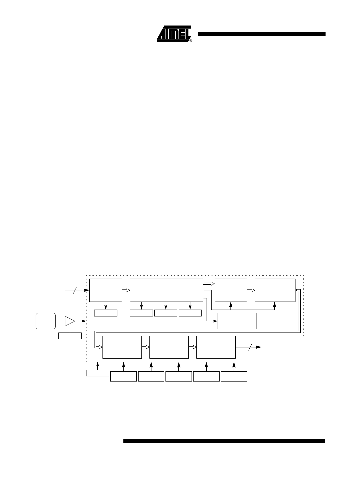
AT8xC51SND1C
14. MP3 Decoder The AT8xC51SND1C implement a MPEG I/II audio layer 3 decoder better known as
e
MP3 decoder.
In MPEG I (ISO 11172-3) three layers of compression have been standardized support-
ing three sampli ng frequencies : 48, 44.1, and 32 kH z. Among these la yers, layer 3
allows highest compression rate of about 12:1 while still maintaining CD audio quality.
For example, 3 minutes of CD audio (16-bit PCM, 44.1 k Hz) data, which needs a bout
32M bytes of storage, can be encoded into only 2.7M bytes of MPEG I audio layer 3
data.
In MPEG II (ISO 13818-3), three additional sampling frequencies: 24, 22.05, and 16 kHz
are supported for low bit rates applications.
The AT8xC51SND1C can decode in real-time the MPEG I audio layer 3 encoded data
into a PCM audio data, and also supports MPEG II audio layer 3 additional frequencies.
Additional features are supported by the AT8xC51SND1C MP3 decoder such as volume
control, bass, medium, and treble controls, bass boost effect and a ncillary data
extraction.
14.1 Decoder
14.1.1 Description The C51 core interfaces to the MP3 decoder through nine special function registers:
MP3CON, the MP3 Control register (see Table 12); MP3STA, the MP3 Status register
(see Table 13); MP3DAT, the MP3 Data register (see Table 14); MP3ANC, the Ancillary
Data register (see Table 16); MP3VOL and MP3VOR, the MP3 Volume Left and Right
Control registers (see Table 17 and Table 18); MP3BAS, MP3MED, and MP3TRE, the
MP3 Bass, Medium, and Treble Control register s (see Table 19, Table 20, and
Table 21); and MPCLK, the MP3 Clock Divider register (see Table 22).
Figure 44 shows the MP3 decoder block diagram.
Figure 44. MP3 Decoder Block Diagram
Audio Data
From C51
MP3
CLOCK
8
MPEN
MP3CON.7
1K Bytes
Frame Buffer
MP3DAT
MPxREQ
MP3STA1.n
Anti-Aliasing
MPBBST
MP3CON.6
MP3VOL MP3VOR MP3BAS MP3MED MP3TRE
Header Checker
Huffman Decoder
ERRxxx
MP3STA.5:3
MPFS1:0
MP3STA.2:1
IMDCT
MPVER
MP3STA.0
Dequantizer
Ancillary Buffer
Sub-band
Synthesis
Side Information
MP3ANC
Stereo Processor
Decoded Data
16
To Audio Interfac
64
4109H–8051–01/05

AT8xC51SND1C
14.1.2 MP3 Data The MP3 decoder does not start any frame decoding before having a complete frame in
its input buffer
(1)
. In order to manage the load of MP3 data in the frame buffer, a hardware handshake consisting of data request and data acknowledgment is implemented.
Each time the MP3 decoder needs MP3 data, it sets the MPREQ, MPFREQ and
MPBREQ flags respectively in MP3STA and MP3STA1 registers. MPREQ flag can generate an interrupt if enabled as explained in Section “Interrupt”. The CPU must then load
data in the buffer by writing it through MP3DAT register thus acknowledging the previous request. As shown in Figure 45, the MPFREQ flag remains set while data (i.e a
frame) is requested by the decoder. It is cleared when no more data is requested and
set again when new data are requested. MPBREQ flag toggles at every Byte writing.
Note: 1. The first request after enable, consists in 1024 Bytes of data to fill in the input buffer.
Figure 45. Data Timing Diagram
MPREQ Flag
MPFREQ Flag
MPBREQ Flag
Write to MP3DAT
Cleared when Reading MP3STA
14.1.3 MP3 Clock The MP3 decoder clo ck i s gener ated by di visio n of t he PL L clo ck. The di vision facto r is
given by MPCD4:0 bits in MP3CLK regis ter. Figure 46 shows the MP3 decoder clock
generator and its calculation formula. The MP3 decoder clock frequency depends only
on the incoming MP3 frames.
Figure 46. MP3 Clock Generator and Symbol
PLL
CLOCK
MP3CLK
MPCD4:0
MP3clk
MP3 Decoder Clock
PLLclk
----------------------------=
MPCD 1+
MP3
CLOCK
MP3 Clock Symbol
As soon as the frame header has been decoded and the MPEG version extracted, the
minimum MP3 input frequency must be programmed according to Table 2.
Table 2. M P3 Clock Frequ enc y
MPEG Version Minimum MP3 Clock (MHz)
I21
II 10.5
4109H–8051–01/05
65

AT8xC51SND1C
14.3 Audio Controls
14.3.1 Volume Control The MP3 decoder implements volume control on both right and left channels. The
MP3VOR and MP3VOL registers allow a 32-step volume control according to Table 4.
Table 4. Volume Control
VOL4:0 or VOR4:0 Volume Gain (dB)
00000 Mute
00001 -33
00010 -27
11110 -1.5
11111 0
14.4.1 Equalization Control Sound can be adjusted usin g a 3-ban d equa li ze r: a bass ban d unde r 750 Hz, a mediu m
band from 750 Hz to 3300 Hz and a treble band over 3300 Hz. The MP3BAS, MP3MED,
and MP3TRE registers allow a 32-step gain control in each band according to Table 5.
Table 5. Bass, Medium, Treble Control
BAS4:0 or MED4:0 or TRE4:0 Gain (dB)
00000 - ∞
00001 -14
00010 -10
11110 +1
11111 +1.5
14.5.1 Special Effect The MPBBST bit in MP3CON register allows enabling of a bass boost effect with the following characteristics: gain increase of +9 dB in the frequency under 375 Hz.
14.6 Decoding Errors The three different er rors that can appear during frame proces sing are detailed in the
following sections. All these errors can trigger an interrupt as explained in Section "Interrupt", page 68.
14.6.1 Layer Error The ERRSYN fl ag in M P3STA is set when a n on-supported layer is decoded in the
header of the frame that has been sent to the decoder.
14.6.2 Synchroniza tio n Er ror The ERRS YN flag in MP3STA is set when no synchr onizat ion patter n is found i n the
data that have been sent to the decoder.
14.6.3 CRC Error When the CRC of a frame doe s not match t he one cal culated, the f lag ERRCRC in
MP3STA is set. In this case, depending on the CRCEN bit in MP3CON, the frame is
played or rejected. In both cases, noise may appear at audio output.
66
4109H–8051–01/05
AT8xC51SND1C
14.7 Frame Information The MP3 frame header contains information on the audio data contained in the frame.
These informations is made available in the MP3STA register for you information.
MPVER and MPFS1:0 bits allow decoding of the sampling frequency according to
Table 8. MPVER bit gives the MPEG versi on (2 or 1).
Table 8. MP3 Frame Frequency Sampling
MPVER MPFS1 MPFS0 Fs (kHz)
0 0 0 22.05 (MPEG II)
0 0 1 24 (MPEG II)
0 1 0 16 (MPEG II)
0 1 1 Reserved
1 0 0 44.1 (MPEG I)
1 0 1 48 (MPEG I)
1 1 0 32 (MPEG I)
1 1 1 Reserved
14.9 Ancillary Data MP3 fra mes al so c ontain data bits call ed anc illary da ta. Th ese data a re ma de ava ilable
in the MP3ANC register for each frame. As shown in Figure 47, the ancilla ry data are
available by Bytes when MPANC flag in MP3STA register is set. MPANC flag is set
when the ancillary buffer is not empty (at least one ancillary data is available) and is
cleared only when there is no more ancillary data in the buffer. This flag can generate an
interrupt as expl ained in Sectio n "Interr upt", pa ge 68. Wh en set, soft ware mus t read all
Bytes to empty the ancillary buffer.
Figure 47. Ancillary Data Block Diagram
Ancillary
Data To C51
8
MP3ANC
8
7-Byte
Ancillary Buffer
MPANC
MP3STA.7
4109H–8051–01/05
67
AT8xC51SND1C
14.10 Interrupt
t
E
14.10.1 Description As shown in Figure 48, the MP3 decoder implements five interrupt sources reported in
ERRCRC, ERRSYN, ERRLAY, MPREQ, and MPANC flags in MP3STA register.
All these sources are maskable separately using MSKCRC, MSKSYN, MSKLAY,
MSKREQ, and MSKANC mask bits respectively in MP3CON register.
The MP3 interrupt is enabled by setting EMP3 bit in IEN0 register. This assumes interrupts are globally enabled by setting EA bit in IEN0 register.
All interrupt flags b ut MP REQ an d MP AN C ar e cl eared when reading MP3STA regis ter.
The MPREQ flag is cleared by hardware when no more data is requested (see
Figure 45) and MPANC flag is cleared by hardware when the ancillary buffer becomes
empty.
Figure 48. MP3 Decoder Interrupt System
MPANC
MP3STA.7
MSKANC
MPREQ
MP3STA.6
ERRLAY
MP3STA.5
ERRSYN
MP3STA.4
RRCRC
MP3STA.3
MSKREQ
MP3CON.3
MSKSYN
MP3CON.1
MP3CON.4
MSKLAY
MP3CON.2
MSKCRC
MP3CON.0
MP3 Decoder
Interrupt Reques
EMP3
IEN0.5
14.10.2 Management Reading the MP3STA register automatically clears the interrupt flags (acknowledgment)
except the MPREQ and MPANC flag s. This im plies that regist er conte nt must be sa ved
and tested, interrupt flag by interrupt flag to be sure not to forget any interrupts.
68
4109H–8051–01/05
Figure 49. MP3 Interrupt Service Routine Flow
MP3 Decoder
ISR
Read MP3STA
Data Request?
MPFREQ = 1?
Data Request
Handler
AT8xC51SND1C
Write MP3 Data
to MP3DAT
Synchro Error
Handler
Reload MP3 Frame
Through MP3DAT
Ancillary Data?
MPANC = 1?
Sync Error?
ERRSYN = 1?
Layer Error?
ERRSYN = 1?
(1)
(1)
(1)
CRC Error
Handler
Load New MP3 Frame
Through MP3DAT
Ancillary Data
Handler
Read ANN2:0 Ancillary
Bytes From MP3ANC
Layer Error
Handler
4109H–8051–01/05
Note: 1. Test these bits only if needed (unmasked interrupt).
69

AT8xC51SND1C
14.11 Registers Table 12. MP3CON Register
MP3CON (S:AAh) – MP3 Decoder Control Register
76543210
MPEN MPBBST CRCEN MSKANC MSKREQ MSKLAY MSKSYN MSKCRC
Bit
Number
7MPEN
6 MPBBST
5 CRCEN
4 MSKANC
3MSKREQ
2MSKLAY
1 MSKSYN
Bit
Mnemonic Description
MP3 Decoder Enable Bit
Set to enable the MP3 decoder.
Clear to disable the MP3 decoder.
Bass Boost Bit
Set to enable the bass boost sound effect.
Clear to disable the bass boost sound effect.
CRC Check Enable Bit
Set to enable processing of frame that contains CRC error. Frame is played
whatever the error.
Clear to disable processing of frame that contains CRC error. Frame is skipped.
MPANC Flag Mask Bit
Set to prevent the MPANC flag from generating a MP3 interrupt.
Clear to allow the MPANC flag to generate a MP3 interrupt.
MPREQ Flag Mask Bit
Set to prevent the MPREQ flag from generating a MP3 interrupt.
Clear to allow the MPREQ flag to generate a MP3 interrupt.
ERRLAY Flag Mask Bit
Set to prevent the ERRLAY flag from generating a MP3 interrupt.
Clear to allow the ERRLAY flag to generate a MP3 interrupt.
ERRSYN Flag Mask Bit
Set to prevent the ERRSYN flag from generating a MP3 interrupt.
Clear to allow the ERRSYN flag to generate a MP3 interrupt.
0 MSKCRC
ERRCRC Flag Mask Bit
Set to prevent the ERRCRC flag from generating a MP3 interrupt.
Clear to allow the ERRCRC flag to generate a MP3 interrupt.
Reset Value = 0011 1111b
70
4109H–8051–01/05
AT8xC51SND1C
Table 13. MP3STA Register
MP3STA (S:C8h Read Only) – MP3 Decoder Status Register
76543210
MPANC MPREQ ERRLAY ERRSYN ERRCRC M PFS1 MPFS0 MPVER
Bit
Number
7MPANC
6MPREQ
5 ERRLAY
4 E RRSYN
3 ERRCRC
2 - 1 M PF S1: 0
0 MPVER
Bit
Mnemonic Description
Ancillary Data Available Flag
Set by hardware as soon as one ancillary data is available (buffer not empty).
Cleared by hardware when no more ancillary data is available (buffer empty).
MP3 Data Request Flag
Set by hardware when MP3 decoder request data.
Cleared when reading MP3STA.
Invalid Layer Error Flag
Set by hardware when an invalid layer is encountered.
Cleared when reading MP3STA.
Frame Synchronization Error Flag
Set by hardware when no synchronization pattern is encountered in a frame.
Cleared when reading MP3STA.
CRC Error Flag
Set by hardware when a frame handling CRC is corrupted.
Cleared when reading MP3STA.
Frequency Sampling Bits
Refer to Table 8 for bits description.
MPEG Version Bit
Set by the MP3 decoder when the loaded frame is a MPEG I frame.
Cleared by the MP3 decoder when the loaded frame is a MPEG II frame.
Reset Value = 0000 0001b
4109H–8051–01/05
Table 14. MP3DAT Register
MP3DAT (S:ACh) – MP3 Data Register
76543210
MPD7 MPD6 MPD5 MPD4 MPD3 MPD2 MPD1 MPD0
Bit
Number
7 - 0 MPD7:0
Bit
Mnemonic Description
Input Stream Data Buffer
8-bit MP3 stream data input buffer.
Reset Value = 0000 0000b
71
AT8xC51SND1C
Table 15. MP3STA1 Register
MP3STA1 (S:AFh) – MP3 Decoder Status Register 1
76543210
- - - MPFREQ MPFREQ---
Bit
Number
7 - 5 -
4MPFREQ
3MPBREQ
2 - 0 -
Bit
Mnemonic Description
Reserved
The value read from these bits is always 0. Do not set these bits.
MP3 Frame Data Request Flag
Set by hardware when MP3 decoder request data.
Cleared when MP3 decoder no more request data .
MP3 Byte Data Request Flag
Set by hardware when MP3 decoder request data.
Cleared when writing to MP3DAT.
Reserved
The value read from these bits is always 0. Do not set these bits.
Reset Value = 0001 0001b
Table 16. MP3ANC Register
MP3ANC (S:ADh Read Only) – MP3 Ancillary Data Register
76543210
AND7 AND6 AND5 AND4 AND3 AND2 AND1 AND0
Bit
Number
Bit
Mnemonic Description
7 - 0 AND7:0
Ancillary Data Buffer
MP3 ancillary data Byte buffer.
Reset Value = 0000 0000b
Table 17. MP3 VO L Regi st er
MP3VOL (S:9Eh) – MP3 Volume Left Control Register
76543210
- - - VOL4 VOL3 VOL2 VOL1 VOL0
Bit
Number
7 - 5 -
4 - 0 VOL4:0
Bit
Mnemonic Description
Reserved
The value read from these bits is always 0. Do not set these bits.
Volume Le ft Value
Refer to Table 4 for the left channel volume control description.
Reset Value = 0000 0000b
72
4109H–8051–01/05
AT8xC51SND1C
Table 18. MP3VOR Register
MP3VOR (S:9Fh) – MP3 Volume Right Control Register
76543210
- - - VOR4 VOR3 VOR2 VOR1 VOR0
Bit
Number
7 - 5 -
4 - 0 VOR4:0
Bit
Mnemonic Description
Reserved
The value read from these bits is always 0. Do not set these bits.
Volume Ri ght Value
Refer to T able4 for the right channel volume control description.
Reset Value = 0000 0000b
Table 19. MP3 BA S Regi st er
MP3BAS (S:B4h) – MP3 Bass Control Register
76543210
- - - BAS4 BAS3 BAS2 BAS1 BAS0
Bit
Number
7 - 5 -
4 - 0 BAS4:0
Bit
Mnemonic Description
Reserved
The value read from these bits is always 0. Do not set these bits.
Bass Gain Value
Refer to Table5 for the bass control description.
Reset Value = 0000 0000b
4109H–8051–01/05
Table 20. MP3MED Register
MP3MED (S:B5h) – MP3 Medium Control Register
76543210
- - MED5 MED4 MED3 MED2 MED1 MED0
Bit
Number
7 - 6 -
5-0 MED5:0
Bit
Mnemonic Description
Reserved
The value read from these bits is always 0. Do not set these bits.
Medium Gain Value
Refer to T able5 for the medium control description.
Reset Value = 0000 0000b
73

AT8xC51SND1C
Table 21. MP3TRE Register
MP3TRE (S:B6h) – MP3 Treble Control Register
76543210
- - TRE5 TRE4 TRE3 TRE2 TRE1 TRE0
Bit
Number
7 - 6 -
5-0 TRE5:0
Bit
Mnemonic Description
Reserved
The value read from these bits is always 0. Do not set these bits.
Treble Gain Value
Refer to T able5 for the treble control description.
Reset Value = 0000 0000b
Table 22. MP3CLK Register
MP3CLK (S:EBh) – MP3 Clock Divider Register
76543210
- - - MPCD4 MPCD3 MPCD2 MPCD1 MPCD0
Bit
Number
7 - 5 -
4-0 MPCD4:0
Bit
Mnemonic Description
Reserved
The value read from these bits is always 0. Do not set these bits.
MP3 Decoder Clock Divider
5-bit divider for MP3 decoder clock generation.
Reset Value = 0000 0000b
74
4109H–8051–01/05
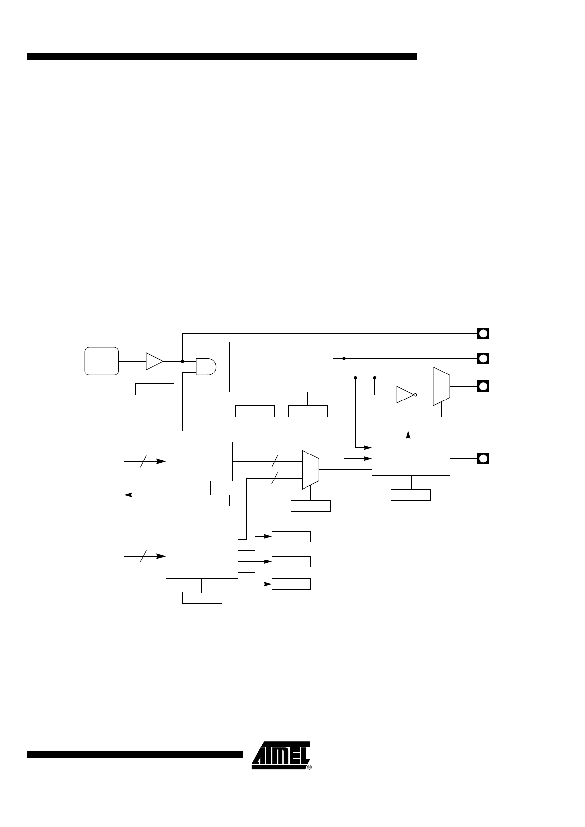
AT8xC51SND1C
T
15. Audio Output
Interface
The AT8xC51SND1C i mplemen t an audio ou tput inte rfac e allow ing t he aud io bitstrea m
to be output in various format s. It is compa tible wit h right an d left jus tificatio n PCM an d
2
I
S formats and thanks to the on-chip PLL (see Section “Clock Controller”, page 12)
allows connection of almost all of the commercial audio DAC families available on the
market.
The audio bitstream can be from 2 different types:
• The MP3 decoded bitstream coming from the MP3 decoder for playing songs.
• The audio bitstream coming from the MCU for outputting voice or sounds.
15.1 Description The C51 core interfaces to th e audio interfac e through f ive sp ecial func tion re gisters:
AUDCON0 and AUDCON1, the Audio Control registers (see Tab le 11 and Table 12);
AUDSTA, the Audio Status register (see Table 13); AUDDAT, the Audio Data register
(see Table 14); and AUDCLK, the Audio Clock Divider register (see Table 15).
Figure 50 shows the audio interface block diagram, blocks are detailed in the following
sections.
Figure 50. Audi o Interface Block Diagram
SCLK
AUD
CLOCK
AUDEN
AUDCON1.0
Data Ready
Clock Generator
HLR
AUDCON0.0
DSIZ
AUDCON0.1
0
1
POL
AUDCON0.2
DCLK
DSEL
Audio Data
From MP3
Decoder
Sample
Request To
MP3 Decoder
Audio Data
From C51
16
MP3 Buffer
DRQEN
AUDCON1.6
16
16
0
1
SRC
AUDCON1.7
Data Converter
JUST4:0
AUDCON0.7:3
DOU
SREQ
8
Audio Buffer
AUDDAT
AUDSTA.7
UDRN
AUDSTA.6
AUBUSY
DUP1:0
AUDCON1.2:1
AUDSTA.5
4109H–8051–01/05
75

AT8xC51SND1C
15.2 Clock Generator The audio interface clock is generated by division of the PLL clock. The division factor is
given by AUCD4:0 bits in CLKAUD register. Figure51 shows the audio interface clock
generator and its calculation formula. The audio interface clock frequency depends on
the incoming MP3 frames and the audio DAC used.
Figure 51. Audio Clock Generator and Symb ol
PLL
CLOCK
AUDCLK
AUCD4:0
AUDclk
Audio Interface Clock
PLLclk
---------------------------=
AUCD1+
AUD
CLOCK
Audio Clock Symbol
As soon as audio interface is enabled by setting AUDEN bit in AUDCON1 register, the
master clock generated by the PL L is out put on the S CLK pin which i s the DAC sy stem
clock. This clock is output at 256 or 384 times the sampling frequency depending on the
DAC capabilities. HLR bit in AUDCON0 register mu st be set according to this rate for
properly generating the audio bit clock on the DCLK pin and the word selection clock on
the DSEL pin. These clocks are not generated when no data is available at the data
converter input.
For DAC compatibilit y, the bit cl ock freque ncy is prog ramma ble for o utputti ng 16 bi ts or
32 bits per channel using the DSIZ bit in AUDCON0 register (see Section "Data Converter", page 76 ), and the word selec tion sign al is progr ammable fo r outputting left
channel on low or high level according to POL bit in AUDCON0 register as shown in
Figure 52.
Figure 52. DSEL Output Polarity
POL = 0
Left Channel Right Channel
POL = 1
Left Channel Right Channel
15.3 Data Converter The data co nv er ter bl oc k converts the audio str eam in put f ro m th e 16 -b it p aral lel form at
to a serial format. For accepting all PCM formats and I
AUDCON0 register are used to shift the data output point. As shown in Figure 53, these
bits allow MSB justification by setting JUST4:0 = 00000, L SB justification by setting
JUST4:0 = 10000, I
2
S Justification by setting JUST4:0 = 00001, a nd more than 16-bit
LSB justification by filling the low significant bits with logic 0.
2
S format, JUST4:0 bits in
76
4109H–8051–01/05

Figure 53. Audio Output Format
AT8xC51SND1C
DSEL
DCLK
DOUT
DSEL
DCLK
DOUT
DSEL
DCLK
DOUT
DSEL
DCLK
DOUT
DSEL
DCLK
DOUT
Left Channel Right Channel
1 2 3 13 14 15 16
MSB
LSB B14 MSBLSB B14B1 B1
2
S Format with DSIZ = 0 and JUST4:0 = 00001.
I
Left Channel Right Channel
1 2 3 17 18 32
MSB
2
S Format with DSIZ = 1 and JUST4:0 = 00001.
I
Left Channel Right Channel
1 2 3 13 14 15 16
B14
MSB B1 B15MSB B1LSB LSB
MSB/LSB Justified Format with DSIZ = 0 and JUST4:0 = 00000.
Left Channel Right Channel
11618 32
115 3032
MSB B16
17 31
MSB B14 LSBB1 MSB B14 LSBB1
16-bit LSB Justified Format with DSIZ = 1 and JUST4:0 = 10000.
Left Channel Right Channel
16 31
B21B1 LSB
18-bit LSB Justified Format with DSIZ = 1 and JUST4:0 = 01110.
1 2 3 13 14 15 16
1 2 3 17 18 32
LSBB14 MSBLSB B14
1 2 3 13 14 15 16
1161817 31
15 30 3216 31
MSB B16
B2 B1 LSB
32
The data converter receives its audio stream from 2 sources selected by the SRC bit in
AUDCON1 register. When cleared, the audio stream comes from the MP3 decoder (see
Section “MP3 Deco der”, pag e 64) for so ng play ing. Whe n se t, the audio stream is coming from the C51 core for voice or sound playing.
As soon as first a udio d ata is inpu t to the data conve rter, it e nables th e cl ock gene rator
for generating the bit and word clocks.
15.4 Audio Buffer In voice or sound playing mode, the audio st ream come s from the C51 cor e thro ugh an
audio buffer. The data is in 8-bit format and is sampled at 8 kHz. The audio buffer
adapts the sample format and rate. The sample format is extended to 16 bits by filling
the LSB to 00h. Rate is adapted to the DAC rate by duplicating the data using DUP1:0
bits in AUDCON1 register according to Table 5.
The audio buffer interfa ces to the C51 c ore th r ough thr ee fla gs: the s am pl e requ es t fla g
(SREQ in AUDSTA register), the under-run flag (UNDR in AUDSTA register) and the
busy flag (AUBUSY in AUDSTA register). SREQ and UNDR can generate an interrupt
request as explained in Sec ti on "In ter ru pt R eque st ", p age 78. The buffer size is 8 Bytes
large. SREQ i s set when the samp les numb er switc hes f rom 4 to 3 an d r eset when the
samples number switches from 4 to 5; UNDR is set when the buffer becomes empty signaling that the audio interface ran out of samples; and AUBUSY is set when the buffer is
full.
4109H–8051–01/05
77

AT8xC51SND1C
Table 5. Sample Duplication Factor
t
t
DUP1 DUP0 Factor
0 0 No sample duplication, DAC rate = 8 kHz (C51 rate).
0 1 One sample duplication, DAC rate = 16 kHz (2 x C51 rate).
1 0 2 samples duplication, DAC rate = 32 kHz (4 x C51 rate).
1 1 Three samples duplication, DAC rate = 48 kHz (6 x C51 rate).
15.6 MP3 Buffer In song playing mo de, the audio stream comes f ro m t he MP3 de co der t hr oug h a buf fer .
The MP3 buffer is used to store the d ecoded MP3 data a nd interfaces to the dec oder
through a 16-bit data input and data request signal. This signal asks for data when the
buffer has enough space to receive new data. Data request is condit ioned by the
DREQEN bit in AUDCON1 regi ster. When set, the buffe r requests data to the MP3
decoder. When clear ed n o m or e d ata is requ es ted but dat a ar e out put unti l the buff er is
empty. This bit can be used to suspend the audio generation (pause mode).
15.7 Interrupt Request The audio interrup t request ca n be gener ated by 2 so urces whe n in C51 audio mod e: a
sample request when SREQ fl ag in AUDST A regi st er is set to lo gi c 1, an d an un der -ru n
condition when UDRN fl ag in AUDS TA register is set to l ogic 1. B oth sources can be
enabled separatel y by masking one of th em using the MSREQ a nd MUDRN bits in
AUDCON1 register. A global enable of the audio interface is provided by setting the
EAUD bit in IEN0 register.
The interrupt is requested each time one of the 2 sources is set to one. The source flags
are cleared by writing some data in the audio buffer through AUDDAT, but the globa l
audio interrupt flag is cleared b y hardware when the interrupt se rvice routine is
executed.
Figure 54. Audio Interface Interrupt System
UDRN
AUDSTA.6
SREQ
AUDSTA.7
MUDRN
AUDCON1.4
EAUD
IEN0.6
MSREQ
AUDCON1.5
Audio
Interrup
Reques
15.8 MP3 Song Playing In MP3 song playing mod e, the operations to do are to configure the PL L a nd th e a udi o
interface according to the DAC s elected. Th e audio clo ck is progr ammed to generate
the 256·Fs or 384·Fs as explained in Section "Clock Generator", page 76. Figure 55
shows the configuration flow of the audio interface when in MP3 song mode.
78
4109H–8051–01/05

Figure 55. MP3 Mode Audio Configuration Flow
MP3 Mode
Configuration
Program Audio Clock
AT8xC51SND1C
Enable DAC System
Clock
AUDEN = 1
Configure Interface
JUST4:0 = XXXXXb
15.9 Voice or Sound
Playing
In voice or sound playing mode, the operations r equired are to configure the PLL and
the audio interface according to the DAC selected. The audio clock is programmed to
generate the 256·Fs or 38 4·Fs as for the MP3 playing mode. The data fl ow sent by the
C51 is then regulated by interrupt and data is loaded 4 Bytes by 4 Bytes. Figure 56
shows the configuration flow of the audio interface when in voice or sound mode.
Figure 56. Voice or Sound Mode Audio Flows
Voice/Song Mode
Configuration
Program Audio Clock
Configure Interface
HLR = X
DSIZ = X
POL = X
JUST4:0 = XXXXXb
DUP1:0 = XX
Wait for DAC
Enable Time
Select Audio
SRC = 1
Load 8 Samples in the
Audio Buffer
HLR = X
DSIZ = X
POL = X
SRC = 0
Wait For
DAC Set-up Time
Enable Data Request
DRQEN = 1
Audio Interrupt
Service Routine
Sample Request?
SREQ = 1?
Load 4 Samples in the
Audio Buffer
Under-run Condition
1
Enable DAC System
Clock
AUDEN = 1
Enable Interrupt
Set MSREQ & MUDRN
EAUD = 1
1
Note: 1. An under-run occurrence signifies that C51 core did not respond to the previous sample request interrupt. It may never
occur for a correct voice/sound generation. It is the user’s responsibility to mask it or not.
79
4109H–8051–01/05

AT8xC51SND1C
15.10 Registers Table 11. AUDCON0 Register
AUDCON0 (S:9Ah) – Audio Interface Control Register 0
76543210
JUST4 JUST3 JUST2 JUS T 1 JUST0 POL DSIZ HLR
Bit
Number
7 - 3 JUST4:0
2POL
1DSIZ
0HLR
Bit
Mnemonic Description
Audio Stream Justification Bits
Refer to Section "Data Converter", page 76 for bits description.
DSEL Signal Output Polarity
Set to output the left channel on high level of DSEL output (PCM mode).
Clear to output the left channel on the low level of DSEL output (I
Audio Data Size
Set to select 32-bit data output format.
Clear to select 16-bit data output format.
High/Low Rate Bit
Set by software when the PLL clock frequency is 384·Fs.
Clear by software when the PLL clock frequency is 256·Fs.
2
S mode).
Reset Value = 0000 1000b
Table 12. AUDCON1 Register
AUDCON1 (S:9Bh) – Audio Interface Control Register 1
76543210
SRC DRQEN MSREQ MUDRN - DUP1 DUP0 AUDEN
Bit
Number
Bit
Mnemonic Description
80
7SRC
6 DRQEN
5MSREQ
4 MUDRN
3-
2 - 1 DUP1:0
0 AUDEN
Audio Source Bit
Set to select C51 as audio source for voice or sound playing.
Clear to select the MP3 decoder output as audio source for song playing.
MP3 Decoded Data Request Enable Bit
Set to enable data request to the MP3 decoder and to start playing song.
Clear to disable data request to the MP3 decoder.
Audio Sample Request Flag Mask Bit
Set to prevent the SREQ flag from generating an audio interrupt.
Clear to allow the SREQ flag to generate an audio interrupt.
Audio Sample Under-run Flag Mask Bit
Set to prevent the UDRN flag from generating an audio interrupt.
Clear to allow the UDRN flag to generate an audio interrupt.
Reserved
The value read from this bit is always 0. Do not set this bit.
Audio Duplication Factor
Refer to Table 5 for bits description.
Audio Interface Enable Bit
Set to enable the audio interface.
Clear to disable the audio interface.
Reset Value = 1011 0010b
4109H–8051–01/05
AT8xC51SND1C
Table 13. AUDSTA Register
AUDSTA (S:9Ch Read Only) – Audio Interface Status Register
76543210
SREQ UDRN AUBUSY -----
Bit
Number
7SREQ
6 UDRN
5 AUBUSY
4 - 0 -
Bit
Mnemonic Description
Audio Sample Request Flag
Set in C51 audio source mode when the audio interface request samples (buffer
half empty). This bit generates an interrupt if not masked and if enabled in IEN0.
Cleared by hardware when samples are loaded in AUDDAT.
Audio Sample Under-run Flag
Set in C51 audio source mode when the audio interface runs out of samples
(buffer empty). This bit generates an interrupt if not masked and if enabled in
IEN0.
Cleared by hardware when samples are loaded in AUDDAT.
Audio Interface Busy Bit
Set in C51 audio source mode when the audio interface can not accept more
sample (buffer full).
Cleared by hardware when buffer is no more full.
Reserved
The value read from these bits is always 0. Do not set these bits.
Reset Value = 1100 0000b
Table 14. AUDDAT Register
AUDDAT (S:9Dh) – Audio Interface Data Register
76543210
AUD7 AUD6 AUD5 AUD4 AUD3 AUD2 AUD1 AUD0
4109H–8051–01/05
Bit
Number
7 - 0 AUD7:0
Bit
Mnemonic Description
Audio Data
8-bit sampling data for voice or sound playing.
Reset Value = 1111 1111b
Table 15. AUDCLK Register
AUDCLK (S:ECh) – Audio Clock Divider Register
76543210
- - - AUCD4 AUCD3 AUCD2 AUCD1 AUCD0
Bit
Number
7 - 5 -
4 - 0 AUCD4:0
Bit
Mnemonic Description
Reserved
The value read from these bits is always 0. Do not set these bits.
Audio Clock Divider
5-bit divider for audio clock generation.
Reset Value = 0000 0000b
81

AT8xC51SND1C
16. Universal Serial
Bus
The AT8xC51SND1C imp lements a US B device contr oller supp orting full speed data
transfer. In addition to the default control endpoint 0, it provides 2 other endpoints, which
can be configured in control, bulk, interrupt or isochronous modes:
• Endpoint 0: 32-Byte FIFO, default control endpoint
• Endpoint 1, 2: 64-Byte Ping-pong FIFO,
This allows the firmware to be developed conforming to most USB device classes, for
example:
• USB Mass Storage Class Bulk-only Transport, Revision 1.0 - September 31, 1999
• USB Human Interface Device Class, Version 1.1 - April 7, 1999
• USB Device Firmware Upgrade Class, Revision 1.0 - May 13, 1999
16.0.1 USB Mass Storage
Class Bulk-Only Transport
16.0.2 USB Device Firmware
Upgrade (DFU)
Within the Bulk -only fram ework, the Control endpoin t is only use d to transp ort classspecific and standard USB requests for device set-up and configuration. One Bulk-out
endpoint is used to transport commands and data from the host to the device. One Bulk
in endpoint is used to transport status and data from the device to the host.
The following AT8xC51SND1C configuration adheres to those requirements:
• Endpoint 0: 32 Bytes, Control In-Out
• Endpoint 1: 64 Bytes, Bulk-in
• Endpoint 2: 64 Bytes, Bulk-out
The USB Device Fir mware Upd ate (DFU ) proto col can b e used to upgrade th e on-chi p
Flash memory of the AT89C51SND1C. This allows installing product enhancements
and patches to devices that are already in the field. 2 different configurations and
descriptor sets are used to support DFU functions. The Run-Time configuration co-exist
with the usual functions of the device, which is USB Mass Storage for AT89C51SND1C.
It is used to initiate DFU from the normal operating mode. The DFU configuration is
used to perform the firmware update after device re-configuration and USB reset. It
excludes any other function. Only the default control pipe (endpoint 0) is used to support
DFU services in both configurations.
The only possible value for the MaxPacketSize in the DFU configuration is 32 Bytes,
which is the size of the FIFO implemented for endpoint 0.
82
4109H–8051–01/05
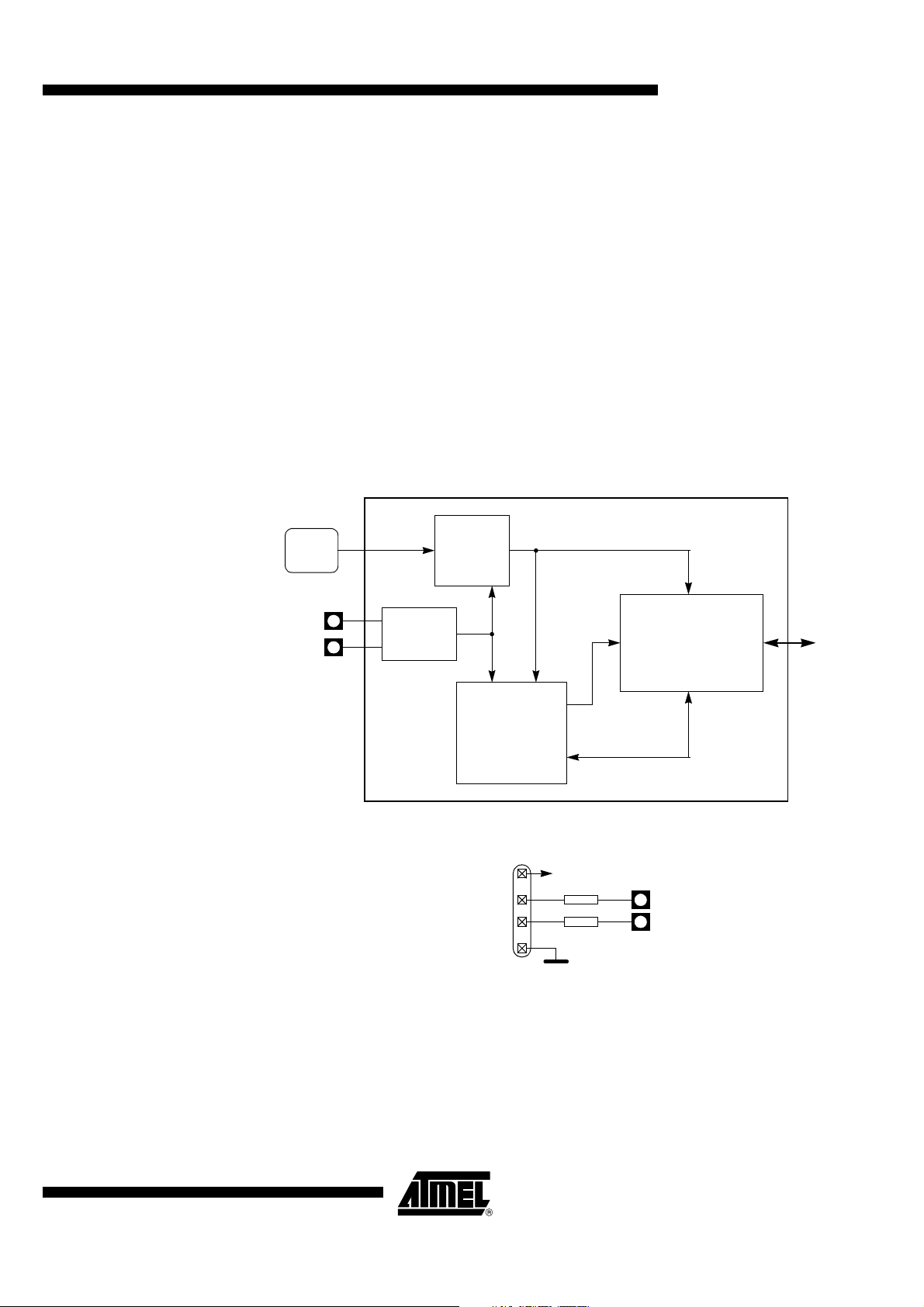
AT8xC51SND1C
e
16.1 Description The USB device controller pro vides the har dware that th e AT8xC51SN D1C needs to
interface a USB link to a data flow stored in a double port memory.
It requires a 48 MHz referenc e cloc k provi de d by the cl oc k c ont ro ller as de tail ed in Se c-
tion "Clock Controlle r", pa ge 8 3. This c lock is use d to gen er ate a 12 MHz Full Spe ed bi t
clock from the received USB differential data flow and to transmit data according to full
speed USB device tolerance. Clock re covery is d one by a Digital Phase Loc ked Loop
(DPLL) block.
The Serial Interface Engine (SIE) block performs NRZI encoding and decoding, bit stuffing, CRC generation and checking, and the serial-parallel data conversion.
The Universal Functio n Interface (UFI) con trols the in terfac e betwee n the data flow and
the Dual Port RAM, but also the interface with the C51 core itself.
Figure 59 shows how to connect the AT8xC51SND1C to the USB connector. D+ and Dpins are connected through 2 termination resistors. Value of these resistors is detailed in
the section “DC Characteristics”.
Figure 57. USB Device Controller Block Diagram
USB
CLOCK
D+
D-
48 MHz 12 MHz
DPLL
USB
Buffer
Figure 58. USB Connection
VBUS
D+
GND
SIE
D-
To Powe r Supply
R
USB
R
USB
VSS
D+
D-
UFI
To/From
C51 Cor
16.1.1 Clock Controller The USB controller clock is generated by division of the PLL clock. The division factor is
given by USBCD1:0 bits in USBCLK register (see Table 24). Figure 59 shows the USB
controller clock g enerator and its calc ulation form ula. The USB controller clock frequency must always be 48 MHz.
83
4109H–8051–01/05
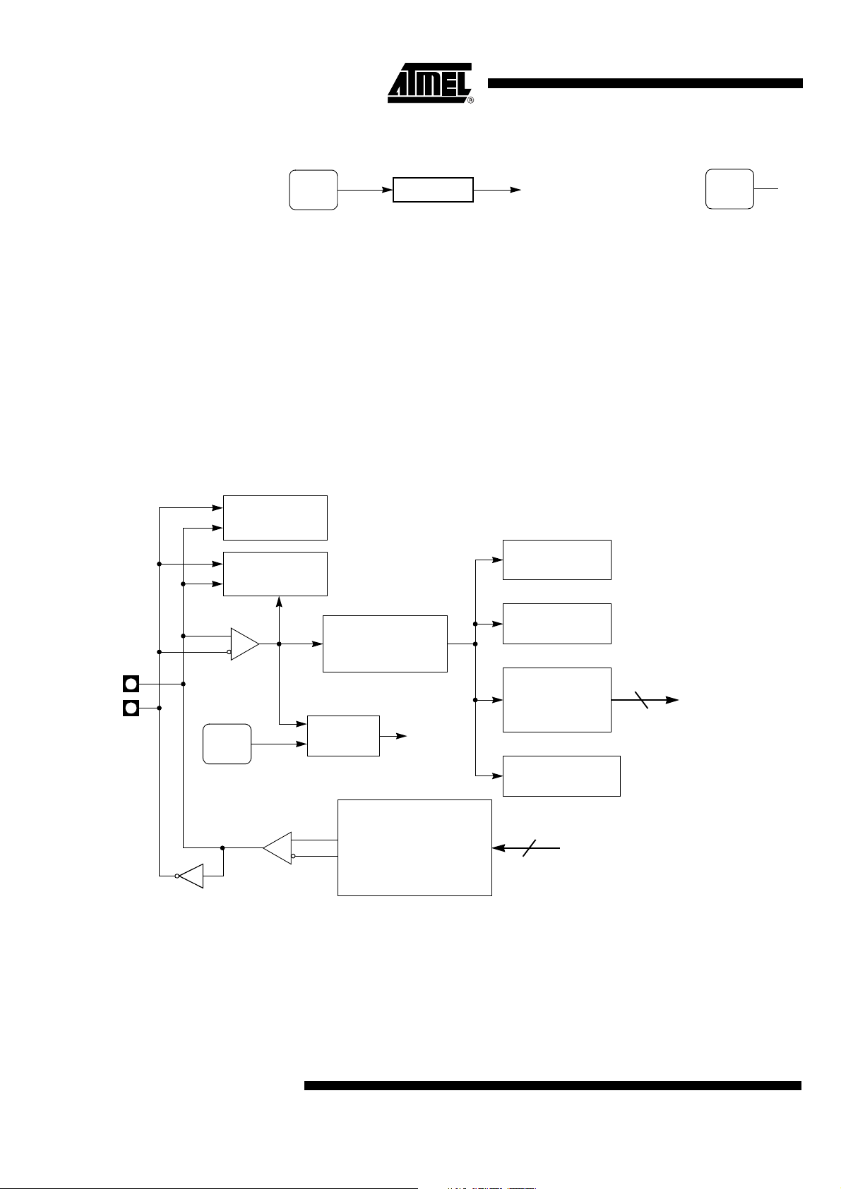
AT8xC51SND1C
Figure 59. USB Clock Generator and Symbol
t
16.1.2 Serial Interface Engine
(SIE)
Figure 60. SIE Block Diagram
PLL
CLOCK
USBCLK
USBCD1:0
USBclk
The SIE performs the following functions:
• NRZI data encoding and decoding.
• Bit stuffing and unstuffing.
• CRC generation and checking.
• ACKs and NACKs automatic generati on .
• TOKEN type identifying.
• Address checking.
• Clock recovery (using DPLL).
End of Packet
Detector
Start of Packet
Detector
48 MHz USB Clock
PLLclk
--------------------------------=
USBCD 1+
SYNC Detector
USB
CLOCK
USB Clock Symbol
D+
D-
USB
CLOCK
48 MHz
NRZI ‘ NRZ
Bit Unstuffing
Packet Bit Counter
Clock
Recover
SysClk
(12 MHz)
USB Pattern Generator
Parallel to Serial Converter
Bit Stuffing
NRZI Converter
CRC16 Generator
PID Decoder
Address Decoder
Serial to Parallel
Converter
CRC5 & CRC16
Generator/Check
8
Data In
8
Data Ou
84
4109H–8051–01/05
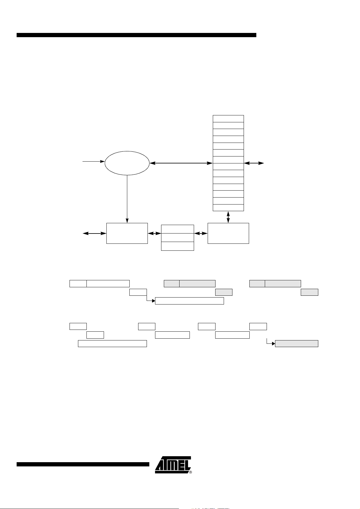
AT8xC51SND1C
e
1
e
16.1.3 Function Interface Unit
(UFI)
Figure 61. UFI Block Diagram
2 MHz DPLL
To/From SIE
The Function Interface Unit provides the interface between the AT8xC51SND1C and
the SIE. It manages transactions at the packet level with minimal intervention from the
device firmware, which reads and writes the endpoint FIFOs.
Figure 62 shows typica l USB IN and OUT transa ctions reporti ng the split in the hardware (UFI) and software (C51) load.
USBCON
USBADDR
USBINT
USBIEN
UEPNUM
Transfer
Control
FSM
Endpoint Control
USB side
Asynchronous Information
Endpoint 2
Endpoint 1
Endpoint 0
UEPCONX
UEPSTAX
UEPRST
UEPINT
UEPIEN
UEPDATX
UBYCTX
UFNUMH
UFNUML
Endpoint Control
C51 side
To/From C51 Cor
Figure 62. USB Typical Transaction Load
OUT Transactions:
HOST
OUT DATA0 (n Bytes)
UFI
C51
IN Transactions:
HOST
UFI
C51
IN
NACK
Endpoint FIFO Write
ACK
OUT DATA1
C51 interrupt
Endpoint FIFO read (n Bytes)
IN
DATA1
IN
NACK
DATA1
OUT DATA1
ACK
ACK
C51 interrupt
Endpoint FIFO writ
4109H–8051–01/05
85
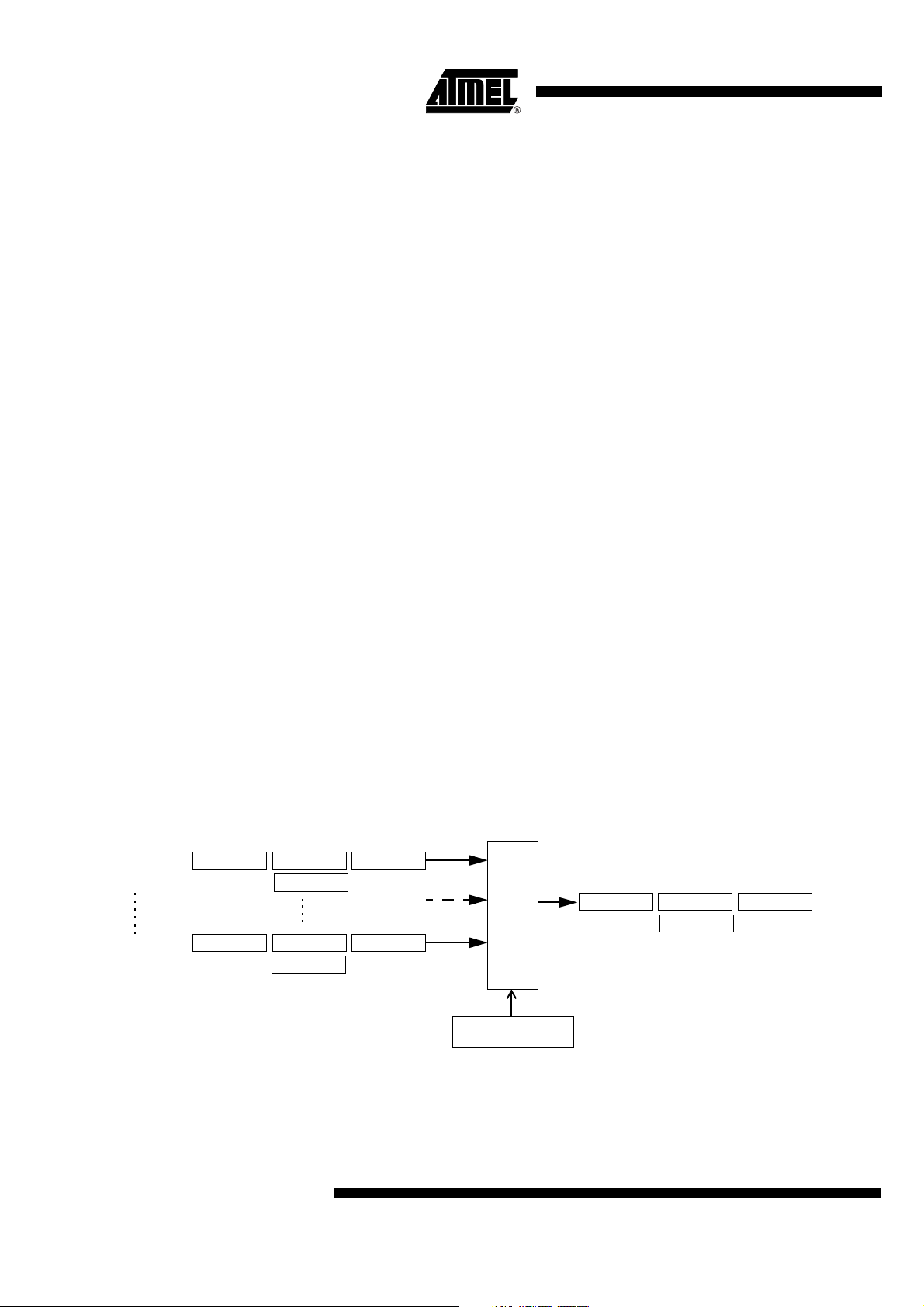
AT8xC51SND1C
16.2 Configuration
16.2.1 General Configuration • USB controller enable
Before any USB tr ansaction, the 48 MHz requi red by the USB c ontroller must be
correctly generated (See “Clock Controller” on page 19).
The USB controller should be then enabled by setting the EUSB bit in the USBCON
register.
• Set address
After a Reset or a USB r eset, th e s oftware has to set the FEN (Function Enable) bit
in the USBADDR register. Thi s action will allo w the USB contr oller to answer to th e
requests sent at the address 0.
When a SET_AD DRES S requ est ha s been r eceiv ed, the USB con trolle r must only
answer to the address defined by the request. The new address should be stored in
the USBADDR register. The FEN bit and the FADDEN bit in the USBCON register
should be set to allow the USB controller to answer only to requests sent at the new
address.
• Set configuration
The CONFG bit in the USBCON register should be set after a
SET_CONFIGURATION request with a non-zero value. Otherwise, this bit should
be cleared.
16.2.2 Endpoint Configuration • Selection of an Endpoint
The endpoint register access is performed using the UEPNUM register. The
registers
–UEPSTAX
– U EPCONX
–UEPDATX
–UBYCTX
Theses registers correspond to the endpoint whose number is stored in the UE P-
NUM register. To select an Endpoint, the firmware has to write the endpoint number
in the UEPNUM register.
Figure 63. Endpoint Selection
Endpoint 0
Endpoint 2
UEPSTA0 UEPCON0 UEPDAT0
UEPSTA2 UEPCON2 UEPDAT2
86
UBYCT0
UBYCT2
0
1
X
2
UEPNUM
SFR Registers
UEPSTAX UEPCONX UEPDATX
UBYCTX
4109H–8051–01/05

AT8xC51SND1C
• Endpoint enable
Before using an endpoint, thi s must be enabled by setting the EPEN bit in the UE PCONX register.
An endpoint which is not enabled won’t answer to any USB request. The Default
Control Endpoint (Endp oint 0) should always be ena bled in order to answer to USB
standard requests.
• Endpoint type configuration
All Standard Endp oin ts can be con figur ed in Contr ol, Bu lk, I nterrupt or Is ochron ous
mode. The Ping-pong Endpoints can be configured in Bulk, Interrupt or Isochronous
mode. The configuration of an e ndpoint is performed by setting the field EPTYPE
with the following values:
– Control: EPTYPE = 00b
– Isochronous:EPTYPE = 01b
– Bulk: EPTYPE = 10b
– Interrupt: EPTYPE = 11b
The Endpoint 0 i s the Defa ult Contr ol Endpo int an d sh ould always be c onfig ured in
Control type.
• Endpoint direction configuration
For Bulk, Interrup t and Isochrono us endpoints, th e direction is de fined with the
EPDIR bit of the UEPCONX register with the following values:
– IN: EPDIR = 1b
– OUT: EPDIR = 0b
For Control endpoints, the EPDIR bit has no effect.
• Summary of Endpoint Configuration:
Do not forget to select th e cor rect end point nu mber in the UE PNUM reg ister before
accessing endpoint specific registers.
Table 3. Summary of Endpoint Configuration
Endpoint C onfiguration EPEN EPDIR EPTYPE UEPCONX
Disabled 0b Xb XXb 0XXX XXXb
Control 1b Xb 00b 80h
Bulk-in 1b 1b 10b 86h
Bulk-out 1b 0b 10b 82h
Interrupt-In 1b 1b 11b 87h
Interrupt-Out 1b 0b 11b 83h
Isochronous-In 1b 1b 01b 85h
Isochronous-Out 1b 0b 01b 81h
4109H–8051–01/05
87

AT8xC51SND1C
• Endpoint FIFO reset
Before using an endpoint, its FIFO should be reset. This action resets the F IFO
pointer to its original value, resets the B yt e counter of the endpoint (UB YCTX r egister), and resets the data toggle bit (DTGL bit in UEPCONX).
The reset of an endpoi nt FIFO is per formed by sett ing to 1 and resett ing to 0 the
corresponding bit in the UEPRST register.
For example, in or der to res et the Endp oint n umber 2 FIFO , wr ite 00 00 010 0b the n
0000 0000b in the UEPRST register.
Note that the endpoint reset doesn’t reset the bank number for ping-pong endpoints.
16.4 Read/Write Data
FIFO
16.4.1 Read Data FIFO The read access for each OUT endpoint is performed using the UEPDATX register.
After a new valid pack et ha s be en r ec ei ved on an Endpoint, the data a re sto r ed i nto th e
FIFO and the Byte counter of the endpoint is updated (UBYCTX registers). The firmware
has to store the endpoint Byte counter before any access to the endpoint FIFO. The
Byte counter is not updated when reading the FIFO.
To read data from an endpoint, select the correct endpoint number in UEPNUM and
read the UEPDATX register. This action automatically decreases the corresponding
address vector, and the next data is then available in the UEPDATX register.
16.4.2 Write Data FIFO The write access for each IN endpoint is performed using the UEPDATX register.
To write a Byte into an IN endpoint FIFO, select the correct endp oint number in UEP-
NUM and write into the UEPDATX register. The corresponding address vector is
automatically increased, and another write can be carried out.
Warning 1: The Byte counter is not updated.
Warning 2: Do not write more Bytes than supported by the corresponding endpoint.
16.4.3 FIFO Mapping
Figure 64. Endpoint FIFO Configuration
SFR Registers
UBYCTX
Endpoint 0
Endpoint 2
UEPSTA0 UEPCON0 UEPDAT0
UBYCT0
UEPSTA2 UEPCON2 UEPDAT2
UBYCT2
0
X
1
UEPSTAX UEPCONX UEPDATX
2
UEPNUM
88
4109H–8051–01/05
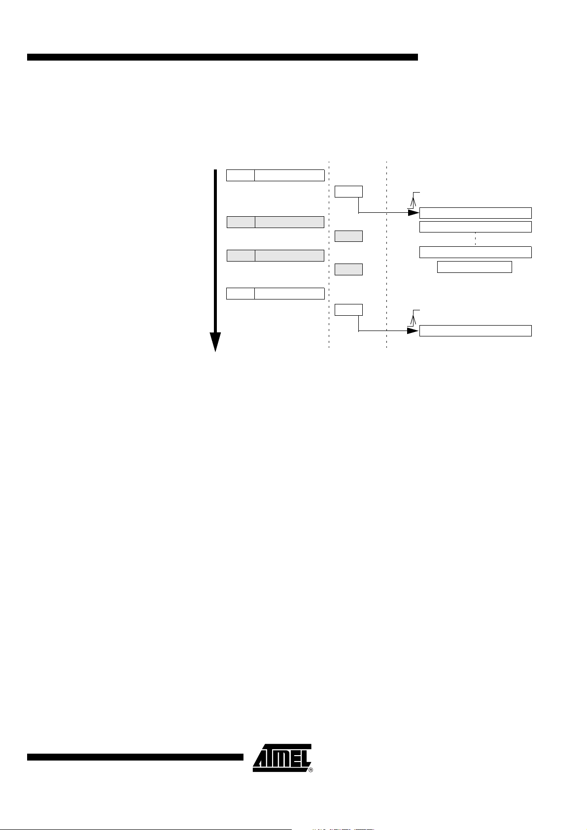
AT8xC51SND1C
16.5 Bulk/Interrupt
Transactions
16.5.1 Bulk/Interrupt OUT
Transactions in Standard
Mode
Bulk and Interrupt transactions are managed in the same way.
Figure 65. Bulk/Interrupt OUT transactions in Standard Mode
HOST UFI
OUT DATA0 (n Bytes)
OUT DATA1
OUT DATA1
DATA1
OUT
ACK
RXOUTB0
NAK
NAK
ACK
RXOUTB0
C51
Endpoint FIFO Read Byte 1
Endpoint FIFO Read Byte 2
Endpoint FIFO Read Byte n
Clear RXOUTB0
Endpoint FIFO Read Byte 1
An endpoint should be fir st e nab le d and co nfi gur ed befo r e being able to receive Bulk or
Interrupt packets.
When a valid O UT pa cket is rece ived o n an en dpoint, the RXO UTB0 bi t is set by the
USB controller. This tr iggers an int errupt i f enabl ed. The fi rmware h as to sel ect the corresponding endpoint, store the number of data Bytes by reading the UBYCTX register. If
the received packe t is a Z L P (Z er o L eng th P ac ket ), the UBYCTX register v alu e i s equal
to 0 and no data has to be read.
When all the endpoint FIFO Bytes have been re ad, the firmware should clear the
RXOUTB0 bit to allow the USB cont roller to a ccept the nex t OUT pack et on this endpoint. Until the RXO UTB0 bit ha s been clear ed by the fi rmware, th e USB cont roller wi ll
answer a NAK handshake for each OUT requests.
If the Host sends more Bytes than supported by the endpoint FIFO, the overflow data
won’t be stored, but the USB controller will consider that the packet is valid if the CRC is
correct and the endpoint Byte counter contains the number of Bytes sent by the Host.
4109H–8051–01/05
89

AT8xC51SND1C
16.5.2 Bulk/Interrupt OUT
Transa ctions in Ping-pong
Mode
Figure 66. Bulk/Interrupt OUT Transactions in Ping-pong Mode
HOST
OUT DATA0 (n Bytes)
DATA1 (m Bytes)
OUT
UFI C51
ACK
RXOUTB0
Endpoint FIFO bank 0 - Read Byte 1
Endpoint FIFO bank 0 - Read Byte 2
OUT DATA0 (p Bytes)
ACK
RXOUTB1
ACK
RXOUTB0
Endpoint FIFO bank 0 - Read Byte n
Clear RXOUTB0
Endpoint FIFO bank 1 - Read Byte 1
Endpoint FIFO bank 1 - Read Byte 2
Endpoint FIFO bank 1 - Read Byte m
Clear RXOUTB1
Endpoint FIFO bank 0 - Read Byte 1
Endpoint FIFO bank 0 - Read Byte 2
Endpoint FIFO bank 0 - Read Byte p
Clear RXOUTB0
An endpoint should be fir st e nab le d and co nfi gur ed befo r e being able to receive Bulk or
Interrupt packets.
When a valid OUT packet is received on the endpoint bank 0, the RXOUTB0 bit is set by
the USB controller. This triggers an interrupt if enabled. The firmware has to select the
corresponding endpoi nt, s tore t he num ber o f data B ytes by readi ng the UBYCT X regi ster. If the received pack et is a ZLP (Zero Len gth Pac ket), the UBYCT X regis ter valu e is
equal to 0 and no data has to be read.
90
When all the endpoint FIFO Bytes have been re ad, the firmware should clear the
RXOUB0 bit to allow the USB contro ller to acc ept the next OUT packet on the endpoi nt
bank 0. This action switches the endpoint bank 0 and 1. Until the RXOUTB0 bit has
been cleared by the firmware, the USB controller will answer a NAK handshake for each
OUT requests on the bank 0 endpoint FIFO.
When a new valid OUT packet is rece ived on the endpo int bank 1, the RXOUT B1 bit is
set by the USB controller. This triggers an interrupt if enabled. The firmware empties the
bank 1 endpoint FIFO before clearing the RXOUTB1 bit. Until the RXOUTB1 bit has
been cleared by the firmware, the USB controller will answer a NAK handshake for each
OUT requests on the bank 1 endpoint FIFO.
The RXOUTB0 and RXO UTB1 bits are, a lter nativ ely, s et b y the USB c ontr oller at e ach
new valid packet receipt.
The firmware has to clear one of these 2 bits after having read all the data FIFO to allow
a new valid packet to be stored in the corresponding bank.
A NAK handshake is sent by the USB co ntroller onl y if the banks 0 and 1 has not bee n
released by the firmware.
4109H–8051–01/05
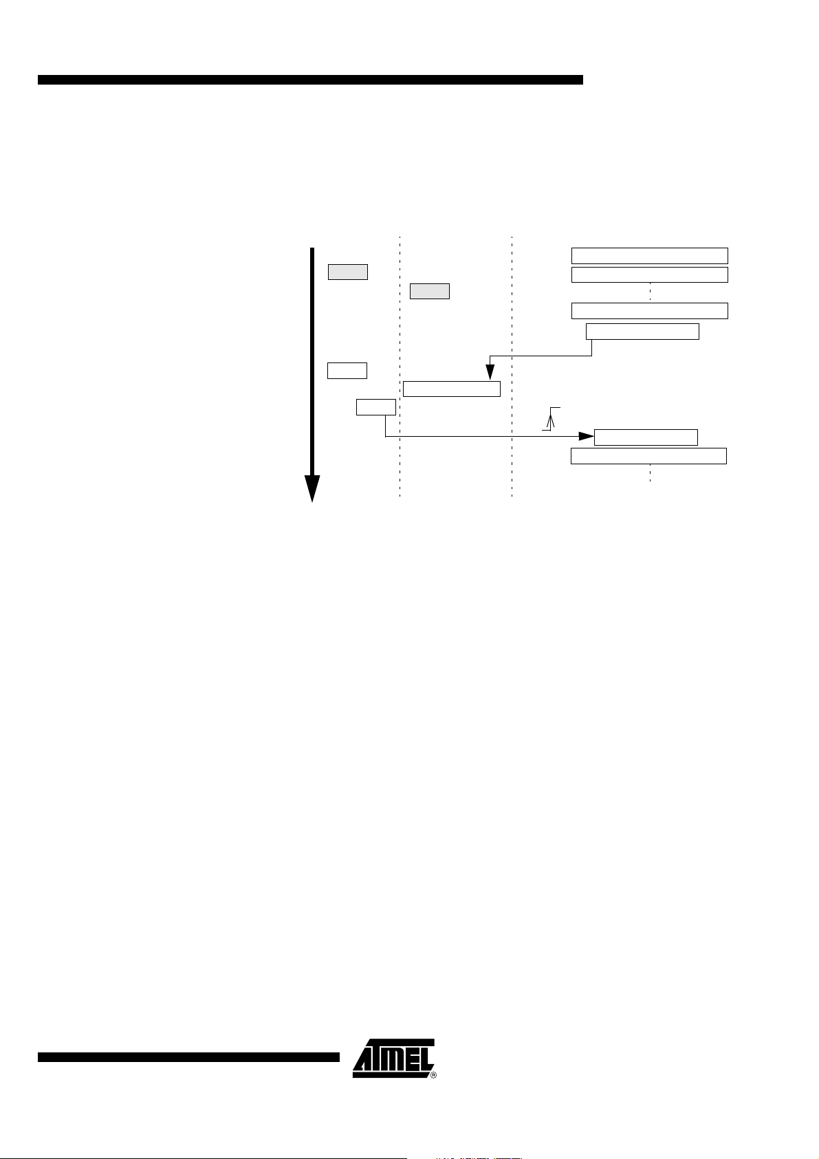
AT8xC51SND1C
If the Host sends more Bytes than supported by the endpoint FIFO, the overflow data
won’t be stored, but the USB controller will consider that the packet is valid if the CRC is
correct.
16.5.3 Bulk/Interrupt IN
Transactions in Standard
Mode
Figure 67. Bulk/Interrupt IN Transactions in Standard Mod e
HOST
IN
IN
ACK
UFI C51
Endpoint FIFO Write Byte 1
Endpoint FIFO Write Byte 2
NAK
Endpoint FIFO Write Byte n
Set TXRDY
DATA0 (n Bytes)
TXCMPL
Clear TXCMPL
Endpoint FIFO Write Byte 1
An endpoint should be first enabled and configured before being able to send Bulk or
Interrupt packets.
The firmware shou ld fill the FIF O with the da ta to be sen t and set th e TXRDY bit in the
UEPSTAX register to allow the USB controller to send the data stored in FIFO at the
next IN request concerning this endpoint. To send a Zero Length Packet, the firmware
should set the TXRDY bit without writing any data into the endpoint FIFO.
Until the TXRDY bit has been set by the firmware, the USB controller will answer a NAK
handshake for each IN requests.
To cancel the sending of this packet, the firmware has to reset the TXRDY bit. The
packet stored in the endpoint FIFO is then cleared and a new packet can be written and
sent.
When the IN packet has been sent and acknowledged by the Host, the TXCMPL bit in
the UEPSTAX register is set by the USB controller. This triggers a USB interrupt if
enabled. The firmware should clear the TXCMPL bit before filling the endpoint FIFO with
new data.
The firmware should never write more Bytes than supported by the endpoint FIFO.
All USB retry mechanisms are automatically managed by the USB controller.
4109H–8051–01/05
91

AT8xC51SND1C
16.5.4 Bulk/Interrupt IN
Transa ctions in Ping-pong
Mode
Figure 68. Bulk/Interrupt IN transactions in Ping-pong mode
HOST
IN
UFI
NACK
C51
Endpoint FIFO bank 0 - Write Byte 1
Endpoint FIFO bank 0 - Write Byte 2
Endpoint FIFO bank 0 - Write Byte n
Set TXRDY
IN
DATA0 (n Bytes)
ACK
TXCMPL
IN
DATA1 (m Bytes)
ACK
TXCMPL
IN
DATA0 (p Bytes)
ACK
Endpoint FIFO bank 1 - Write Byte 1
Endpoint FIFO bank 1 - Write Byte 2
Endpoint FIFO bank 1 - Write Byte m
Clear TXCMPL
Set TXRDY
Endpoint FIFO bank 0 - Write Byte 1
Endpoint FIFO bank 0 - Write Byte 2
Endpoint FIFO bank 0 - Write Byte p
Clear TXCMPL
Set TXRDY
Endpoint FIFO bank 1 - Write Byte 1
An endpoint should be first enabled and configured before being able to send Bulk or
Interrupt packets.
The firmware should fill the FIFO ban k 0 with the data to be sent and set the TXRDY bit
in the UEPSTAX reg ister t o all ow the USB c ontroll er to send the data s tore d in FIF O at
the next IN request concerning the endpoint. The FIFO banks are automatically
switched, and the firmware can immediately write into the endpoint FIFO bank 1.
92
When the IN packet concerning the bank 0 has been sent and acknowledged by the
Host, the TXCMPL bit is set by the USB controller. This triggers a USB interrupt if
enabled. The firmware should clear the TXCMPL bit before filling the endpoint FIFO
bank 0 with new data. The FIFO banks are then automatically switched.
When the IN packet concerning the bank 1 has been sent and acknowledged by the
Host, the TXCMPL bit is set by the USB controller. This triggers a USB interrupt if
enabled. The firmware should clear the TXCMPL bit before filling the endpoint FIFO
bank 1 with new data.
The bank switch is performed by the USB controller each time the TXRDY bit is set by
the firmware. Until the TXRDY bit has been set by th e firmware for an endpo int bank,
the USB controller will answer a NAK handshake for each IN requests concerning this
bank.
Note that in the example above, the firmware clears the Transmit Complete bit
(TXCBulk-outMPL) before setting the Transmit Ready bit (TXRDY). This is done in order
to avoid the firmware to clear at the same time the TXCMPL bit for for bank 0 and the
bank 1.
The firmware should never write more Bytes than supported by the endpoint FIFO.
4109H–8051–01/05

16.6 Control
Transactions
16.6.1 Setup Stage The DIR bit in the UEPSTAX register should be at 0.
Receiving Setup packets is the same as receiving Bulk Out packets, except that the
RXSETUP bit in the UEPSTAX register is set by the USB controller instead of the
RXOUTB0 bit to indicate that an O ut pa cket wi th a S etu p P ID has be en rec eived on th e
Control endpoint. When the RXSETUP bit has been set, all the o ther bits of the UEPSTAX register are cleared and an interrupt is triggered if enabled.
The firmware has to read the Se tup requ est s tored in the Co ntrol endpoi nt FIF O befor e
clearing the RXSETUP bit to free the endpoint FIFO for the next transaction.
AT8xC51SND1C
16.6.2 Data Stage: Control
Endpoint Direction
16.6.3 Status Stage The DIR bit in the UEPSTAX register should be reset at 0 for IN and OUT status stage.
The data stage management is similar to Bulk management.
A Control endpoint is managed by the USB controller as a full-duplex endpoint: IN and
OUT. All othe r endpoi nt typ es are managed as ha lf-dup lex e ndpoint : IN or OUT. T he
firmware has to specify the control endpoint direction for the data stage using the DIR bit
in the UEPSTAX register.
• If the data stage consists of INs, the firmware has to set the DIR bit in the UEPSTAX
register before writing into the FIFO and sending the data by setting to 1 the TXRDY
bit in the UEPSTAX register. The IN transaction is complete when the TXCMPL has
been set by the hardware. The firmware should clear the TXCMPL bit before any
other transaction.
• If the data stage consists of OUTs, the firmware has to leave the DIR bit at 0. The
RXOUTB0 bit is set by hardware when a new valid packet has been received on the
endpoint. The firmware must read the data stored into the FIFO and then clear the
RXOUTB0 bit to reset the FIFO and to allow the next transaction.
To send a STALL handshake, see “STALL Handshake” on page 96.
The status stage management is similar to Bulk management.
• For a Control Write transaction or a No-Data Control transaction, the status stage
consists of a IN Zero Length Packet (see “Bulk/Interrupt IN Transactions in
Standard Mode” on page 91). To send a STALL handshake, see “STALL
Handshake” on page 96.
• For a Control Read transaction, the status stage consists of a OUT Zero Length
Packet (see “Bulk/Interr upt OUT Tra ns act ion s in Sta ndard Mod e” on page 89).
4109H–8051–01/05
93

AT8xC51SND1C
Isochronous Transactions
16.6.4 Isochronous OUT
Transactions in Standard
Mode
16.6.5 Isochronous OUT
Transa ctions in Ping-pong
Mode
An endpoint should be first enabled and configured before being able to receive Isochronous packets.
When an OUT packet is received on an endpoint, the RXOUTB0 bit is set by the USB
controller. This triggers an interrupt if enabled. The firmware has to select the corre
Bulk-outsponding endpoint, store the number of data Bytes by reading the UBYCTX
register. If the received packet is a ZLP (Zero Length Packet), the UBYCTX register
value is equal to 0 and no data has to be read.
The STLCRC bit in the UEPSTAX register is set by the USB controller if the packet
stored in FIFO has a corrupted CRC. This bit is updated after each new packet receipt.
When all the endpoint FIFO Bytes have been re ad, the firmware should clear the
RXOUTB0 bit to allow the USB controller to store the next OUT packet data into the
endpoint FIFO. Until the RX OUTB0 bit has bee n cleared by th e firmwar e, the data sent
by the Host at each OUT transaction will be lost.
If the RXOUTB0 bit is cleared while the Host is sending data, the USB controller will
store only the remaining Bytes into the FIFO.
If the Host sends more Bytes than supported by the endpoint FIFO, the overflow data
won’t be stored, but the USB controller will consider that the packet is valid if the CRC is
correct.
An endpoint should be first enabled and configured before being able to receive Isochronous packets.
When a OUT packet is received on the end point bank 0, the RXO UTB0 bit is set by the
USB controller. This tr iggers an int errupt i f enabl ed. The fi rmware h as to sel ect the corresponding endpoint, store the number of data Bytes by reading the UBYCTX register. If
the received packe t is a Z L P (Z er o L eng th P ac ket ), the UBYCTX register v alu e i s equal
to 0 and no data has to be read.
94
The STLCRC bit in the UEPSTAX register is set by the USB controller if the packet
stored in FIFO has a corrupted CRC. This bit is updated after each new packet receipt.
When all the endpoint FIFO Bytes have been re ad, the firmware should clear the
RXOUB0 bit to allow the USB contr oll er to sto re the nex t OUT pac ket data i nto the endpoint FIFO bank 0. This a ction swi tc hes the end poi nt ba nk 0 an d 1. Un til the RXO UTB 0
bit has been clea red b y the fi rmware, the d ata s ent by the Host o n the bank 0 endp oint
FIFO will be lost.
If the RXOUTB0 bit is cleared while the Host is sending data on the endpoint bank 0, the
USB controller will store only the remaining Bytes into the FIFO.
When a new OUT packet is received on the endpoint bank 1, the RXOUTB1 bit is set by
the USB controller. T his tr iggers an inte rrupt i f enabl ed. The fi rmware emptie s t he bank
1 endpoint FIFO before clearing the RXOUTB1 bit. Until the RXOUTB1 bit has been
cleared by the firmwar e, the data sent by the Host on the bank 1 endp oint FIFO wil l be
lost.
The RXOUTB0 and RXOUTB1 bits are alternatively set by the USB controller at each
new packet receipt.
The firmware has to clear one of these 2 bits after having read all the data FIFO to allow
a new packet to be stored in the corresponding bank.
4109H–8051–01/05

AT8xC51SND1C
If the Host sends more Bytes than supported by the endpoint FIFO, the overflow data
won’t be stored, but the USB controller will consider that the packet is valid if the CRC is
correct.
16.6.6 Isochronous IN
Transactions in Standard
Mode
16.6.7 Isochronous IN
Transa ctions in Ping-pong
Mode
An endpoint should be first enabled and configured before being able to send Isochronous packets.
The firmware shou ld fill the FIF O with the da ta to be sen t and set th e TXRDY bit in the
UEPSTAX register to allow the USB controller to send the data stored in FIFO at the
next IN request concerning this endpoint.
If the TXRDY bit is not set when th e IN reques t occu rs, nothing wi ll be s ent by the USB
controller.
When the IN packet has bee n sent, the TX CMPL bit in the UE PSTAX register is set by
the USB controller. This triggers a USB interrupt if enabled. The firmware should clear
the TXCMPL bit before filling the endpoint FIFO with new data.
The firmware should never write more Bytes than supported by the endpoint FIFO
An endpoint should be first enabled and configured before being able to send Isochro-
nous packets.
The firmware should fill the FIFO ban k 0 with the data to be sent and set the TXRDY bit
in the UEPSTAX reg ister t o all ow the USB c ontroll er to send the data s tore d in FIF O at
the next IN request concerning the endpoint. The FIFO banks are automatically
switched, and the firmware can immediately write into the endpoint FIFO bank 1.
If the TXRDY bit is not set when th e IN reques t occu rs, nothing wi ll be s ent by the USB
controller.
When the IN packet concerning the bank 0 has been sent, the TXCMPL bit is set by the
USB controller. This triggers a USB interrupt if enabled. The firmware should clear the
TXCMPL bit before filli ng t he e ndpo in t F IFO b ank 0 with n ew da ta. T he FI FO b anks are
then automatically switched.
When the IN packet concerning the bank 1 has been sent, the TXCMPL bit is set by the
USB controller. This triggers a USB interrupt if enabled. The firmware should clear the
TXCMPL bit before filling the endpoint FIFO bank 1 with new data.
The bank switch is performed by the USB controller each time the TXRDY bit is set by
the firmware. Until the TXRDY bit has been set by th e firmware for an endpo int bank,
the USB controller won’t send anything at each IN requests concerning this bank.
The firmware should never write more Bytes than supported by the endpoint FIFO.
4109H–8051–01/05
95

AT8xC51SND1C
16.7 Miscellaneous
16.7.1 USB Reset The EORINT bit in the USBINT register is set by hardwar e when a End Of Reset has
been detected o n the USB bus. This trig gers a US B inte rru pt if enab led. The USB c ontroller is still enabled, but all the USB registers are reset by hardware. The firmware
should clear the EORINT bit to allow the next USB reset detection.
16.7.2 STALL Handshake This function is only available for Control, Bulk, and Interrupt endpoints.
The firmware has to set the STALLRQ bit in the UE PSTAX regis ter to send a STAL L
handshake at the next request of the Host on the endpoint selected with the UEPNUM
register. The RXSETUP, TXRDY, TXCMPL, RXOUTB0 and RXOUTB1 bits must be first
resseted to 0. The bit STLCRC is set at 1 by the USB controller when a STALL has been
sent. This triggers an interrupt if enabled.
The firmware should clear the STALLRQ and STLCRC bits after each STALL sent.
The STALLRQ bit is cleared automatically by hardware when a valid SETUP PID is
received on a CONTROL type endpoint.
Important note: when a Clear Halt Feature occurs for an endpoint, the firmware should
reset this endpoint using the UEPRST resgister in order to reset the data toggle
management.
16.7.3 Start of Frame
Detection
16.7.4 Frame Number When receiving a Start Of Frame, the frame number is automatically stored in the
16.7.5 Data Toggle Bit The Data Toggle bit is set by hardware when a DATA0 packet is received and accepted
The SOFINT bit in the USBINT register is set when the USB controller detects a Start Of
Frame PID. This tr igge rs a n int er rupt if ena ble d . The fir mw ar e sho u ld c le ar the SOFINT
bit to allow the next Start of Frame detection.
UFNUML and UFNUMH registers. The CRCOK and CRCERR bits indicate if the CRC of
the last Start Of Frame is valid (CRCOK set a t 1) or co rrupted (C RCERR set a t 1). The
UFNUML and UFNUMH registers are automatically updated when receiving a new Start
of Frame.
by the USB controller and cleared by hardware when a DATA1 packet is received and
accepted by the USB con trolle r. Thi s bit is res et wh en the firmwa re res ets the e ndpoi nt
FIFO using the UEPRST register.
For Control endp oints , each S ETUP tr ansacti on star ts wit h a DATA0 a nd data to gglin g
is then used as for Bulk endpoints until the end of the Data stage (for a control write
transfer). The Status stage completes the data transfer with a DATA1 (for a control read
transfer).
For Isochronous endpoints, the device firmware should ignore the data-toggle.
96
4109H–8051–01/05
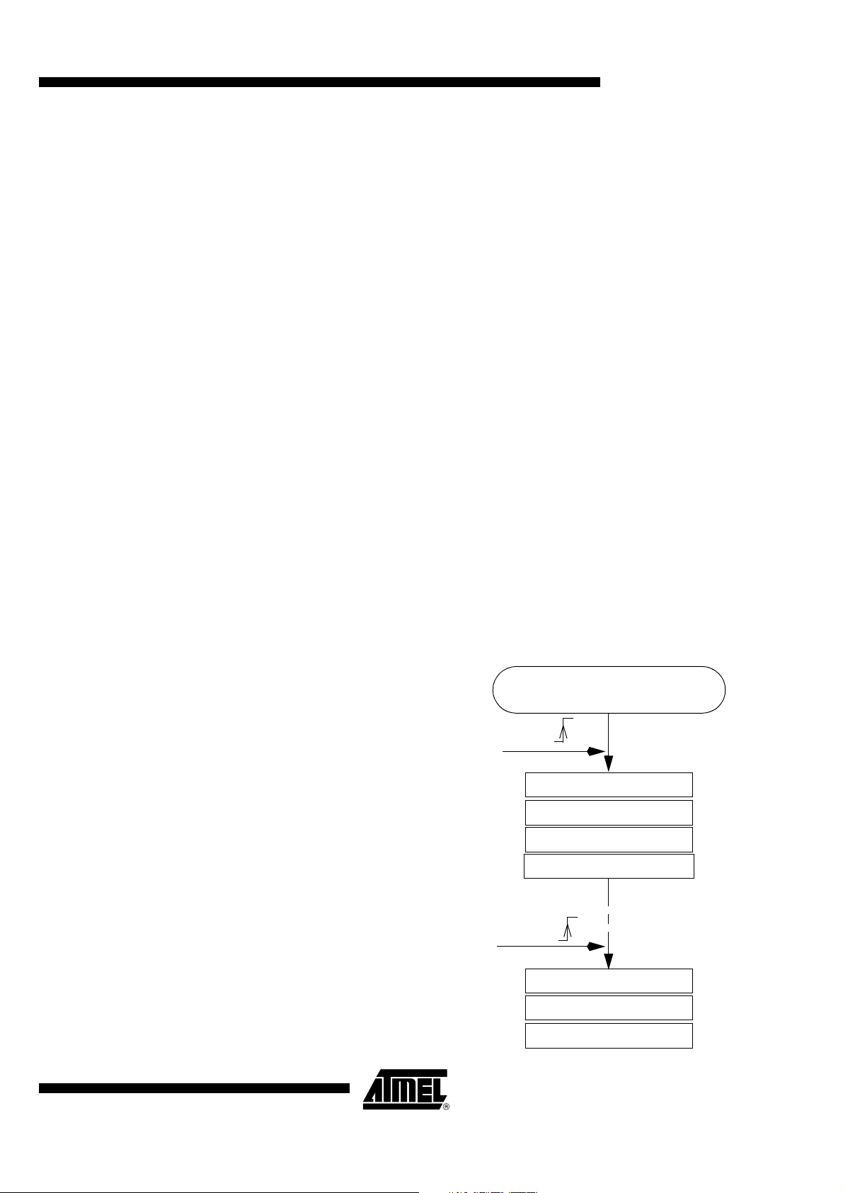
AT8xC51SND1C
Suspend/Resume Management
16.7.6 Suspend The Suspend state can be detected by the USB controller if all the clocks are enabled
and if the USB controller is enabled. The bit SPINT is set by hardware when an idle
state is detected for more than 3 ms. This triggers a USB interrupt if enabled.
In order to reduce current consumption, the firmware can put the USB PAD in idle mode,
stop the clocks and p ut th e C51 in Id le or Power -down mo de. T he Resu me dete ction is
still active.
The USB PAD is put in idle mode when the firmware clear the SPINT bit. In order to
avoid a new suspe nd detecti on 3ms later , the firmwar e has to di sable the USB clock
input using the SUSPCLK bit in the USBCON Register. The USB PAD automatically
exits of idle mode when a wake-up event is detected.
The stop of the 48 MHz clock from the PLL should be done in the following order:
1. Disable of the 48 MHz clock input of the USB controller by setting to 1 the SUS-
PCLK bit in the USBCON register.
2. Disable the PLL by clearing the PLLEN bit in the PLLCON register.
16.7.7 Resume When th e USB cont roll er is in S uspen d state , the Resu me detec tion is a ctive even if al l
the clocks are disabled and if the C51 is in Idle or Power-down mode. The WUPCPU bit
is set by hardware when a non-id le sta te occur s on the US B bus. Thi s trigge rs an in terrupt if enabled. This interrupt wakes up the CPU from its Idle or Power-down state and
the interrupt function is the n executed . The firmw are will fi rst enabl e the 48 MHz generation and then reset to 0 the SUSPCLK bit in the USBCON register if needed.
The firmware has to clear the SPINT bit in the USBINT register before any other USB
operation in order to wake up the USB controller from its Suspend mode.
The USB controller is then re-activated.
Figure 69. Example of a Suspend/Resume Management
USB Controller Init
SPINT
Detection of a SUSPEND State
Clear SPINT
Set SUSPCLK
Disable PLL
microcontroller in Power-down
WUPCPU
Detection of a RESUME State
4109H–8051–01/05
Enable PLL
Clear SUSPCLK
Clear WUPCPU Bit
97
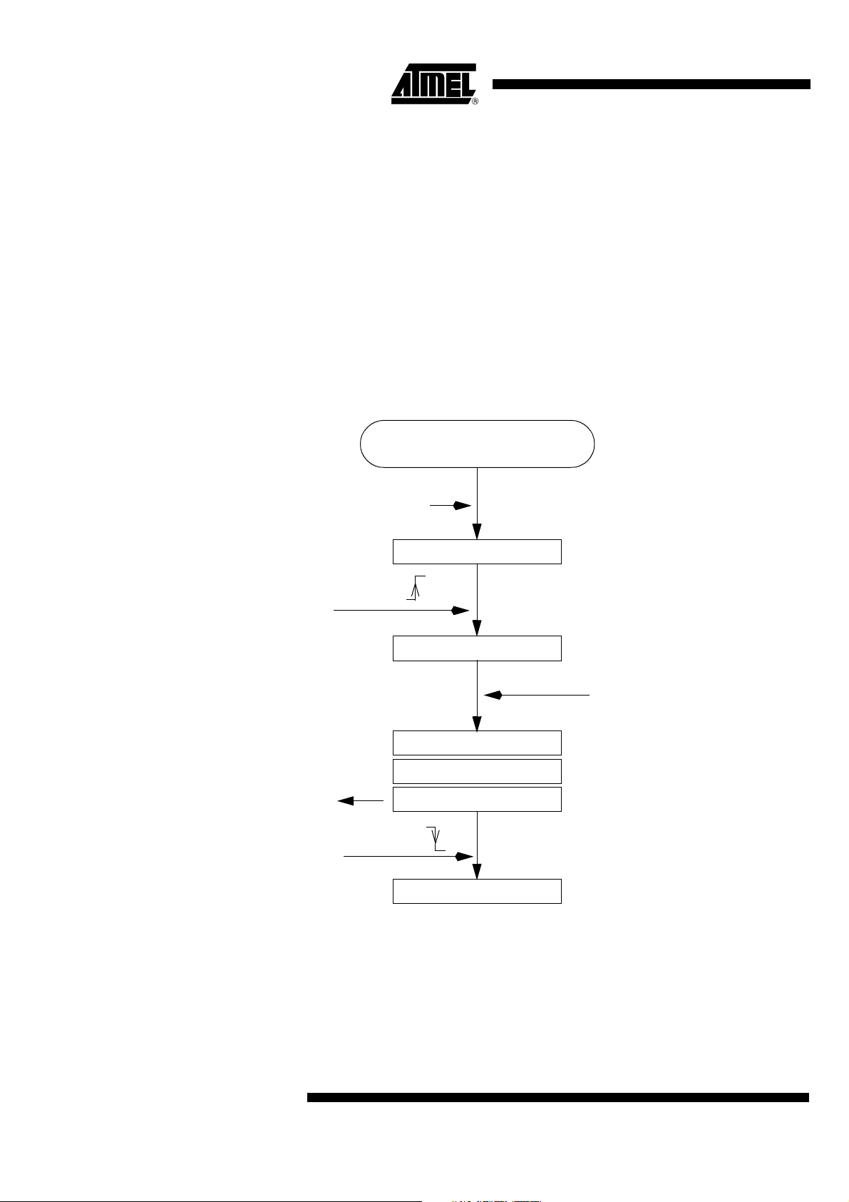
AT8xC51SND1C
16.7.8 Upstream Resume A US B device can be allowed by the Host to send an upstream r esume for Remote
Wake-up purpose.
When the USB controller receives the SET_FEATURE request:
DEVICE_REMOTE_WAKEUP, the fir mware should set to 1 the RMWUPE bit in the
USBCON register to enable this functionality. RMWUPE value should be 0 in the other
cases.
If the device is in SUSPEND mode, the USB controller can send an upstream resume by
clearing first the SPINT bit in the USBINT register and by setting then to 1 the SDRMWUP bit in the USBCON register. The US B controller se ts to 1 the UPRSM bi t in the
USBCON register. All clocks must be enabled first. The Remote Wake is sent only if the
USB bus was in Susp end sta te for at leas t 5ms. When the upstre am resume is completed, the UPRSM bit is reset to 0 by hardware. The firmware should then clear the
SDRMWUP bit.
Figure 70. Example of REMOTE WAKEUP Management
USB Controller Init
SET_FEATURE: DEVICE_REMOTE_WAKEUP
Set RMWUPE
Detection of a SUSPEND state
UPRSM = 1
upstream RESUME sent
SPINT
Suspend Management
need USB resume
enable clocks
Clear SPINT
Set SDMWUP
UPRSM
Clear SDRMWUP
98
4109H–8051–01/05
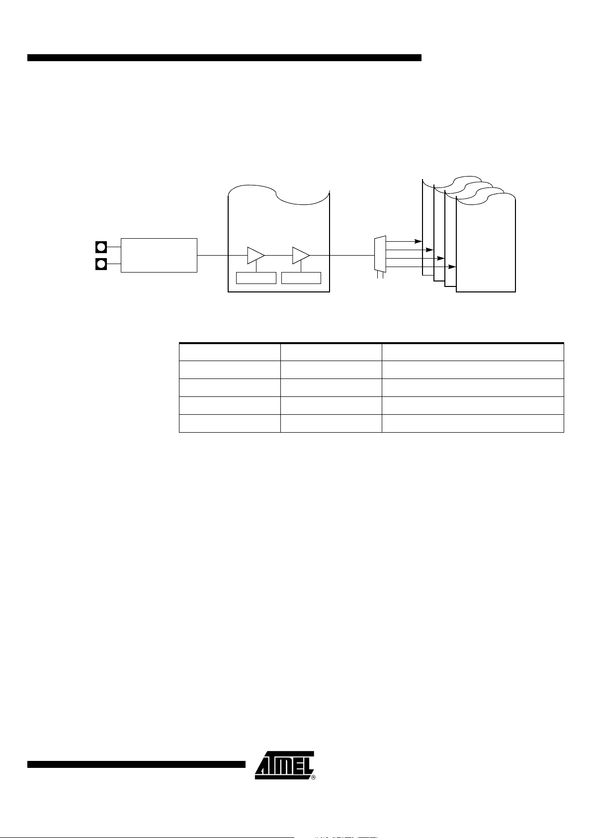
16.8 USB Interrupt
System
AT8xC51SND1C
16.8.1 Interrupt System
Priorities
D+
D-
USB
Controller
Figure 71. USB Interrupt Control System
EUSB
IE1.6
Interrupt Enable Lowest Priority Interrupts
EA
IE0.7
Priority Enable
Table 1. Priority Levels
IPHUSB IPLUSB USB Priority Level
0 0 0..................Lowest
01 1
10 2
1 1 3..................Highest
00
01
10
11
IPH/L
16.8.2 USB Interrupt Control
System
As shown in Figure 72, many events can produce a USB interrupt:
• TXCMPL: Transmitted In Data (Table 16 on page 105). This bit is set by hardware
when the Host accept a In packet.
• RXOUTB0: Received Out Data Bank 0 (Table 16 on page 105). This bit is set by
hardware when an Out packet is accepted by the endpoint and stored in bank 0.
• RXOUTB1: Received Out Data Bank 1 (only for Ping-pong endpoints) (Table 16 on
page 105). This bit is set by hardware when an Out packet is accepted by the
endpoint and stored in bank 1.
• RXSETUP: Received Setup (Table 16 on page 105). This bit is set by hardware
when an SETUP packet is accepted by the endpoint.
• STLCRC: STALLED (only for Control, Bulk and Interrupt endpoints) (Table 16 on
page 105). This bit is set by hardware when a STALL handshake has been sent as
requested by STALLRQ, and is reset by hardware when a SETUP packet is
received.
• SOFINT : S tart of Frame Interrupt (Table 12 on page 102). This bit is set by hardware
when a USB start of frame packet has been received.
• WUPCPU: Wake-Up CPU Interrupt (Table 12 on page 102). This bit is set by
hardware wh en a USB res ume i s det ected on t he US B bus , af ter a SUSP END st a te.
• SPINT: Suspend Interrupt (Table 12 on page 102). This bit is set by hardware when
a USB suspend is detected on the USB bus.
4109H–8051–01/05
99
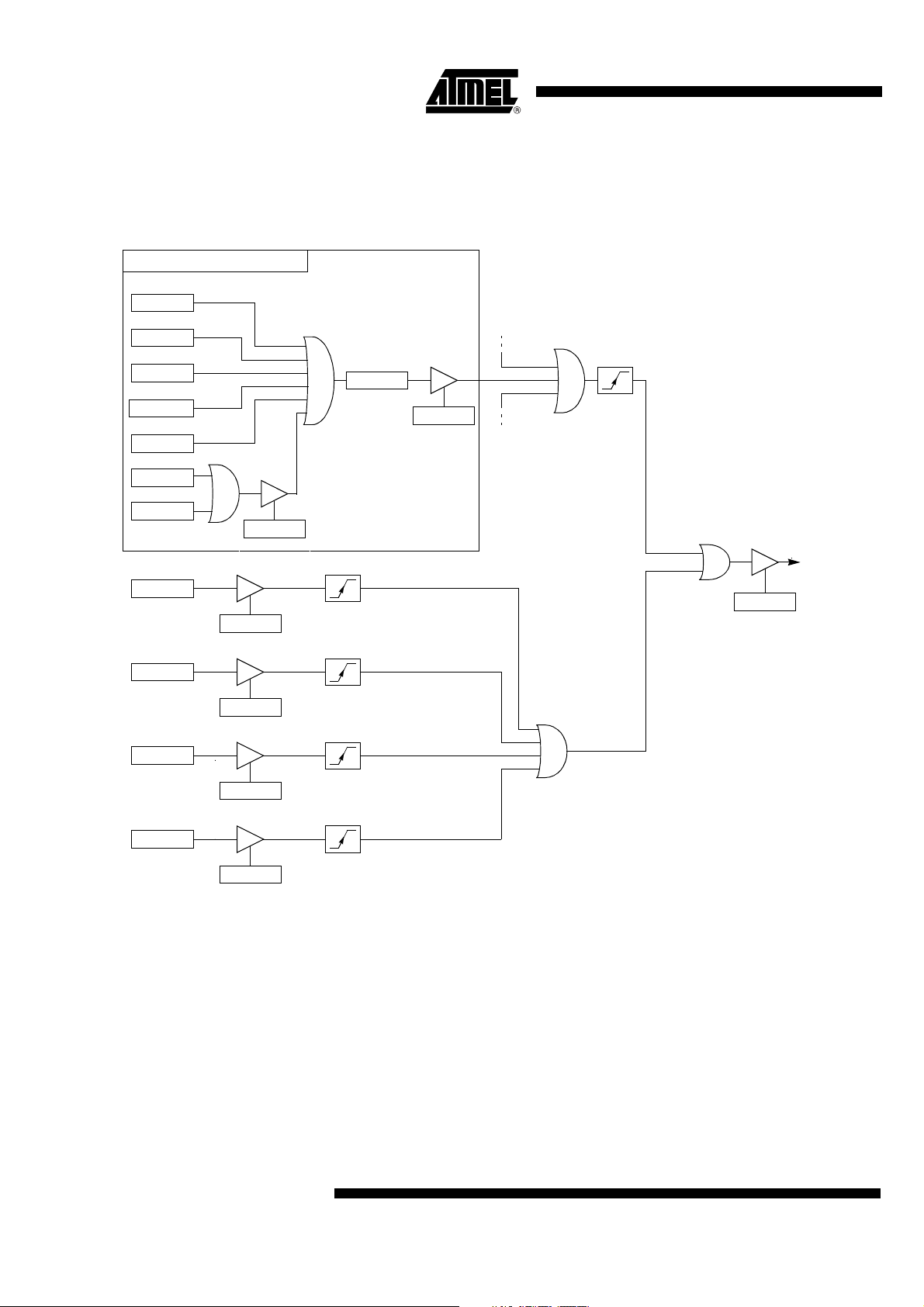
AT8xC51SND1C
Figure 72. USB Interrupt Control Block Diagram
Endpoint X (X = 0..2)
TXCMP
UEPSTAX.0
RXOUTB0
UEPSTAX.1
RXOUTB1
UEPSTAX.6
RXSETUP
UEPSTAX.2
STLCRC
UEPSTAX.3
NAKOUT
UEPCONX.5
NAKIN
UEPCONX.4
NAKIEN
UEPCONX.6
EPXINT
UEPINT.X
EPXIE
UEPIEN.X
WUPCPU
USBINT.5
EORINT
USBINT.4
SOFINT
USBINT.3
SPINT
USBINT.0
EWUPCPU
USBIEN.5
EEORINT
USBIEN.4
ESOFINT
USBIEN.3
ESPINT
USBIEN.0
EUSB
IE1.6
100
4109H–8051–01/05
 Loading...