

Page 1

查询AT83C51SND1C供应商
Features
• MPEG I/II-Layer 3 Hardwired Decoder
– Stand-alone MP3 Decoder
– 48, 44.1, 32, 24, 22.05, 16 kHz Sampling Frequency
– Separated Digital Volume Control on Left and Right Channels (Software Control
Using 31 Steps)
– Bass, Medium, and Treble Control (31 Steps)
– Bass Boost Sound Effect
– Ancillary Data Extraction
– “CRC Error” and “MPEG Frame Synchronization” Indicators
• Programmable Audio Output for Interfacing With Common Audio DAC
– PCM Format Compatible
2
–I
S Format Compatible
• 8-bit MCU C51 Core Based (F
• 2304 Bytes of Internal RAM
• 64K Bytes of Code Memory
– Flash: AT89C51SND1C, ROM: AT83C51SND1C
• 4K Bytes of Boot Flash Memory (AT89C51SND1C)
– ISP: Download from USB or UART to Any External Memor y Cards
• USB Rev 1.1 Controller
– “Full Speed” Data Transmission
• Built-in PLL
– MP3 Audio Clocks
–USBClock
• MultiMedia Card™ Interface Compatibility
• Atmel DataFlash
• IDE/ATAPI Interface
•2 Channels 10-bit ADC, 8 kHz (8-True Bit)
– Battery Voltage Monitoring
– Voice Recording Controlled by Software
• Up to 44 bits of General-purpose I/Os:
– 4-bit Interrupt Keyboard Port for a 4 x n Mat rix
– SmartMedia™ Software Interface
• Standard Two 16-bit Timers/Counters
• Hardware Watchdog Timer
• Standard Full Duplex UART with Baud Rate Generator
• Two Wire Interface (TWI) Master and Slave Modes Controller
• SPI Master and Slave Modes Controller
• Power Management
– Power-on Reset
– Software Programmable MCU Clock
– Idle Mode, Power-down Mode
• Operating Conditions:
–3V,±10%, 25 mA Typical Operating at 25°C
– Temperature Range: -40°Cto+85°C
• Packages
– TQFP80, PLCC84 (Development Board)
–Dice
®
SPI Interface Compatibility
=20MHz)
MAX
Single-Chip
Microcontroller
with M P3
Decoder and
Man-Machine
Interface
AT83C51SND1C
AT89C51SND1C
Preliminary
Summary
Description
The AT8 xC 5 1SND1C are full y integrated stand-alone hardwired MPEG I/II-L ay e r 3
decoders with a C51 microcontroller co re han dling data flow and MP3-player control.
The AT89C51SND1C includes 64K B y tes of Flash memory and al lows In-System Programming through an embedded 4K By tes of Boot Flash Memory.
Rev. 4106F–8051–10/02
Page 2

The AT83C51SND1C includes 64K Byte s of ROM memory.
The AT8xC51SND1C includes 2304 Byt es of RAM memory.
The AT8xC51SND1C provides all necessary features for man m achine interface like
timers, keyboard port, serial or parallel interf ace (USB, TWI, SPI, IDE), ADC input, I
output, and all external memory interface (NA ND or NOR Flash, SmartMedia, MultiMedia, DataFlash cards).
Typical Applications • MP3 Player
• PDA, C amera, Mobile Phone MP3
• Car Audio/Multimedia MP3
• Home Audio/Multimedia MP3
2
S
2
AT8xC51SND1C
4106F–8051–10/02
Page 3
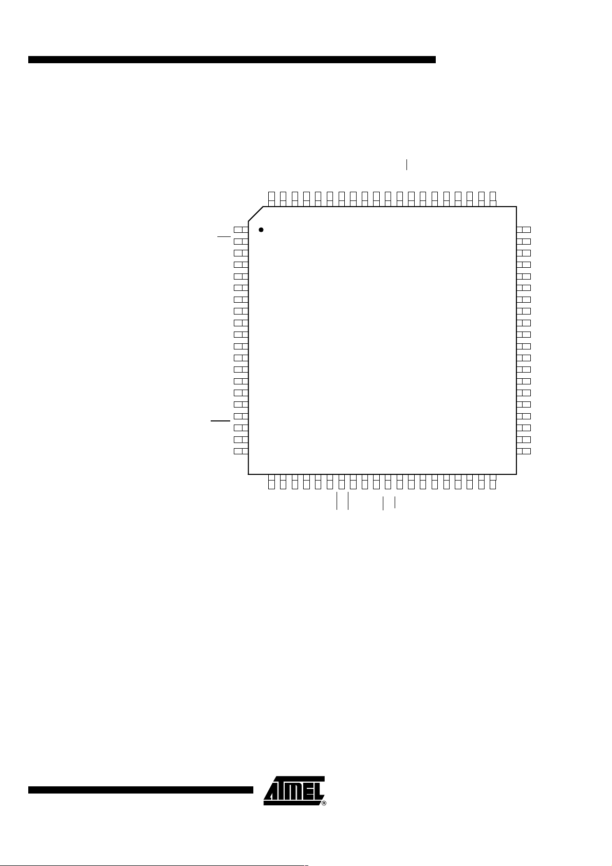
Pin Descriptions
AT8xC51SND1C
Figure 1. AT8xC51SND1C, 80-pin TQF P P ac ka ge
ALE
ISP
P1.0/KIN0
P1.1/KIN1
P1.2/KIN2
P1.3/KIN3
P1.4
P1.5
P1.6/SCL
P1.7/SDA
V
DD
P
V
DD
FILT
PVSS
VSS
X2
X1
TST
UV
DD
UVSS
P0.0/AD0
P5.0
P5.1
78
79
80
1
2
3
4
5
6
7
8
9
10
11
12
13
14
15
16
17
18
19
20
21222324252627
P0.1/AD1
77
P0.2/AD2
76
P0.3/AD3
75
P0.4/AD4
74
P0.5/AD5
73
VSS
V
717069
72
DD
P0.6/AD6
P0.7/AD7
P4.3/SS
68
AT89C51SND1C-RO (Flash)
AT83C51SND1C-RO (ROM)
28
302932
31
33
P2.0/A8
P4.0/MISO
65
64
P2.1/A9
63
P4.7
62
P4.6
61
P4.2/SCK
P4.1/MOSI
66
67
34353637383940
60
59
58
57
56
55
54
53
52
51
50
49
48
47
46
45
44
43
42
41
P4.5
P4.4
P2.2/A10
P2.3/A11
P2.4/A12
P2.5/A13
P2.6/A14
P2.7/A15
VSS
V
DD
MCLK
MDAT
MCMD
RST
SCLK
DSEL
DCLK
DOUT
VSS
V
DD
4106F–8051–10/02
D+
D-
DD
VSS
V
INT0
INT1
P3.4/T0
P3.1/TXD
P3.0/R XD
P3.2/
P3.5/T1
P3.3/
DD
V
AVSS
A
P3.7/RD
P3.6/WR
AIN0
AREFP
AREFN
P5.3
P5.2
AIN1
3
Page 4

Figure 2. AT8xC51SND1C 84-pin PLCC Package
(1)
ALE
ISP
P1.0/KIN0
P1.1/KIN1
P1.2/KIN2
P1.3/KIN3
P1.4
P1.5
P1.6/SCL
P1.7/SDA
V
DD
PA
V
DD
FILT
PAVSS
VSS
X2
NC
X1
TST
U
V
DD
UVSS
NC
11
12
13
14
15
16
17
18
19
20
21
22
23
24
25
26
27
28
29
30
31
32
3334353637
P5.1
10
P0.0/AD0
P5.0
8
9
P0.3/AD3
P0.4/AD4
P0.5/AD5
VSS
P0.2/AD2
P0.1/AD1
5
6
7
432
V
1
AT89C51SND1C-SR (Flash)
3839404142
43
DD
P0.6/AD6
P0.7/AD7
P4.3/SS
P4.2/SCK
84838281807978
444546474849505152
P2.0/A8
P4.1/MOSI
P4.0/MISO
P2.1/A9
77
P4.7
76
P4.6
75
53
NC
74
73
P4.5
7271P4.4
P2.2/A10
70
P2.3/A11
P2.4/A12
69
68
P2.5/A13
67
P2.6/A14
66
P2.7/A15
65
VSS
64
V
DD
63
MCLK
62
MDAT
61
MCMD
60
RST
59
SCLK
58
DSEL
57
DCLK
56
DOUT
55
VSS
54
V
DD
D+
D-
DD
VSS
V
P3.4/T0
P3.5/T1
P3.3/IN T 1
P3.2/IN T 0
P3.1/TXD
P3.0/RXD
DD
V
AVSS
A
P3.7/RD
P3.6/WR
AREFP
AIN1
AIN0
AREFN
NC
P5.3
P5.2
Note: 1. Only samples for development board.
Pin Descriptions All AT8xC51SND1C signals are detailed by funct ionality in Table 1 through Table 14.
Table 1. P ort s Signal Des cription
Signal
Name Type Description
Port 0
P0 isan8-bit open-drainbi-directionalI/O port. Port0 pins thathave 1s
P0.7:0 I/O
P1.7:0 I/O
writtento them float andcan be usedas high impedanceinputs. To
avoid any parasitic current consumption, floating P0 inputs must be
polarized to
Port 1
P1 is an 8-bit bi-directionalI/O portwith internal pull-ups.
V
or VSS.
DD
Alternate
Function
AD7:0
KIN3:0
SCL
SDA
4
AT8xC51SND1C
4106F–8051–10/02
Page 5

Table 1. P ort s Signal Des cription (Continue d)
Signal
Name Type Description
AT8xC51SND1C
Alternate
Function
P2.7:0 I/O
P3.7:0 I/O
P4.7:0 I/O
P5.3:0 I/O
Port 2
P2 is an 8-bit bi-directionalI/O portwith internal pull-ups.
Port 3
P3 is an 8-bit bi-directionalI/O portwith internal pull-ups.
Port 4
P4 is an 8-bit bi-directionalI/O portwith internal pull-ups.
Port 5
P5 is a 4-bit bi-directionalI/O port with internal pull-ups.
Table 2. Clock Signal Description
Signal
Name Type Description
Input to the on-chip inverting oscillator amplifier
X1 I
To usethe internal oscillator, a crystal/resonator circuit is connected to
this pin. If an external oscillator is used, its output is connected to this
pin. X1is the clocksource for internal timing.
A15:8
RXD
TXD
INT0
INT1
T0
T1
WR
RD
MISO
MOSI
SCK
SS
-
Alternate
Function
-
X2 O
FILT I
Output of the on-chip inverting oscillator amplifier
To usethe internal oscillator, a crystal/resonator circuit is connected to
this pin. If an external oscillator is used, leave X2 unconnected.
PLL low pass filter input
FILT receives the RC network ofthe PLL lowpass filter.
Table 3. Timer 0 and Timer 1 Signal Description
Signal
Name Type Description
Timer 0 Gate Input
INT0
serves asexternal run control for timer0,when selected by
GATE0 bitin TCON register.
INT0
INT1
I
External Interrupt 0
INT0
input sets IE0 in the TCON register. If bit IT0 in this register is set,
bitIE0issetbyafallingedgeonINT0
by a low level on INT0
Timer 1 Gate Input
INT1
serves asexternal run control for timer1,when selected by
GATE1 bitin TCON register.
I
External Interrupt 1
INT1
input sets IE1 in the TCON register. If bit IT1 in this register is set,
bitIE1issetbyafallingedgeonINT1
by a low level on INT1
.
.
-
-
Alternate
Function
P3.2
.IfbitIT0iscleared,bitIE0isset
P3.3
.IfbitIT1iscleared,bitIE1isset
4106F–8051–10/02
5
Page 6

Table 3. Timer 0 and Timer 1 Signal Description (Continued)
Signal
Name Type Description
Alternate
Function
T0 I
T1 I
Timer 0 External Clock Input
When Timer 0 operates as a counter, a falling edge on the T0 pin
increments the count.
Timer 1 External Clock Input
When Timer 1 operates as a counter, a falling edge on the T1 pin
increments the count.
Table 4. A udio Interface Signal Description
Signal
Name Type Description
DCLK O DAC Data Bit Clock -
DOUT O DACAudio Data -
DSEL O
SCLK O
DAC Channel Select Signal
DSEL is the sample rate clock output.
DAC System Clock
SCLK is the oversampling clock synchronized to the digital audio data
(DOUT) and the channel selection signal (DSEL).
Table 5. USB Controller Signal Description
Signal
Name Type Description
P3.4
P3.5
Alternate
Function
-
-
Alternate
Function
USB Positive Data Upstream Port
V
D+ I/O
D- I/O USB Negative Data Upstream Port -
This pin requires an external 1.5 kΩ pull-up to
operation.
for full speed
DD
Table 6. MutiMediaCard Interface Signal Description
Signal
Name Type Description
MCLK O
MCMD I/O
MDAT I/O
MMC Clock output
Data orcommandclock transfer.
MMC Command line
bi-directional command channel used for card initialization and data
transfer commands. To avoid any parasiticcurrentconsumption,
unusedMCMD input must be polarized to
MMC Data line
bi-directional data channel. To avoid any parasitic current consumption,
unused MDAT input must be polarized to
V
or VSS.
DD
V
or VSS.
DD
-
Alternate
Function
-
-
-
6
AT8xC51SND1C
4106F–8051–10/02
Page 7

Table 7. UART S ignal Desc ription
Signal
Name Type Description
Receive SerialData
RXD I/O
TXD O
RXD sends and receives data in serial I/O mode 0 and receives data in
serial I/O modes 1, 2 and 3.
TransmitSerialData
TXD outputs theshift clock in serial I/Omode 0 and transmits datain
serial I/O modes 1, 2 and 3.
Table 8. S P I Controller Sign al Description
Signal
Name Type Description
SPI Master Input Slave Output Data Line
MISO I/O
MOSI I/O
When in master mode, MISO receives data from the slave peripheral.
When inslave mode,MISO outputs datato the master controller.
SPI Master OutputSlave Input Data Line
When in master mode, MOSI outputs data to the slave peripheral.
When in slave mode, MOSI receives data from the master controller.
AT8xC51SND1C
Alternate
Function
P3.0
P3.1
Alternate
Function
P4.0
P4.1
SCK I/O
SS
SPI Clock Line
Whenin mastermode, SCKoutputsclockto theslaveperipheral.When
in slave mode, SCK receives clock from the master controller.
SPI Slave Select Line
I
When in controlled slave mode, SS
enables the slave mode.
Table 9. TWI Controller Signal Description
Signal
Name Type Description
TWISerialClock
SCL I/O
SDA I/O
When TWIcontrollerisin master mode, SCL outputsthe serial clock to
the slaveperipherals. When TWIcontroller isin slavemode, SCL
receives clockfrom the master controller.
TWISerialData
SDA is the bi-directional TWI data line.
Table 10. A/D Converter Signal Description
Signal
Name Type Description
AIN1:0 I A/D Converter Analog Inputs -
AREFP I Analog Positive Voltage ReferenceInput -
P4.2
P4.3
Alternate
Function
P1.6
P1.7
Alternate
Function
4106F–8051–10/02
AREFN I
Analog Negative Voltage Reference Input
This pinis internallyconnected to AV SS.
-
7
Page 8

Table 11. Keypad Interface Signal Description
Signal
Name Type Description
Alternate
Function
KIN3:0 I
Keypad InputLines
Holding oneofthese pinshigh orlow for 24 oscillator periods triggers a
keypad interrupt.
Table 12. External Access Signal Description
Signal
Name Type Description
A15:8 I/O
AD7:0 I/O
ALE O
ISP
RD
WR
Address Lines
Upper address lines for the external bus.
Multiplexedhigher addressand datalinesfor the IDEinterface.
Address/Data Lines
Multiplexedlower addressand datalines forthe external memoryor the
IDE interface.
AddressLatch Enable Output
ALE signals the start of an external bus cycle and indicates that valid
address information is available on lines A7:0. An external latch is used
to demultiplex the address from address/data bus.
ISP Enable Input
I/O
This signal mustbe heldtoGND through a pull-down resistoratthe
falling reset to force execution of the internal bootloader.
Read Signal
O
Read signal asserted during external data memory read operation.
Write Signal
O
Write signal asserted during external data memory write operation.
P1.3:0
Alternate
Function
P2.7:0
P0.7:0
-
-
P3.7
P3.6
Table 13. System Signal Description
Signal
Name Type Description
Reset Input
Holding thispin highfor 64 oscillator periods while the oscillator is
running resetsthe device. The Port pins are drivento theirreset
conditions when a voltage lowerthan V
RST I
TST I
oscillator is running.
Thispin has aninternalpull-downresistor which allows the device tobe
resetbyconnecting a capacitor between thispin and
AssertingRSTwhenthechipisinIdlemodeorPower-downmode
returns the chip to normal operation.
Test Input
T est mode entry signal. This pin must be set to
is applied,whetheror not the
IL
V
.
DD
V
.
DD
Alternate
Function
-
-
8
AT8xC51SND1C
4106F–8051–10/02
Page 9

Table 14. Power S ignal Des cri ption
Signal
Name Type Description
AT8xC51SND1C
Alternate
Function
V
DD
VSS GND
A
V
AVSS GND
P
V
PVSS GND
U
V
UVSS GND
DD
DD
DD
PWR
PWR
PWR
PWR
Digital SupplyVoltage
Connectt hese pins to+3Vsupplyvoltage.
Circuit Ground
Connectthese pins to ground.
Analog Supply Voltage
Connectthis pin to +3V supply voltage.
Analog Ground
Connectthis pin to ground.
PLL Supply voltage
Connectthis pin to +3V supply voltage.
PLL Circuit Ground
Connectthis pin to ground.
USB Supply Voltage
Connectthis pin to +3V supply voltage.
USB Ground
Connectthis pin to ground.
-
-
-
-
-
-
-
-
4106F–8051–10/02
9
Page 10

Internal P in Structure
Table 15. Detailed Internal Pin Structure
Circuit
V
DD
(1)
Type Pins
Watchdog Output
Latch Output
2osc
periods
TST
R
V
DD
P
VSS
VDDV
P
1
N
VSS
V
P
N
Input
Input/Output RST
RST
R
V
DD
DD
P
P
DD
3
2
Input/Output
Input/Output
TST
(2)
P1
(3)
P2
P3
P4
P53:0
P0
MCMD
MDAT
ISP
VSS
V
P
N
VSS
DD
D+
D-
Output
Input/Output
ALE
SCLK
DCLK
DOUT
DSEL
MCLK
D+
D-
Notes: 1. For information on resistors value, input/output levels, and drive capability, refer t o the Section “DC Characteristics”,
page 24.
2. When the TWI controller is enabled, P
3. In Port 2, P
transistor is continuously driven when outputting a high level bit address (A15:8).
1
,andP3transistorsare disabled allowing pseudo open-drain structure.
1,P2
10
AT8xC51SND1C
4106F–8051–10/02
Page 11

Block Diagram
Figure 3. AT8xC51S ND1C Block Diagram
INT0 INT1 MOSIMISO
3
3
DD
VSSV
DD
UVSSUV
DD
AT8xC51SND1C
SCK
AVSSAV
AREF
AIN1:0
RXDTXD
33 33444411
T1T0
SS
SCL SDA
Interrupt
Handler Unit
RAM
2304 Bytes
C51 (X2 C ORE)
MP3 Decoder
Clock and PLL
Unit
FILT X2X1
RST
ISP
Note: 1 Alternate functionof Port 1
3 Alternatefunctionof Port3
4 Alternate function of Port4
Unit
ALE
Flash
ROM
64K Bytes
Flash Boot
4K Bytes
AudioInterface
10-bit A-to-D
Converter
or
10-bitADC
8-BIT INTERNAL BUS
I2S/PCM
DSELDCLK SCLKDOUT
UART
and
BRG
USB
Controller
D+ D-
Timers 0/1
Watchdog
Interface
MCLK
MMC
MDAT
SPI/DataFlash
Controller
Keyboard
Interface
MCMD
KIN3:0
TWI
Controller
I/O
Ports
IDE
Interface
1
P0-P5
4106F–8051–10/02
11
Page 12

Application Information
Figure 4. AT8xC51S ND1C Typical Application with On-board Atmel DataFlash and TWI LCD
LCD
Battery
Ref.
DD
DD
P1.0/KIN0
P1.1/KIN1
P1.2/KIN2
P1.3/KIN3
P0.0
P0.1
P0.2
P0.3
X1
X2
FILT
P1.6/SCL
P1.7/SDA
AT8xC51SND1C
AIN1
AIN0
VREFP
V
VREFN
RST
AV
MCLK
MDAT
MCMD
UV
DD
D+
D-
USB PORT
UVSS
MMC1
MMC2
PVSS
P4.2/SCK
P4n
DataFlash
Memories
P4.0/SI
P4.1/SO
DOUT
DCLK
DSEL
SCLK
P1.4
P1.5
VSS
AVSS
Audio DAC
Figure 5. AT8xC51S ND1C Typical Application with On-board Atmel DataFlash and LCD
LCD
Battery
Ref.
DD
P1.3
P0.4
P1.0/KIN0
P1.1/KIN1
P1.2/KIN2
P0.0
P0.1
P0.2
P0.3
X1
X2
FILT
P0.5
P0.6
P0.7
P1.6/SCL
P1.7/SDA
AIN1
AIN0
VREFP
VREFN
AT8xC51SND1C
DD
V
RST
AV
MCLK
MDAT
MCMD
UV
DD
D+
D-
UVSS
USB PORT
MMC1
MMC2
12
PVSS
AT8xC51SND1C
P4.2/SCK
P4.n
DataFlash
Memories
DOUT
DCLK
DSEL
SCLK
P1.4
P4.0/SI
P4.1/SO
P1.5
VSS
AVSS
Audio DAC
4106F–8051–10/02
Page 13

Figure 6. AT8xC51S ND1C Typical Application with On-board SSFDC Flash
LCD
Battery
Ref.
P4.2
P4.4
P4.5
P4.6
P1.0/KIN0
P1.1/KIN1
P1.2/KIN2
P1.3/KIN3
P0.0
P0.1
P0.2
P0.3
X1
X2
FILT
P4.0
P4.1
P4.7
AIN1
AT8xC51SND1C
AIN0
VREFP
V
VREFN
DD
AT8xC51SND1C
DD
RST
AV
MCLK
MDAT
MCMD
UV
DD
D+
D-
UVSS
USB PORT
MMC1
MMC2
PVSS
P2
SSFDC Memories
or SmartMedia Cards
P3.6/WR
P0
P3.7/RD
SmartMedia
DOUT
DCLK
DSEL
SCLK
Figure 7. AT8xC51S ND1C Typical Application with IDE CD-RO M Drive
LCD
Battery
Ref.
P4.2
P4.4
P4.5
P4.6
P4.0
P1.0/KIN0
P1.1/KIN1
P1.2/KIN2
P0.0
P0.1
P0.2
P0.3
X1
X2
FILT
P4.1
P4.7
P1.6/SCL
P1.7/SDA
AIN1
AIN0
VREFP
AT8xC51SND1C
P3.4
P3.5
Audio DAC
V
VREFN
DD
VSS
AVSS
DD
RST
AV
MCLK
MDAT
MCMD
UV
DD
D+
D-
UVSS
USB PORT
MMC1
MMC2
4106F–8051–10/02
PVSS
P2
P0
IDE CD-ROM
P3.6/WR
P3.7/RD
DOUT
DCLK
DSEL
SCLK
P3.4
P3.5
VSS
AVSS
Audio DAC
13
Page 14

Address Sp aces The AT8xC51SND1C derivatives implement four different address spaces:
• Program/Code Memory
• Boot Memory
• Data Memory
• Special Function Registers (SFRs)
Code Memory The AT89C51SND1C and AT83C51SND1C implement 64K Bytes of on-chip pro-
gram/code memory. The AT83C51SND1 C product provides the internal p rogram/code
memory in ROM technology while the AT89C51SND1C product provides i t in Flash
technology.
The Flash memory increases ROM functionality by enabling in-circuit ele ctrical erasure
and programming. Thanks to the internal charge pump, the high voltage needed for programming or erasing Flash cells is generated on-chip using the standard V
Thus, the AT89C51SND1C can be programmed using only one voltage and allows in
application software programming commonly known as IAP. Hardware programming
mode is also available using specific programm ing tools.
Boot Memory The AT89C51SND1C implements 4K Bytes of on-chip boot me mory prov ided in Flash
technology. This bo ot memory is delivered p ro grammed with a standard bootloader software allowing In-system Programming comm only known as ISP. It also contains some
Application Programming Int erf aces routines commonly known as API allowing user to
develop his own bootloader.
voltage.
DD
Data Memory The AT8xC51SND1 derivatives implement 2304 B ytes of on-chip data R AM. T his mem-
ory is divided in two s eparate areas:
• 256 Bytes of on-chip RAM memory (standard C51 memory).
• 2048 Bytes of on-chip expanded RAM memory (E RAM accessible via MOVX
instructions).
14
AT8xC51SND1C
4106F–8051–10/02
Page 15

AT8xC51SND1C
Special Function
Registers
The Special Function Registers (SFRs) of the AT8xC51SND1 derivatives fall into the
categories detailed in Table 16 through Table 32. The relative addres ses of these S FRs
are provided together with their reset values in Table 33. In this table, the bit-addressable registers are identified by Note 1.
Table 16. C51CoreSFRs
MnemonicAddName 765 43210
ACC E0h Accumulator – – – – – – – –
BF0hBRegister ––––––––
PSW D0h
SP 81h Stack Pointer – – – – – – – –
DPL 82h
DPH 83h
ProgramStatus
Word
Data PointerLow
byte
Data PointerHigh
byte
CY AC F0 RS1 RS0 OV F1 P
––––––––
––––––––
Table 17. System Managem ent SFRs
MnemonicAddName 765 43210
PCON 87h Power Control SMOD1 SMOD0 – – GF1 GF0 PD IDL
AUXR 8Eh Auxiliary Register 0 – EXT16 M0 DPHDIS XRS1 XRS0 EXTRAM AO
AUXR1 A2h Auxiliary Register 1 – – ENBOOT – GF3 0 – DPS
NVERS FBh Version Number NV7 NV6 NV5 NV4 NV3 NV2 NV1 NV0
Table 18. PLL and System Clock SFRs
MnemonicAddName 765 43210
CKCON 8Fh Clock Control – – – – – – – X2
PLLCON E9h PLL Control R1 R0 – – PLLRES – PLLEN PLOCK
PLLNDIV EEh PLL N Divider – N6 N5 N4 N3 N2 N1 N0
PLLRDIVEFhPLLRDivider R9R8R7R6R5R4R3R2
4106F–8051–10/02
15
Page 16

Table 19. Interrupt SFRs
MnemonicAddName 765 43210
IEN0 A8h
IEN1 B1h
IPH0 B7h
IPL0 B8h
IPH1 B3h
IPL1 B2h
Interrupt Enable
Control 0
Interrupt Enable
Control 1
Interrupt Priority
Control High 0
Interrupt Priority
Control Low 0
Interrupt Priority
Control High 1
Interrupt Priority
Control Low 1
EA EAUD EMP3 ES ET1 EX1 ET0 EX0
– EUSB – EKB EADC ESPI EI2C EMMC
– IPHAUD IPHMP3 IPHS IPHT1 IPHX1 IPHT0 IPHX0
– IPLAUD IPLMP3 IPLS IPLT1 IPLX1 IPLT0 IPLX0
– IPHUSB – IPHKB IPHADC IPHSPI IPHI2C IPHMMC
– IPLUSB – IPLKB IPLADC IPLSPI IPLI2C IPLMMC
Table 20. Port SFRs
MnemonicAddName 765 43210
P0 80h 8-bit Port 0 – – – – – – – –
P1 90h 8-bit Port 1 – – – – – – – –
P2 A0h 8-bit Port 2 – – – – – – – –
P3 B0h 8-bit Port 3 – – – – – – – –
P4 C0h 8-bit Port 4 – – – – – – – –
P5 D8h 4-bit Port 5 – – – – – – – –
Table 21. Flash Memory SFR
MnemonicAddName 765 43210
FCON D1h Flash Control FPL3 FPL2 FPL1 FPL0 FPS FMOD1 FMOD0 FBUSY
Table 22. Timer SFRs
MnemonicAddName 765 43210
TCON 88h
TMOD 89h
TL0 8Ah
TH0 8Ch
TL1 8Bh
Timer/Counter 0 and
1Control
Timer/Counter 0 and
1 Modes
Timer/Counter0Low
Byte
Timer/Counter 0
High Byte
Timer/Counter1Low
Byte
TF1 TR1 TF0 TR0 IE1 IT1 IE0 IT0
GATE1 C/T1# M1 1 M01 GATE0 C/T0# M10 M00
––––––––
––––––––
––––––––
16
AT8xC51SND1C
4106F–8051–10/02
Page 17

AT8xC51SND1C
Table 22. Timer SFRs (Continued)
MnemonicAddName 765 43210
TH1 8Dh
WDTRST A6h
WDTPRG A7h
Timer/Counter 1
High Byte
WatchDog Timer
Reset
WatchDog Timer
Program
––––––––
––––––––
– – – – – WTO2 WTO1 WTO0
Table 23. MP3 Decoder SFRs
MnemonicAddName 765 43210
MP3CON AAh MP3 Control MPEN MPBBST CRCEN MSKANC MSKREQ MSKLAY MSKSYN MSKCRC
MP3STA C8h MP3 Status MPANC MPREQ ERRLAY ERRSYN ERRCRC MPFS1 MPFS0 MPVER
MP3STA1 AFh MP3 Status1 – – – MPFREQ MPBREQ – – –
MP3DAT ACh MP3 Data MPD7 MPD6 MPD5 MPD4 MPD3 MPD2 MPD1 MPD0
MP3ANC ADh MP3 Ancillary Data AND7 AND6 AND5 AND4 AND3 AND2 AND1 AND0
MP3VOL 9Eh
MP3VOR 9Fh
MP3BAS B4h
MP3 Audio Volume
Control Left
MP3 Audio Volume
Control Right
MP3 Audio Bass
Control
– – – VOL4 VOL3 VOL2 VOL1 VOL0
– – – VOR4 VOR3 VOR2 VOR1 VOR0
– – – BAS4 BAS3 BAS2 BAS1 BAS0
MP3MED B5h
MP3TRE B6h
MP3CLK EBh MP3 Clock Divider – – – MPCD4 MPCD3 MPCD2 MPCD1 M PCD0
MP3 Audio Medium
Control
MP3 Audio Treble
Control
– – – MED4 MED3 MED2 MED1 MED0
– – – TRE4 TRE3 TRE2 TRE1 TRE0
Table 24. Audio Interface SFRs
MnemonicAddName 765 43210
AUDCON0 9Ah Audio Control 0 JUST4 JUST3 JUST2 JUST1 JUST0 POL DSIZ HLR
AUDCON1 9Bh Audio Control 1 SRC DRQEN MSREQ MUDRN – DUP1 DUP0 AUDEN
AUDSTA 9Ch Audio Status SREQ UDRN AUBUSY – – – – –
AUDDAT 9Dh Audio Data AUD7 AUD6 AUD5 AUD4 AUD3 AUD2 AUD1 AUD0
AUDCLK ECh Audio Clock Divider – – – AUCD4 AUCD3 AUCD2 AUCD1 AUCD0
4106F–8051–10/02
17
Page 18

Table 25. USB Controller SFRs
MnemonicAddName 765 43210
USBCON BCh USB Global Control USBE SUSPCLK SDRMWUP – UPRSM RMWUPE CONFG FADDEN
USBADDR C6h USB Address FEN UADD6 UADD5 UADD4 UADD3 UADD2 UADD1 UADD0
USBINT BDh USB Global Interrupt – – WUPCPU EORINT SOFINT – – SPINT
USBIEN BEh
UEPNUM C7h
UEPCONX D4h
UEPSTAX CEh
UEPRST D5h USB Endpoint Reset – – – – EP3RST EP2RST EP1RST EP0RST
UEPINT F8h
UEPIEN C2h
UEPDATX CFh
UBYCTX E2h
UFNUML BAh
UFNUMH BBh
USB Global Interrupt
Enable
USB Endpoint
Number
USB Endpoint X
Control
USB Endpoint X
Status
USB Endpoint
Interrupt
USB Endpoint
Interrupt Enable
USB Endpoint X
FIFO Data
USB Endpoint X Byte
Counter
USB Frame Number
Low
USB Frame Number
High
– – EWUPCPU EEORINT ESOFINT – – E SPINT
– – – – – – EPNUM1 EPNUM0
EPEN – – – DTGL EPDIR EPTYPE1 EPTYPE0
DIR – STALLRQ TXRDY STLCRC RXSETUP RXOUT TXCMP
– – – – EP3INT EP2INT EP1INT EP0INT
– – – – EP3INTE EP2INTE EP1INTE EP0INTE
FDAT7 FDAT6 FDAT5 FDAT4 FDAT3 FDAT2 FDAT1 FDAT0
- BYCT6 BYCT5 BYCT4 BYCT3 BYCT2 BYCT1 BYCT0
FNUM7 FNUM6 FNUM5 FNUM4 FNUM3 FNUM2 FNUM1 FNUM0
– – CRCOK CRCERR – FNUM10 FNUM9 FNUM8
USBCLK EAh USB Clock Divider – – – – – – USBCD1 USBCD0
Table 26. MMC Controller SFRs
MnemonicAddName 76 543210
MMCON0 E4h MMCControl 0 DRPTR DTPTR CRPTR CTPTR MBLOCK DFMT RFMT CRCDI S
MMCON1 E5h MMC Control 1 BLEN3 BLEN2 BLEN1 BLEN0 DATDIR DATEN RESPEN CMDEN
MMCON2 E6h MMC Co ntrol 2 MMCEN DCR CCR – – DATD1 DATD0 FLOWC
MMSTA DEh
MMINT E7h MMCInterrupt MCBI EORI EOCI EOFI F2FI F1FI F2EI F1EI
MMMSK DFh
MMCMD DDh MMC Command MC7 MC6 MC5 MC4 MC3 MC2 MC1 MC0
MMDAT DCh MMC Data MD7 MD6 MD5 MD4 MD3 MD2 MD1 MD0
MMCLK EDh MMC Clock Divider MMCD7 MMCD6 MMCD5 MMCD4 MMCD3 MMCD2 MMCD1 MMCD0
18
AT8xC51SND1C
MMC Control and
Status
MMC Interrupt
Mask
– – CB USY CRC16S DATFS CRC7S RESPFS CFLCK
MCBM EORM EOCM EOFM F2FM F1FM F2EM F1EM
4106F–8051–10/02
Page 19

AT8xC51SND1C
Table 27. IDE Interface SFR
MnemonicAddName 765 43210
DAT16H F9h
High Order Data
Byte
D15 D1 4 D13 D12 D11 D10 D9 D8
Table 28. Serial I/O Port SFRs
MnemonicAddName 76 5 43210
SCON 98h Serial Control FE/SM0 SM1 SM2 REN TB8 RB8 TI RI
SBUF 99h Serial Data Buffer – – – – – – – –
SADEN B9h Slave Address Mask – – – – – – – –
SADDR A9h SlaveAddress – – – – – – – –
BDRCON 92h Baud Rate Control – – – BRR TBCK RBCK SPD SRC
BRL 91h Baud Rate Reload – – – – – – – –
Table 29. SPI Controller SFRs
MnemonicAddName 765 43210
SPCON C3h SPI Control SPR2 SPEN SSDIS MSTR CPOL CPHA SPR1 SPR0
SPSTA C4h SPI Status SPIF WCOL – MODF – – – –
SPDAT C5h SPI Data SPD7 SPD6 SPD5 SPD4 SPD3 SPD2 SPD1 SPD0
Table 30. TWI Controller SFRs
MnemonicAddName 765 43210
SSCON 93h
SSSTA 94h
SSDAT 95h
SSADR 96h
Synchronous Serial
Control
Synchronous Serial
Status
Synchronous Serial
Data
Synchronous Serial
Address
SSCR2 SSPE SSSTA SSSTO SSI SSAA SSCR1 SSCR0
SSC4 SSC3 SSC2 SSC1 SSC0 0 0 0
SSD7 SSD6 SSD5 SSD4 SSD3 SSD2 SSD1 SSD0
SSA7 SSA6 SSA5 SSA4 SSA3 SSA2 SSA1 SSGC
Table 31. Keyboard Interface SFRs
MnemonicAddName 765 43210
KBCON A3h Keyboard Co nt rol KINL3 KINL2 KINL1 KINL0 KINM3 KINM2 KINM1 KINM0
KBSTA A4h Keyboard Status KPDE – – – KINF3 KINF2 KINF1 KINF0
4106F–8051–10/02
19
Page 20

Table 32. A/D Controller SFRs
MnemonicAddName 765 43210
ADCON F3h ADC Control – ADIDL ADEN ADEOC ADSST – – ADCS
ADCLK F2h ADC Clock Divider – – – ADCD4 ADCD3 ADCD2 ADCD1 ADCD0
ADDL F4h ADC Data Low Byte – – – – – – ADAT1 ADAT0
ADDH F5h ADC Data High Byte A DAT9 ADAT8 ADAT7 ADAT6 ADAT5 ADAT4 ADAT3 ADAT2
20
AT8xC51SND1C
4106F–8051–10/02
Page 21

Table 33. SFR Addresses and Reset Values
0/8 1/9 2/A 3/B 4/C 5/D 6/E 7/F
F8h
F0h
UEPINT
0000 0000
1
B
0000 0000
DAT16H
XXXX XXXX
ADCLK
0000 0000
NVERS
1000 0100
ADCON
0000 0000
2
ADDL
0000 0000
ADDH
0000 0000
AT8xC51SND1C
FFh
F7h
E8h
E0h
D8h
D0h
C8h
C0h
B8h
B0h
A8h
A0h
98h
90h
88h
80h
1
ACC
0000 0000
1
P5
XXXX 1111
1
PSW
0000 0000
MP3STA
0000 0001
1
P4
1111 1111
1
IPL0
X000 0000
1
P3
1111 1111
1
IEN0
0000 0000
1
P2
1111 1111
SCON
0000 0000
1
P1
1111 1111
1
TCON
0000 0000
1
P0
1111 1111
1
XXXX XXXX
PLLCON
0000 1000
3
FCON
1111 0000
SADEN
0000 0000
IEN1
0000 0000
SADDR
0000 0000
SBUF
BRL
0000 0000
TMOD
0000 0000
SP
0000 0111
4
USBCLK
0000 0000
UBYCTLX
0000 0000
UEPIEN
0000 0000
UFNUML
0000 0000
IPL1
0000 0000
MP3CON
0011 1111
AUXR1
XXXX 00X0
AUDCON0
0000 1000
BDRCON
XXX0 0000
TL0
0000 0000
DPL
0000 0000
MP3CLK
0000 0000
SPCON
0001 0100
UFNUMH
0000 0000
IPH1
0000 0000
KBCON
0000 1111
AUDCON1
10110010
SSCON
0000 0000
TL1
0000 0000
DPH
0000 0000
AUDCLK
0000 0000
MMCON0
0000 0000
MMDAT
1111 1111
UEPCONX
0000 0000
SPSTA
0000 0000
USBCON
0000 0000
MP3BAS
0000 0000
MP3DAT
0000 0000
KBSTA
0000 0000
AUDSTA
1100 0000
SSSTA
1111 1000
TH0
0000 0000
MMCLK
0000 0000
MMCON1
0000 0000
MMCMD
1111 1111
UEPRST
0000 0000
SPDAT
XXXX XXXX
USBINT
0000 0000
MP3MED
0000 0000
MP3ANC
0000 0000
AUDDAT
1111 1111
SSDAT
1111 1111
TH1
0000 0000
PLLNDIV
0000 0000
MMCON2
0000 0000
MMSTA
0000 0000
UEPSTAX
0000 0000
USBADDR
1000 0000
USBIEN
0001 0000
MP3TRE
0000 0000
WDTRST
XXXX XXXX
MP3VOL
0000 0000
SSADR
1111 1110
AUXR
X000 1101
PLLRDIV
0000 0000
MMINT
0000 0011
MMMSK
1111 1111
UEPDATX
0000 0000
UEPNUM
0000 0000
IPH0
X000 0000
MP3STA1
0100 0001
WDTPRG
XXXX X000
MP3VOR
0000 0000
CKCON
0000 000X
PCON
XXXX 0000
EFh
E7h
DFh
D7h
CFh
C7h
BFh
B7h
AFh
A7h
9Fh
97h
8Fh
5
87h
0/8 1/9 2/A 3/B 4/C 5/D 6/E 7/F
Reserved
Notes: 1. SFR registers with least significant nibble address equal to 0 or 8 are bit-addressable.
2. NVERS reset value depends on the silicon version.
3. FCON register is only available in AT89C51SND1Cproduct.
4. FCON reset value is 00h in case of reset with hardware condition.
5. CKCON reset value depends on the X2B bit (programmed or unprogrammed) in the Hardware Byte.
4106F–8051–10/02
21
Page 22

Peripherals
Clock Generator System The AT8xC51SND1C internal clocks are extracted from an on-chip PLL fed by an on-
chip oscillator. Four clocks are generated respectively for the C51 core, the MP3
decoder, the au dio interface, and t he other peripherals. The C51 and peripheral clocks
are derived from the oscillator clock. The MP3 decoder clock is generated by dividing
the PLL output clock. The audio interface sample rates are also obtained by dividing the
PLL output clock.
Ports The AT8xC51SND1C implement five 8-bit ports (P0 - P4) and one 4-bit port (P5). In
addition to performing general-purpose I/Os, some ports are capable of external data
memory operations; o thers allow for alterna te functions. All I /O Ports are bi-d irect ional.
Each Port cont ains a latch, an output driver a nd an input buffer. Port 0 and Port 2 output
drivers and input buffers facilitate external memory operations. Some Port 1, Port 3 a nd
Port 4 pins serve for both general-purpose I/Os and alternate functions.
Timers/Counters The AT8xC51SND1C implement the two general-purpose, 16-bit Timers/Counters of a
standard C51. They are identified as Timer 0, Timer 1, and can independently be configured each to operate in a variety of modes as a Timer or as an event Counter. When
operating as a Timer, a Timer/Counter runs for a program med length of time, then
issues an interrupt request. When ope rating as a Counter, a Timer/Counter counts negative transitions on an external pin. After a preset number of count s , the Counter issues
an interrupt request.
Watchdog Timer The AT8xC51SND1C implement a hardw are Watchdog Timer that automatically reset s
the chip if it is allowed to t im e out. The WDT provides a means of recovering from routines that do not complete successfully due to software or hardware malfunctions.
MP3 Decoder The AT8xC51SND1C implements a MP EG I/ II audio layer 3 decoder (MP 3 deco der).
In MPEG I (ISO 11172-3 ) three layers o f compression have been standardized suppo rting three sampling frequencies: 48, 44.1, and 32 kHz. Among these layers, layer 3
allows highest compression rate of about 12:1 while still m aintaining CD audio quality.
For example, 3 minutes of CD audio (16-bit PCM, 44.1 kHz) data , which needs about
32M bytes of storage, can be encoded into only 2.7 MBytes of MPEG I audio layer 3
data.
In MPEG II (ISO 13818-3), three additional sampl ing frequencies: 24, 22.05, and 16 kHz
are supported for low bit rates applications.
The AT8xC51SND1C ca n decode in real-time the MPEG I audio layer 3 encoded data
into a PCM audio data, and also supports MPEG II audio layer 3 addition al frequencies.
Additional features are supported by the AT8xC51SND1C MP3 decoder such as volume, bass, medium, and treble co ntrols, bas s boost effect and ancillary data extraction.
Audio Output Interface T he AT8xC51SND1C implements an audi o output interface allowing the decoded audio
bitstream to be output in various formats. It is compatible with right and left justification
PCM and I
allows connection of almost all of the commercial audio DAC families a vailable on the
market.
2
S formats and the on-chip P LL (see Section “Clock Gene rator System”)
22
AT8xC51SND1C
4106F–8051–10/02
Page 23

AT8xC51SND1C
Universal Serial Bus
Interface
MultiMedia Card
Interface
IDE/ATAPI Interface The AT8xC51SND1C provide an IDE/ATAPI interface allowing connection of devices
The AT8xC51SND1C implement a full-speed USB Interface. It can be used for t he following purposes:
• Download of MP3 encoded au dio files by support ing the USB mas s storage class.
• In-System Programming by supporting the USB firmware upgrade class.
The AT8xC51SND1C implement a MultiMedia Card (MMC) interface compliant to the
V2.2 specification in MultiMedia Card mode. The MMC allows storage of MP3 encoded
audio files in removable Flash memory cards that can be easily plugged to, or removed
from the application. It can also be used for In-System Programm ing.
such as CD-ROM reader, CompactFlash
16-bit bi-directional bus part of the low-level ANSI ATA/ATAPI specification. It is provided for mass storage interfaces but could be us ed for In-System Programming using
CD-ROM.
™
cards, Hard Disk Drive, etc. It consi sts of a
Serial I/O Interface The AT8xC51SND1C implement a serial port with its own baud rate generator providing
one single synchronous communication mode and three full-duplex Universal Asynchronous Receiver Transmitter (UART) communication modes. It is provided for the
following purposes:
• In-System Programming.
• Remote control of the AT8xC51SND1C by a host .
Serial Peripheral
Interface
The AT8xC51SND1C implement a Serial P eripheral Interface (SP I) supporting m as t er
and slave modes. It is provided for the following purposes:
• Interfacing DataFlash memory and DataFlash cards for MP3 encoded audio files
storage
• Remote control of the AT8xC51SND1C by a host
• In-System Programming
TWI Controller The AT8xC51SND1C implement s a T WI controller supporting the four standard master
and slave modes with multim aster capability. It is provided for the following pur poses:
• Connection of slave devices like LCD controller, audio DAC…
• Remote control of the AT8xC51SND1C by a host
• In-System Programming
A/D Controller The AT 8x C51SND1C implements a 2-channel 10-bit (8 true bits) analog-to-digital con-
verter (ADC). It is provided for the following purposes:
• Battery monitoring
• Voice recording
• Corded remote control
Keyboard Interface The A T8x C51 SND1C implement a keyboard interface al lowing connection of 4 x n
matrix key board. It is based on 4 inputs w ith programmable interrupt capability on both
high or l ow level. These inputs are available as an alternate function of P1.3:0 and allow
exit from idle and power-down modes.
4106F–8051–10/02
23
Page 24

Electrical Characteristics
Absolute Maximum Rating
Storage Temperature......................................... -65 to +150°C
Voltage on any other Pin to V
I
per I/O Pin................................................................. 5 mA
OL
SS ......................................
Power Dissipation............................................................. 1 W
Ambient Temperature Under Bias........................ -40 to +85°C
-0.3to+4.0V
NOTE: Stressingthe device beyond the “Absolute Maxi-
mum Ratings” may cause permanent damage.
These are stress ratings only. Operation beyond
the “operating conditions” is not recommended
and extended exposure beyond the “Operating
Conditions” may affect device reliability.
V
DD ...........................................................................................
2.7 t o 3.3V
DC Characteristics
Digital Logic
Table 34. Digital D C Characteristics VDD= 2.7 to 3.3V , TA=-40° to +85°C
Symbol Parameter Min Typ
V
V
V
V
V
V
V
Input LowVoltage -0.5 0.2·VDD-0.1 V
IL
Input HighVoltage(except RST) 0.2·VDD+0.9 V
IH1
Input High Voltage(RST) 0.7·V
IH2
Output Low Voltage
(exceptP0,ALE, MCMD, MDAT, MCLK,
OL1
SCLK, DCLK, DSEL, DOUT)
Output Low Voltage
(P0, ALE, MCMD,MDAT, MCLK, SCLK,
OL2
DCLK, DSEL, DOUT)
OutputHigh Voltage
OH1
(P1, P2,P3, P4 andP5)
OutputHigh Voltage
(P0, P2 address mode, ALE, MCMD,
OH2
MDAT, MCLK, SCLK, DCLK, DSEL,
DOUT, D+, D-)
DD
V
-0.7 V IOH=-30µA
DD
V
-0.7 V IOH=-3.2mA
DD
(1)
Max Units T est Conditions
DD
V
+0.5 V
DD
0.45 V I
0.45 V I
V
=1.6mA
OL
=3.2mA
OL
24
I
Logical 0 InputCurrent (P1, P2, P3,P 4
IL
and P5)
AT8xC51SND1C
-50 µAV
IN
=0.45V
4106F–8051–10/02
Page 25

Table 34. Digital D C Characteristics VDD= 2.7 to 3.3V , TA=-40° to +85°C
Symbol Parameter Min Typ
InputLeakageCurrent(P0,ALE,MCMD,
I
MDAT, MCLK, SCLK, DCLK, DSEL,
LI
DOUT)
(1)
AT8xC51SND1C
Max Units T est Conditions
10 µA0.45<V
< V
IN
DD
I
R
C
V
I
I
I
Logic1 to0Transition Current
TL
(P1, P2,P3, P4 andP5)
Pull-down Resistor 50 90 200 kΩ
RST
Pin Capacitance 10 pF TA=25°C
IO
V
RET
DD
DL
PD
Data Retention Limit 1.8 V
DD
Operating Current TBD TBD mA
Idle Mode Current TBD TBD mA
Power-down Curre nt TBD TBD µAV
-650 µAVin=2.0V
12 MHz,
16 MHz,
20 MHz,
12 MHz,
16 MHz,
20 MHz,
V
V
V
V
V
V
< VDD<3.3V
RET
DD
DD
DD
DD
DD
DD
<3.3V
<3.3V
<3.3V
<3.3V
<3.3V
<3.3V
Note: 1. Typicalvalues are obtained using VDD=3VandTA=25°C. They are not tested and there is no guarantee on these values.
Figure 8. IDD/IDLVersus X
Frequency; VDD= 2.7 to 3.3V
TAL
TBD
TBD
(mA)
DL
/I
TBD
DD
I
4106F–8051–10/02
0
max Active mode (mA)
typActivemode(mA)
max Idle mode (mA)
typIdlemode(mA)
2681041412 2016 18
Frequency at XTAL (MHz)
25
Page 26

I
DD,IDL
and IPDTest Conditions Figure 9. IDDTest Condition, Ac t ive Mode
V
DD
RST
V
DD
V
IDD
DD
V
DD
P0
Figure 10. I
Figure 11. I
(NC)
ClockSignal
Test Condition, Idle Mode
DL
VSS
(NC)
Clock Signal
VSS
Test Condition, Power-Down Mode
PD
VSS
X2
X1
VSS
VSS
All other pins are unconnected
RST
X2
X1
VSS
All other pins areunconnected
RST
V
TST
V
DD
TST
DD
P0
V
DD
IDL
V
DD
V
DD
IPD
V
DD
26
AT8xC51SND1C
(NC)
X2
X1
VSS
VSS
All other pinsare unconnected
P0
MCMD
MDA T
TST
4106F–8051–10/02
Page 27

AT8xC51SND1C
A-to-D Converter
Table 35. A-to-D Converter DC Characteristics V
Symbol Parameter Min Typ Max Units Test Conditions
A
V
DD
AI
DD
AI
PD
AnalogSupplyVoltage 2.7 3.3 V
AnalogOperating Supply Current 600 µA
AnalogStandby Current 2 µA
= 2.7 to 3.3V , TA=-40° to +85°C
DD
A
V
AIN1:0 = 0 to A
A
V
ADEN = 0 or PD = 1
DD
DD
=3.3V
=3.3V
V
DD
AV
IN
AnalogInputVoltage AV
SS
AV
DD
V
Reference Voltage
AV
REF
R
REF
C
IA
A
A
REFN
REFP
AV
SS
2.4 AV
DD
V
V
AREF Input Resistance 10 30 kΩ TA=25°C
AnalogInputcapacitance 10 pF TA=25°C
Oscillator and Crystal
Schematic Figure 12. Crystal Co nnec tion
X1
C1
Q
C2
V
SS
X2
Note: For operation with most standard crystals, no external components are needed on X1
and X2. It may be necessary to add external capacitors on X1 and X2 to ground in special cases (max 10 pF). X1 and X2 may not be used to drive other circuits.
Parameters Table 36. Oscillator and Crystal Characteristics VDD= 2.7 to 3.3V , TA=-40° to +85°C
4106F–8051–10/02
Symbol Parameter Min Typ Max Unit
C
C
C
Internal Capacitance (X1 - VSS) 10 pF
X1
Internal Capacitance (X2 - VSS) 10 pF
X2
Equivalent Load Capacitance (X1 - X2) 5 pF
L
DL Drive Level 50 µW
F Crystal Frequency 20 MHz
RS Crystal Series Resistance 40 Ω
CS Crystal ShuntCapacitance 6 pF
27
Page 28

Phase Lock Loop
Schematic Figure 13. PLL Filter Connection
PFILT
Parameters Table 37. PLL F ilter Characteristics
=2.7to3.3V,TA=-40° to +85°C
V
DD
Symbol Parameter Min Typ Max Unit
R Filter Resistor 100 Ω
C1 Filter Capacitance 1 10 nF
C2 Filter Capacitance 2 2.2 nF
In-System Programming
Schematic Figure 14. ISP Pull-down Connection
ISP
VSS
R
C1
VSS
V
SS
C2
RISP
Parameters Table 38. ISP Pul l-Down Characte ristics V
Symbol Parameter Min Typ Max Unit
R
ISP Pull-downResistor 2.2 kΩ
ISP
= 2.7 to 3.3V , TA=-40° to +85°C
DD
28
AT8xC51SND1C
4106F–8051–10/02
Page 29

AT8xC51SND1C
AC Characteristics
External 8-bit Bus Cycles
Definition of S ymbols Table 39. External 8-bit Bus Cycles Timing Symbol Definitions
Signals Conditions
AAddress HHigh
DDataIn LLow
L ALE V V alid
Q Data Out X No Longer Valid
RRD
WWR
Timings Test conditions: capacitive load on a ll pins = 50 pF.
Table 40. External 8-bit Bus Cy c le – Data Read AC Tim ings
=2.7to3.3V,TA=-40° to +85°C
V
DD
Variable Clock
Standard Mode
Symbol Parameter
T
T
T
T
T
T
T
T
T
T
T
T
T
Clock Period 50 50 ns
CLCL
ALE Pulse Width 2·T
LHLL
Address Valid to ALE Low T
AVLL
Address Hold after ALE Low T
LLAX
ALE Low to RD Low 3·T
LLRL
RD Pulse Width 6·T
RLRH
RD High to ALE High T
RHLH
Address Valid to Valid Data In 9·T
AVDV
Address Valid to RD Low 4·T
AVRL
RD Low to Valid Data 5·T
RLDV
RD Low to address Float 0 0 ns
RLAZ
Data Hold After RD High 0 0 ns
RHDX
Instruction Float after RD
RHDZ
High
-15 T
CLCL
-20 0.5·T
CLCL
-20 0.5·T
CLCL
-30 1.5·T
CLCL
-25 3·T
CLCL
-20 T
CLCL
-30 2·T
CLCL
CLCL
2·T
ZFloating
Variable Clock
X2 Mode
-15 ns
CLCL
-20 ns
CLCL
-20 ns
CLCL
-30 ns
CLCL
-25 ns
CLCL
+20 0.5·T
-65 4.5·T
CLCL
-30 2.5·T
CLCL
-25 T
CLCL
-20 0.5·T
CLCL
-30 ns
CLCL
CLCL
CLCL
CLCL
-25 ns
CLCL
UnitMin Max Min Max
+20 ns
-65 ns
-30 ns
4106F–8051–10/02
29
Page 30

Table 41. External 8-bit Bus Cyc le – Data Write AC Timings
=2.7to3.3V,TA=-40° to +85°C
V
DD
Variable Clock
Standard Mode
Symbol Parameter
T
T
T
T
T
T
T
T
T
T
Clock Period 50 50 ns
CLCL
ALE Pulse Width 2·T
LHLL
Address Valid to ALE Low T
AVLL
AddressHold after ALE
LLAX
Low
ALE Lowto WR Low 3·T
LLWL
WR Pulse Width 6·T
WLWH
WR High to ALE High T
WHLH
Address Valid to WR Low 4·T
AVWL
Data Valid toWR High 7·T
QVWH
Data Hold after WR High T
WHQX
-15 T
CLCL
-20 0.5·T
CLCL
T
-20 0.5·T
CLCL
-30 1.5·T
CLCL
-25 3·T
CLCL
-20 T
CLCL
-30 2·T
CLCL
-20 3.5·T
CLCL
-15 0.5·T
CLCL
CLCL
+20 0.5·T
CLCL
CLCL
CLCL
CLCL
CLCL
CLCL
CLCL
CLCL
CLCL
Waveforms Figure 15. External 8-bit Bus Cycle – Dat a Re ad Waveforms
ALE
T
LHLL
T
LLRL
T
RLRH
Variable Clock
X2 Mode
UnitMin Max Min Max
-15 ns
-20 ns
-20 ns
-30 ns
-25 ns
-20 0.5·T
+20 ns
CLCL
-30 ns
-20 ns
-15 ns
T
RHLH
RD
P0
P2
T
AVLL
T
T
AVRL
T
LLAX
RLAZ
T
AVDV
T
RLDV
A15:8
D7:0A7:0
Data In
T
T
RHDZ
RHDX
30
AT8xC51SND1C
4106F–8051–10/02
Page 31

AT8xC51SND1C
Figure 16. External 8-bit B us Cycle – Data W rite Wave forms
ALE
T
LHLL
T
LLWL
T
WLWH
WR
T
AVWL
T
P0
AVLL
A7:0
T
LLAX
T
QVWH
T
D7:0
Data Out
P2
A15:8
External IDE 16-bit Bus Cycles
Definition of S ymbols Table 42. External IDE 16-bit Bus Cycles Timing Symbol D efinitions
Signals Conditions
AAddress HHigh
DDataIn LLow
L ALE V V alid
Q Data Out X No Longer Valid
RRD
ZFloating
T
WHQX
WHLH
WWR
Timings Test conditions: capacitive load on a ll pins = 50 pF.
4106F–8051–10/02
31
Page 32

Table 43. External I D E 16-bi t Bus Cycle – Data Read A C Timings
= 2.7 to 3.3V, TA=-40° to +85°C
V
DD
Symbol Parameter
T
T
T
T
T
T
T
T
T
T
T
T
T
Clock Period 50 50 ns
CLCL
ALE Pulse Width 2·T
LHLL
AddressValid to ALE Low T
AVLL
AddressHold after ALELow T
LLAX
ALE Low to RD Low 3·T
LLRL
RD Pulse Width 6·T
RLRH
RD High to ALE High T
RHLH
AddressValid to ValidData In 9·T
AVDV
AddressValid to RDLow 4·T
AVRL
RD Low to Valid Data 5·T
RLDV
RD Low to Address Float 0 0 ns
RLAZ
Data Hold after RD High 0 0 ns
RHDX
Instruction Float after RD
RHDZ
High
Variable Clock
Standard Mode
-15 T
CLCL
-20 0.5·T
CLCL
-20 0.5·T
CLCL
-30 1.5·T
CLCL
-25 3·T
CLCL
-20 T
CLCL
-30 2·T
CLCL
+20 0.5·T
CLCL
-65 4.5·T
CLCL
-30 2.5·T
CLCL
2·T
-25 T
CLCL
Variable Clock
X2 Mode
-15 ns
CLCL
-20 ns
CLCL
-20 ns
CLCL
-30 ns
CLCL
-25 ns
CLCL
-20 0.5·T
CLCL
-30 ns
CLCL
+20 ns
CLCL
-65 ns
CLCL
-30 ns
CLCL
-25 ns
CLCL
UnitMin Max Min Max
Table 44. External I DE 16-bi t Bus Cycle – D ata Write AC Tim ings
=2.7to3.3V,TA=-40° to +85°C
V
DD
Symbol Parameter
T
T
T
T
T
T
T
T
T
T
ClockPeriod 50 50 ns
CLCL
ALE Pulse Width 2·T
LHLL
Address Validto ALE Low T
AVLL
Address HoldafterALE Low T
LLAX
ALE Low to WR Low 3·T
LLWL
WR Pulse Width 6·T
WLWH
WR High to ALE High T
WHLH
Address Validto WR Low 4·T
AVWL
DataValidtoWRHigh 7·T
QVWH
Data Hold after WR High T
WHQX
Variable Clock
Standard Mode
-15 T
CLCL
-20 0.5·T
CLCL
-20 0.5·T
CLCL
-30 1.5·T
CLCL
-25 3·T
CLCL
-20 T
CLCL
-30 2·T
CLCL
-20 3.5·T
CLCL
-15 0.5·T
CLCL
+20 0.5·T
CLCL
Variable Clock
-15 ns
CLCL
-20 ns
CLCL
-20 ns
CLCL
-30 ns
CLCL
-25 ns
CLCL
-20 0.5·T
CLCL
-30 ns
CLCL
-20 ns
CLCL
-15 ns
CLCL
X2 Mode
+20 ns
CLCL
UnitMin Max Min Max
32
AT8xC51SND1C
4106F–8051–10/02
Page 33

AT8xC51SND1C
Waveforms Figure 17. External IDE 16-bit Bus Cycle – Data Read Wav ef orms
ALE
T
LHLL
T
LLRL
T
RLRH
RD
T
P0
P2
T
AVLL
T
T
AVRL
T
LLAX
RLAZ
T
AVDV
RLDV
D7:0A7:0
Data In
D15:81A15:8
T
T
RHDX
Data In
Note: D15:8 is written in DAT16H SFR.
Figure 18. External IDE 16-bit B us Cycle – Data Write Waveforms
ALE
WR
T
LHLL
T
AVLL
T
T
AVWL
LLAX
T
LLWL
T
T
WLWH
QVWH
T
RHDZ
T
WHQX
RHLH
T
WHLH
P0
P2
A7:0
A15:8
Note: D15:8 is the content of DAT16H SFR.
SPI Interface
Definition of S ymbols Table 45. SPI Interface Timing Symbol Definitions
Signals Conditions
CClock HHigh
IDataIn LLow
O Data Out V Valid
D7:0
Data Out
D15:81
Data Out
X No Longer Valid
ZFloating
4106F–8051–10/02
33
Page 34

Timings Table 46. SPI Interface Master AC Tim ing
VDD=2.7to3.3V,TA=-40° to +85°C
Symbol Parameter Min Max Unit
Slave Mode
(2)
T
CHCH
T
CHCX
T
CLCX
T
SLCH,TSLCL
T
IVCL,TIVCH
T
CLIX,TCHIX
T
CLOV,TCHOV
T
CLOX,TCHOX
T
CLSH,TCHSH
T
IVCL,TIVCH
T
CLIX,TCHIX
T
SLOV
T
SHOX
T
SHSL
T
ILIH
T
IHIL
T
OLOH
T
OHOL
Clock Period 8 T
Clock High Time 3.2 T
Clock Low Time 3.2 T
OSC
OSC
OSC
SS Low to Clockedge 200 ns
Input Data Valid to Clock Edge 100 ns
Input Data Hold afterClock Edge 100 ns
Output Data Valid after Clock Edge 100 ns
Output Data Hold Time after Clock Edge 0 ns
SS High after Clock Edge 0 ns
Input Data Valid to Clock Edge 100 ns
Input Data Hold afterClock Edge 100 ns
SS Low to Output DataValid 130 ns
Output Data Hold after SS High 130 ns
SS High to SS Low Note
(1)
Input Rise Time 2 µs
Input Fall Time 2 µs
Output Rise Time 100 ns
Output Fall Time 100 ns
MasterMode
34
T
CHCH
T
CHCX
T
CLCX
T
IVCL,TIVCH
T
CLIX,TCHIX
T
CLOV,TCHOV
T
CLOX,TCHOX
T
ILIH
T
IHIL
T
OLOH
T
OHOL
Notes: 1. Value of this parameter depends on software.
AT8xC51SND1C
Clock Period 4 T
Clock High Time 1.6 T
Clock Low Time 1.6 T
Input Data Valid to Clock Edge 50 ns
Input Data Hold after Clock Edge 50 ns
Output Data Valid after Clock Edge 65 ns
Output Data Hold Time after Clock Edge 0 ns
InputDataRiseTime 2 µs
Input Data FallTime 2 µs
Output Data Rise Time 50 ns
Output Data Fall Time 50 ns
2. Test conditions:capacitive load on all pins = 100 pF
OSC
OSC
OSC
4106F–8051–10/02
Page 35

Waveforms
Figure 19. SPI Slave Waveforms (SSCPHA = 0)
(1)
SS
(input)
T
SLCH
T
SLCL
SCK
(SSCPOL = 0)
(input)
SCK
(SSCPOL = 1)
(input)
MISO
(output)
MOSI
(input)
T
T
SLOV
SLAVE MSB OUT SLAVE LSB OUTBIT 6
T
T
IVCH
T
T
IVCL
MSB IN BIT 6 LSBI N
CHCX
CHIX
CLIX
T
CHCH
T
CLCX
T
T
CLOV
CHOV
T
T
CLOX
CHOX
T
T
CLCH
CHCL
AT8xC51SND1C
T
CLSH
T
CHSH
T
SHSL
T
SHOX
1
Note: 1. Not Defined but generally the MSB of the character, which has just been received.
Figure 20. SPI Slave Waveforms (SSCPHA = 1)
(1)
SS
1
(output)
T
CHCH
SCK
(SSCPOL = 0)
(output)
T
CHCX
T
CLCX
SCK
(SSCPOL = 1)
(output)
SI
(input)
SO
(output)
T
T
IVCH
CHIX
T
IVCLTCLIX
MSB IN BIT 6 LSB IN
T
CLOV
T
CHOV
MSB OUTPort Data LSB OUT Port DataBIT 6
Note: 1. Not Defined but generally the LSB of the character, which has just been received.
T
T
CLCH
CHCL
T
T
CLOX
CHOX
4106F–8051–10/02
35
Page 36

Figure 21. SPI Master Waveforms (S S C PHA = 0)
(1)
SS
1
(input)
T
SLCH
T
SLCL
T
CHCH
SCK
(SSCPOL = 0)
(input)
T
CHCX
T
CLCX
SCK
(SSCPOL = 1)
(input)
T
SLOV
MISO
(output)
MOSI
(input)
SLAVE MSB OUT SLAVE LSB OUTBIT 6
1
T
T
IVCH
CHIX
T
T
IVCL
CLIX
MSB IN
Note: SS handled by software using general purpose port pin.
Figure 22. SPI Master Waveforms (S S C PHA = 1)
(1)
SS
1
(output)
T
CHCH
SCK
(SSCPOL = 0)
(output)
SCK
(SSCPOL = 1)
(output)
(input)
SO
(output)
T
SI
T
T
IVCH
T
IVCLTCLIX
CLCX
CHIX
CHCX
T
MSB IN BIT 6 LSB IN
T
CLOV
T
CHOV
MSB OUTPortData LSB OUT Port DataBIT 6
T
CLCH
T
CHCL
T
T
CHOV
CLOV
T
T
CHOX
CLOX
BIT 6 LSB IN
T
CLCH
T
CHCL
T
CLOX
T
CHOX
T
T
CLSH
CHSH
T
SHSL
T
SHOX
Note: SS handled by software using general purpose port pin.
36
AT8xC51SND1C
4106F–8051–10/02
Page 37

Two-wire In terface
Timings Table 47. TWI Interface AC Timing
zV
= 2.7 to 3.3V, TA=-40° to +85°C
DD
AT8xC51SND1C
INPUT
Min
Symbol Parameter
T
HD; STA Start condition holdtime 14·T
TLOW SCL Low Time 16·T
THIGH SCLHighTime 14·T
Max
CLCL
CLCL
CLCL
(4)
(4)
(4)
TRC SCLRiseTime 1µsNote
TFC SCL Fall Time 0.3 µs0.3µs
TSU;DAT1 DataSet-up Time 250 ns 20·TCLCL
TSU; DAT2 SDA Set-up Time (before repeated START condition) 250 ns 1 µs
TSU; DAT3 SDA Set-up Time (before STOP condition) 250 ns 8·T
THD; DAT Data Hold Time 0 ns 8·TCLCL
TSU; STA Repeated START Set-up Time 14·TCLCL
TSU;STO STOP condition Set-up Time 14·TCLCL
TBUF Bus Free Time 14·TCLCL
(4)
(4)
(4)
TRD SDA Rise Time 1 µsTFD SDA Fall Time 0.3 µs0.3µs
OUTPUT
Min
Max
(1)
4.0 µs
(1)
4.7 µs
(1)
4.0 µs
(2)
(3)
(4)
(1)
CLCL
(4)
-TFC
(1)
4.7 µs
(1)
4.0 µs
(1)
4.7 µs
(2)
(3)
-TRD
(4)
Notes: 1. At 100 kbit/s. At other bit-rates this value is inversely proportional to the bit-rate of
100 kbit/s.
2. Determined by the external bus-line capacitance and the external bus-line pull-up
resistor, this must be < 1 µs.
3. Spikes on the SDA and SCL lines with a duration of less than 3·
TCLCL will be filtered
out. Maximum capacitance on bus-lines SDA and SCL = 400 pF.
4.
TCLCL =T
= one oscillator clock period.
OSC
Waveforms
Figure 23. TWI Waveforms
STARTorRepeatedSTART Condition
SDA
(INPUT/OUTPUT)
SCL
(INPUT/OUTPUT)
4106F–8051–10/02
T
FD
THD;STA
Repeated START Condition
T
T
rd
STOP Condition
SU
;STA
Tsu;STO
T
DAT3
T
rc
T
fc
su;
0.7 V
0.3 V
T
T
HIGH
LOW
TSU;DAT1
THDDAT
Tsu;DAT2
STARTCondition
T
buf
DD
DD
0.7 V
0.3 V
DD
DD
37
Page 38

MMC Interface
Definition of S ymbols Table 48. MMC Interface Timing Symbol Definitions
Signals Conditions
CClock HHigh
DDataIn LLow
O Data Out V Valid
Timings Table 49. MMC Interface AC Timings
=2.7to3.3V,TA=0to70°C, CL ≤ 100 pF (10 Cards)
V
DD
Symbol Parameter Min Max Unit
X No Longer Valid
T
T
T
T
T
T
T
T
T
CHCH
CHCX
CLCX
CLCH
CHCL
DVCH
CHDX
CHOX
OVCH
Clock Period 50 n s
Clock High Time 10 ns
Clock Low Time 10 ns
Clock Rise Time 10 ns
Clock Fall Time 10 ns
Input Data Validto Clock High 3 ns
Input Data Hold after Clock High 3 ns
Output Data Hold after Clock High 5 ns
Output Data Valid to Clock High 5 ns
Waveforms Figure 24. MM C Input-Output Waveforms
T
CHCX
MCLK
T
CHIX
MCMD Input
MDAT Input
T
CHOX
MCMD Output
MDAT Output
T
CHCL
T
CHCH
T
CLCX
T
T
OVCH
CLCH
T
IVCH
38
AT8xC51SND1C
4106F–8051–10/02
Page 39

Audio I nterface
Definition of S ymbols Table 50. Audio Interface Timing Symbol Defini tions
Signals Conditions
CClock HHigh
O Data Out L Low
S Data Select V Valid
Timings Table 51. Audio Interface AC Timings
=2.7to3.3V,TA=0to70°C, CL ≤ 30pF
V
DD
Symbol Parameter Min Max Unit
T
CHCH
T
CHCX
T
CLCX
T
CLCH
T
CHCL
T
CLSV
T
CLOV
Note: 32-bit format with Fs = 48 kHz.
ClockPeriod 325.5
ClockHigh Time 30 ns
Clock Low Time 30 ns
ClockRise Time 10 ns
Clock Fall Time 10 ns
Clock Low to Select Valid 10 ns
Clock Low to Data Valid 10 ns
AT8xC51SND1C
X No Longer Valid
(1)
ns
Waveforms Figure 25. Audio Interface Waveforms
T
CHCX
DCLK
DSEL
DDAT
T
CLOV
Right Left
T
CHCL
T
CHCH
T
CLSV
T
CLCX
T
CLCH
4106F–8051–10/02
39
Page 40

Analog to Digital Converter
Definition of S ymbols Table 52. Analog to Digital Converter Timing Symbol Definitions
Signals Conditions
CClock HHigh
E Enable (ADEN bit) L Low
S
Start Conversion
(ADSST bit)
Characteristics Table 53. Analog-to-Digital Converter AC C harac t eristics
=2.7to3.3V,TA=0to70°C
V
DD
Symbol Parameter Min Max Unit
T
CLCL
T
EHSH
T
SHSL
D
LE
I
LE
O
SE
G
E
Notes: 1. AVDD=AV
code.
2. The differential non-linearity is the difference between the actual step width and the
ideal step width (see Figure 27).
3. The integral non-linearity is the peak difference between the center of the actual step
and the ideal transfer curve after appropriate adjustment of gain and offset errors
(see Figure 27).
4. The offset error is the absolute difference between the straight line, which fits the
actual transfercurve(after removing of gain error); and the straight line, which fits the
ideal transfer curve (see Figure 27).
5. The gain error is t he relative difference in percent between the straight line which fits
the actual transfer curve (after removing of offset error); and the straight line, which
fits the ideal transfer curve (see Figure 27).
Clock Period 1.43 µs
Start-up Time 4 µs
Conversion Time 11·T
Differentialnon-
linearity error
Integral non-
linearity error
Offset error
Gain error
REFP
(1)( 2)
(1)(3)
(1)(4)
(1)(5)
=3.0V,AVSS=AV
= 0 V. ADC is monotonic with no missing
REFN
CLCL
µs
TBD LSB
TBD LSB
TBD LSB
TBD %
Waveforms
Figure 26. An alog-to-Digital Converter Internal Wavef orms
CLK
T
CLCL
40
ADEN Bit
ADSST Bit
AT8xC51SND1C
T
EHSH
T
SHSL
4106F–8051–10/02
Page 41

Figure 27. An alog to Digital Converter Characteristics
Code Out
1023
1022
1021
1020
1019
1018
Ideal Transfer curve
Offset
Error
O
SE
AT8xC51SND1C
Gain
Error
G
E
7
6
5
4
3
2
1
0
0
1 2 3 4 5 6 7 1018 10191020 102110221023 1024
Offset
Error
1LSB
(ideal)
Centerof a Step
Integral non-linearity
Differential non-linearity
Example of an Actual Transfer Curve
Flash Memory
Definition of S ymbols Table 54. Flash Memory Timing Symbol Definitions
Signals Conditions
SISP
RRST VValid
B FBUSYflag X No LongerValid
AVIN (LSBideal)
LLow
Timings Table 55. Flash Memory AC Timing
V
=2.7to3.3V,TA=-40° to +85°C
DD
Symbol Parameter Min Typ Max Unit
4106F–8051–10/02
T
T
T
SVRL
RLSX
BHBL
Input ISP ValidtoRSTEdge 50 ns
Input ISP Hold after RST Edge 50 ns
Flash InternalBusy (Programming) Time 10 ms
41
Page 42

Waveforms Figure 28. Flash Memory – ISP Waveforms
RST
T
SVRL
ISP1
Note: ISP must be driven through a pull-down resistor (see Section “In-System Programming”,
page 28).
Figure 29. Flash Memory – Internal Busy Waveforms
T
RLSX
FBUSY Bit
T
BHBL
External Clock Drive and Logic Level R eferences
Definition of S ymbols Table 56. External Clock Timing Symbol Definitions
Signals Conditions
CClock HHigh
Timings Table 57. External Clock AC Timings
=2.7to3.3V,TA=0to70°C
V
DD
Symbol Parameter Min Max Unit
T
T
T
T
T
CLCL
CHCX
CLCX
CLCH
CHCL
T
CR
Clock Period 50 n s
High Time 10 ns
Low Time 10 ns
Rise Time 3 ns
FallTime 3 ns
CyclicRatioinX2mode 40 60 %
LLow
X No Longer Valid
Waveforms Figure 30. External Clock W av eform
V
-0.5
42
DD
0.45 V
AT8xC51SND1C
V
IH1
V
IL
T
CHCL
T
CLCX
T
CLCH
T
CLCL
T
CHCX
4106F–8051–10/02
Page 43

Figure 31. AC T es ting Input/O utput Wavef orms
INPUTS OUTPUTS
-0.5
DD
0.45 V
0.7
0.3 V
V
DD
DD
VIHmin
V
max
IL
Notes: 1. During AC testing, all inputs are driven at VDD-0.5V for a logic 1 and 0.45V for a logic 0.
2. Timing measurements are made on all outputs at V
min for a logic 1 and VILmax for a logic 0.
IH
Figure 32. Flo at Wavef orms
AT8xC51SND1C
V
LOAD
V
V
LOAD
LOAD
+0.1V
-0.1V
Timing Reference Points
VOH-0.1V
V
+0.1V
OL
Note: For timing purposes,a port pin is no longer floating when a 100 mV change from load voltageoccursand beginsto float when a
100 mV change from the loading V
level occurs with IOL/IOH= ±20 mA.
OH/VOL
4106F–8051–10/02
43
Page 44

Ordering Information
Table 58. Ordering Information
Supply
Part Number Memory Size
AT89C51SND1C-ROTIL 64K Flash 3V Industrial 40 MHz TQFP80 Tray
(1)
AT83SND1Axxx
Notes: 1. Refers to ROM code.
2. PLCC84 package only available for development board.
-ROTIL 64K ROM 3V Industrial 40 MHz TQFP80 Tray
Voltage
Temperature
Range Max Frequency Package
(2)
Packing
44
AT8xC51SND1C
4106F–8051–10/02
Page 45

Package Information
TQFP80
AT8xC51SND1C
4106F–8051–10/02
45
Page 46

PLCC84
46
AT8xC51SND1C
4106F–8051–10/02
Page 47

Atmel Headquarters Atmel Operations
Corporate Headquarters
2325 Orchard Parkway
San Jose, CA 951 31
TEL 1(408) 441-0311
FAX 1(408) 487-2600
Europe
Atmel Sa rl
Route des Arsenaux 41
Case Postale 8 0
CH-1705 Fri bour g
Switzerland
TEL (41) 26-426-5555
FAX (41) 26- 426- 5500
Asia
Room 121 9
Chinachem Golden Plaza
77 Mody Ro ad T simh atsui
East Kowl oon
Hong Kong
TEL (852) 2721-9778
FAX (852) 272 2-13 69
Japan
9F, Tonets u Shi nkawa B ldg.
1-24-8 Sh inkawa
Chuo-ku, Tok yo 10 4-00 33
Japan
TEL (81) 3 -3523- 3551
FAX (81) 3 -3523- 7581
Memory
2325 Orch ard P arkway
San Jose, C A 95 131
TEL 1(408 ) 441-0 311
FAX 1(408 ) 436 -4314
Microcontrollers
2325 Orch ard P arkway
San Jose, C A 95 131
TEL 1(408 ) 441-0 311
FAX 1(408 ) 436 -4314
La Chantr erie
BP 70602
44306 Na ntes C ede x 3, Fra nce
TEL (33) 2-40-18-18-18
FAX (33) 2- 40- 18-19- 60
ASIC/ASSP/Smart Cards
Zone Indus trie lle
13106 Ro usse t Cedex, France
TEL (33) 4-42-53-60-00
FAX (33) 4- 42- 53-60- 01
1150 East C hey enne Mtn. Blvd.
Colorado Springs, C O 8 090 6
TEL 1(719 ) 576-3 300
FAX 1(719 ) 540 -1759
Scottish E nterp rise Te chno logy P ark
Maxwell Building
East Kilbrid e G75 0Q R, Scot land
TEL (44) 1355-803-000
FAX (44) 13 55-24 2-74 3
RF/Automotive
Theresienstrasse 2
Postfach 3 535
74025 Heil bronn, Germany
TEL (49) 71-31-67-0
FAX (49) 71- 31- 67-2340
1150 East Cheyenne Mtn. Blvd.
Colorado Springs, CO 80906
TEL 1(719) 576-3300
FAX 1(719) 540-1759
Biometrics/Imaging/Hi-Rel MPU/
High Speed Converters/RF Datacom
Avenue de R och epleine
BP 123
38521 Saint-Eg reve Cedex, Fra nce
TEL (33) 4 -76-58 -30-0 0
FAX (33) 4 -76-5 8-34- 80
e-mail
literature@atmel.com
Web Site
http://www.atmel.com
© At mel Cor por ation 200 2.
Atmel Corpora tion makes no w a r r an t y for the use of its product s, other than those expressly c ontained in the Company’s standard warran ty
which is detailed in Atmel’s Terms and Conditions located on the Company’s web site. The Company assumes no responsibility for any errors
which may appear in this document, reserves the right to change devices or specifications detailed herein at any time without notice, and does
not make any commitment to update the information contained herein. No licenses to patents or other intellectual property of Atmel are granted
by the Com pan y in connec ti on with the sale of Atmel p r oducts, express ly or by im plication . Atmel’s products are no t author iz ed for use as c r it i c al
components in life support devices or systems.
ATMEL®and DataFlash®are registered tradema rk of Atmel. MultiMedi a Card®is a registered trademark of
MultiM ed ia Co r o poration. Sm artMedia
trademark of CompactFlash Corporation.
Other term s and pro du c t nam es ma y be the trad em a r ks of oth ers.
®
is a registered trademark of Toshiba Corporation. CompactFlash™is a
Printedonrecycledpaper.
4106F–8051–10/02 /0M
 Loading...