


查询AT83C5111供应商
Features
• 80C51 Compatible
– Three I/O Ports
– Two 16-bit Timer/Counters
– 256 Bytes RAM
• 4K Bytes ROM/OTP Program Memory with 64 Bytes Encryption Array and 3 Security
Levels
• High-Speed Architecture
– 33 MHz at 5V (66 MHz Equivalent)
– 20 MHz at 3V (40 MHz Equivalent)
– X2 Speed Improvement Capability (6 Clocks/Machine Cycle)
• 10-bit, 8 Channels A/D Converter
• Hardware Watchdog Timer
• Programmable I/O Mode: Standard C51, Input Only, Push-pull, Open Drain
• Asynchronous Port Reset
• Full Duplex Enhanced UART with Baud Rate Generator
• SPI, Master Mode
• Dual System Clock
– Crystal or Ceramic Oscillator (33/40 MHz)
– Internal RC Oscillator (12 MHz)
– Programmable Prescaler
• Programmable Counter Array with High-speed Output, Compare/Capture, Pulse Width
Modulation and Watchdog Timer Capabilities
• Interrupt Structure
– 8 Interrupt Sources
– 4 Interrupt Priority Levels
• Power Control Modes
– Idle Mode
– Power-down Mode
– Power-off Flag
• Power Supply: 2.7 - 5.5V
• Temperature Range: Industrial (-40 to 85
• Package: SO24, DIL24, SSOP24
o
C)
Low Pin Count
8-bit
Microcontroller
with A/D
Converter
AT83C5111
AT87C5111
Description
The AT8xC5111 is a high-performance ROM/OTP version of the 80C51 8-bit microcontroller in low pin count package.
The AT8xC5111 retains all the features of the standard 80C51 with 4K Bytes
ROM/OTP program memory, 256 bytes of internal RAM, an 8-source, 4-level interrupt
system, an on-chip oscillator and two timer/counters.
The AT8xC5111 is dedicated for analog interfacing applications. For this, it has a 10bit, 8 channels A/D converter and a five-channel Programmable Counter Array.
In addition, the AT8xC5111 has a Hard ware Watchdog Timer, a versatile serial chan nel that facili tates mu ltiproc ess or com munic ation (E UART) with an i ndepen dent baud
rate generator, an SPI serial bus controller an d a X2 spe ed im prov eme nt mechanism.
The X2 feature permits keeping the same CPU power at an oscillator frequency
divided by two. The prescaler allows to decrease CPU and peripherals clock
frequency.
The fully static design of the AT8xC5111 can reduce system powe r consumption b y
bringing the clock frequency down to any value, even DC, without loss of data.
The AT8xC5111 has 3 software-selectable modes of reduced activity for further reduction in power consumption. In the idle mode, the CPU is frozen while the peripherals
are still operating. In the quiet mode, only the A/D converter is operating.
Rev. 4190A–8051–11/0 2
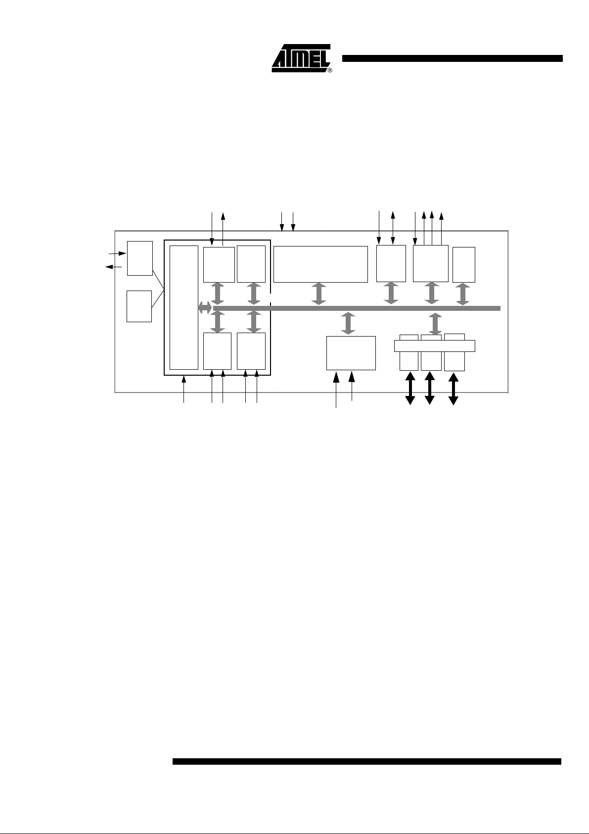
Block Diagram
(2)
XTAL1
(2)
XTAL2
Xtal
Osc
RC
Osc
In the power-down mode, the RAM is saved and all other functions are inoperative. Two
oscillator sources, crystal and RC, provide a versatile power management.
The AT8xC5111 is proposed in low-pin count packages. Port 0 and Port 2 (address/data
buses) are not available .
MISO
MOSI
SPSCK
(3)
(3)
SPI
(3)
SS
Watch
Dog
CPU
RxD
(2)(2)
EUART
BRG
TxD
C51
CORE
RAM
256
x8
IB-bus
Vss
Vcc
ROM /OTP
4K *8
(1)
ECI
(1)
PCA
CEX0-4
(3)
(2)
Notes: 1. Alternate function of Port 1.
2. Alternate function of Port 3.
3. Alternate function of Port 4.
Timer 0
Timer 1
(2) (3) (2) (3)
PP
RST/V
T0
T1
INT
Ctrl
INT0
A/D
Converter
(3)
INT1
REF
V
AIN0-7
Parallel I/O Ports
Port 3
Port 1
P1
P3
Port 4
P4
2
AT8xC5111
4190A–8051–11/02

AT8xC5111
SFR Mapping The Special Function Registers (SFRs) of the AT8xC5111 belong to the following
categories:
• C51 core registers: ACC, B, DPH, DPL, PSW, SP, AUXR1
• I/O port registers: P1, P3, P4, P1M1, P1M2, P3M1, P3M2, P4M1, P4M2
• Timer registers: TCON, TH0, TH1, TMOD, TL0, TL1
• Serial I/O port registers: SADDR, SADEN, SBUF, SCON, BRL, BDRCON
• Power and clock control registers: CKCON0, CKCON1, OSCCON, CKSEL, PCON,
CKRL
• Interrupt system registers: IE, IE1, IPL0, IPL1, IPH0, IPH1
• Watchdog Timer: WDTRST, WDTPRG
• SPI: SPCON, SPSTA, SPDAT
• PCA: CCAP0L, CCAP1L, CCAP2L, CCAP3L, CCAP4L, CCAP0H, CCAP1H,
CCAP2H, CCAP3H, CCAP4H, CCAPM0, CCAPM1, CCAPM2, CCAPM3,
CCAPM4, CL, CH, CMOD, CCON
• ADC: ADCCON, ADCCLK, ADCDATH, ADCDATL, ADCF
4190A–8051–11/02
3

Table 1. SF R Addres se s and Res et Val ues
0/8 1/9 72/A 3/B 4/C 5/D 6/E 7/F
F8h
F0h
E8h
E0h
D8h
D0h
C8h
C0h
B8h
B0h
A8h
B
0000 0000
ACC
0000 0000
CCON
00X0 0000
PSW
0000 0000
P4
1111 1111
IPL0
0000 0000
P3
1111 1111
IE0
0000 0000
CH
0000 0000
CL
0000 0000
CMOD
X000 0000
SADEN
0000 0000
IE1
0000 0000
SADDR
0000 0000
CCAP0H
XXXX XXXX
ADCLK
0000 0000
CCAP0L
XXXX XXXX
P1M2
0000 0000
CCAPM0
00XX X000
IPL1
0000 0000
CCAP1H
XXXX XXXX
ADCON
0000 0000
CCAP1L
XXXX XXXX
CCAPM1
X000 0000
SPCON
0001 0100
IPH1
0000 0000
CCAP2H
XXXX XXXX
ADDL
XXXXXX00
CCAP2L
XXXX XXXX
P3M2
0000 0000
CCAPM2
X000 0000
P1M1
0000 0000
SPSTA
XXXXXXXX
CCAP3H
XXXX XXXX
ADDH
0000 0000
CCAP3L
XXXX XXXX
P4M2
0000 0000
CCAPM3
X000 0000
P3M1
0000 0000
SPDAT
XXXX XXXX
CCAP4H
XXXX XXXX
ADCF
0000 0000
CCAP4L
XXXX XXXX
CCAPM4
X000 0000
P4M1
0000 0000
CONF
IPH0
X000 0000
CKCON1
XXXX XXX0
FFh
F7h
EFh
E7h
DFh
D7h
CFh
C7h
BFh
B7h
AFh
A0h
98h
90h
88h
80h
0000 0000
0000 0000
Reserved
AUXR1
XXXXXXX0
SCON
P1
1111 1111
TCON
0/8 1/9 2/A 3/B 4/C 5/ D 6/E 7/F
SBUF
XXXX XXXX
TMOD
0000 0000
SP
0000 0111
BRL
0000 0000
TL0
0000 0000
DPL
0000 0000
BDRCON
0000 0000
TL1
0000 0000
DPH
0000 0000
TH0
0000 0000
TH1
0000 0000
CKSEL
XXXX XXX1
WDRST
0000 0000
OSCCON
XXXX XX01
WDTPRG
0000 0000
CKRL
1111 1111
CKCON0
X000X000
PCON
00X1 0000
A7h
9Fh
97h
8Fh
87h
4
AT8xC5111
4190A–8051–11/02
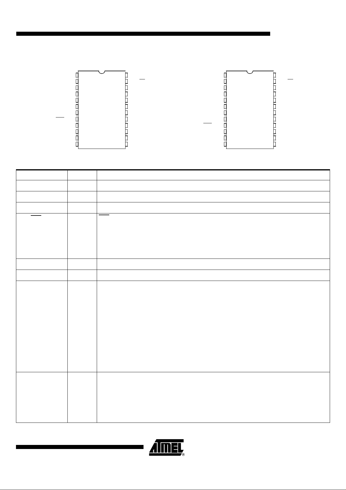
Pin Configuration
AT8xC5111
P4.4/MISO/AIN4
P4.5/MOSI/AIN5
P4.6/SPSCK/AIN6
P4.7/AIN7
RST
P1.7/CEX4
P1.6/CEX3
VREF
VSS
VCC
/VPP
XTAL2
XTAL1
1
2
3
4
5
6
7
8
9
10
11
12
SO24
DIL24
Pin Descriptions
Mnemoni c Type Name and Fun c t i on
V
SS
V
CC
VREF I VREF: A/D converter positive reference input
/VPP
RST
I Ground: 0V reference
I Power Supply: This is the power supply voltage for normal, idle and power-down operation.
RST/VPP: Reset/Programming Supply Voltage:
A low on this pin for two machine cycles while the oscillator is running, resets the device. This pin
I
has no pull-up. In order to use the internal power-on reset, an external pull-up resistor must be
connected.
This pin also rec eives the 12 V programm ing pulse w hich will start th e EPROM pro gramming and the
manufacturer test modes.
24
23
P4.2/SS/AIN2
22
P4.1/AIN1/T1
P4.0/AIN0
21
P3.0/RxD
20
P3.1/TxD
19
P1.2/ECI
18
P1.3/CEX0
17
P1.4/CEX1
16
P1.5/CEX2
15
P3.2/INT0
14
P3.3/T0
13
P4.3/INT1/AIN3
P4.4/MISO/AIN4
P4.5/MOSI/AIN5
P4.6/SPSCK/AIN6
VREF
VSS
AVSS
AVCC
VCC
RST
/VPP
XTAL2
XTAL1
P1.6/CEX3
1
2
3
4
5
SSOP24
6
7
8
9
10
11
12
24
23
P4.2/SS/AIN2
22
21
P3.0/RxD
20
19
18
17
16
15
14
13
P4.3/INT1/AIN3
P4.1/AIN1/T1
P4.0/AIN0
P3.1/TxD
P1.2/ECI
P1.3/CEX0
P1.4/CEX1
P1.5/CEX2
P3.2/INT0
P3.3/T0
XTAL1 I XTAL1 : Input to the inverting oscillator amplifier and input to the internal clock generator circuits
XTAL2 O XTAL2 : Output from the inverting oscillator amplifier
P1.2 - P1.7
I/O
Port 1: Port 1 is an 6-bit programmable I/O port . See Section “Ports”, page 18 for a description of
I/O ports.
Alternate functions for Port 1 include:
I/O ECI (P1.2): External Clock for the PCA
I/O CEX0 (P1.3): Capture/Compare External I/O for PCA module 0
I/O CEX1 (P1.4): Capture/Compare External I/O for PCA module 1
I/O CEX2 (P1.5): Capture/Compare External I/O for PCA module 2
I/O CEX3 (P1.6): Capture/Compare External I/O for PCA module 3
I/O CEX4 (P1.7): Capture/Compare External I/O for PCA module 4
P3.0 - P3.3 I/O
Port 3: Port 3 is an 6-bit programmable I/O port with internal pull-ups. See Section "Ports", page 18
for a description of I/O ports.
Port 3 also serves the special features of the 80C51 family, as listed below.
I/O RXD (P3.0): Serial input port
I/O TXD (P3.1): Serial output port
4190A–8051–11/02
5

Mnemoni c Type Name and Fun c t i on
I/O INT0 (P3.2): External interrupt 0
I/O T0 (P3.3): Timer 0 external input
P4.0 - P4.7
Port 4: Port 4 is an 8-bit programmable I/O port w i th in tern al p ull -up s . See Sec tio n "Po rt s" , p a ge18
I/O
I/O AIN0 (P4.0): A/D converter input 0
I/O
I/O
I/O
I/O
I/O
I/O
I/O AIN7 (P4.7): A/D converter input 7
for a description of I/O ports.
Port 4 is also the input port of the analog-to-digital converter.
AIN1 (P4.1): A/D converter input 1
T1: Timer 1 external input
AIN2 (P4.2): A/D converter input 2
: Slave select input of the SPI controllers
SS
AIN3 (P4.3): A/D converter input 3
: External interrupt 1
INT1
AIN4 (P4.4): A/D converter input 4
MISO: Master IN, Slave OUT of the SPI controllers
AIN5 (P4.5): A/D converter input 5
MOSI: Master OUT, Slave IN of the SPI controllers
AIN6 (P4.6): A/D converter input 6
SPSCK: Clock I/O of the SPI controll ers
6
AT8xC5111
4190A–8051–11/02

AT8xC5111
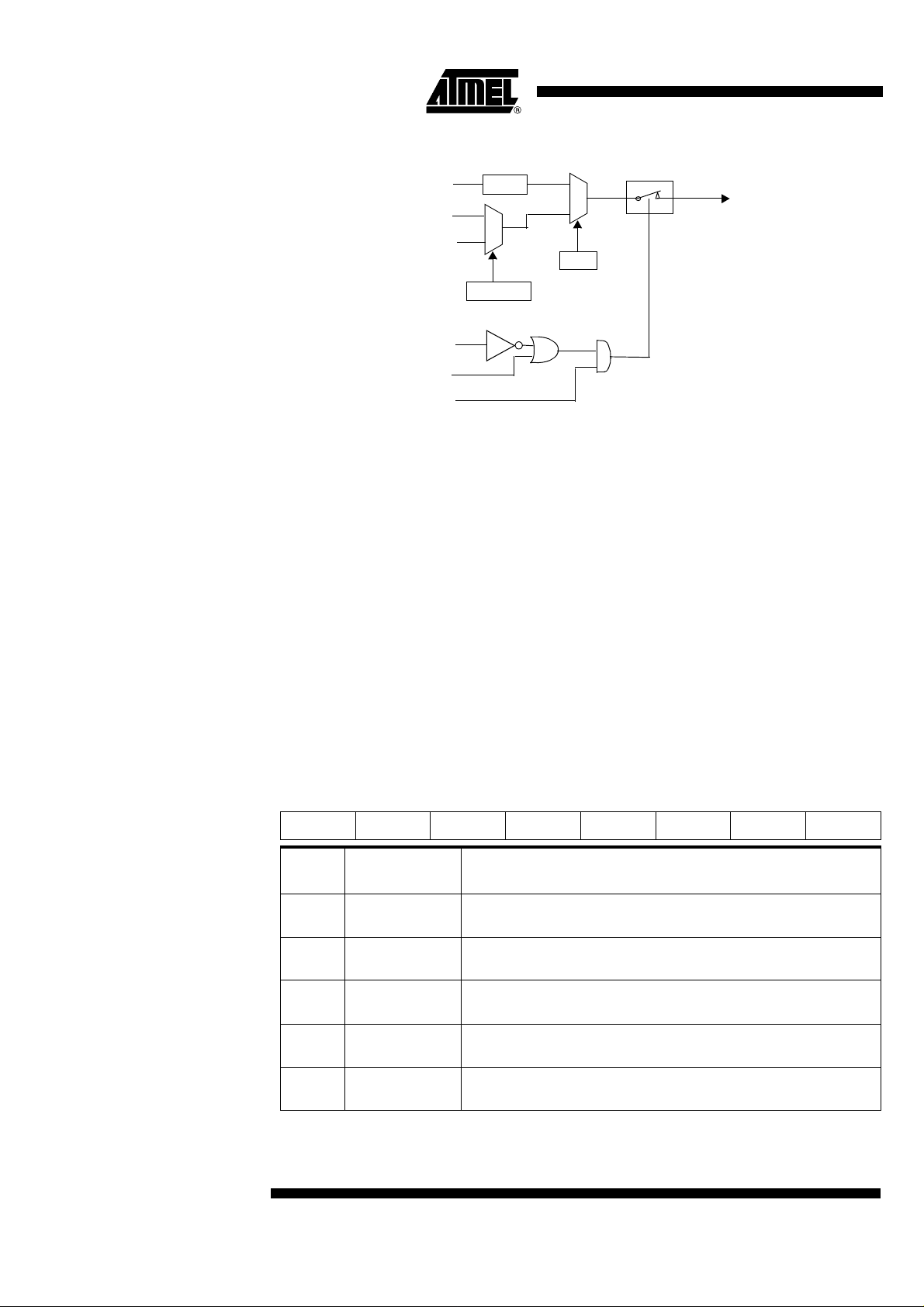
Clock System The AT8xC5111 oscillator system provides a reliable clocking system with full mastering
of speed versus CPU power trade off. Several clock sources are possible:
• External clock input
• High-speed crystal or ceramic oscillator
• Integrated high-speed RC oscillator
The selected clock source can be divided by 2 - 512 before clocking the CPU and the
peripherals. When X2 function is set, the CPU needs 6 clock periods per cycle.
Clocking is controlled by several SFR registers: OSCON, CKCON0, CKCON1, CKRL.
Blocks Description The AT8xC5111 includes the following oscillators:
• Crystal osci ll ator
• Integrated high-speed RC oscillator, with typical frequency of 12 MHz
Crystal Oscillator: OSCA The crystal oscillator uses two external pins, XTAL1 for input and XTAL2 for output.
Both crystal and ceramic resonators can be use d. An oscillator source on XTAL1 is
mandatory to start the product.
OSCAEN in OSCCON register is an enabl e signal for the crys tal oscill ator or the exte rnal oscillator input.
Integrated High-speed RC
Oscillator: OSCB
Clock Selector CKS bit in CKS register is used to select from crystal to RC oscillator.
Clock Prescaler Before supplying the CPU and the per iph eral s, the mai n cloc k is div ided by a fac tor of 2
The high-speed RC osci ll ato r typ ical fre que nc y i s 12 MHz. Note that the on c hi p osci ll ator has a ±50% frequency to lerance and may not be sui table for use in some
applications.
OSCBEN in OSCCON register is an enable signal for the high-speed RC oscillator.
OSCBEN bit in OSCCON register is used to enable the RC oscillator.
OSCAEN bit in OSCCON registe r is used to enable the crys tal oscilla tor or the ex terna l
oscillator input.
to 512, as defined by the CKRL register . The CPU need s from 12 to 256*12 c lock periods per instruction. This allows:
• to accept any cyclic ratio to be accepted on XTAL1 input.
• to reduce the CPU power consumption.
The X2 bit allows to bypass the clock prescaler; in this case, the CPU needs only 6 clock
periods per machine cycle. In X2 mode, as th is divider is bypassed, the signals on
XTAL1 must have a cyclic ratio between 40 to 60%.
4190A–8051–11/02
7

Functional Block Diagram
ResetB
Reload
: 128
Timer 0 Clock
Sub Clock
WD Clock
A/D Clock
CkAdc
Peripherals Clock
CkIdle
CPU Clock
Ck
Idle
Xtal1
Xtal2
OSCAEN
OSCBEN
Xtal_Osc
OSCA
PwdOsc
RC_Osc
OSCB
PwdRC
1
0
Mux
+
Filter
CKS
Ckrl
OscOut
8-bit
Prescaler-Divider
0
1
X2
CkOut
Quiet
Pwd
Operating Modes
Functional Modes
Normal Modes • CPU and Peripheral clocks depend on the software selection using CKCON0,
CKCON1, CKSEL and CKRL registers.
• CKS bit selects either Xtal_Osc or RC_Osc.
• CKRL register determines the frequency of the selected clock, unless X2 bit is set.
In this case the prescaler/divider is not used, so CPU core needs only 6 clock
periods per machine cycle. According to the value of the peripheral X2 individual bit,
each peripheral needs 6 or 12 clock periods per instruction.
• It is always possible to switch dynamically by software from Xtal_Osc to RC_Osc,
and vice versa by changing CKS bit, a synchronization cell allowing to avoid any
spike during transition.
Idle Modes • IDLE modes are achieved by using any instruction that writes into PCON.0 sfr
• IDLE modes A and B depend on previous software sequence, prior to writing into
PCON.0 register:
– IDLE MODE A: Xtal_Osc is running (OSCAEN = 1) and selected (CKS = 1)
– IDLE MODE B: RC_Osc is running (OSCBEN = 1) and selected (CKS = 0)
• The unused oscillator Xtal_Osc or RC_Osc can be stopped by software by clearing
OSCAEN or OSCBEN, respectively.
• Exit from IDLE mode is achieved by Reset, or by activation of an enabled interrupt.
• In both cases, PCON.0 is cleared by hardware.
8
AT8xC5111
4190A–8051–11/02

AT8xC5111
• Exit from IDLE modes will leave the oscillator control bits OSCAEN, OSCBEN and
CKS unchanged.
Power-down Modes • POWER-DOWN modes are achieved by using any instruction that writes into
PCON.1 sfr
• Exit from POWER-DOWN mode is achieved either by a hardware Reset, or by an
external interruption.
• By RST signal: The CPU will restart on OSCA.
• By INT0 or INT1 interruptions, if enabled. The oscillators control bits OSCAEN,
OSCBEN and CKS will not be changed, so the selected oscillator before entering
into Power-down will be activated.
Table 1. Power Modes
PD IDLE CKS OSCBEN OSCAEN S elected Mode Comment
0 0 1 X 1 NORMAL MODE A OSCA: XTAL clock
X X 1 X 0 INVALID No active clock
0 0 0 1 X NORMAL MODE B OSCB: high-speed RC clock
XX0 0 XINVALID
0 1 1 X 1 IDLE MODE A
0 1 0 1 X IDLE MODE B
1XX X X
TOTAL POWERDOWN
Prescaler Divi der • An hardware RESET selects the prescaler divider:
– CKRL = FFh: internal clock = OscOut/2 (Standard C51 feature)
– X2 = 0,
• After Reset, any value between FFh down to 00h can be written by software into
CKRL sfr in order to divide frequency of the selected oscillator:
– CKRL = 00h: minimum frequency = OscOut/512
– CKRL = FFh: maximum frequency = OscOut/2
The frequency of the CPU and peripherals clock CkOut is related to the frequency of the
main oscillator OscOut by the following formula:
F
CkOut
= F
/(512 - 2*CKRL)
OscOut
Some examples can be found in the table below:
F
OscOut
MHz X2 CKRL F
12 0 FF 6
The CPU is off, OSCA supplies the
peripherics
The CPU is off, OSCB supplies the
peripherics
The CPU is off, OSCA and OSCB are
stopped
(Mhz)
CkOut
4190A–8051–11/02
12 0 FE 3
12 1 x 12
• A software instruction which sets X2 bit de-activates the prescaler/divider, so the
internal clock is either Xtal_Osc or RC_Osc depending on SEL_OSC bit.
9
Timer 0: Clock Inputs
CkIdle
T0 pin
Sub Clock
Gate
INT0
TR0
: 6
0
1
SCLKT0
OSCCON
0
1
C/T
TMOD
Timer 0
Control
The SCLKT0 bit in OSCCON register allows to select Timer 0 Subsidiary clock. This
allows to perform a Real-Time Clock function.
SCLKT0 = 0: Timer 0 uses the standard T0 pin as clock input (Standard mode).
SCLKT0 = 1: Timer 0 uses the special Sub Clock as clock input.
When the subclock input is select ed for Time r 0 and the cr ystal os cillat or is sele ct ed for
CPU and peripherals , the CKRL pr escaler mu st be set to FF ( divisi on factor 2) in order
to assure a proper count on Timer 0.
With an external a 32 kHz oscillator, the timer interrupt can be set from 1/256 to 256
seconds to perform a Real-Time Clock (RTC) function. The power consumption will be
very low as the CPU is in idle mode at 32 kHz most of the time. When more CPU power
is needed, the internal RC oscillator is activated and used by the CPU and the others
peripherals.
Registers
Clock Control Register The clock control register is used to define the clock system behavior.
Table 2. OSCCON - Clock Control Register (8Fh)
76543210
-----SCLKT0OSCBENOSCAEN
Bit
Number
7-
6-
5-
4-
Bit
Mnemonic Description
Reserved
The value read from this bit is indeterminate. Do not set this bit.
Reserved
The value read from this bit is indeterminate. Do not set this bit.
Reserved
The value read from this bit is indeterminate. Do not set this bit.
Reserved
The value read from this bit is indeterminate. Do not set this bit.
10
AT8xC5111
3-
Reserved
The value read from this bit is indeterminate. Do not set this bit.
4190A–8051–11/02
AT8xC5111
Bit
Number
2SCLKT0
1OSCBEN
0OSCAEN
Bit
Mnemonic Description
Sub Clock Timer0
Cleared by software to select T0 pin
Set by software to select T0 Sub Clock
Enable RC oscillator
This bit is used to enable the high-speed RC oscillator
0: The oscillator is disabled
1: The oscillator is enabled.
Enable crystal oscillator
This bit is used to enable the crystal oscillator
0: The oscillator is disabled
1: The oscillator is enabled.
Reset value = 0XXX X001b
Not bit addressable
Clock Selection Register The clock selection register is used to define the clock system behavior
Table 3. CKSEL - Clock Selection Register (85h)
76543210
------CKS
Bit
Number
7-
6-
5-
4-
3-
2-
1-
0CKS
Bit
Mnemonic Description
Reserved
The value read from this bit is indeterminate. Do not set this bit.
Reserved
The value read from this bit is indeterminate. Do not set this bit.
Reserved
The value read from this bit is indeterminate. Do not set this bit.
Reserved
The value read from this bit is indeterminate. Do not set this bit.
Reserved
The value read from this bit is indeterminate. Do not set this bit.
Reserved
The value read from this bit is indeterminate. Do not set this bit.
Reserved
The value read from this bit is indeterminate. Do not set this bit.
Active oscillator selection
This bit is used to select the active oscillator.
1: The crystal oscillator is selected.
0: The high-speed RC oscillator is selected.
Reset value = XXXX XXX 1 b
Not bit addressable
4190A–8051–11/02
11

Clock Prescaler Register This register is used to reload the clock prescaler of the CPU and peripheral clock.
Table 4. CKRL - Clock Prescaler Register (97h)
76543210
M
Bit
Number
7: 0 CKRL
Bit
Mnemonic Descripti on
0000 0000b: Division factor equal 512
1111 1111b: Division factor equal 2
M: Division factor equal 2*(256-M)
Reset value = 1111 1111b
Not bit addressable
Clock Control Register This register is used to control the X2 mode of the CPU and peripheral clock.
Table 5. CKCON0 Register (8Fh)
76543210
- WdX2 PcaX2 SiX2 - T1X2 T0X2 X2
Bit
Number
7-Reserved
6WdX2
Bit
Mnemonic Description
Watchdog c lock (This control bit is validated when the CPU clock X2 is set; when
X2 is low, this bit has no effect)
Clear to select 6 clock periods per peripheral clock cycle.
Set to select 12 clock periods per peripheral clock cycle.
Programmable Counter Array clock (This control bit is validated when the CPU
5PcaX2
4SiX2
3-Reserved
2T1X2
1T0X2
clock X2 is set; when X2 is low, this bit has no effect)
Clear to select 6 clock periods per peripheral clock cycle.
Set to select 12 clock periods per peripheral clock cycle.
Enhanced UART clock (Mode 0 and 2) (This control bit is validated when the
CPU clock X2 is set; when X2 is low, this bit has no effect)
Clear to select 6 clock periods per peripheral clock cycle.
Set to select 12 clock periods per peripheral clock cycle.
Timer 1 clock (This control bit is validated when the CPU clock X2 is set; when X2
is low, this bit has no effect)
Clear to select 6 clock periods per peripheral clock cycle.
Set to select 12 clock periods per peripheral clock cycle
Timer 0 clock (This control bit is validated when the CPU clock X2 is set; when X2
is low, this bit has no effect)
Clear to select 6 clock periods per peripheral clock cycle.
Set to select 12 clock periods per peripheral clock cycle.
12
AT8xC5111
4190A–8051–11/02
AT8xC5111
Bit
Number
0X2
Bit
Mnemonic Description
CPU clock
Clear to select 12 clock periods per machine cycle (STD mode) for CPU and all the
peripherals.
Set to select 6clock periods per machine cycle (X2 mode) and to enable the
individual peripherals "X2" bits.
Reset value = X000 0000b
Not bit addressable
Table 6. CKCON1 Register (AFh)
7 6 5 43210
- - - ---BRGX2SPIX2
Bit
Number
7-Reserved
6-Reserved
5-Reserved
4-Reserved
Bit
Mnemonic Descripti on
3-Reserved
2-Reserved
BRG clock (This control bit is validated when the CPU clock X2 is set; when
1BRGX2
0 SPIX2
X2 is low, this bit has no effect).
Clear to select 6 clock periods per peripheral clock cycle.
Set to select 12 clock periods per peripheral clock cycle.
SPI clock (This control bit is validated when the CPU clock X2 is set; when X2
is low, this bit has no effect)
Clear to select 6 clock periods per peripheral clock cycle.
Set to select 12 clock periods per peripheral clock cycle.
Reset value = XXXX XX00 b
Not bit addressable
4190A–8051–11/02
13
AT8xC5111
Reset and Power
Management
The power monitoring and management can be used to supervise the Power Supply
(V
) and to start up properly when AT8xC5111 is powered up.
DD
It consists of the features listed below and explained hereafter:
• Power-off flag
• Idle mode
• Power-down mode
• Reduced EMI mode
All these features are controlled by several registers, the Power Control register (PCON)
and the Auxiliary register (AUXR) detailed at the end of this section.
AUX register not available on all versions.
Functional Description Figure 1 shows the block diagram of the possible sources of microcontroller reset.
Figure 1. Reset Sources
(1)
RST Pin
Hardware WD
RST Pin
Notes: 1. RST pin available only on 48 and 52 pins versions.
(2)
2. RST
PCA WD
pin available only on LPC versions.
Reset
Power-off Flag When the power is tur ned off or fails, the data retent ion is n ot guarant eed. A Pow er-off
Flag (POF, Table 8 on page 15) allows to det ect this conditi on. POF i s set by hard ware
during a reset wh ich follo ws a power-u p or a powe r-fail. Thi s is a cold reset. A war m
reset is an external or a watchdog reset without power failure, hence which preserves
the internal memory content and POF. To use POF, test and cl ear this bit just after
reset. Then it will be set only after a cold reset.
4190A–8051–11/02
14

Registers
PCON: Power Configuration
Register
Table 1. PCON Register (87h)
76543210
SMOD1 SMOD0 – POF GF1 GF0 PD IDL
Bit
Number
7SMOD1
6SMOD0
5 –
4POF
3GF1
Bit
Mnemonic Description
Double Baud Rate bit
Set to double the Baud Rate when Timer 1 is used and mode 1, 2 or 3 is
selected in SCON register.
SCON Select bit
When cleared, read/write accesses to SCON.7 are to SM0 bit and read/write
accesses to SCON.6 are to SM1 bit.
When set, read/write accesses to SCON.7 are to FE bit and read/write
accesses to SCON.6 are to OVR bit. SCON is Serial Port Control register.
Reserved
Must be cleared.
Power-off flag
Set by hardware when V
has been set off.
Must be cleared by software.
General Purpose flag 1
One use is to indicate wether an interrupt occurred during normal operation or
during Idle mode.
rises above V
DD
to indicate that the Power Supply
RET+
2GF0
1PD
0IDL
General Purpose flag 0
One use is to indicate wether an interrupt occurred during normal operation or
during Idle mode.
Power-down Mode bit
Cleared by hardware when an interrupt or reset occurs.
Set to activate the Power-down mode.
If IDL and PD are both set, PD takes precedence.
Idle Mode bit
Cleared by hardware when an interrupt or reset occurs.
Set to activate the Idle mode.
If IDL and PD are both set, PD takes precedence.
Reset value = 0000 0000b
Port Pins The value of port pins in the different operating modes is shown on Table 9.
Table 2. Pin Conditions in Special Operating Modes
Mode Program Memory Port 1 Pins Port 3 Pins Port 4 Pins
Reset Don’t care Weak High Weak High Weak High
Idle Internal Data Data Data
Power-down Internal Data Data Data
15
AT8xC5111
4190A–8051–11/02

AT8xC5111
Hardware Watchdog
Timer (WDT)
The WDT is intended as a recovery method in situations where the CPU may be subjected to software upset. The WDT consists of a 14-bit counter and the Watchdog Timer
Reset (WDTRST) SFR. The WDT is by defa ult disable d from exitin g reset. To e nable
the WDT, the user must write 01EH and 0E1H in sequ ence to the WDTRS T, SFR location 0A6H. When WDT is enabled, it will increment every machine cycle (6 internal clock
periods) and there is no way to disable the WDT except throu gh reset (eit her hardw are
reset or WD T ov erfl ow r es et). T he T0 bit of t he W DT PRG r egi ster is use d to se lec t th e
overflow after 10 or 14 bits. When WDT overflows, it will generate an i nternal reset. It
will also drive an output RESET HIG H pulse at the e mulator RS T-pin. T he lengt h of the
reset pulse is 24 clock periods of the WD clock.
Using the WDT To enable the WDT, the user must write 01E H and 0E1H in sequen ce to the WDTR ST,
SFR location 0A6H. When WDT is enabled, the user needs to service it by writing to
01EH and 0E1H to WDTRST to avoid WDT overflow. The 14-bit counter overflows when
it reaches 16383 (3FFFH) or 1024 (1 FFFH) and thi s will r es et the dev ice. W hen WDT is
enabled, it will increment every machine cycle while the oscillator is running. This means
the user must reset the WDT at least every 16383 machine cycle. To reset the WDT the
user must write 01EH and 0E1H to WDTRST. WDTRST is a write only register. The
WDT counter cannot be read or written. When WDT overflows, it will generate an output
RESET pulse at the RS T pin. The RESET pu lse duration is 96 x T
1/F
code that will periodically be executed within the time required to prevent a WDT reset.
To have a more powerful WDT, a 2
capability, ranking fr om 16 ms to 2s at F
ture, refer to WDTPRG register description, Table 11 (SFR0A7h).
. To make the best use of the W DT, it should b e servic ed in t hose se ctions of
OSC
7
counter has been added to extend the Time- out
= 12 MHz and T0 = 0. To manage this fea-
OSC
, where T
OSC
OSC
=
Table 1. WDT RS T Register
WDTRST Address (0A6h)
765 4 3 2 1
Reset value X X X X X X X
Write only, this SFR is used to reset/enable the WDT by writing 01EH then 0E1H in
sequence.
4190A–8051–11/02
16

Table 2. WDT PR G Regi st er
WDTPRG Address (0A7h)
76543210
T4 T3 T2 T1 T0 S2 S1 S0
Bit
Number
7T4
6T3
5T2
4T1
3T0
2 S2 WDT Time-out select bit 2
1 S1 WDT Time-out select bit 1
0 S0 WDT Time-out select bit 0
Bit
Mnemonic Description
Reserved
Do not try to set this bit.
WDT overflow select bit
0: Overflow after 14 bits
1: Overflow after 10 bits
S2
S1 S0 Selected Time-out with T0 = 0
000 (214 - 1) machine cycles, 16.3 ms at 12 MHz
001 (2
010 (2
011 (2
100 (2
101 (2
110 (2
111 (2
15
- 1) machine cycles, 32.7 ms at 12 MHz
16
- 1) machine cycles, 65.5 ms at 12 MHz
17
- 1) machine cycles, 131 ms at 12 MHz
18
- 1) machine cycles, 262 ms at 12 MHz
19
- 1) machine cycles, 542 ms at 12 MHz
20
- 1) machine cycles, 1.05 s at 12 MHz
21
- 1) machine cycles, 2.09 s at 12 MHz
Reset value = XXX0 0000
Write only register
WDT During Power-down and
Idle
Power-down In Power-down mode the oscill ator stops, whi ch means the W DT also stops . While in
Power-down mode the us er doe s not need to service the W DT . The re ar e 2 m etho ds of
exiting Power-down mode: by a hardware reset or via a level activated external interrupt
which is enabl ed p rio r to e nter ing Po wer-do wn mo de. W hen Powe r-down is e xite d wit h
hardware reset, servicing the WDT should occur as normal whenever the AT8xC5111 is
reset. Exiting Power-down with an interrupt is significantly different. The interrupt is held
low long enough for the oscillator to stabilize. Wh en the interru pt is brought hig h, the
interrupt is serviced. To prevent the WDT from resetting the device while the interrupt
pin is held low, the WDT is not started until the interrupt is pulled high. It is suggested
that the WDT be reset during the interrupt service routine.
To ensure that the WDT does not over flow wi thin a few sta tes of ex iting of power-down,
it is best to reset the WDT just before entering power-down.
Idle Mode In Idle mode, the oscillator continues to run. To prevent the WDT from resetting the
AT8xC5111 while in Idle mode, the user should always set up a timer that will periodically exit Idle, service the WDT, and re-enter Idle mode.
17
AT8xC5111
4190A–8051–11/02

AT8xC5111
Ports The low pin count versions of the AT8xC5111 has 3 I/O ports, port 1, port 3, and port 4.
All port1, port3 and port4 I/O port pins on the AT8xC5111 may be software configured to
one of four types o n a bi t-by-b it basis , as shown i n Tab le 13. T hese are: qua si b i-dire ctional (standard 80C51 port outputs), push-pull, open drain, and input only. Two
configuration registers for each port choose the output type for each port pin.
Table 1. Port Output Configuration Settings Using PxM1 and PxM2 Registers
PxM1.y Bit PxM2.y Bit Port Output Mode
0 0 Quasi bidirectional
0 1 Push-pull
1 0 Input Only (High Impedance)
1 1 Open Drain
Port Types
Quasi Bi-directional Output
Configuration
The default port output configuration for standard AT8xC5111 I/O ports is the quasi bidirectional outp ut that is c ommon on th e 80C5 1 and mos t of i ts d erivativ es. Th is o utput
type can be used as both an input and output without the need to reconfigure the port.
This is possible because when the port outputs a logic high, it is weakly driven, allowing
an external device to pull the pin low. When the pin is pulled low, it is driven strongly and
able to sink a fairly large current. These features are somewhat simil ar t o an op en drai n
output except that there are three pull-up transistors in the quasi-bidirectional output that
serve different purposes. One of these pull-ups, called the "very weak" pull-up, is turned
on whenever the port latch for the pin contains a logic 1. The very weak pull- up sou rces
a very small cur ren t t hat wil l pul l the pi n h igh i f i t i s lef t fl oat ing . A s ec ond pu ll -up, c al le d
the "weak" pull-up, is turned on when the port latch for the pin contains a logic 1 and the
pin itself is also at a logi c 1 level. This pull-up prov ides the prim ary sour ce current for a
quasi-bidirectiona l p in that is ou tputtin g a 1. If a pi n that h as a logi c 1 o n it i s pulle d low
by an external device, the weak pull-up turns off, and only the very weak pull-up remains
on. In order to pull the pin low under these cond itions, the external devi ce has to sink
enough current to ove rpower the weak pul l-up and take the vol tage on the port pin
below its input threshold.
The third pull-up is referred to as the "strong" pull-up. T his pull-up is used to speed up
low-to-high transitions on a quasi bi-directional port pin when the port latch changes
from a logic 0 to a lo gic 1. When this occur s, the strong pull-up turns o n fo r a b rief tim e,
two CPU clocks, in order to pull the port pin high quickly. Then it turns off again.
The quasi bi-directional port configuration is shown in Figure 2.
4190A–8051–11/02
18
Figure 1. Quasi bi-directional Output
Port Latch
Data
Open-drain Output
Configuration
Figure 2. Open-drain Output
Port Latch
Data
2 CPU
CLOCK DELAY
Input
Data
P
Strong
N
P
Very
Weak
P
Weak
Pin
The open-drain output configuration turns off all pull-ups and only drives the pull-down
transistor of the port driver when the port latch co ntains a logic 0. To be used as a logic
output, a port configur ed in thi s manne r must have an exter nal pul l-up , typical ly a resi stor tied to V
. The pull-down for this mode is the sam e as for the quasi bi-directional
DD
mode. The open-drain port configuration is shown in Figure 3.
Pin
N
Push-pull Output
Configuration
Input
Data
The push-pull output configuration has the same pull-down structure as both the open
drain and the quasi bi-directional output modes, but provides a continuous strong pullup when the port latch contain s a logic 1. Th e push-pul l mode may be used when mor e
source current is needed from a port output. The push-pull port configuration is shown in
Figure 4.
19
AT8xC5111
4190A–8051–11/02
Figure 3. Push-pull Output
AT8xC5111
P
Strong
Port latch
Data
Input
Data
Input Only Configuration The input only configuration is a pure input with neither pull-up nor pull-down.
The input only configuration is shown in Figure 5.
Figure 4. Input only
Input
Data
N
Pin
Pin
Ports Description
Ports P1, P3 and P4 Every output on the AT8xC5111 may potentially be used as a 20 mA sink LED drive out-
put. However, there is a maximu m total o utput curre nt for all p orts whic h must no t be
exceeded. All port pins of the AT8xC5111 have slew rate controlled outputs. This is to
limit noise g enerated b y quic kly s wit chin g outp ut si gnals . T he s lew rate is facto ry set to
approximately 10 ns rise and fall times.
The inputs of each I/O port of the AT8xC5111 are TTL level Schmitt triggers with
hysteresis.
Ports P0 and P2 The high pin-count version of the AT8xC5 111 has standard address and data ports P0
and P2. These ports are standard C51 po rts (Qua si bi-di rection al I/O). Th e control li nes
are provided on the pi ns: ALE, P SEN, EA
P1.1 and P1.0 .
4190A–8051–11/02
, Reset; RD and WR signals are on the bits
20

Registers Table 2. P1M1 Address (D4h)
76543210
P1M1.7 P1M1.6 P1M1.5 P1M1.4 P1M1.3 P1M1.2 P1M1.1 P1M1.0
Bit Number
7:0 P1M1.x
Bit
Mnemonic Description
Port Output configura tion bit
See Table 10. for configuration definition
Reset value = 0000 00XX
Table 3. P1M2 Address (E2h)
76543210
P1M2.7 P1M2.6 P1M2.5 P1M2.4 P1M2.3 P1M2.2 P1M2.1 P1M2.0
Bit Number
7:0 P1M2.x
Bit
Mnemonic Description
Port Output configura tion bit
See Table 10. for configuration definition
Reset value = 0000 00XX
Table 4. P3M1 Address (D5h)
76543210
P3M1.7 P3M1.6 P3M1.5 P3M1.4 P3M1.3 P3M1.2 P3M1.1 P3M1.0
Bit Number
7:0 P3M1.x
Bit
Mnemonic Description
Port Output configura tion bit
See Table 10 for configuration definition
Reset value = 0000 0000
Table 5. P3M2 Address (E4h)
76543210
P3M2.7 P3M2.6 P3M2.5 P3M2.4 P3M2.3 P3M2.2 P3M2.1 P3M2.0
Bit
Number
7:0 P3M2.x
Bit
Mnemonic Description
Port Output configura tion bit
See Table 10 for configuration definition
Reset value = 0000 0000
21
AT8xC5111
4190A–8051–11/02
AT8xC5111
Table 6. P4M1 Address (D6h)
76543210
P4M1.7 P4M1.6 P4M1.5 P4M1.4 P4M1.3 P4M1.2 P4M1.1 P4M1.0
Bit Number
7:0 P4M1.x
Bit
Mnemonic Description
Port Output configura tion bit
See Table 10. for configuration definition.
Reset value = 0000 0000
Table 7. P4M2 Address (E5h)
76543210
P4M2.7 P4M2.6 P4M2.5 P4M2.4 P4M2.3 P4M2.2 P4M2.1 P4M2.0
Bit Number
7:0 P4M2.x
Bit
Mnemonic Description
Port Output configura tion bit
See Table 10. for configuration definition.
Reset value = 0000 0000
4190A–8051–11/02
22
AT8xC5111
Dual Data Pointer
Register
Figure 1. Use of Dual Pointer
AUXR1(A2H)
The additional data pointer can be used to speed up code execution and reduce code
size in a number of ways.
The dual DPTR structure is a way by which the chip will specify the address of an external data memory location. There are two 16-bit DPTR registers that address the external
memory, and a single bit called DPS = AUXR1/bit0 (see Table 19) that allows the program code to switch between them (See Figure 6).
External Data Memory
07
DPS
DPTR1
DPTR0
DPH(83H) DPL(82H)
Table 1. AUXR1: Auxiliary Registe r 1
76543210
-------DPS
Bit
Number
7-
6-
5-
4-
3-
2-
1-
0DPS
Bit
Mnemonic Description
Reserved
The value read from this bit is indeterminate. Do not set this bit.
Reserved
The value read from this bit is indeterminate. Do not set this bit.
Reserved
The value read from this bit is indeterminate. Do not set this bit.
Reserved
The value read from this bit is indeterminate. Do not set this bit.
Reserved
The value read from this bit is indeterminate. Do not set this bit.
Reserved
The value read from this bit is indeterminate. Do not set this bit.
Reserved
The value read from this bit is indeterminate. Do not set this bit.
Data Pointer Selection
Clear to select DPTR0.
Set to select DPTR1.
Note: User software shoul d not wr ite 1s to res erved b its . These bit s may be us ed in fu ture 805 1
family products to invoke new features. In that case, the reset value of the new bit will be
0, and its active value will be 1. The value read from a reserved bit is indeterminate.
4190A–8051–11/02
23

Application Software can take advantage of the additional data pointers to both increase speed and
reduce code size, for example, block operations (copy, compare, search...) are well
served by using one data poin ter a s a ’source’ pointer and the oth er one as a "des tination" pointer.
ASSEMBLY LANGUAGE
; Block move using dual data pointers
; Destroys DPTR0, DPTR1, A and PSW
; note: DPS exits opposite of entry state
; unless an extra INC AUXR1 is added
;
00A2 AUXR1 EQU 0A2H
;
0000 909000MOV DPTR,#SOURCE ; address of SOURCE
0003 05A2 INC AUXR1 ; switch data pointers
0005 90A000 MOV DPTR,#DEST ; address of DEST
0008 LOOP:
0008 05A2 INC AUXR1 ; switch data pointers
000A E0 MOVX A,atDPTR ; get a byte from SOURCE
000B A3 INC DPTR ; increment SOURCE address
000C 05A2 INC AUXR1 ; switch data pointers
000E F0 MOVX atDPTR,A ; write the byte to DEST
000F A3 INC DPTR ; increment DEST address
0010 70F6JNZ LOOP ; check for 0 terminator
0012 05A2 INC AUXR1 ; (optional) restore DPS
INC is a short (2 bytes) and fast (12 clocks) way to manipulate the DPS bit in the AUXR1
SFR. However, note that the INC instruction does not directly force the DPS bit to a particular state, bu t simply togg les it. In simple routines , such as the block mov e examp le,
only the fact that DPS is togg led in th e pr op er se quen ce matt er s, n ot i ts a ctu al val ue. In
other words, th e block m ove rout ine work s the same whether DPS is '0' or '1' on en try.
Observe that without the last instruction (INC AUXR1), the routine will exit with DPS in
the opposite state.
24
AT8xC5111
4190A–8051–11/02
AT8xC5111
Serial I/O Ports
Enhancements
The serial I/O ports in the AT 8xC5111 are compatible with the serial I/O port in the
80C52.
They provide both synchronous and asynchronous communication modes. They operate as Univers al Asyn chrono us Recei ver a nd Transm itter (U ART) in three full-dupl ex
modes (modes 1, 2 and 3 ). A syn chro nous tr ansm iss ion and r ecep tion ca n occu r si multaneously and at different baud rates.
Serial I/O ports include the following enhancements:
• Framing error detection
• Automatic address recognition
Framing Error Detection Framing bit error detection is provided for the three asynchronous modes (modes 1, 2
and 3). To enable the framin g bi t erro r de tection feature, set SMOD0 bit in PCO N regi ster (see Figure 7).
Figure 1. Framing Error Block Diagram
SCON for UART (98h) (SCON_1 for UART_1 (C0h))
SM0/FE
SMOD0SMOD1
SM1
RENSM2
Set FE bit if stop bit is 0 (framing error) (SMOD0 = 1 for UART)
SM0 to UART mode control (SMOD0 = 0 for UART)
POF
-
GF1
RB8TB8
GF0
RITI
PCON for UART (87h) (SMOD bits for UART_1
IDLPD
are located in BDRCON_1)
Figure 2. UART Timings in Mode 1
RXD
RI
SMOD0 = X
FE
SMOD0 = 1
To UART framing error control
When this feature i s enabled, the receiv er c hec ks e ac h incoming data frame for a va li d
stop bit. An invalid stop bit may result from noise on the serial lines or from simultaneous
transmission by two CPUs. If a valid stop bit is not found, the Framing Error bit (FE) in
SCON register (see Table 25) bit is set.
Software may examine FE bit after each reception to check for data errors. Once set,
only software or a reset can clear FE bit. Subsequently received frames with valid stop
bits cannot clear FE b it. W hen FE featur e is enab led, RI rise s on st op bit i nstead of th e
last data bit (see Figure 8 and Figure 9).
D7D6D5D4D3D2D1D0
Start
Bit
Data Byte
Stop
Bit
4190A–8051–11/02
25

Figure 3. UART Timings in Modes 2 and 3
RXD
D8D7D6D5D4D3D2D1D0
Automatic Address
Recognition
Start
Bit
Data Byte Ninth
Bit
Stop
Bit
RI
SMOD0 = 0
RI
SMOD0 = 1
FE
SMOD0 = 1
The automatic address recognition feature is enabled for each UART when the multiprocessor communication feature is enabled (SM2 bit in SCON register is set).
Implemented i n hardwa re, au tomati c addre ss reco gnition enhan ces the m ultip roces sor
communication feature by allowing the serial port to examine the address of each
incoming command frame. Only when the serial port re cognizes it s own address, the
receiver sets RI bit in SCON register to generate an interrupt. This ensures that the CPU
is not interrupted by command frames addressed to other devices.
If desired, you may enabl e the automatic address re cognition fea ture in mode 1. In this
configuration, the stop bit takes the place of the ninth data bit. Bit RI is set only when the
received command frame address matches the device’s addre ss and is te rminated by a
valid stop bit.
To support automatic a ddr ess re co gni tio n, a dev ic e i s identified by a given add re ss and
a broadcast address.
Note: The multiprocessor communication and automatic address recognition features cannot
be enabled in mode 0 (i.e., setting SM2 bit in SCON register in mode 0 has no effect).
Given Address Each UART has an individual ad dress that is sp ecified in SADDR r egiste r; the SA DEN
register is a mask byte that contains don’t care bits (defined by zeros) to form the
device’s given address. The don’t care bits provide the flexibility to address one or more
slaves at a time. The following example illustrates how a given address is formed.
To address a device by its individual address, the SADEN mask byte must be 1111
1111b.
For example:
SADDR0101 0110b
SADEN
1111 1100b
Given0101 01XXb
The following is an example of how to use given addresses to address different slaves:
Slave A:SADDR1111 0001b
SADEN
1111 1010b
Given1111 0X0Xb
Slave B:SADDR1111 0011b
Slave C:SADDR1111 0010b
1111 1001b
SADEN
Given1111 0XX1b
SADEN
1111 1101b
Given1111 00X1b
26
AT8xC5111
4190A–8051–11/02

AT8xC5111
The SADEN byte is selected so that each slave may be addressed separately.
For slave A, bit 0 (the LSB) is a don’t care bit; for slav es B a nd C, bit 0 is a 1. T o co mmu-
nicate with slave A only, the master must send an address where bit 0 is clear (e.g.
1111 0000b).
For slave A, bit 1 is a 1; for slaves B and C, bit 1 is a don’t care bit. To communicate with
slaves B and C, but not slave A, the master must send an address with bits 0 and 1 both
set (e.g. 1111 0011b).
To communicate with slaves A, B and C, the master must send an address with bit 0
set, bit 1 clear, and bit 2 clear (e.g. 1111 0001b).
Broadcast Address A broadcast address is formed from the logical OR of the SADDR and SADEN registers
with zeros defined as don’t care bits, e.g.:
SADDR 0101 0110b
SADEN 1111 1100b
Broadcast = SADDR OR SADEN1111 111Xb
The use of don’t care bits provides flexibility in defining the broadcast address, however
in most applications, a broadcast address is FFh. The following is an example of using
broadcast addresses:
Slave A:SADDR1111 0001b
SADEN
1111 1010b
Broadcast1111 1X11b,
Slave B:SADDR1111 0011b
Slave C:SADDR = 1111 0010b
1111 1001b
SADEN
Broadcast1111 1X11B,
1111 1101b
SADEN
Broadcast1111 1111b
For slaves A and B, bit 2 is a don’t care bit; for slave C, bit 2 is set. To communicate with
all of the slaves, the ma ster must se nd an add ress F Fh. To c ommun icate with sl aves A
and B, but not slave C, the master can send and address FBh.
Reset Addresses On reset, the SADDR and SADEN registers are initialized to 00h, i.e. the given and
broadcast addresses ar e XXXX XXXXb (all don’t car e bits). Thi s ensure s that the seria l
port will reply to any address, and so, that it is backwar ds compatible with the 80C5 1
microcontrollers that do not support automatic address recognition.
Baud Rate Selection for
UART for Modes 1 and 3
The Baud Rate Generator for transmit and receive clocks can be selected separately via
the T2CON and BDRCON registers.
4190A–8051–11/02
27

Figure 4. Baud Rate Selection
INT_BRG
RBCK
TIMER1_BRG
0
1
/ 16
Rx Clock
Internal Baud Rate Generator
(BRG)
TIMER1_BRG
INT_BRG
TBCK
0
1
/ 16
Tx Clock
Table 1. Baud Rate Selection Table for UART
Clock Source
TBCK RBC K Clock Source for UART Tx
0 0 Timer 1 Timer 1
10 INT_BRG Timer 1
0 1 Timer 1 INT_BRG
1 1 INT_BRG INT_BRG
UART Rx
When the internal B au d Ra te Generator is used, t he Bau d Ra tes a re de ter mi ned by th e
BRG overflow depend ing on the B RL re load v alue, the X2 bit i n CKON0 regi ster, the
value of SPD bit (Sp eed Mod e) in BDRC ON registe r and t he value o f the SM OD1 bi t in
PCON regist e r (for UART).
28
AT8xC5111
Figure 5. Internal Baud Rate Generator
SMOD1
Peripheral Clock
SPD
BRR
/6
Auto Reload Counter
0
1
BRG
BRL
/2
Overflow
0
INT_BRG
1
4190A–8051–11/02

for UART:
Baud_Rate =
SMOD1
2
2 x 2 x 6
X2
x 2
x F
XTAL
(1-SPD)
x 16 x [256 - (BRL)]
AT8xC5111
(BRL) = 256 -
SMOD1
2
2 x 2 x 6
(1-SPD)
X2
x 2
x F
XTAL
x 16 x Baud_Rate
Example of computed value when X2 = 1, SMOD1 = 1, SPD = 1
F
= 16.384 MHz F
Baud Rates
115200 247 1.23 243 0.16
57600 238 1.23 230 0.16
38400 229 1.23 217 0.16
28800 220 1.23 204 0.16
19200 203 0.63 178 0.16
9600 149 0.31 100 0.16
4800 43 1.23 - -
XTAL
BRL Error (%) BRL Error (%)
XTAL
Example of computed value when X2 = 0, SMOD1 = 0, SPD = 0
F
= 16.384 MHz F
Baud Rates
4800 247 1.23 243 0.16
OSC
BRL Error (%) BRL Error (%)
OSC
= 24 MHz
= 24 MHz
2400 238 1.23 230 0.16
1200 220 1.23 202 3.55
600 185 0.16 152 0. 16
The baud rate generator can be used for mode 1 or 3 (See Figure 10), but also for mode
0 for both UARTs, thanks to the bit SRC located in BDRCON register (see Table 27).
4190A–8051–11/02
29

UART Registers Table 2. SADEN - Slave Address Mask Register for UART (B9h)
76543210
Reset value = 0000 0000b
Table 3. SADDR - Slave Address Register for UART (A9h)
76543210
Reset value = 0000 0000b
Table 4. SBUF - Serial Buffer Register for UART (99h)
76543210
Reset value = XXXX XXX Xb
T able 5. BRL - Baud Rate Reload Register for the Internal Baud Rate Generator, UART
- UART(9Ah)
76543210
Reset value = 0000 0000b
30
AT8xC5111
4190A–8051–11/02

AT8xC5111
Table 6. SCON Register
SCON - Serial Control Register for UART (98h)
76543210
FE/SM0 SM1 SM2 REN TB8 RB8 TI RI
Bit
Number
7FE
6SM1
5SM2
4REN
3TB8
Bit
Mnemonic Description
SM0
Framing Error bit (SMOD0 = 1) for UART
Clear to reset the error state, not cleared by a valid stop bit.
Set by hardware when an invalid stop bit is detected.
SMOD0 must be set to enable access to the FE bit
Serial Port Mode bit 0 (SMOD0 = 0) for UART
Refer to SM1 for serial port mode selection.
SMOD0 must be cleared to enable access to the SM0 bit
Serial Port Mode bit 1 for UART
SM1 Mode Description Baud Rate
SM0
0 0 0 Shift Register F
0 1 1 8-bit UART Variable
10 2 9-bit UART F
1 1 3 9-bit UART Variable
Serial Port Mode 2 bit/Multiprocessor Communication Enable bit for UART
Clear to disable multiprocessor communication feature.
Set to enable multiprocessor communication feature in mode 2 and 3, and
eventually mode 1. This bit should be cleared in mode 0.
Reception Enable bit for UART
Clear to disable serial reception.
Set to enable serial reception.
Transmitter Bit 8/Ninth bit to transmit in modes 2 and 3 for UART.
Clear to transmit a logic 0 in the 9th bit.
Set to transmit a logic 1 in the 9th bit.
XTAL
XTAL
/12 (F
/64 or F
/6 X2 mode)
XTAL
/32 (F
XTAL
XTAL
/32 or F
/16 X2 mode)
XTAL
4190A–8051–11/02
Receiver Bit 8/Ninth bit received in modes 2 and 3 for UART
2RB8
1TI
0RI
Cleared by hardware if 9th bit received is a logic 0.
Set by hardware if 9th bit received is a logic 1.
In mode 1, if SM2 = 0, RB8 is the received stop bit. In mode 0 RB8 is not used.
Transmit Interrupt flag for UART
Clear to acknowledge interrupt.
Set by hardware at the end of the 8th bit time in mode 0 or at the beginning of the
stop bit in the other modes.
Receive Interrupt flag for UART
Clear to acknowledge interrupt.
Set by hardware at the end of the 8th bit time in mode 0, see Figure 8 and Figure 9
in the other modes.
Reset value = 0000 0000b
Bit addressable
31

Table 7. PCON Register
PCON - Power Control Register (87h)
76543210
SMOD1 SMOD0 RSTD POF G F1 GF0 PD IDL
Bit
Number
7SMOD1
6SMOD0
5RSTD
4POF
3GF1
2GF0
1PD
Bit
Mnemonic Description
Serial Port Mode bit 1 for UART
Set to select double baud rate in mode 1, 2 or 3.
Serial Port Mode bit 0 for UART
Clear to select SM0 bit in SCON register.
Set to to select FE bit in SCON register.
Reset Detector Disable Bit
Clear to disable PFD.
Set to enable PFD.
Power-off Fla g
Clear to recognize next reset type.
Set by hardware when VCC rises from 0 to its nominal voltage. Can also be set
by software.
General-purpose Flag
Cleared by user for general purpose usage.
Set by user for general purpose usage.
General-purpose Flag
Cleared by user for general purpose usage.
Set by user for general purpose usage.
Power-down Mode bit
Cleared by hardware when reset occurs.
Set to enter Power-down mode.
Idle Mode bit
0IDL
Clear by hardware when interrupt or reset occurs.
Set to enter idle mode.
Reset value = 0001 0000b
Not bit addressable
Power-off flag reset value will be 1 only after a power on (cold reset). A warm reset
doesn’t affect the value of this bit.
32
AT8xC5111
4190A–8051–11/02

AT8xC5111
Table 8. BDRCON Register
BDRCON - Baud Rate Control Register (9Bh)
76543210
- - - BRR TBCK RBCK SPD SRC
Bit
Number
7-
6-
5-
4BRR
3TBCK
2RBCK
1SPD
0SRC
Bit
Mnemonic Description
Reserved
The value read from this bit is indeterminate. Do not set this bit.
Reserved
The value read from this bit is indeterminate. Do not set this bit.
Reserved
The value read from this bit is indeterminate. Do not set this bit.
Baud Rate Run Control bit
Clear to stop the internal Baud Rate Generator.
Set to start the internal Baud Rate Generator.
Transmission Baud rate Generator Selection bit for UART
Clear to select Timer 1 or Tim er 2 for the Baud Rate Generator.
Set to select internal Baud Rate Generator.
Reception Baud Rate Generator Selection bit for UART
Clear to select Timer 1 or Tim er 2 for the Baud Rate Generator.
Set to select internal Baud Rate Generator.
Baud Rate Speed Control bit for UART
Clear to select the SLOW Baud Rate Generator.
Set to select the FAST Baud Rate Generator.
Baud Rate Source Select bit in Mode 0 for UART
Clear to select F
Set to select the internal Baud Rate Generator for UARTs in mode 0.
/12 as the Baud Rate Generator (F
OSC
/6 in X2 mode).
OSC
4190A–8051–11/02
Reset value = XXX0 0000b
33

AT8xC5111
Serial Port Interface
(SPI)
The Serial Peripheral Interface (SPI) module which allows full-duplex, synchronous,
serial communication between the MCU and peripheral devices, including other MCUs.
Features Features of the SPI module include the following:
• Full-duplex, three-wire synchronous transfers
• Master operation
• Eight programmable Master clock rates
• Serial clock with programmable polarity and phase
• Master Mode fault error flag with MCU interrupt capability
• Write collision flag protection
Signal Description Figure 12 shows a typical SPI bus configuration using one Master controller and many
Slave peripherals. The bus is made of three wires connecting all the devices:
Figure 1. Typical SPI bus
Slave 1
MISO
MOSI
SCK
SS
Master
MISO
MOSI
SCK
SS
PORT
V
DD
0
1
2
3
MISO
MOSI
SCK
MISO
MOSI
Slave 4
SCK
SS
MISO
MOSI
Slave 3
SCK
SS
Slave 2
SS
The Master device selects the individual Slave devices by using four pins of a parallel
Master Output Slave Input
(MOSI)
port to control the four SS
This 1-bit signal is directly connected between the Master Device and a Slave Device.
The MOSI line is used to transfer data in series from the Master to the Slave. Therefore,
pins of the Slave devices.
it is an output signal fr om the M as ter , a nd a n in put si gna l to a S la ve . A b yt e ( 8-bi t wor d)
is transmitted most significant bit (MSB) first, least significant bit (LSB) last.
Master Input Slave Output
(MISO)
This 1-bit signal is directly connected between the Slave Device and a Master Device.
The MISO line is used to transfer data in series from the Slave to the Master. Therefore,
it is an output signal from the Slave, and an input signal to the Master. A byte (8-bit
word) is transmitted most significant bit (MSB) first, least significant bit (LSB) last.
SPI Serial Clock (SCK) This signal is used to synchronize the data movement both in and out the devices
through their MOSI and MISO lines. It i s driven by the Master for eight clock cycles
which allows to exchange one byte on the serial lines.
Slave Select (SS
) Each Slave peripheral is selected by one Slave Select pin (SS). This signal must stay
low for any message for a Slav e. It is obvi ous that on ly one Ma ster (S S
high level) can
drive the network. The Master may select each Slave device by software through port
4190A–8051–11/02
34

pins (see Figure 12). To prevent bus conflicts on the MISO line, only one slave should
be selected at a time by the Master for a transmissi on .
In a Master configurati on, the SS
line can be used in conju nctio n with the M ODF flag i n
the SPI Status register (SPSTA) to prevent multiple masters from driving MOSI and
SCK (see Error Conditions).
Baud Rate In Master mode, the baud rate can be selected from a baud rate generator which is con-
troled by three bits in the SPCON register: SPR2, SPR1 and SPR0. The Master clock is
chosen from one of seven c lock r ates res ulting from the divi sion o f the inte rnal cl ock by
2, 4, 8, 16, 32, 64 or 128, or an external clock.
Table 28 gives the different clock rates selected by SPR2:SPR1:SPR0.
Table 1. SPI Master Baud Rate Selection
SPR2:SPR1:SPR0 Clock Rate Baud Rate Divisor (BD)
000 F
001 F
010 F
011 F
100 F
101 F
110 F
111 External clock Output of BRG
/2 2
CkIdle
/4 4
CkIdle
/8 8
CkIdle
/16 16
CkIdle
/32 32
CkIdle
/64 64
CkIdleH
/128 128
CkIdle
35
AT8xC5111
4190A–8051–11/02

Functional Description Figure 13 shows a detailed structure of the SPI module.
Figure 2. SPI Module Block Diagram
Internal Bus
SPDAT
AT8xC5111
CkIdle
Clock
Divider
External Clk
SPI Interrupt Request
/128
/2
/4
/8
/16
/32
/64
Clock
Select
Shift Register
234567
01
Receive Data Register
Clock
Logic
CPHA
SPR1
CPOLMSTRSSDISSPENSPR2
SPR0
SPCON
SPI
Control
- ----
SPIF
WCOL
MODF
Pin
Control
Logic
M
S
MOSI
MISO
SCK
SS
8-bit Bus
1-bit Signal
SPSTA
Operating Modes The Serial Peri pheral Inter face can be conf igur ed as Mast er mod e onl y. Th e con figur a-
tion and initialization of the SPI module is made through one register:
• The Serial Peripheral CONtrol register (SPCON)
Once the SPI is configured, the data exchange is made using:
• SPCON
• The Serial Peripheral STAtus register (SPSTA)
• The Serial Peripheral DATa register (SPDAT)
During an SPI transmiss i on, da ta is s im ult ane ous ly tr ans mi tted (shi fted out ser i all y) an d
received (shifted in serially ). A s erial clock line (SCK ) synchroni zes sh ifting and sampling on the two serial data lines (MOSI and MISO).
When the Master device transmits data to the Slave device via the MOSI line, the Slave
device responds by sending data to the Master device via the MISO line. T his implies
full-duplex transmission with both data out and data in synchronized with the same clock
(Figure 14).
4190A–8051–11/02
36

Figure 3. Full-Duplex Master-slave Interc onn ec tio n
MISOMISO
MOSI
VSS
8-bit Shift register
SSSS
Slave MCU
SPI
Clock Generator
Master MCU
8-bit Shift register
MOSI
SCK SCK
VDD
Master Mode The SPI operate s in M aster mo de. Onl y one Ma ster S PI devi ce ca n initiate trans mis-
sions. Software begins the transmission from a Master SPI module by writing to the
Serial Peripheral Data Register (SPDAT). If the shift register is empty, the byte is immediately transferred to the shift register. The byte begins shifting out on MOSI pin under
the control of t he serial cloc k, SCK. S imultaneously , another b yte shifts in from the
Slave on the Master’s MISO pin. The transmi ssion ends when the Serial P eripheral
transfer data flag, SPIF, in SPSTA becomes set. At the same time that SPIF becomes
set, the received byte from the Slave is transferred to the receive data register in
SPDAT. Software clea rs SPIF by readin g the Seria l Peri pheral S tatus r egister (SPST A)
with the SPIF bit set, and then reading the SPDAT.
When the pin SS is pulled down during a transmission, the data is interrupted and when
the transmission is established again, the data present in the SPDAT is present.
Transmission Formats Software can select any of four combinations of serial clock (SCK) phase and polarity
using two bits in the SPCON: the Clock POLarity (CPOL
(CPHA
(1)
). CPOL defines the default SCK line level in idle state. It has no significant
(1)
) and the Clock PHAse
effect on the transmission format. CPHA defi nes the edges on whi ch the input da ta are
sampled and the edg es on whi ch the output d ata are s hifted (Figur e 15 and Figure 16).
The clock phase and polarity should be identical for the Master SPI device and the communicating Slave device.
Figure 4. Data Transmission Format (CPHA = 0)
13245678
MSB bit6 bit5 bit4 bit3 bit2 bit1 LSB
37
SCK Cycle Number
SPEN (Internal)
SCK (CPOL = 0)
SCK (CPOL = 1)
MOSI (from Master)
MISO (from Slave)
(to Slave)
SS
Capture Point
AT8xC5111
1. Before writing to the CPOL and CPHA bits, the SPI should be disabled (SPEN = ’0’).
bit6 bit5 bit4 bit3 bit2 bit1MSB
LSB
4190A–8051–11/02

Figure 1 6 shows an SPI transmission in which CPHA is ’1’. In this case, the Master
begins driving its MOSI pin on the first SCK edge. Therefore the Slave uses the first
SCK edge as a start transmission signal . Th e S S
sions (Figure 17). This format may be preferable in systems having only one Master and
only one Slave driving the MISO data line.
Figure 5. Data Transmission Format (CPHA = 1)
AT8xC5111
pin can remain low between transmis-
SCK Cycle Number
SPEN (Internal)
SCK (CPOL = 0)
SCK (CPOL = 1)
MOSI (from Ma ster)
MISO (from Slave)
SS
Capture Poi nt
Figure 6. CPHA/SS
(to Slave)
Timing
132 45678
MSB bit6 bit5 bit4 bit3 bit2 bit1 LSB
MSB LSB
bit6 bit5 bit4 bit3 bit2 bit1
Figure 15 shows the first SCK edge is th e MSB capt ure strob e. Theref ore, the S lave
must begin driving its data before the first SCK edge, and a falling edge on the SS
used to start the trans mission. The SS
pin must be toggle d high and the n low betw een
each byte transmitted (Figure 17).
MISO/MOSI
Master SS
Slave SS
(CPHA = 0)
Slave SS
(CPHA = 1)
Byte 1 Byte 2
Byte 3
pin is
4190A–8051–11/02
38

Error Conditions The following flags in the SPSTA signal SPI error conditions:
Mode Fault (MODF) Mode Fault error in Master mode SPI indicates that the level on the Slave Select (SS
pin is inconsistent with the actual mode of the device. MODF is set to warn that there
may be a multi-mas ter conflict for syst em control. In this case, the SPI syste m is
affected in the following ways:
• An SPI receiver/error CPU interrupt request is generated.
• The SPEN bit in SPCON is cleared. This disables the SPI.
• The MSTR bit in SPCON is cleared.
The MODF flag is set when the SS
However, as stated before, for a system with one Master, if the SS
device is pull ed low, there is no way that anot her Mas ter is att empti ng to dri ve the net work. In this case, clearing the MODF bit is accomplished by a read of SPSTA register
with MODF bit set, followed by a write to the SP CO N regi ste r. SPEN Cont ro l bit may be
restored to its original set state after the MODF bit has been cleared.
Write Collision (WCOL) A Write Collision (WCOL) flag in the SPSTA is set when a write to the SPDAT register is
done during a transmit sequence.
WCOL does not cause an interruption, and the transfer continues uninterrupted.
Clearing the WCOL bi t is done thro ugh a softwa re sequenc e of an access to SPSTA
and an access to SPDAT.
Overrun C ondition An overrun condition occ urs when the Mas ter devic e trie s to send sever al data by tes
and the Slave device has not cleared the SPIF bit issuing from the previous data byte
transmitted. In this case, the receiver buffer contains the byte sent after the SPIF bit was
last cleared. A read of the SPDAT returns this byte. All others bytes are lost.
signal becomes ’0’.
pin of the Ma ster
)
This condition is not detected by the SPI peripheral.
Interrupts Two SPI status flags can generate a CPU interrupt request:
Table 2. SPI Inte rrup ts
Flag Request
SPIF (SP data transfer) SPI Transmitter Interrupt request
MODF (Mode Fault) SPI Receiver/Error Interrupt Request (if SSDIS = ’0’)
Serial Peripheral data tran sfer flag, SPIF: This bit is set by hardware when a trans fer
has been completed. SPIF bit generates transmitter CPU interrupt requests.
Mode Fault flag, MODF: This bit becomes set to indicate that the level on the SS
inconsistent with the mode of the SPI. MODF generates receiver/error CPU inte rrupt
requests.
is
39
AT8xC5111
4190A–8051–11/02

Figure 18 gives a logical view of the above statements.
Figure 7. SPI Interrupt Requests Generation
AT8xC5111
SPIF
MODF
SSDIS
SPI Transmitter
CPU Interrupt Request
SPI Receiver/Err or
CPU Interrupt Request
SPI
CPU Interrupt Request
4190A–8051–11/02
40

Registers There are three registers in the module that provide control, status and data storage
functions. These registers are described in the following paragraphs.
Serial Peripheral Control
Register (SPCON)
The Serial Peripheral Control Register does the following:
• Selects one of the Master clock rates
• Selects serial clock polarity and phase
• Enable s the SP I modul e
Table 30 describes this register and explains the use of each bit:
Table 3. Serial Peripheral Control Register
76543210
SPR2 SPEN ––CPOL CPHA SPR1 SPR0
Bit
Number
7SPR2RW
6SPENRW
5-RW
4-RW
Bit
Mnemonic R/W Mode Description
Serial Peripheral Rate 2
Bit with SPR1 and SPR0 define the clock rate
Serial Peripheral Enable
Clear to disable the SPI interface
Set to enable the SPI interface
Reserved
Leave this Bit at 0.
Reserved
Leave this Bit at 1.
3CPOLRW
2CPHARW
1SPR1RW
0SPR0RW
Reset value = 00010100b
Clock Polarity
Clear to have the SCK set to ’0’ in idle state
Set to have the SCK set to ’1’ in idle low
Clock Phase
Clear to have the data sampled when the SPSCK leaves the idle
state (see CPOL)
Set to have the data sampled when the SPSCK returns to idle
state (see CPOL)
Serial Peripheral Rate (SPR2:SPR1:SPR0)
CkIdle
CkIdle
CkIdle
CkIdle
CkIdle
CkIdle
CkIdle
/2
/4
/8
/16
/32
/64
/128
000: F
001: F
010: F
011: F
100: F
101: F
110: F
111: External clock, output of BRG
41
AT8xC5111
4190A–8051–11/02

AT8xC5111
Serial Peripheral Status Register
(SPSTA)
The Serial Peripheral Status Register contains flags to signal the following conditions.
• Data transfer complete
• Write collision
• Inconsistent logic level on SS
pin (mode fault error)
Table 31 describes the SPSTA register and explains the use of every bit in the register:
Table 4. Serial Peripheral Status and Control Register
76543210
SPIFWCOL-MODF----
Bit
Number
7SPIFR
6WCOLR
5-RW
Bit
Mnemonic
R/W
Mode Description
Serial Peripheral data transfer flag
Cleared by hardware to indicate data that transfer is in progress or has
been approved by a clearing sequence.
Set by hardware to indicate that the data transfer has been completed.
Write Collision flag
Cleared by hardware to indicate that no collision has occurred or has
been approved by a clearing sequence.
Set by hardware to indicate that a collision has been detected.
Reserved
The value read from this bit is indeterminate. Do not set this bit
4MODFR
3-RW
2-RW
1-RW
0-RW
Reset value = 00X0XXXXb
Mode Fault
Cleared by hardware to indicate that the SS
level, or has been approved by a clearing sequence.
Set by hardware to indicate that the SS
level
Reserved
The value read from this bit is indeterminate. Do not set this bit
Reserved
The value read from this bit is indeterminate. Do not set this bit
Reserved
The value read from this bit is indeterminate. Do not set this bit
Reserved
The value read from this bit is indeterminate. Do not set this bit
pin is at appropriate logic
pin is at inappropriate logic
4190A–8051–11/02
42

Serial Peripheral Data Register
(SPDAT)
The Serial Peripheral Data Register (Table 32) is a read/write buffer for the receive data
register. A write to SPDAT pla ces data di rectly into the shift reg ister. No tran smit buffer
is available in this model.
A Read of the SPDAT returns the value located in the receive buffer and not the content
of the shift register.
Table 5. Serial Peripheral Data Register
76543210
R7 R6 R5 R4 R3 R2 R1 R0
Reset value = XXXX XXX Xb
R7:R0: Receive data bits
SPCON, SPSTA and S PDAT r egister s m ay be r ead an d written at any time while th ere
is no on-going exchange. However, special care should be taken when writing to them
while a transmission is on-going:
• Do not change SPR2, SPR1 and SPR0
• Do not change CPHA and CPOL
• Do not change MSTR
• Clearing SPEN would immediately disable the peripheral
• Writing to the SPDAT will cause an overflow
43
AT8xC5111
4190A–8051–11/02

AT8xC5111
Programmable
Counter Array (PCA)
The PCA provides more timing capabilities with less CPU intervention than the standard
timer/counters. Its advantages include reduced software overhead and improved accuracy. The PCA cons ists of a de dicate d timer/ counter which se rves as the time ba se for
an array of five c ompare /capt ure mod ules. It s cloc k input c an be pr ogramm ed to co unt
any one of the following signals:
• Oscillator frequency
• Oscillator frequency
• Timer 0 overflow
• External input on ECI (P1.2)
Each compare/capture modules can be programmed in any one of the following modes:
• rising and /or falling edg e captu re
• software timer
• high-speed output
• pulse width modulator
Module 4 can also be programmed as a watchdo g timer (see Section "PCA PW M
Mode", page 53).
When the compare/capture modules are programmed in the capture mode, software
timer, or high-spee d outp ut mod e, a n i nte rru pt can be generated when th e m odu le ex ecutes its functio n. All five modules pl us the PCA timer over flow share one interr upt
vector.
The PCA timer/counter and compare/capture modules share Port 1 for external I/O.
These pins are listed below. If the port is not used for the PCA, it c an still be used for
standard I/O.
÷ 12 (÷ 6 in X2 mode)
÷ 4 (÷ 2 in X2 mode)
PCA Component External I/O Pin
16-bit Counter P1.2/ECI
16-bit Module 0 P1.3/CEX0
16-bit Module 1 P1.4/CEX1
16-bit Module 2 P1.5/CEX2
16-bit Module 3 P1.6/CEX3
16-bit Module 4 P1.7/CEX4
The PCA timer is a common time base for all five modules (see Figure 19). The timer
count source is determined from the CPS1 and CPS0 bits in the CMOD SFR (see
Table 33) and can be programmed to run at:
• 1/12 the oscillator frequency. (Or 1/6 in X2 Mode).
• 1/4 the oscillator frequency. (Or 1/2 in X2 Mode).
• The Timer 0 overflow.
• The input on the ECI pin (P1.2).
4190A–8051–11/02
44

Figure 1. PCA Timer/Counter
Fosc /12
Fosc/4
T0 OVF
P1.2
CH CL
16-bit Up/Down Counter
overflow
To PCA
Modules
It
Idle
CIDL CPS1 CPS0 ECF
WDTE
CF CR
CCF4 CCF3 CCF2 CCF1 CCF0
CMOD
0xD9
CCON
0xD8
Table 1. CMOD: PCA Counter Mode Register - CMOD Address 0D9H
76543210
CIDL WDTE - - - CPS1 CPS0 ECF
Bit
Number
Bit
Mnemonic Description
Counter Idle control:
7CIDL
CIDL = 0 programs the PCA Counter to continue functioning during idle Mode.
CIDL = 1 programs it to be gated off during idle.
Watchdog Timer Enable:
6WDTE
WDTE = 0 disables Watchdog Tim er function on PCA Module 4. WDTE = 1
enables it.
5 - Not implemented, reserved for future use.
(1)
4 - Not implemented, reserved for future use.
3 - Not implemented, reserved for future use.
/12 ( Or f
osc
/4 ( Or f
osc
(2)
osc
/2 in X2 Mode).
osc
/6 in X2 Mode).
CPS1
0 0 Internal clock f
2CPS1
0 1 Internal clock f
CPS0 Selected PCA input
1 0 Timer 0 Overflow
1 1 External clock at ECI/P1.2 pin (max rate = f
osc
/ 8)
1 CPS0 PCA Count Pulse Select bit 0.
0ECF
PCA Enable Counter Overflow interrupt: ECF = 1 enables CF bit in CCON to
generate an interrupt. ECF = 0 disables that function of CF.
Reset value = 00XXX00
45
AT8xC5111
1. User software should not write 1s to res erved b its . These bit s may be us ed in fu ture 805 1
family products to invoke new features. In that case, the rese t or inactive value of the
new bit will be 0, and its active value will be 1.The value read from a reserved bit is
indeterminate.
2. f
= oscillator frequency
osc
4190A–8051–11/02

AT8xC5111
The CMOD SFR includes three additional bits associated with the PCA (See Figure 19
and Table 33).
• The CIDL bit which allows the PCA to stop during idle mode.
• The WDTE bit which enables or disables the watchdog function on module 4.
• The ECF bit which when set causes an interrupt and the PCA overflow flag CF (in
the CCON SFR) to be set when the PCA timer overflows.
The CCON SFR contains the run cont rol bi t for the PCA and the flag s for the PC A timer
(CF) and each module (see Table 34).
• Bit CR (CCON.6) must be set by software to run the PCA. The PCA is shut off by
clearing this bit.
• Bit CF: The CF bit (CCON.7) is set when the PCA counter overflows and an
interrupt will be generated if the ECF bit in the CMOD register is set. The CF bit can
only be clear ed by software.
• Bits 0 through 4 are the flags for the modules (bit 0 for module 0, bit 1 for module 1,
etc.) and are set by hardware when either a match or a capture occurs. These flags
also can only be cleared by software.
Table 2. CCON: PCA Counter Control Register
CCON Address OD8H
76543210
CF CR - CCF4 CCF3 CCF2 CCF1 CCF0
Bit
Number
7CF
6CR
5 - Not implemented, reserved for future use
4 CCF4
3 CCF3
2 CCF2
1 CCF1
0 CCF0
Bit
Mnemonic Description
PCA Counter Overflow flag. Set by hardware when the counter rolls over. CF flags
an interrupt if bit ECF in CMOD is set. CF may be set by either hardware or
software but can only be cleared by software.
PCA Counter Run control bit. Set by software to turn the PCA counter on. Must be
cleared by software to turn the PCA counter off.
PCA Module 4 interrupt flag. Set by hardware when a match or capture occurs.
Must be cleared by software.
PCA Module 3 interrupt flag. Set by hardware when a match or capture occurs.
Must be cleared by software.
PCA Module 2 interrupt flag. Set by hardware when a match or capture occurs.
Must be cleared by software.
PCA Module 1 interrupt flag. Set by hardware when a match or capture occurs.
Must be cleared by software.
PCA Module 0 interrupt flag. Set by hardware when a match or capture occurs.
Must be cleared by software.
(1)
.
1. User software should not write 1s to res erved b its . These bit s may be us ed in fu ture 805 1
family products to invoke new features. In that case, the reset or inactive value of the
new bit will be 0, and its active value will be 1. The value read from a reserved bit is
indeterminate.
4190A–8051–11/02
The watchdog timer function is implemented in module 4 (see Figure 22).
46

Figure 2. PCA Interrupt System
The PCA interrupt system is shown in Figure 20 below.
PCA Timer/Counter
Module 0
Module 1
Module 2
Module 3
Module 4
CCON
0xD8
To Interrupt
priority decoder
ECF
CF CR
ECCFn
CCF4 CCF3 CCF2 CCF1 CCF0
CCAPMn.0CMOD.0
IE.6 IE.7
EC EA
PCA Modules: each one of t he five compare /capture modules has si x possib le fun ctions. It can perform:
• 16-bit Capture, positive-edge triggered
• 16-bit Capture, negative-edge triggered
• 16-bit Capture, both positive and negative-edge triggered
• 16-bit Software Timer
• 16-bit High-speed Output
• 8-bit Pulse Width Modulator
47
In addition, module 4 can be used as a Watchdog Timer.
Each module in the PCA has a s peci al functi on reg ister ass ocia ted with it. T hese regis-
ters are: CCAPM0 for module 0, CCAPM1 for module 1, etc. (see Table 35). The
registers contain the bits that control the mode that each module will operate in.
• The ECCF bit (CCAPMn.0 where n = 0, 1, 2, 3, or 4 depending on the module)
enables the CCF flag in the CCON SFR to generate an interrupt when a match or
compare occurs in the associated module.
• PWM (CCAPMn.1) enables the pulse width modulation mode.
• The TOG bit (CCAPMn.2) when set causes the CEX output associated with the
module to toggle when there is a match between the PCA counter and the module's
capture/compare register.
• The match bit MAT (CCAPMn.3) when set will cause the CCFn bit in the CCON
register to be set when there is a match between the PCA counter and the module's
capture/compare register.
• The next two bits CAPN (CCAPMn.4) and CAPP (CCAPMn.5) determine the edge
that a capture input will be active on. The CAPN bit enables the negative edge, and
the CAPP bit enables the positive edge. If both bits are set both edges will be
enabled and a capture will occur for either transition.
AT8xC5111
4190A–8051–11/02

AT8xC5111
• The last bit in the register ECOM (CCAPMn.6) when set enables the comparator
function.
Table 35 shows the CCAPMn settings for the various PCA functions.
Table 3. CCAPMn: PCA Modules Compare/Capture Control Registers
CAPMn Address n = 0 - 4
76543210
- ECOMn CAPPn CAPn MATn TOGn PWMm ECCFn
Bit
Number
7 - Not implemented, reserved for future use.
6 ECOMn Enable Comparator. ECOMn = 1 enables the comparator function.
5 CAPPn Capture Positive, CAPPn = 1 enables positive edge capture.
4 CAPNn Capture Negative, CAPNn = 1 enables negative edge capture.
3MATn
2TOGn
1PWMn
0 ECCFn
Bit
Mnemonic Description
(1)
Match. When MATn = 1, a match of the PCA counter with this module’s
compare/capture register causes the CCFn bit in CCON to be set, flagging an
interrupt.
Toggle. When TOGn = 1, a match of the PCA counter with this module’s
compare/capture register causes the CEXn pin to toggle.
Pulse Width Modulation Mode. PWMn = 1 enables the CEXn pin to be used as a
pulse width modulated output.
Enable CCF interrupt. Enables compare/capture flag CCFn in the CCON register
to generate an interrupt.
Reset value = X000000
1. User software should not write 1s to res erved b its . These bit s may be us ed in fu ture 805 1
family products to invoke new features. In that case, the reset or inactive value of the
new bit will be 0, and its active value will be 1. The value read from a reserved bit is
indeterminate.
4190A–8051–11/02
Table 4. PCA Module Modes (CCAPMn Registers)
ECOMn CAPPn CAPNn MATn TOGn PWMm ECCFn Module Function
0000000No Operation
X10000X
X01000X
X11000X
100100X
1 0 0 1 1 0 X 16-bit High-speed Output
10000108-bit PWM
1 0 0 1 X 0 X Watchdog Timer (module 4 only)
16-bit capture by a positive-edge
trigger on CEXn
16-bit capture by a negative trigger
on CEXn
16-bit capture by a transition on
CEXn
16-bit Software Timer/Compare
mode.
48

There are two additional registers associated with each of the PCA modules. They are
CCAPnH and CCAPnL and these are the registers that store the 16-bit co unt when a
capture occurs or a compare should occur. When a module is used in the PWM mode
these registers are used to control the duty cycle of the output (See Table 37 &
Table 38)
Table 5. CCAPnH: PCA Modules Capture/Compare Registers High
CCAP0H = 0FAH
CCAPnH Address
n = 0 - 4
Table 6. CCAPnL: PCA Modules Capture/Compare Registers Low
CCAPnL Address
n = 0 - 4
CCAP1H = 0FBH
CCAP2H = 0FCH
CCAP3H = 0FDH
CCAP4H = 0FEH
76543210
Reset value 00000000
CCAP0L = 0EAH
CCAP1L = 0EBH
CCAP2L = 0ECH
CCAP3L = 0EDH
CCAP4L = 0EEH
Reset value 00000000
Table 7. CH: PCA Counter High
CH
Address 0F9H
Reset value 00000000
Table 8. CL: PCA Counter Low
CL
Address 0E9H
Reset value 00000000
76543210
76543210
76543210
49
AT8xC5111
4190A–8051–11/02

AT8xC5111
PCA Capture Mode To use one of the PCA mo dules in the captu re mode either one or both o f the CCAPM
bits CAPN and CAPP f or tha t mo dul e m us t be s et. Th e ex te rnal CEX i nput for th e m odule (on port 1) is sampled for a transition. When a valid transition occurs the PCA
hardware loads the value of the PCA counter registers (CH and CL) into the module’s
capture registers (CCAPnL and CCAPn H). If the CC Fn bit for the m odule in the CCON
SFR and the ECCFn bit in the CCAPMn SFR are set then an interrupt will be generated
(see Figure 21).
Figure 3. PCA Capture Mode
Cex.n
CF CR
ECOMn
CCF4 CCF3 CCF2 CCF1 CCF0
Capture
CAPNn MATn TOGn PWMn ECCFnCAPPn
CCON
0xD8
PCA IT
PCA Counter/Timer
CH CL
CCAPnH CCAPnL
CCAPMn, n = 0 to 4
0xDA to 0xDE
4190A–8051–11/02
50

16-bit Software Timer/
Compare Mode
The PCA modules can be used as software timer s by setting both the ECOM and MAT
bits in the modules CCAPMn regi ster. The PCA timer will be compared to the module’s
capture registers and when a match occurs an interrupt will occur if the CCFn (CCON
SFR) and the ECCFn (CCAPMn SFR) bits for the module are both set (See Figure 22).
Figure 4. PCA Compare Mode and PCA Watchdog Timer
CF CCF2 CCF1 CC F0
CR
Write to
CCAPnH
Write to
CCAPnL
10
Reset
CCAPnH CCAPnL
Enable
16-bit Comparator
CH CL
PCA Counter/Timer
ECOMn
CCF4
Match
CAPNn MATn TOGn PWMn ECCFnCAPPn
CCF3
CCON
0xD8
PCA IT
(1)
RESET
CCAPMn, n = 0 to 4
0xDA to 0xDE
Note: 1. Only for Module 4
CIDL CPS1 CPS0 ECF
WDTE
CMOD
0xD9
Before enabling ECO M bi t, CCA P nL a nd CC AP nH s hou ld be s et with a non zero value,
otherwise an unwanted match could occur. Writing to CCAPnH will set the ECOM bit.
Once ECOM is set, writing CCAPnL will clear ECOM so that an unwanted match doesn’t
occur while modifying the compare value. Writing to CCA PnH will set ECOM. For this
reason, user software should write CCAPnL first, and then CCAPnH. Of course, the
ECOM bit can still be controlled by accessing to CCAPMn register.
51
AT8xC5111
4190A–8051–11/02

AT8xC5111
High-speed Output Mode In this mode the CEX output (on port 1) associated with the PCA module will toggle
each time a match occurs between the PCA counter and the module’s capture registers.
To activate this mode the TOG, MAT, and ECOM bits in the module’s CCAPMn SFR
must be set (see Figure 23).
A prior write must be done to CCAPnL and CCAPnH before writing the ECOMn bit.
Figure 5. PCA High-speed Output Mode
CCON
0xD8
PCA IT
Write to
CCAPnH
Write to
CCAPnL
Reset
CF CR
CCAPnH CCAPnL
CCF4 CCF3 CCF2 CCF1 CCF0
0
1
Pulse Width Modulator
Mode
Enable
16-bit Comparator
CH CL
PCA Counter/Timer
ECOMn
Match
CAPNn MATn TOGn PWMn ECCFnCAPPn
CEXn
CCAPMn, n = 0 to 4
0xDA to 0xDE
Before enabling ECO M bi t, CCA P nL a nd CC AP nH s hou ld be s et with a non zero value,
otherwise an unwanted match could happen.
Once ECOM is set, writing CCAPnL will clear ECOM so that an unwanted match doesn’t
occur while modifying the compare value. Writing to CCA PnH will set ECOM. For this
reason, user software should write CCAPnL first, and then CCAPnH. Of course, the
ECOM bit can still be controlled by accessing to CCAPMn register.
All of the PCA module s can b e used a s PWM out puts. F igure 24 sh ows the PW M function. The frequen cy of t he output depends on the source fo r the P CA time r. All o f the
modules will hav e the sam e freque ncy of outpu t beca use they al l share th e PCA tim er.
The duty cycle of each module is independently variable using the module's capture
register CCAPLn. When the value of the PCA CL SFR is less than the value in the module's CCAPLn SFR the output will be low , wh en it i s eq ual to o r gr ea ter th an, the output
will be high. When CL overflows from FF to 00, CCAP Ln is reloaded with the value i n
CCAPHn. This allows updati ng the PWM wi thout glitch es. The PWM and ECOM bits in
the module's CCAPMn register must be set to enable the PWM mode.
4190A–8051–11/02
52

Figure 6. PCA PWM Mode
CCAPnH
CCAPnL
8-bit Comparator
CL
PCA Counter/Timer
“0”
<
>
“1”
CCAPMn, n = 0 to 4
0xDA to 0xDE
CEXn
ECOMn
Overflow
Enable
CAPNn MATn TOGn PWMn ECCFnCAPPn
An on-board watchdog ti mer is availab le with the PCA to imp rove the rel iability of th e
system without increasing chip count. Watchdog timers are useful for systems that are
susceptible to noise, power glitches, or electrostatic discharge. Module 4 is the only
PCA module that can be programmed as a watchdog. However, this module can still be
used for other modes i f the watchd og i s n ot ne eded . F igur e 22 shows a di agram of h ow
the watchdog works. The us er pre-loads a 16-bit v alue in the compare reg isters. Jus t
like the other compare modes, this 16-bit value is compared to the PCA timer value. If a
match is allowed to occ ur, an interna l reset will be gener ated. This wi ll not cause the
RST pin to be driven high.
53
In order to hold off the reset, the user has three options:
1. Periodically change the compare value so it will never match the PCA timer
2. Periodically change the PCA timer value so it will never match the compare values or
3. Disable the watchdog by clearing the WDTE bit before a match occurs and then
re-enable it
The first two options are more rel iab le becaus e the watc hdog tim er is ne ve r dis abled as
in option #3. If the program coun ter ever goes astray, a mat ch will eve ntually oc cur and
cause an internal res et. T he se co nd o pti on i s als o n ot r ecommended if other PCA m odules are being used. Remember, the PCA timer is the time base for all modules;
changing the time base for other modules would not be a good idea. Thus, in most applications the first solution is the best option.
This watchdog timer won’t generate a reset out on the reset pin.
AT8xC5111
4190A–8051–11/02

AT8xC5111
Analog-to-Digital
Converter (ADC)
This section describes the on-chip 10-bit analog-to-digital converter of the
T89C51RB2/RC2. Eight ADC channels are avai lable for sampling of the external
sources AN0 to AN7. An analog multiplexer allows the single ADC to select one of the 8
ADC channels as ADC inp ut voltage (ADCIN). A DCIN is c onverted by the 10 bit-ca scaded potentiometric ADC.
Three kind of conversions are avai la ble :
• Standard conversion (7-8 bits).
• Precision conversion (8-9 bits).
• Accurate conversion (10 bits).
For the precision conversion, set bits PSIDLE and A DSST in ADCON register to start
the conversion. The c hip i s in a pseudo- idle mode , the CPU do esn’t run but t he peri pherals are always running. This mode allows digital noise to be lower, to ensure precise
conversion.
For the accurate conversion, set bits QUIETM and ADSST in ADCON register to start
the conversion . The chi p is in a q uiet mode, the AD i s th e on ly p eriphe ral runn ing. This
mode allows digital noise to be as low as possible, to ensure high precision conversion.
For these modes it is necessary to work with end of conversion interrupt, which is the
only way to wake up the chip.
If another interrupt occurs during the precision con version, it will be treated only after
this conversion is ended.
Features • 8 channels with multiplexed inputs
• 10-bit cascaded potentiometric ADC
• Conversion time down to 10 micro-seconds
• Zero Error (offset) ± 2 LSB max
• External Positive Reference Voltage Range 2.4 to V
• ADCIN Range 0 to V
• Integral non-linearity typical 1 LSB, max. 2 LSB (with 0.9*VCC<V
• Differential non-linearity typical 0.5 LSB, max. 1 LSB (with 0.9*V
• Conversion Complete Flag or Conversion Complete Interrupt
• Selected ADC Clock
CC
CC
REF<VCC
CC<VREF<VCC
)
)
ADC I/O Functions AINx are general I/Os that are shared with the ADC channels. The channel select bits in
ADCF register define which AD C channel pin will be used as ADCIN. The remaining
ADC channels pins can be used as general pur pose I/Os or as the al ternate func tion
that is available. Writes to the port register which aren’t selected by the ADCF will not
have any effect.
4190A–8051–11/02
54

Figure 1. ADC Description
ADCON.5
ADEN
ADCON.3
ADSST
CONV_CK
AIN0/P4.0
AIN1/P4.1
AIN2/P4.2
AIN3/P4.3
AIN4/P4.4
AIN5/P4.5
AIN6/P4.6
AIN7/P4.7
000
001
010
011
100
101
110
111
SCH2
ADCON.2
ADCON.4
ADEOC
CONTROL
ADC
Interrupt
Request
EADC
IE1.1
8
2
10
ADDH
ADDL
Sample an d H old
SCH1
ADCON.1
AVSS
SCH0
ADCON.0
ADCIN
ADCON.5
VADREF
+
SAR
-
R/2R DAC
VAGND
ADEN
Vref
Figure 26 shows the timing diagram of a com plete con version. F or simpl icity, the figure
depicts the waveforms in ideal ized form and does n ot provide pr ecise timin g information. For ADC characteristics and timing parameters refer to the Section “AC
Characteristics” of the AT8xC5111 datasheet.
Figure 2. Timing Diagram
CONV_CK
ADEN
ADSST
ADEOC
Note: Tsetup = 4 µ s
T
SETUP
T
CONV
55
AT8xC5111
4190A–8051–11/02

AT8xC5111
ADC Operation Before starting a conversion, the A/D converter must be enabled, by setting the ADEN
bit, for at least T
A start of single A/D conversion is triggered by setting bit ADSST (ADCON.3).
From the ADSST set, the first full CONV_CK period will be the sampling period for the
ADC; during this period , the swit ch is close d and the capaci tor is bein g charged. At the
end of the first period, the switch opens and the capacitor is no longer being charged.
During the next 10 CO NV_CK pe ri od s, the sa mpl e a nd hol d will b e i n h old mo de dur in g
the conversion. The busy flag ADSST(ADCON.3) remains set as long as an A/D conversion is running. After compl etion of the A/D conversion, it is cl ear ed by har dwar e . Whe n
a conversion is running, this flag can be read only, a write has no effect.
The end-of-conversion flag ADEOC (ADCON.4) is set when the value of conversion is
available in ADDH and ADDL, it is cleared by software. If the bit EADC (IE1.1) is set, an
interrupt occur when flag ADEOC is set (see Figure 28). Clear this flag for re-arming the
interrupt.
From this point, if you keep starting a new conversion by resetting ADSST without
changing ADEN, it is not necessary to wait T
The bits SCH0 to SCH2 in ADCON register are used for the analog input channel
selection.
(four microseconds).
setup
setup
.
Before starting nor mal power re duction modes the ADC co nversion ha s to be c ompleted.
Table 1. Selected Analog Input
SCH2 SCH1 SCH0 Selected Analog Input
000AN0
001AN1
010AN2
011AN3
100AN4
101AN5
110AN6
111AN7
Voltage Conversion When the ADCIN is equal to VAREF, the ADC co nv er ts the sig nal to 3 FF h (ful l s c ale ). If
the input voltage equals VAGND, the ADC converts it to 000h. Input vol tage between
VA REF a nd VAGND are a straight-line linear co nver sion . All oth er voltages will resu lt in
3FFh if greater than VAREF and 000h if less than VAGND.
Note that ADCIN should not exceed VAREF absolute maximum range.
4190A–8051–11/02
56

Clock Selection The maximum clock fre quenc y fo r AD C (CONV _CK for C onvers ion Clo ck) i s de fined in
the AC characteristics section. A prescaler is featured (ADCCLK) to generate the
CONV_CK clock from the oscillator frequency.
Figure 3. A/D Converter Clock
CONV_CK
CKADC
/2
The conversion frequency CONV_CK is derived from the oscillator frequency with the
following formulas:
F
CkAdc
= F
= F
/(512 - 2*CKRL) , if X2 = 0
OscOut
OscOut
and
Prescaler ADCLK
A/D
Converter
, if X2 = 1
F
CONV_CK
F
CONV_CK
= F
= F
/(2*PRS), if PRS > 0
CkAdc
/256, if PRS = 0
CkAdc
Some examples can be found in the table below:
ADC Standby Mode
F
OscOut
MHz X2 CKRL
16 0 FF 8 12 333 33
16 1 NA 16 32 250 44
F
CkAdc
Mhz ADCLK
When the ADC is not used, it is po ssible to set it in s tandby mode by cl eari ng bit ADEN
in ADCON register.
In this mode the power dissipation is about 1 µW.
F
CONV_CK
khz
Conversion
time µs
Voltage Reference The Vref pin is used to enter the voltage reference for the A/D conversion.
Best accuracy is obtained with 0.9 V
CC
< V
REF
< VCC.
IT ADC Management An interrupt end-of-conversion will occur when the bit ADEOC is acti vated and the bit
EADC is set. To re-arm the interrupt the bit ADEOC must be cleared by software.
57
AT8xC5111
Figure 4. ADC Interrupt Structure
ADEOC
ADCON.2
ADCI
EADC
IE1.1
4190A–8051–11/02

Registers Table 2. ADCON Register
ADCON (S:F3h)
ADC Control Register
76543210
QUIETM PSIDLE ADEN ADEOC ADSST SCH2 SCH1 SCH0
Bit Number Bit Mnemonic Description
AT8xC5111
7QUIETM
6PSIDLE
5ADEN
4ADEOC
3ADSST
2 - 0 SCH2:0
Reset value = X000 0000b
Table 3. ADCLK Register
ADCLK (S:F2h)
ADC Clock Prescaler
Pseudo Idle mode (best precision)
Set to put in quiet mode during conversion.
Cleared by hardware after completion of the conversion.
Pseudo Idle mode (good precision)
Set to put in idle mode during conversion.
Cleared by hardware after completion of the conversion.
Enable/Standby Mode
Set to enable ADC.
Clear for Standby mode (power dissipation 1 µW).
End Of Conversion
Set by hardware when ADC result is ready to be read. This flag can
generate an interrupt.
Must be cleared by software.
Start and Status
Set to start an A/D conversion.
Cleared by hardware after completion of the conversion.
Selection of channel to convert
See Table 41.
4190A–8051–11/02
76543210
- PRS 6 PRS 5 PRS 4 PRS 3 PRS 2 PRS 1 PRS 0
Bit Number Bit Mnemonic Description
7 –
6 - 0 PRS6:0
Reserved
Leave this bit at 0.
Clock Prescaler
= f
f
CONV_CK
if PRS = 0, f
CkADC
CONV_CK
/(2 * PRS)
= f
CkADC
/256
Reset value = 0000 0000b
58

Table 4. ADDH Register
ADDH (S:F5h Read Only)
ADC Data High byte register
76543210
ADAT 9 ADAT 8 ADAT 7 ADAT 6 ADAT 5 ADAT 4 ADAT 3 ADAT 2
Bit Number Bit Mnemonic Description
7 - 0 ADAT 9:2
ADC result
Bits 9 - 2
Read only register
Reset value = 00h
Table 5. ADDL Register
ADDL (S:F4h Read Only)
ADC Data Low byte register
76543210
- - - - - - ADAT 1 ADAT 0
Bit Number Bit Mnemonic Description
7 - 6 -
1 - 0 ADAT1:0
Reserved
The value read from these bits are indeterminate. Do not set these bits.
ADC result
Bits 1 - 0
Read only register
Reset value = xxxx xx00b
Table 6. ADCF Register
59
AT8xC5111
ADCF (S:F6h)
ADC Input Select Register
76543210
SEL7 SEL6 SEL5 SEL4 SEL3 SEL2 SEL1 SEL0
Bit Number Bit Mnemonic Description
7 - 0 SEL7 - 0
Select Input 7 - 0
Set to select bit 7 - 0 as possible input for A/D
Cleared to leave this bit free for other function
4190A–8051–11/02

AT8xC5111
Interrupt System The AT8xC5111 has a total of 8 interrupt vectors: two external interrupts (INT0 and
INT1
), two timer interrupts (timers 0, 1), serial port interrupt, PCA, SPI and A/D. These
interrupts are shown in Figure 29.
Figure 1. Interrupt Control System
IPH, IP
High Priority
Interrupt
INT0
TF0
INT1
TF1
PCA
RI
TI
ADC
NC
SPI
CF
CCFx
IE0
IE1
3
0
3
0
3
0
3
0
3
0
3
0
3
0
3
0
3
0
Interrupt
Polling
Sequence
4190A–8051–11/02
Individual
Enable
Global
Disable
Low Priority
Interrupt
Each of the interrupt sources can be individually enabled or disabled by setting or clearing a bit in the Interrup t Enable reg ister (See Tab le 49). This reg ister also con tains a
global disable bit, which must be cleared to disable all interrupts at once.
Each interrupt sou rce can als o be indivi dually pr ogramme d to one of four pri ority le vels
by setting or clearing a bit in the Interrupt Priority register (See Table 51) and in the
Interrupt Priority High register (see Table 53). Table 47 shows the bit values and priority
levels associated with each combination.
60

Table 1. Priority Bit Level Values
IPH.x IP.x Interrupt Level Priority
0 0 0 (Lowest)
011
102
1 1 3 (Highest)
A low-priority inte rrupt can be int errupt ed by a high prior ity i nterru pt, b ut no t by an other
low-priority interrupt. A high-priority inte rrupt can’t be interrupted by any other interrupt
source.
If two interrupt requests of different priority levels are received simultaneously, the
request of higher prio rity lev el is servi ced. If interr upt req uests of th e same prio rity le vel
are received simultaneously, an internal polling sequence determines which request is
serviced. Thus within each priority level there is a second priority structure determined
by the polling sequence.
Table 2. Address Vectors
Interrupt Name Interrupt Address Vector Priority Number
External Interrupt (INT0) 0003h 1
Timer0 (TF0) 000Bh 2
External Interrupt (INT1) 0013h 3
Timer1 (TF1) 001Bh 4
PCA (CF or CCFn) 0033h 5
UART (RI or TI) 0023h 6
SPI 004Bh 8
ADC 0043h 9
61
AT8xC5111
4190A–8051–11/02

AT8xC5111
Table 3. IE0 Register
IE0 - Interrupt Enable Register (A8H)
76543210
EA EC - ES ET1 EX1 ET0 EX0
Bit
Number
7EA
6EC
5-
4ES
3ET1
2EX1
1ET0
Bit
Mnemonic Description
Enable All interrupt bit
Clear to disable all interrupts.
Set to enable all interrupts.
If EA = 1, each interrupt source is individually enabled or disabled by setting or
clearing its interrupt enable bit.
PCA Interrupt Enable
Clear to disable the the PCA interrupt.
Set to enable the the PCA interrupt.
Reserved
The value read from this bit is indeterminate. Do not set this bit.
Serial port Enable bit
Clear to disable serial port interrupt.
Set to enable serial port interrupt.
Timer 1 overflow interrupt Enable bit
Clear to disable timer 1 overflow interrupt.
Set to enable timer 1 overflow interrupt.
External interrupt 1 Enable bit
Clear to disable external interrupt 1.
Set to enable external interrupt 1.
Timer 0 overflow interrupt Enable bit
Clear to disable timer 0 overflow interrupt.
Set to enable timer 0 overflow interrupt.
4190A–8051–11/02
0EX0
External interrupt 0 Enable bit
Clear to disable external interrupt 0.
Set to enable external interrupt 0.
Reset value = 00X0 0000b
Bit addressable
62

Table 4. IE1 Register
IE1 (S:B1H) - Interrupt Enable Register
76543210
-----ESPIEADC-
Bit
Number
7-
6-
5-
4-
3-
2 ESPI
1EADC
0-
Bit
Mnemonic Description
Reserved
The value read from this bit is indeterminate. Do not set this bit.
Reserved
The value read from this bit is indeterminate. Do not set this bit.
Reserved
The value read from this bit is indeterminate. Do not set this bit.
Reserved
The value read from this bit is indeterminate. Do not set this bit.
Reserved
The value read from this bit is indeterminate. Do not set this bit.
SPI Interrupt Enable bit
Clear to disable the SPI interrupt.
Set to enable the SPI interrupt.
A/D Interrupt Enable bit
Clear to disable the ADC interrupt.
Set to enable the ADC interrupt.
Reserved
The value read from this bit is indeterminate. Do not set this bit.
Reset value = XXXX X00Xb
No Bit addressable
63
AT8xC5111
4190A–8051–11/02

AT8xC5111
Table 5. IPL0 Register
IPL0 - Interrupt Priority Register (B8H)
76543210
- PPC - PS PT1 PX1 PT0 PX0
Bit
Number
7-
6PPC
5-
4PS
3PT1
2PX1
1PT0
0PX0
Bit
Mnemonic Description
Reserved
The value read from this bit is indeterminate. Do not set this bit.
PCA Counter Interrupt Priorit y bit
Refer to PPCH for priority level.
Reserved
The value read from this bit is indeterminate. Do not set this bit.
Serial port Pri ority bit
Refer to PSH for priority level.
Timer 1 overflow interrupt Priority bit
Refer to PT1H for priority level.
External interrupt 1 Priority bit
Refer to PX1H for priority level.
Timer 0 overflow interrupt Priority bit
Refer to PT0H for priority level.
External interrupt 0 Priority bit
Refer to PX0H for priority level.
Reset value = X0X0 0000b
Bit addressable.
4190A–8051–11/02
64

Table 6. IPL1 Register
IPL1 - Interrupt Priority Low Register 1 (S:B2H)
76543210
-----PSPIPADC-
Bit
Number
7-
6-
5-
4-
3-
2PSPI
1PADC
0-
Bit
Mnemonic Descripti on
Reserved
The value read from this bit is indeterminate. Do not set this bit.
Reserved
The value read from this bit is indeterminate. Do not set this bit.
Reserved
The value read from this bit is indeterminate. Do not set this bit.
Reserved
The value read from this bit is indeterminate. Do not set this bit.
Reserved
The value read from this bit is indeterminate. Do not set this bit.
SPI Interrupt Priority level less significant bit.
Refer to PSPIH for priority level.
ADC Interrupt Priority level less significant bit.
Refer to PADCH for priority level.
Reserved
The value read from this bit is indeterminate. Do not set this bit.
Reset value = XXXX X00Xb
Not Bit addressable.
65
AT8xC5111
4190A–8051–11/02

AT8xC5111
Table 7. IPH0 Regi st er
IPH0 - Interrrupt Priority High Register
76543210
- PPCH - PSH PT1H PX1H PT0H PX0H
Bit
Number
7-
6PPCH
5-
4PSH
3PT1H
Bit
Mnemonic Description
Reserved
The value read from this bit is indeterminate. Do not set this bit.
PCA Counter Interrupt Priority level most significant bit
PPCH
0 0 Lowest
01
10
1 1 Highest
Reserved
The value read from this bit is indeterminate. Do not set this bit.
Serial port Priority High bit
PSH
0 0 Lowest
01
10
1 1 Highest
Timer 1 overflow interrupt Priority High bit
PT1H
0 0 Lowest
01
10
1 1 Highest
PPC Priority Level
PS Priority Level
PT1 Priority Level
4190A–8051–11/02
External interrupt 1 Priority High bit
PX1H
2PX1H
1PT0H
0PX0H
0 0 Lowest
01
10
1 1 Highest
Timer 0 overflow interrupt Priority High bit
PT0H
0 0 Lowest
01
10
1 1 Highest
External interrupt 0 Priority High bit
PX0H
0 0 Lowest
01
10
1 1 Highest
Reset value = X0X0 0000b
Not bit addressable
PX1 Priority Level
PT0 Priority Level
PT0 Priority Level
66

Table 8. IPH1 Regi st er
IPH1 - Interrupt High Register 1 (B3H)
76543210
-----PSPIHPADCH-
Bit
Number
7-
6-
5-
4-
3-
2 PSPIH
1 PADCH
Bit
Mnemonic Description
Reserved
The value read from this bit is indeterminate. Do not set this bit.
Reserved
The value read from this bit is indeterminate. Do not set this bit.
Reserved
The value read from this bit is indeterminate. Do not set this bit.
Reserved
The value read from this bit is indeterminate. Do not set this bit.
Reserved
The value read from this bit is indeterminate. Do not set this bit.
SPI Interrupt Priority level most significant bit
PSP1H
0 0 Lowest
01
10
1 1 Highest
ADC Interrupt Priority level most significant bit
PADCH
0 0 Lowest
01
10
1 1 Highest
PSP1 Priority Level
PADC Priority Level
67
AT8xC5111
0-
Reserved
The value read from this bit is indeterminate. Do not set this bit.
Reset value = XXXX X00Xb
Not bit addressable
4190A–8051–11/02

AT8xC5111
ROM
ROM Structure The AT83C511 ROM memory is divided in three different arrays:
• The code array: ................................................................................4K Bytes
• The encryption arra y: .................. ...... ....... ...... ....... ...... ....... ...... ........64 bytes
• The signature array:..........................................................................4 bytes
• ROM Lock System
The program Lock system, when programmed, protects the on-chip program against
software pi racy.
Encryption Array Within the ROM array there are 64 bytes of encryption array. Every time a byte is
addressed during program verify, 6 address lines are used to s elect a byte of the
encryption array. This byte is then exclusive-NOR’ed (XNOR) with the code byte, creating an encrypted verify byte. T he algorithm, with the encryption array in the
unprogrammed state, will return the code in its original, unmodified form.
When using the encryption array, one important factor needs to be con sider ed . If a by te
has the value FFh, verifying the byte will produce the encryption byte value. If a large
block (>64 by tes) of cod e is left unprogram med, a ver ificat ion routin e will di splay the
content of the encryption array. For this reason all the unused code bytes should be programmed with random values.
Configuration Byte The configuratio n byte is a special regis ter. Its content, described i n paragraph
Section “Registers”, page 10 is defined by the diffusion mask in the ROM version or written by the OT P programmer in the OTP version.
The lock bits when programm ed according to Table 55 will provide different levels of
protection for the on-chip code and data.
Table 1. Program Lock Bits
Program Lock Bits
Security
Level LB1 LB2
1UU
2 P U Same as 1
3UP
Notes: 1. U: unprogr ammed
2. P: programm ed
Protection Description
No program lock features enabled. Code verify will still be encrypted by the encryption array if
programmed. MOVC instruction returns non encrypted data.
Same as 2, also verify is disabled.
This security level is available because ROM integrity will be verified thanks to another method*.
*Warning: When security bit is set, ROM contend cannot be verified. Only the CRC is verified.
Signature Bytes The T80C5111 contains 4 factory programmed signatures bytes. To read these bytes,
perform the process described in Section “Signature Bytes Content”, page 69.
Verify Algorithm Refer to Section “Verify Algorithm”, page 68.
Program Code Mapping As th er e i s no external capability i n L PC pack ages , t he c od e s ize is li mi ted to 4 K Bytes .
Any access above 4K will be mapped in the first 4K segment (0XXXh).
4190A–8051–11/02
68

AT8xC5111
EPROM
EPROM Programming Specific algorithm is implemented, us e qualified device prog rammers from third par ty
vendors.
EPROM Erasure
(Windowed Packages
Only)
Erasure Characteristics The recommended erasure procedure is exposure to ultraviolet light (at 2537 Å) to an
Erasing the EPROM erases the code array, the encryption array and the lock bits returning the parts to full functionality.
Erasure leaves all the EPROM cells in a 1’s state (FF).
integrated dose at least 15 W-sec/cm
12,000 µW/cm
An exposure of 1 hour is recommended with most of standard erasers.
Erasure of the EPROM begins to occur when the chip is exposed to light with wavelength shorter than app roxim ately 4,00 0 Å. Since sunlight and fluorescent lighting have
wavelengths in this range, exposure to these light sources over an extended time (about
1 week in sunlight, or 3 years in room-level fluorescent lighting) could cause inadvertent
erasure. If an applic ation s ubjects the devic e to this type of ex posure , it is su ggested
that an opaque label be placed over the window.
2
rating for 30 minutes, at a distance of about 25 mm, should be sufficient.
2
. Exposing the EPROM to an ultraviolet lamp of
Signature Bytes
Signature Bytes Content The AT8xC5111 has four signature bytes in loca tion 30h, 31h, 60h and 61h. To read
these bytes follow the pr ocedure for EPROM signa ture byte s reading. Ta ble 56. shows
the content of the signature byte for the AT8xC5111.
Table 1. Signature Bytes Content
Location Contents Comment
30h 58h Manuf act urer Code: Atm el
31h 57h Family Code: C51 X2
60h 2Eh Product name: AT8xC5111 4K ROM version
60h AEh Product name: AT8xC5111 4K OTP version
61h EFh Product revision number: AT8xC5111 Rev.0
4190A–8051–11/02
69

Configuration Byte The configur ation byte is a s pecia l regist er. Its conten t is defi ned by th e diffusi on ma sk
in the ROM vers ion or is read or written by the OTP pr ogrammer in the OTP vers ion.
This register can also be accessed as a read only register.
Table 2. Configuration Byte - CONF (EFh)
765432 10
LB1 LB2 LB3 1 1 1 1 1
Bit Number Bit Mnemonic Description
7:5 -
4
3
2
1
0
-
-
-
-
-
Reset value = 1111 111X
Program memory lock bits
See previous chapter for the definition of these bits.
Reserved
Leave this bit at 1.
Reserved
Leave this bit at 1.
Reserved
Leave this bit at 1.
Reserved
Leave this bit at 1.
Reserved
Leave this bit at 1.
70
AT8xC5111
4190A–8051–11/02

Electrical Characteristics
AT8xC5111
Absolute Maximum Ratings
C = Commercial.................................................... 0°C to 70°C
I = Industrial....................................................... -40°C to 85°C
Storage Temperat ure.................................... -65°C to +150°C
Voltage on V
Voltage on V
Volt age on Any Pin to V
Power Dissipat ion ..........................................................1 W
to VSS...........................................-0.5V to +7V
CC
to VSS.........................................-0.5V to +13V
PP
SS......................................
Power Consumption
Measurement
(1)
-0.5V to VCC +0.5V
Since the introduction of the first C51 devices, ever y manufact urer made op erat ing I
measurements unde r reset, whi ch made se nse for the de signs wer e the CPU was r unning under reset. In our new devices, the CPU is no longer active during reset, so the
power consumption is very low but is not really representat ive of what will happen in the
customer system. That ’s why, while keeping measurements under Reset, we pr ese nt a
new way to measure the operat ing I
Using an internal test ROM, the following code is executed:
Label: SJMP Label (80 FE)
Notes: 1. Stresses at or above those listed unde r “ Absolute
Maximum Rat ings” may cause permanent dam-
age to the device. This is a stress rat ing only and
functional operat ion of the device at these or any
other conditions above those indicat ed in the
operat ional sections of this specificat ion is not
implied. Exposure to absolute maximum rat ing
conditions may affect device reliability.
2. This value is based on the maximum allowable
die temperat ure and the the r ma l res is t an ce of th e
package.
(2)
CC
:
CC
Ports 1, 3, 4 are disconnected, RST = V
, XTAL2 is not connected and XTAL1 is driven
CC
by the clock.
This is much more representat ive of the real operat ing I
CC
.
4190A–8051–11/02
71

DC Parameters for Standard Voltage
Table 1. DC Parameters in Standard Voltage
T
= -40°C to +85°C; VSS = 0 V; VCC = 5V ± 10%
A
Symbol Parameter Min Typ Max Unit Test Conditions
Input Low Voltage -0.5 0.2 VCC - 0.1 V
V
IL
0.2 V
+
V
IH
V
IH1
V
OL
V
OH
V
OH2
R
RST
I
IL
I
LI
I
TL
C
IO
I
PD
I
CC
under
RESET
I
CC
operat
ing
I
CC
idle
I
CC
operat
ing
V
RET
Input High Voltage except XTAL1, RST
Input High Voltage, XTAL1, RST 0.7 V
Output Low Voltage, ports 1, 3, 4.
Output High Voltage, ports 1, 3, 4.
(6)
(6)
mode pseudo bidirectionnel
Output High Voltage, ports 1, 3, 4.
(6)
Mode Push pull
Off impedance, ports 1, 3, 4.
RST Pullup Resistor 50 90
Logic 0 Input Current ports 1, 3 and 4
Input Leakage Current ±10 µA 0.45V < VIN < V
Logic 1 to 0 Transition Current, ports 1, 3, 4 -650 µAV
Capacitance of I/O Buffer 10 pF
Power-down Current
Power Supply Current Maximum values, X1 mode
Power Supply Current Maximum values, X1 mode
Power Supply Current Maximum values, X1 mode
(7)
(7)
(7)
Power Supply Current OSCB
Supply voltage during power-down mode 2 V
CC
0.9
CC
- 0.3
V
CC
- 0.7
V
CC
- 1.5
V
CC
- 0.3
V
CC
- 0.7
V
CC
- 1.5
V
CC
to be
confirmed
+ 0.5 V
V
CC
VCC + 0.5 V
0.3
0.45
1.0
V
V
V
V
V
V
V
V
V
6MΩ
20
(5)
(5)
200 kΩ
-50
TBD
µA
50 µA2.0V < V
3+ 0.4 Freq
to be
confirmed
(MHz)
5.8 at 12 MHz
7.4 at 16 MHz
mA
3 + 0.6 Freq
to be
confirmed
(MHz)
10.2 at 12 MHz
mA V
12.6 at 16 MHz
3 + 0.3 Freq
to be
confirmed
(MHz)
3.9 at 12 MHz
mA
5.1 at 16 MHz
to be
confirmed
6
mA
= 100 µA
I
OL
= 1.6 mA
I
OL
= 3.5 mA
I
OL
= -10 µA
I
OH
= -30 µA
I
OH
= -60 µA
I
OH
= 5V ± 10%
V
CC
= -100 µA
I
OH
= -1.6 mA
I
OH
= -3.2 mA
I
OH
= 5V ± 10%
V
CC
V
= 0.45V, port 1 & 3
IN
V
= 0.45V, port 4
IN
= 2.0 V
IN
Fc = 1 MHz
T
A = 25°C
CC <
VCC = 5.5V (1)
= 5.5V
CC
= 5.5V
V
CC
V
= 5.5V
CC
at 12 MHz
5.5V
(8)
(2)
(8),
CC
(3)
72
AT8xC5111
4190A–8051–11/02

AT8xC5111
DC Parameters for Low Voltage
Table 2. DC Parameters in Standard Voltage
T
= -40°C to +85°C; VSS = 0 V; VCC = 2.7 to 5.5V
A
Symbol Parameter Min Typ Max Unit Test Conditions
V
Input Low Voltage -0.5 0.2 VCC - 0.1 V
IL
0.2 V
+
V
Input High Voltage except XTAL1, RST
IH
Input High Voltage, XTAL1, RST 0.7 V
V
IH1
V
OL
V
OH
V
OH2
R
RST
I
IL
I
LI
I
TL
C
IO
I
PD
I
CC
under
Output Low Voltage, ports 1, 3, 4.
Output High Voltage, ports 1, 3, 4.
mode pseudo bi-directionnal
Output High Voltage, ports 1, 3, 4.
Mode Push pull
Off impedance, ports 1, 3, 4.
RST Pullup Resistor 50 90
Logic 0 Input Current ports 1, 3 and 4
Input Leakage Current ±10 µA 0.45V < V
Logic 1 to 0 Transition Current, ports 1, 3, 4 -650 µA VIN = 2.0V
Capacitance of I/O Buffer 10 pF
Power-down Current
Power Supply Current Maximum values, X1 mode
(6)
(6)
(6)
(7)
RESET
I
CC
operat
Power Supply Current Maximum values, X1 mode
(7)
ing
I
CC
idle
I
CC
operat
Power Supply Current Maximum values, X1 mode
Power Supply Current OSCB TBD 3
(7)
ing
Supply voltage during power-down mode 2 V
V
RET
Notes: 1. ICC under reset is measured with all output pins disconnected; XTAL1 driven with T
+ 0.5V, VIH = VCC - 0.5V; XTAL2 N.C.; VPP = RST = VCC. ICC would be slightly higher if a crystal oscillat or used
V
SS
2. Idle I
3. Power-do wn I
is measured with all output pins disconnected; XTAL1 driven with T
CC
0.5V; XTAL2 N.C; V
CC
= RST = VSS (see Figure 32.).
PP
is measured with all output pins disconnected; VPP = VSS; XTAL2 NC.; RST = VSS (see Figure 33.).
4. Not Applicable.
5. Typicals are based on a limited number of samples and are not guaranteed. The values listed are at room temperat ure and
5V.
CC
0.9
CC
- 0.3
V
CC
- 0.7
V
CC
V
- 1.5
CC
- 0.3
V
CC
- 0.7
V
CC
- 1.5
V
CC
to be
confirmed
+ 0.5 V
V
CC
VCC + 0.5 V
0.3
0.45
1.0
V
V
V
V
V
V
V
V
V
6MΩ
(5)
200 kΩ
20
-50
TBD
(5)
50 µA2.0V < V
µA
1.5+ 0.2 Freq (MHz)
TBD
3.4 at 12 MHz
4.2 at 16 MHz mA
1.5 + 0.3 Freq (MHz)
TBD
5.1 at 12 MHz
6.3 at 16 MHz
mA V
1.5 + 0.15 Freq (MHz)
TBD
2 at 12 MHz
2.6 at 16 MHz
mA
mA
, T
= 5 ns (see Figure 34.), VIL =
CHCL
= 5 ns, VIL = VSS + 0.5V, VIH = V
CLCH
, T
CLCH
CHCL
= 100 µA
I
OL
= 0.8mA
I
OL
= 1.6mA
I
OL
= -10 µA
I
OH
= -30 µA
I
OH
I
= -60 µA
OH
= -100 µA
I
OH
= -0.8 mA
I
OH
= -1.6 mA
I
OH
V
= 0.45V, port 1 & 3
IN
= 0.45V, port 4
V
IN
IN
Fc = 1 MHz
T
A = 25°C
CC <
VCC = 3.3v (1)
(8)
= 3.3V
CC
= 3.3V
(2)
(8),
VCC = 3.3V
V
CC
at 12MHz
< V
5.5V
CC
(3)
-
CC
4190A–8051–11/02
73

6. If IOL exceeds the test condition, VOL may exceed the relat ed specificat ion. Pins are not guaranteed to sink current great er
than the listed test conditions.
7. For other va lues, please contact your sales office.
8. Operat ing I
+ 0.5V,
V
SS
= VCC - 0.5V; XTAL2 N.C.; RST/VPP = VCC;. The internal ROM runs the code 80 FE (label: SJMP label). ICC would be
V
IH
slightly higher if a crystal oscillat or is used. Measurements are made with OTP products when possible, which is the worst
case.
is measured with all output pins disconnected; XTAL1 driven with T
CC
Figure 1. ICC Test Condi tion, Under Reset
V
CC
I
CC
V
CC
RST
CLCH
, T
= 5 ns (see F i gu re 34 . ), VIL =
CHCL
(NC)
CLOCK
SIGNAL
XTAL2
XTAL1
V
SS
Figure 2. Operat ing I
Reset = VSS after a high pulse
during at least 24 clock cycles
(NC)
CLOCK
SIGNAL
Test Condition
CC
V
CC
RST
XTAL2
XTAL1
V
SS
All other pins are disconnected.
V
CC
I
CC
V
CC
All other pins are disconnected.
74
AT8xC5111
4190A–8051–11/02

Figure 3. ICC Test Condition, Idle Mode
Reset = VSS after a high pulse
during at least 24 clock cycles
V
CC
RST
XTAL2
XTAL1
V
SS
AT8xC5111
V
CC
I
CC
V
CC
All other pins are disconnected.
Figure 4. I
Reset = VSS after a high pulse
during at least 24 clock cycles
Test Condition, Power-Down Mode
CC
V
V
CC
RST
(NC)
CLOCK
SIGNAL
XTAL2
XTAL1
V
SS
Figure 5. Clock Signal Waveform for I
VCC-0.5V
0.45V
T
CHCL
T
CLCH
= T
CHCL
T
CLCH
= 5ns.
0.7V
CC
0.2VCC-0.1
V
CC
I
CC
CC
All other pins are disconnected.
Tests in Active and Idle Modes
CC
4190A–8051–11/02
75

DC Parameters for A/D
Converter
TA = 0°C to +70°C; VSS = 0V; VCC = 2.7V to 5.5V .
T
A = -40°C to +85°C; V
= 0V; VCC = 2.7V to 5.5V .
SS
Table 3. DC Parameters
Symbol Parameter Min Typ Max Unit Test Conditions
Resolution 10 bit
Analog input voltage Vss - 0.2 Vcc + 0.2 V
AV
IN
Resistance between V
R
REF
and Vss
Cai Analog input Capacitance 60 pF During sampling
Integral non-linearity 1 2 lsb
Differential non-linearity 0.5 1 lsb
Offset error -2 2 lsb
Input source impedance 1 kΩ
REF
13 18 24 kΩ
0.9 Vcc< V
Vcc
0.9 Vcc< V
Vcc
0.9 Vcc< V
Vcc
For 10-bit
resolution at
maximum speed
REF
REF
REF
<
<
<
76
AT8xC5111
4190A–8051–11/02

AC Parameters
AT8xC5111
Explanat ion of the AC
Symbols
Each timing sym bol h as 5 charac ters. Th e f irst char acte r is alway s a “t” (that stands for
Time). The other characters, depending on their positions, stand for the name of a signal or the logical stat us of that signal . The follow ing is a list of all the cha racters an d
what they stand for .
Example:T
A = -40°C to +85°C (industrial temperat ure range); V
T
= Time from clock rising edge to input dat a valid.
XHDV
= 0V; 2.7V < V
SS
< 5.5V ; -L
CC
range.
Table 61. gives the maximu m applicable load capacitance for Port 1, 3 and 4. Timings
will be guaranteed if these ca pacita nces are r espected . Highe r capaci tance valu es can
be used, but timings will then be degraded.
Table 4. Load Capacitance Versus Speed Range, in pF
-L
Port 1, 3 & 4 80
Table 63 gives the description of each AC symbols.
Table 64. gives for each range the AC parameter.
Table 65. gives the frequency derat ing formula of the AC parameter. To calculat e each
AC symbols, take the x value corresponding to the speed grade you nee d ( -L) and
replace this value in the formula. Values of the frequency must be limited to the corresponding speed grade:
Table 5. Max frequency for Derat ing Formula Regarding the Speed Grade
-L X1 Mode, VCC = 5V -L X2 Mode, VCC = 5V -L X1 Mode , VCC = 3V -L X2 Mode, VCC = 3V
Freq (MHz) 40 33 40 20
T (ns) 25 30 25 50
Example:
T
in X2 mode for a -L part at 20 MHz (T = 1/20E6 = 50 ns):
XHDV
x = 133 (Table 65)
T = 50 ns
T
= 5T - x = 5 x 50 - 133 = 117 ns
XHDV
4190A–8051–11/02
77

Serial Port Timing - Shift
Register Mode
Table 6. Symbol Description
Symbol Parameter
T
XLXL
T
QVHX
T
XHQX
T
XHDX
T
XHDV
Table 7. AC Parameters for a Fix Clock
-L (V
= 5V)
Speed
T
XLXL
T
QVHX
T
XHQX
T
XHDX
T
XHDV
CC
X2 mode
Standard Mode
33 MHz
66 MHz equiv.
180 300 300 300 ns
100 200 200 200 ns
10 30 30 30 ns
0000ns
17 117 17 117 ns
-L (V
40 MHz
CC
= 5V)
Serial port clock cycle time
Output dat a set-up to clock rising edge
Output dat a hold after clock rising edge
Input dat a hold after clock rising edge
Clock rising edge to input dat a valid
= 3V)
-L (V
CC
X2 Mode
33 MHz
Standard Mode
-L (V
40 MHz
CC
= 3V)
66 MHz equiv.
UnitsSymbol Min Max Min Max Min Max Min Max
Table 8. AC Parameters for a Variable Clock: Derat ing Formula
Symbol Type
T
T
T
T
T
XLXL
QVHX
XHQX
XHDX
XHDV
Min 12 T 6 T ns
Min 10 T - x 5 T - x 50 50 ns
Min 2 T - x T - x 20 20 ns
Min x x 0 0 ns
Max 10 T - x 5 T- x 133 133 ns
Standard
Clock X2 Clock
-L (Vcc =
5V)
-L (Vcc =
3V) Units
78
AT8xC5111
4190A–8051–11/02

Shift Register Timing
Waveforms
Figure 6. Shift Register Timing Waveforms
AT8xC5111
INSTRUCTION
CLOCK
OUTPUT DATA
WRITE to SBUF
INPUT DATA
CLEAR RI
0123456 87
T
XLXL
T
QVXH
T
01234567
XHDV
T
XHQX
VALIDVALID
T
XHDX
VALIDVALID
VALID VALID VALID VALID
Table 9. External Clock Drive Characteristics (XTAL1)
Symbol Parameter Min Max Units
T
CLCL
T
CHCX
T
CLCX
T
CLCH
T
CHCL
T
CHCX/TCLCX
Oscillat or Period 25 ns
High Time 5 ns
Low Time 5 ns
Rise Time 5 ns
Fall Time 5 ns
Cyclic ratio in X2 mode 40 60 %
SET TI
SET RI
External Clock Drive
Waveforms
Figure 7. External Clock Drive Waveforms
VCC-0.5V
0.45V
0.7V
0.2VCC-0.1 V
T
4190A–8051–11/02
CC
CHCL
T
CLCX
T
CLCL
T
T
CHCX
CLCH
79

A/D Converter
Symbol Paramete r Min Typ Max Units
TConv Conversion time 11
TSetup Setup time 4 µs
FConv_Ck Clock Conversion frequency 1100
Notes: 1. For 10 bits resolution
AC Testing Input/Output
Waveforms
Figure 8. AC Testing Input/Output Waveforms
V
-0.5V
CC
INPUT/OUTPUT
0.45V
AC inputs d uring tes ting ar e dri ven at V
Timing measurement are made at V
Clock periods (1 for
sampling, 10 for
conversion)
(1)
Sampling frequency 10 100 kHz
0.2V
0.2V
+0.9
CC
-0.1
CC
- 0.5 for a logic “1” and 0.4 5V for a log ic “0”.
CC
min for a logic “1” and VIL max for a logic “0”.
IH
kHz
Figure 9. Float Waveforms
FLOAT
-0.1 V
V
OH
VOL+0.1 V
V
LOAD
V
V
LOAD
LOAD
+0.1 V
-0.1 V
For timing purposes as port pin is no longer float in g when a 100 mV chang e from load
voltage occurs and begins to float when a 100 mV change from the loaded V
occurs. I
OL/IOH
≥ ± 20mA.
OH/VOL
level
Clock Waveforms Valid in normal clock mode. In X2 mode XTAL2 signal must be changed to XTAL2
divided by two.
80
AT8xC5111
4190A–8051–11/02

Figure 10. Clock Waveforms
TXD (MODE 0)
SERIAL PORT SHIFT CLOCK
AT8xC5111
RXD SAMPLED RXD SAMPLED
(INCLUDES INT0, INT1, TO, T1)
MOV DEST PORT (P1, P3, P4)
PORT OPERATION
XTAL2
CLOCK
INTERNAL
P1P2 P1P2 P1P2 P1P2 P1P2 P1P2 P1P2 P1P2
STATE4 STATE5
P1, P3, P4 PINS
SAMPLED
OLD DATA
STATE6
NEW DATA
STATE1 STATE2 STATE3 STATE4
P1, P3, P4 PINS
SAMPLED
STATE5
Figure 39 indicates when signals are clocked i nternally. The time it takes the signals to propagate to the pins, however,
ranges from 25 to 125 ns. This propagation delay is dependent on variables such as temperature and pin loading. Propagat
ion also varies from output to output and component. Typically though (T
= 25°C fully loaded) RD and WR propagation
A
delays are approximat ely 50ns. The other signals are typically 85 ns. Propagation delays are incorporated in the AC
specifications.
4190A–8051–11/02
81

Ordering Information Table 1. Maximum Clock Frequency
Code -L (Vcc = 5V) -L (Vcc = 3V) Unit
AT8xC5111
Standard Mode, oscillator frequency
Standard Mode, internal frequency
X2 Mode, oscillator frequency
X2 Mode, internal equivalent
frequency
40
40
33
66
40
40
20
40
MHz
MHz
Table 2. Possible Order Entries
Max
Memory Size
Part Number
AT87C5111-3ZSIL 4K Bytes OTP 2.7 - 5.5V Industrial 66 DIL24 Stick
AT87C5111-TDSIL 4K Bytes O TP 2.7 - 5.5V Industrial 66 SO24 Stick
AT87C5111-TDRIL 4K Bytes OTP 2. 7 - 5.5V Industrial 66 SO24 Tape & Reel
AT87C5111-ICSIL 4K Bytes OTP 2.7 - 5.5V Industrial 66 SSOP24 Stick
AT87C5111-ICRIL 4K Bytes OTP 2.7 - 5.5V Industrial 66 SSOP24 Tape & Reel
AT83C5111-3ZSIL 4K Bytes ROM 2.7 - 5.5V Industrial 66 DIL24 Stick
AT83C5111-TDSIL 4K Bytes ROM 2.7 - 5.5V Industrial 66 SO24 Stick
AT83C5111-TDRIL 4K Bytes ROM 2.7 - 5.5V Industrial 66 SO24 Tape & Reel
(Bytes) Supply Voltage
Temperature
Range
Frequency
(MHz) Package Packing
AT83C5111-ICSIL 4K Bytes ROM 2.7 - 5.5V Industrial 66 SSOP24 Stick
AT83C5111-ICRIL 4K Bytes ROM 2.7 - 5.5V Industrial 66 SSOP24 Tape & Reel
4190A–8051–11/02
82

Package Drawings
DIL24
83
AT8xC5111
4190A–8051–11/02

SO24
AT8xC5111
4190A–8051–11/02
84

SSOP24
85
AT8xC5111
4190A–8051–11/02

Atmel Headquarte rs At mel Operations
Corporate Headquarters
2325 Orchard Parkway
San Jose, CA 95131
TEL 1(408) 441-0311
FAX 1(408) 487-2600
Europe
Atmel Sarl
Route des Arsenaux 41
Case Postale 80
CH-1705 Fribourg
Switzerland
TEL (41) 26-426-5555
FAX (41) 26-426-5500
Asia
Room 1219
Chinachem Gol den P laza
77 Mody Road Tsimhatsui
East Kowloon
Hong Kong
TEL (852) 2721-9778
FAX (852) 2722-1369
Japan
9F, Tonetsu Shinkawa Bldg.
1-24-8 Shin kawa
Chuo-ku, Tokyo 104-0033
Japan
TEL (81) 3- 3523-3 551
FAX (81) 3-3523-7581
Memory
2325 Orchard Parkway
San Jose, CA 95131
TEL 1(408) 441-0311
FAX 1(408) 436-4314
Microcontrollers
2325 Orchard Parkway
San Jose, CA 95131
TEL 1(408) 441-0311
FAX 1(408) 436-4314
La Chantrerie
BP 70602
44306 Nantes Cedex 3, France
TEL (33) 2-40-18-18-18
FAX (33) 2- 40-18- 19-6 0
ASIC/ASSP/Smart Cards
Zone Industrielle
13106 Rousset Cedex, France
TEL (33) 4-42-53-60-00
FAX (33) 4- 42-53- 60-0 1
1150 East Cheyenne Mtn. Blvd.
Colorado Springs, CO 80906
TEL 1(719) 576-3300
FAX 1(719) 540-1759
Scottish Enterprise Technology Park
Maxwell Building
East Kilbride G75 0QR, Scotland
TEL (44) 1355-803-000
FAX (44) 1355-242-743
RF/Automotive
Theresienstrasse 2
Postfach 3535
74025 Heilbro nn, Ge rmany
TEL (49) 71-31-67-0
FAX (49) 71-31-67-2340
1150 East Cheyenne Mtn. Blvd.
Colorado Springs, CO 80906
TEL 1(719) 576-3300
FAX 1(719) 540-1759
Biometrics/Imaging/Hi-Rel MPU/
High Speed Converters/RF Datacom
Avenue de Rochepleine
BP 123
38521 Saint-Egreve Cedex, France
TEL (33) 4-76-58-30-00
FAX (33) 4- 76-58- 34-8 0
e-mail
literature@atmel.com
Web Site
http://www.atmel.com
© Atmel Corporation 2002.
Atmel Corporation makes no warranty for the use of its products, other than those expressly contained in the Company’s standard warranty
which is detailed in Atmel’s Terms and Co nditions located on the Company’s web site. The Company assumes no responsibility for any errors
which may appear in this document, reserves the right to change devices or specif ications detailed herein at any time without notice, and does
not make any commitment to update the information contained herein. No licenses t o patents or other intellectual property of Atmel are granted
by the Company in connection with the sale of Atmel products, expressly or by im plica tion. Atmel’s products are not authorized for use as critical
components in life support devices or systems.
ATMEL® is a registered trademark of Atmel.
Other terms and product names may be the trademarks of others.
Printed on recycled paper.
4190A–8051–11/02
/xM
 Loading...