

ATMEL AT80F51-20PI, AT80F51-20PC, AT80F51-20JI, AT80F51-20JC, AT80F51-20AI Datasheet
...
Features
Compatible with MCS-51™ Products
•
4K Bytes of Factory Programmable QuickFlash™ Memory
•
Fully Static Operation: 0 Hz to 20 MHz
•
Three-Level Program Memory Lock
•
128 x 8-Bit Internal RAM
•
32 Programmable I/O Lines
•
Two 16-Bit Timer/Counters
•
Six Interrupt Sources
•
Programmable Serial Channel
•
Low Power Idle and Power Down Modes
•
8-Bit
Description
The AT80F51 is a low-power, high-performance CMOS 8-bit microcomputer with 4K
bytes of Qui ckF lash Memo ry. The dev ice i s m anuf actu red u sin g A tmel ’s hi gh d ens ity
nonvolatile memory technology and is compatible with the industry standard MCS51™ instruction set and pinout. The on-chip Quic kFlash allows cu stom codes to be
quickly programmed in the factory. By combining a versatile 8-bit CPU with QuickFlash on a monolithic chip, the Atmel AT80F51 is a powerful microcomputer which
provides a highly flex ible and co st effe ctive solu tion to many embedd ed con trol app lications.
(continued)
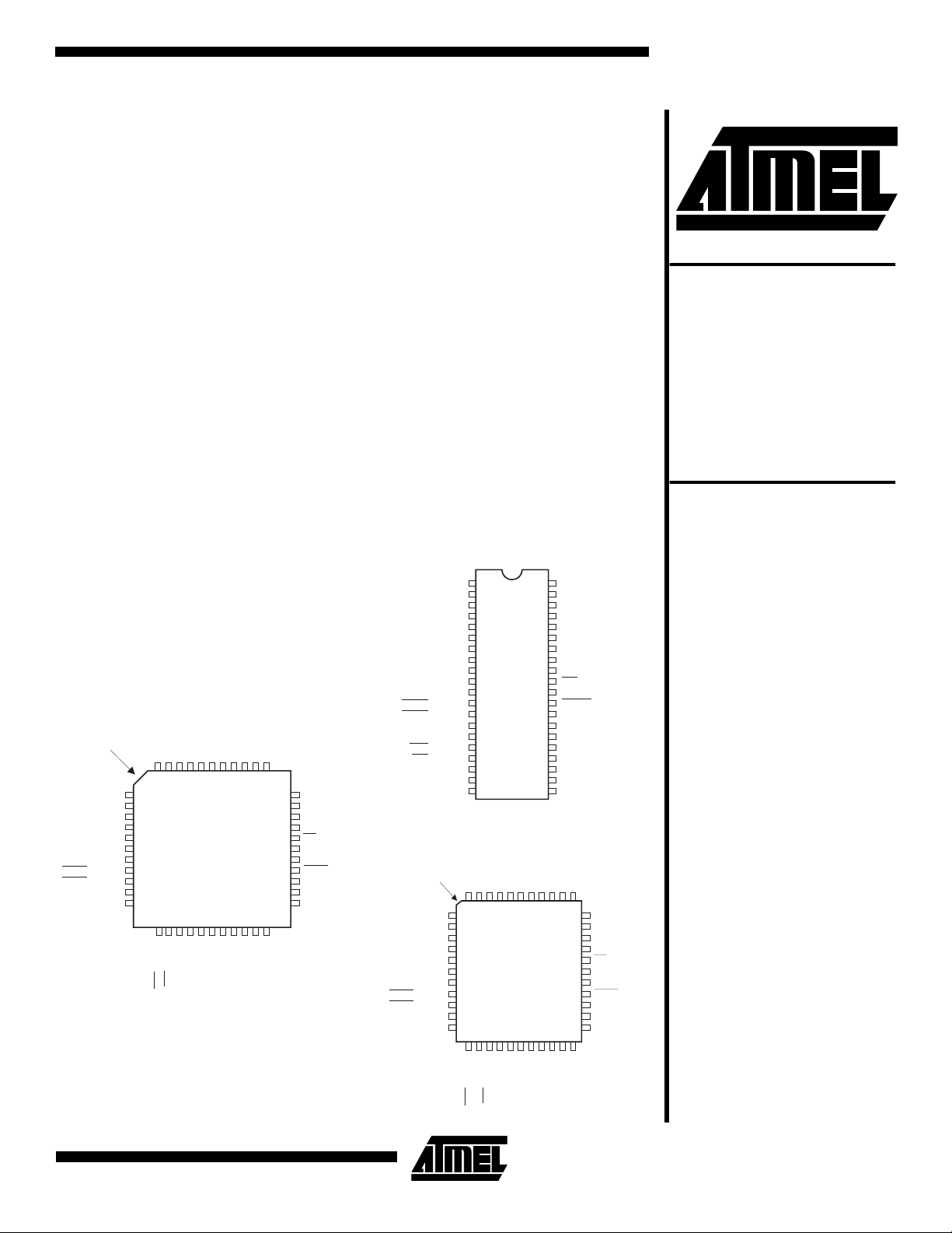
Pin Configurations
TQFP
INDEX
CORNER
P1.5
P1.6
P1.7
RST
(RXD) P3.0
(TXD) P3.1
()P3.2INT0
()P3.3INT1
(T0) P3.4
(T1) P3.5
NC
1
2
3
4
5
6
7
8
9
10
11
44
12
P1.4
13
()P3.6WR
P1.3
P1.2
424340
41
15
14
XTAL2
()P3.7RD
P1.0
P1.1
16
XTAL1
NC
39
17
GND
VCC
38
18
GND
(A8) P2.0
P0.0 (AD0)
37
19
(A9) P2.1
P0.1 (AD1)
36
20
(A10) P2.2
P0.2 (AD2)
35
21
(A11) P2.3
P0.3 (AD3)
34
22
(A12) P2.4
33
32
30
29
28
27
26
25
24
23
31
P0.4 (AD4)
P0.5 (AD5)
P0.6 (AD6)
P0.7 (AD7)
EA
NC
ALE
PSEN
P2.7 (A15)
P2.6 (A14)
P2.5 (A13)
P1.0
P1.1
P1.2
P1.3
P1.4
P1.5
P1.6
P1.7
RST
(RXD) P3.0
(TXD) P3.1
()P3.2INT0
()P3.3INT1
(T0) P3.4
(T1) P3.5
()P3.6WR
()P3.7RD P2.3 (A11)
XTAL2 P2.2 (A10)
XTAL1 P2.1 (A9)
GND P2.0 (A8)
INDEX
CORNER
P1.5
P1.6
P1.7
RST
(RXD) P3.0
NC
(TXD) P3.1
()P3.2INT0
()P3.3INT1
(T0) P3.4
(T1) P3.5
PDIP
V
1
2
3
4
5
6
7
8
9
10
11
12
13
14
15
16
17
18
19
20
40
39
38
37
36
35
34
33
32
31
30
29
28
27
26
25
24
23
22
21
P0.0 (AD0)
P0.1 (AD1)
P0.2 (AD2)
P0.3 (AD3)
P0.4 (AD4)
P0.5 (AD5)
P0.6 (AD6)
P0.7 (AD7)
EA
ALE
PSEN
P2.7 (A15)
P2.6 (A14)
P2.5 (A13)
P2.4 (A12)
PLCC
NC
VCC
P0.0 (AD0)
P0.2 (AD2)
P1.0
1
23
P0.1 (AD1)
424340
41
252827
26
P1.2
P1.1
P1.4
P1.3
65444
2
3
7
8
9
10
11
12
13
14
15
16
17 29
21
181920 24
22
CC
P0.3 (AD3)
39
38
37
36
35
34
33
32
31
30
P0.4 (AD4)
P0.5 (AD5)
P0.6 (AD6)
P0.7 (AD7)
EA
NC
ALE
PSEN
P2.7 (A15)
P2.6 (A14)
P2.5 (A13)
Microcontroller
with 4K Bytes
QuickFlash
™
Memory
AT80F51
()P3.6WR
()P3.7RD
XTAL2
XTAL1
GND
NC
(A9) P2.1
(A8) P2.0
(A10) P2.2
(A12) P2.4
(A11) P2.3
3-3
0979A-A–12/97
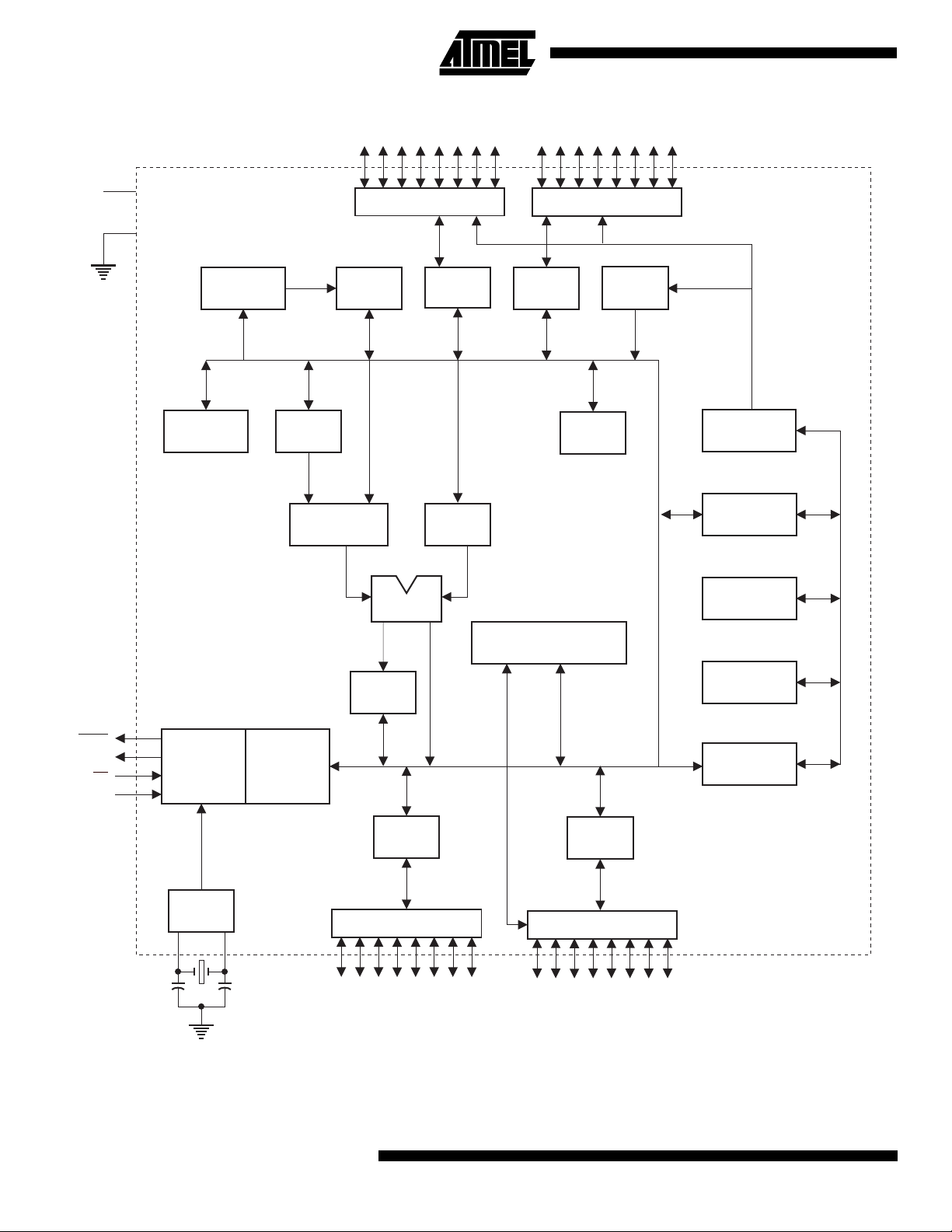
Block Diagram
V
CC
GND
RAM ADDR.
REGISTER
B
REGISTER
ACC
TMP2
P0.0 - P0.7
PORT 0 DRIVERS
RAM
PORT 0
LATCH
TMP1
PORT 2 DRIVERS
PORT 2
LATCH
POINTER
P2.0 - P2.7
QUICK
FLASH
STACK
PROGRAM
ADDRESS
REGISTER
BUFFER
PSEN
ALE
EA
RST
TIMING
AND
CONTROL
OSC
INSTRUCTION
REGISTER
ALU
PSW
PORT 1
LATCH
PORT 1 DRIVERS
P1.0 - P1.7
INTERRUPT, SERIAL PORT,
AND TIMER BLOCKS
PORT 3
LATCH
PORT 3 DRIVERS
P3.0 - P3.7
PC
INCREMENTER
PROGRAM
COUNTER
DPTR
3-4
AT80F51
AT80F51
The AT80F51 provides the following standard features: 4K
bytes of QuickFlash, 128 bytes of RAM, 32 I/O lines, two
16-bit timer/counters, a fiv e vector two-level interrup t architecture, a full duplex serial port, on-chip oscillator and clock
circuitry. In addition, the AT80F51 is designed with static
logic for operation down to zero frequency an d supports
two software select able power saving mo des. The Idle
Mode stops the CPU while allowing the RAM,
timer/counters, serial port and interrupt system to continue
functioning. The Power Down Mode saves the RAM contents but freezes the os cillato r dis ablin g all othe r chip func tions until the next hardware reset.
Pin Description
V
CC
Supply voltage.
GND
Ground.
Port 0
Port 0 is an 8-bit open drain bidirectional I/O port. As an
output port each pin can sink eight TTL inputs. When 1s
are written to port 0 pins, the pins can be used as highimpedance inputs.
Port 0 may also be configured to be the multiplexed loworder address/data bus during accesses to ex ternal program and data memory . In this m ode P0 ha s int ernal pullups.
Port 0 also out puts the c ode b yt es d uring p ro gram verification. External pu llups are requ ired dur ing pro gram ver ification.
Port 1
Port 1 is an 8-bit bidire ction al I/O por t w ith inter nal pullu ps.
The Port 1 output buffers can sink/source four TTL inputs.
When 1s are written to Port 1 pins they are pulled high by
the internal pullups and can be used as inputs. As inputs ,
Port 1 pins that are externally being pulled low will source
current (I
Port 1 also receives the low-order address bytes during
QuickFlash verification.
Port 2
Port 2 is an 8-bit bidire ction al I/O por t w ith inter nal pullu ps.
The Port 2 output buffers can sink/source four TTL inputs.
When 1s are written to Port 2 pins they are pulled high by
the internal pullups and can be used as inputs. As inputs ,
Port 2 pins that are externally being pulled low will source
current (I
Port 2 emits the high-order address byte during fetches
from external program memory and during accesses to
external data memory that use 16-bit addre sses ( MOVX @
DPTR). In this ap plication it uses strong internal pull ups
when emitting 1s. During accesses to external data mem-
) because of the internal pullups.
IL
) because of the internal pullups.
IL
ory that use 8-bit addresses (MOVX @ RI), Port 2 emits the
contents of the P2 Special Function Register.
Port 2 also receives the high-order address bits and some
control signals during QuickFlash verification.
Port 3
Port 3 is an 8-bit bidirectional I/O port with interna l pullups.
The Port 3 output buffers can sink/source four TTL inputs.
When 1s are written to Port 3 pins they are pulled high by
the internal pullups and can be used as inputs. As inputs,
Port 3 pins that are externally being pulled low will source
current (I
) because of the pullups.
IL
Port 3 also serv es t he fun ctions of v arious spe cial f eatures
of the AT80F51 as listed below:
Port Pin Alternate Functions
P3.0 RXD (serial input port)
P3.1 TXD (serial output port)
P3.2 INT0 (external in terrupt 0)
P3.3 INT1
P3.4 T0 (timer 0 external input)
P3.5 T1 (timer 1 external input)
P3.6 WR
P3.7 RD
(external interrupt 1)
(external data memory write strobe)
(external data memory read strobe)
Port 3 also receives some control signals for QuickFlash
verification.
RST
Reset input. A high on this pin for two machine cycles while
the oscillator is running resets the device.
ALE
Address Latch Enable output pulse for latching the low byte
of the address during accesses to external memory.
In normal operation ALE is emitted at a constant rate of 1/6
the oscillator fr equen cy, an d may be us ed for ex ternal timing or clocking purposes. Note, however, that one ALE
pulse is skipped during each access to external Data Memory.
If desired, ALE operation can be disabled by setting bit 0 of
SFR location 8 EH. With the bit se t, ALE is activ e only du ring a MOVX or MOVC instruction. Otherwise, the pin is
weakly pulled high. Setting the ALE-disable bit has no
effect if the microcontroller is in external execution mode.
PSEN
Program Store Enable is the read strobe to external program memory.
When the AT80F51 is executing code from external program memory, PSEN
is activated twice each machine
3-5

cycle, except that two PSEN
each access to external data memory.
EA
External Access Enable. EA must be strapped to GND in
order to enable the device to fetch code from external program memory locations starting at 0000H up to FFFFH.
Note, however, that if lock bit 1 is programmed, EA
internally latched on reset.
should be strapped to VCC for internal program execu-
EA
tions.
XTAL1
Input to the inverting os cillator ampl ifier and input to the
internal clock operating circuit.
XTAL2
Output from the inverting oscillator amplifier.
activations are skipped during
will be
Oscillator Characteristics
XTAL1 and XTAL2 are the input and output, resp ectively,
of an inverting amplifier which can be configured for use as
an on-chip oscillator, as shown in Figure 1. Either a quartz
crystal or ceramic resonator may be used. To drive the
device from an external clock source, XTAL2 should be left
unconnected while XTAL1 is driven as shown in Figure 2.
There are no requirements on the duty cycle of the external
clock signal, since the input to the internal clocking circuitry
is through a divide-by-two flip-flop, but minimum and maximum voltage high and low time specifications must be
observed.
an unexpected write to a port pin when Idle is terminated by
reset, the instruction following the one that invokes Idle
should not be one th at writes to a p ort pin or to external
memory.
Figure 1.
Note: C1, C2 = 30 pF ± 10 pF for Cry s tals
Figure 2.
Oscillator Connections
C2
XTAL2
C1
XTAL1
GND
= 40 pF ± 10 pF for Ceramic Resonators
External Clock Drive Configuration
Idle Mode
In idle mode, the CPU puts itself to sleep while all the onchip peripherals remain active. The mode is invoked by
software. The content of the on-chip RAM and all the special functions registers remain unchanged during this
mode. The idle mode can be terminated by any en abled
interrupt or by a hardware reset.
It should be noted that when idle is terminated by a hard
ware reset, the devi ce normally r esumes prog ram execution, from where it le ft off, up t o tw o machi ne c ycles befo re
the internal reset algorithm takes control. On-chip hardware
inhibits access to internal RAM in this event, but access to
the port pins is not inhibited. To eliminate the possibility of
Power Down Mode
In the power down mode the oscillator is stopped, and the
instruction that in vokes po wer down is the last instruc tion
executed. The on-chip RAM and Special Function Registers retain their values until t he power do wn mode is ter mi-
Status of External Pins During Idle and Power Down Modes
Mode Program Memory ALE PSEN PORT0 PORT1 PORT2 PORT3
Idle Internal 1 1 Data Data Data Data
Idle External 1 1 Float Data Address Data
Po w er Do wn Internal 0 0 Data Data Data Data
Power Down External 0 0 Float Data Data Data
3-6
AT80F51
 Loading...