

Features
•
Compatible with the JPEG Baseline Standard as Defined by ISO IS 109 18-1
•
Highly-integrated, Low-cost Single Chip Solution
•
Up to 40 Mbytes/sec Sustained Compression Rate
•
Maximum Processing Rate of 1.6 million pixels/sec
•
Supports 8-bit Grayscale and YUV 4:2:2 Color Space Input and Output Formats
•
Handles Images of Size up to 1024 x 1024 Pixels
•
Fast DCT/IDCT Processor On-chip
•
User-defined Quantiz atio n and Huffman Tables
•
Support for Fast as well as Slow/Inexpensive Memories
•
Provides Direct Interface for Microcontroller/Microprocessor Access
JPEG Image
Applications
The AT76C101 JPEG Processor is optimized for use in the following applications:
• Digital Cameras
• Color Printers and Plotters
• Low-cost Image Compression Systems
• Video Editing (3-4 frames/sec at CCIR 720 x 480 Image Resolution)
Hardware Resources
• On-chip Video Interface
• Custom Discrete Cosine Transform and Quantization Processor
• Variable Length and Huffman Encoder/Decoder
• Programmable Memory Interface (Supports Slow Memories)
• Microcontroller/Microprocessor Access Bus
Pin Configuration
100-Pin QFP
SRDATA
SRADDR
PXWE
PXRE
PXIN
PXOUT
STOP_PIXEL
SRDRIVE
H_SYNC
V_SYNC
PX_CLK
CLK_IN
15-0
14-0
M_ADDR
MASTER_CS
MASTER_WR
MASTER_OE
19-0
M_DATA
MEM_CS
TEST
RESET
FRAMEND
FREEZE
BUSY
BST_TEST
7-0
Compression
Processor
AT76C101
Rev. 0751A–04/98
1
Description
The AT76C101 is an Image Compression/Decompression
Processor that performs the JPEG Baseline Algorithm. The
system is cap able of h igh q uality com pres sion an d deco mpression of co ntinues -tone c olor or mono chrom e imag es.
The AT76C101 performs the Discrete Cosine Transform,
Quantization, and Entropy Encoding during the compression stage and ca rries out all inve rse operat ions during th e
decompression ph ase. The AT76C101 use s an external
SRAM as working memory, which is accessed by an onchip video interface.
The AT76C101 is designed to operate with minimum host
intervention. A host processor is required to program the
chip in the required operating mode, and to extract the
JPEG header from the compressed bit stream during the
decompression phase. Based on this information, it then
initializes the internal registers. Once the chip has been initialized, the AT76C101 operates continuously until it has
completed compression/decompression of a image frame.
The image compression ratio is contr olled by the user supplied quantization tables, which are loaded before the compression/decompression operation. Compression ratios
from 1:1 to 50:1 are possib le depe nding on the quality an d
storage requirements of the application.
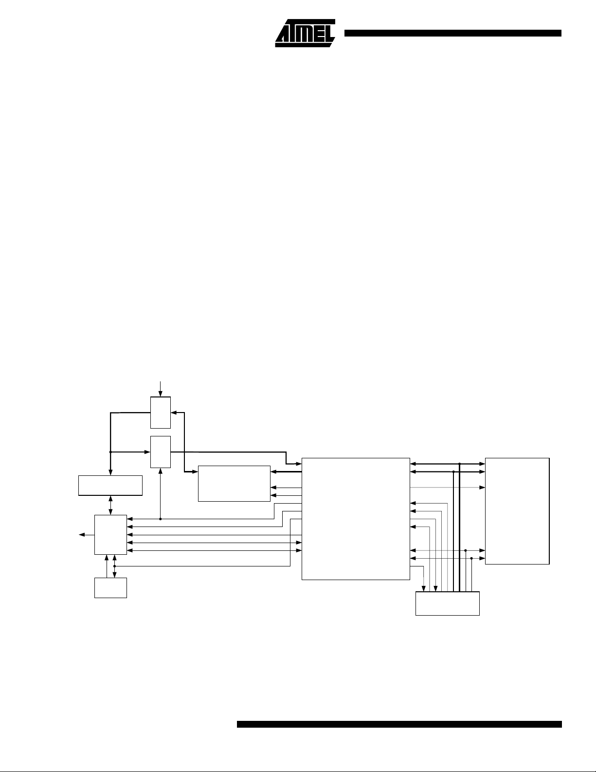
Basic System Configuration
An AT76C101-based i mage comp ression sy stem is show n
in Figure 1. The AT76C101 requires the following external
devices:
• A microcontrolle r to program and in itial ize the chip in the
required operating mode. This device is also used to
strip the JPEG header during decompression and to
provide the AT76C101 with the header information.
• An external working memory (SRAM) for handling
uncompressed/decompressed images. The size of this
memory depends on the size of the image being
processed. The formula to assess the memory size is
give n in the Pixel Interface section of this manual.
• An external memory device to store the compressed
data stream. This external memo ry can be either a fast
memory or a slow inexpensive memory. The size of this
memory depends on the needs of the specific
application.
Figure 1.
IMAGE TO
DISPLAY
AT76C101-based Image Compression System
RAW_OUT
YUV
BUFFER
OUTPUT
INPUT
BUFFER
DATA15-0 ADDR15-0
SAMPLING & COLOR
CONVERSION
RGB
VIDEO
LOGIC
INTERFACE
24-BIT
RGB
Image
Source
32K x 16
SRAM
RE
WE
SRDATA
15-0
SRADDR
14-0
PXWE
PXRE
PXIN
PXOUT
STOP_PIXEL
SRDRIVE
H_SYNC
V_SYNC
PX_CLK
CLK_IN
AT76C101
M_ADDR
19-0
M_DATA
MEM_CS
TEST
RESET
FRAMEND
FREEZE
MASTER_CS
MASTER_WR
MASTER_OE
BUSY
7-0
MICROCONTROLLER
ADDR19-0
DATA7-0
CS
COMPRESSED
DATA
MEMORY
WR
OE
2
AT76C101
System Overview
AT76C101
Pixel Interface
The pixel interface is used to input uncompressed data during the compression mode, or to output decompres sed
data during the decompression mode. The AT76C101
expects uncompresse d image d ata eithe r in YUV 4:2 :2 (for
color images), or in gray scale format. D uring decompre ssion, the AT76C101 generates images in the same format.
This interface requires an external buffer as work ing memory (Figure 2). During co mpression , the exter nal buffer is
used to store the incoming pixel s. After 8 scan lines are
read in, the AT7 6C101 perf orms a ra ster t o 8 x8 blo ck conversion of the in put data . During the invers e opera tion, th e
AT76C101 converts the outgoing pixels into the raster format and stores them in the external buffer. The uncompressed data is synchronized with the PX_CLK signal. This
clock runs at twice the pixel rate so that two transfers can
occur for each pixel, one to read pixel data from the external SRAM and one to write pixel data to the external
SRAM.
Two signals synchronize video interface operation, HSync
and VSync. These are active low, bi-directional signals and
they are controlled fr om th e Ma st er bit of th e Mo de register
of the chip. When Master is high, HSync and VS ync are
generated and driven by the chip. When Mas ter is low,
these two signa ls a re rea d a s input s by t he ch ip. In Mas ter
mode, the registers HPeriod, HSyncWidth, VPeriod, and
VSyncWidth are used to generate HSync and VSync. HPeriod contains the total number of pixels per s can line, and
HSyncWidth, the width of active HSync in number of pixels.
VPeriod and VSyncWidth provide the same type of information for VSync in terms of scan lines, rather than pixels.
These registers and others are used to control the video
interface of the chip. The other registers are HDelay, HActive, VDelay, and VActive. HDelay contains the number of
pixels between falling HSync and the first active pixel of a
line. HActive contains the number of active blocks in a line.
The size of the working memory depends on the size of the
image being processed. The external buffer should be
deep enough to store 16 scan li nes of dat a at the hi ghest
horizontal resolution. The equations for determining the
external buffer size are:
• Buffer bus width = 16 bits [For YUV data], 8 bits [For
Grayscale data]
• Buffer size = 16 x (No. of pixels per line)
As an example, a system designed to process images of
the maximum size of 1024 x 1024 pixels would have the
following external buffer requirements:
• Buffer size = 16 x 1024 = 16,384 words
Thus, this system would requ ire 1 6K x 1 6 workin g memo ry
to process YUV images (color) and 16K x 8 working memory to process grayscale images . As the minimum size of
available SRAM is 32K x 8, the SRAM requirements are as
follows: YUV/grayscale images: two 32K x 8 SRAM’s to
form a 32K x 16 SRAM.
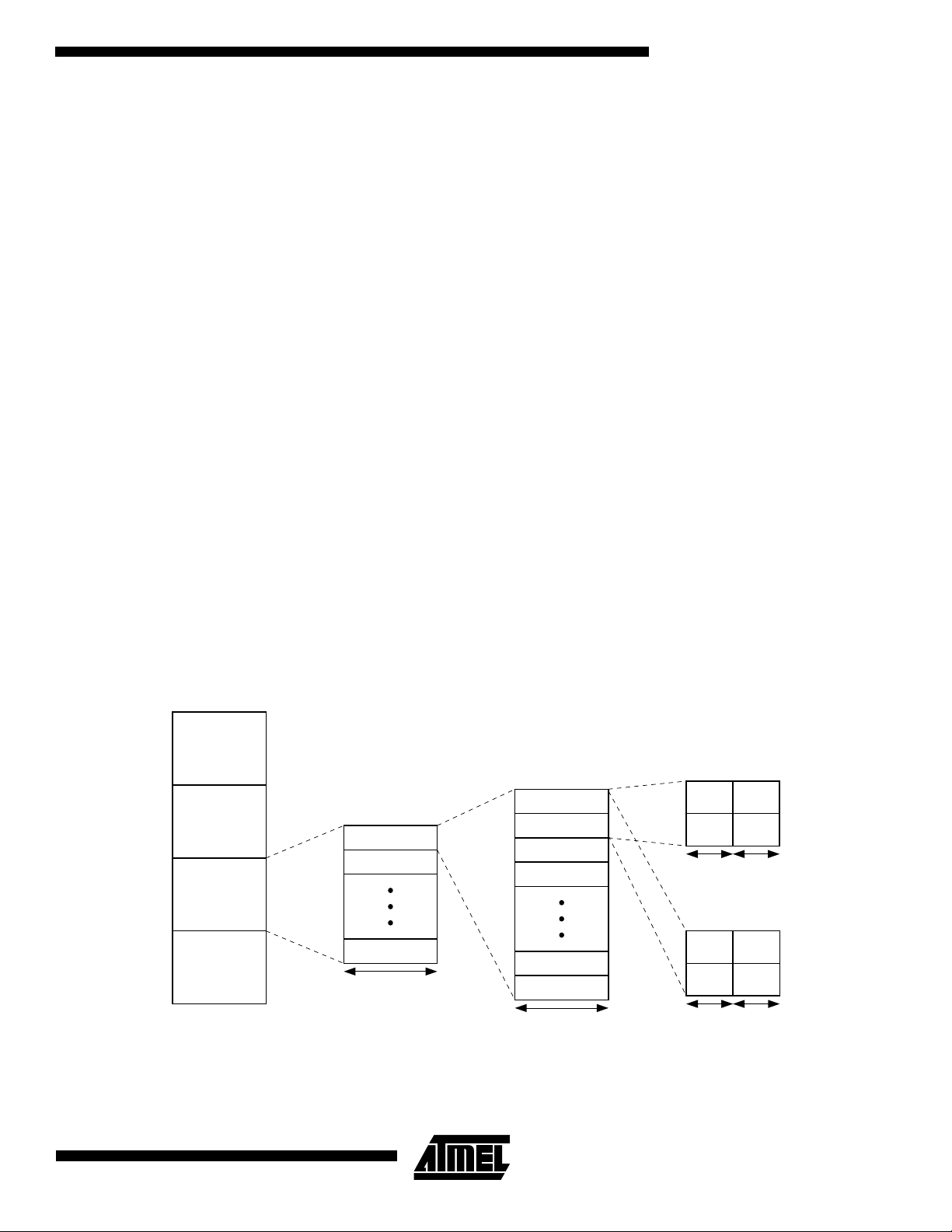
Figure 2.
Memory Organization
32K x 16 SRAM
0000h
DATABANK A
2000h
NOT USED
4000h
DATABANK B
6000h
NOT USED
7FFFh
SRAM ORGANIZATION FOR MAXIMUM SCAN LINE SIZE OF 1024 PIXELS.
EACH DATABANK STORES 8 SCAN LINES OF THE RAW IMAGE.
4000h
4400h
5C00h
DATABANK B
SCAN LINE 1
SCAN LINE 2
SCAN LINE 8
1024 PIXELS
000h
001h
002h
3FEh
3FFh
SCAN LINE
YU
YV
YU
YV
YU
YV
16 BITS
AFTER COMPRESSION
YU
YV
8 BITS
AFTER DECOMPRESSION
8 BITS
8 BITS
UY
UV
8 BITS
3
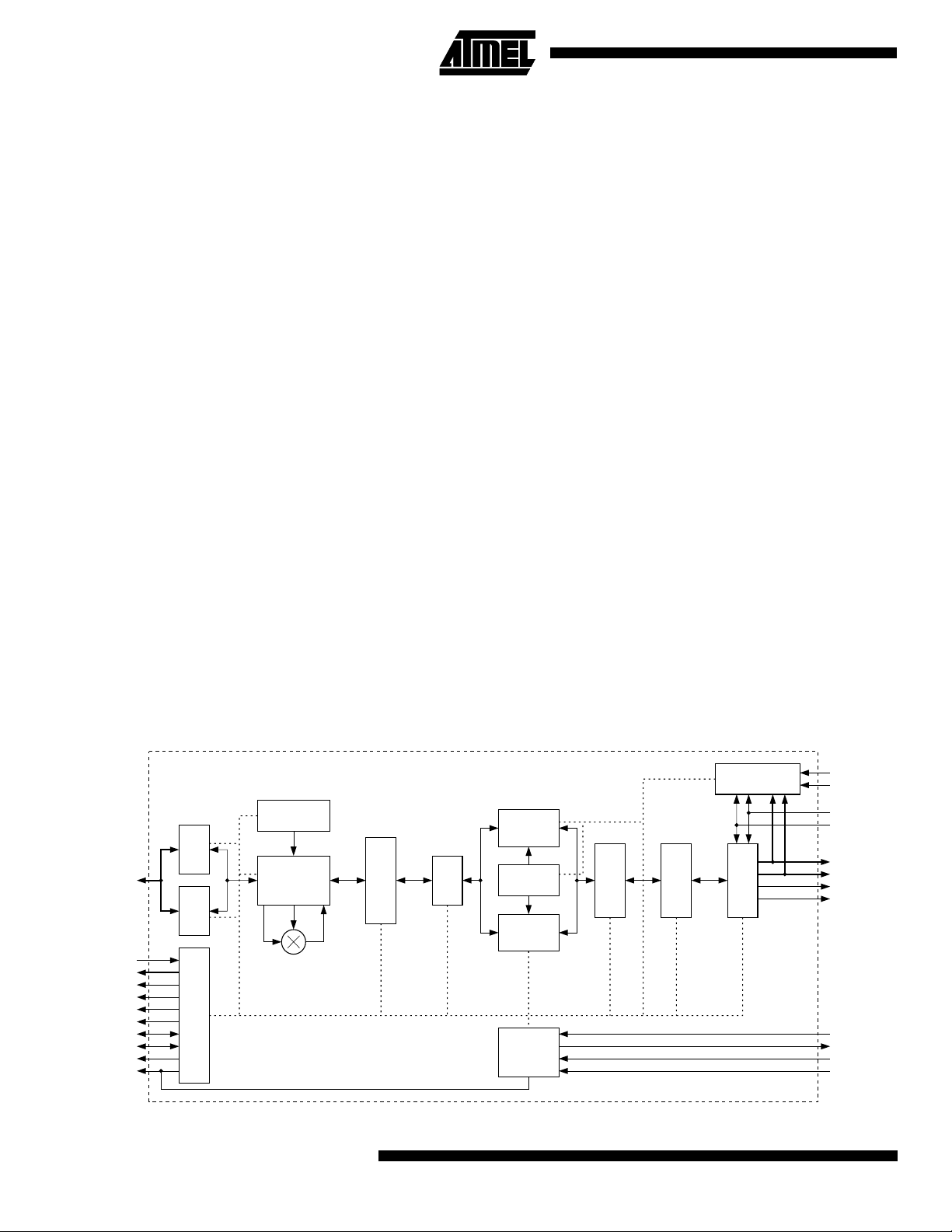
Host Interface
This is a 8-bi t i nter face that all ows t he AT76 C101 to t ran sfer the compressed data to an external memory device.
This interfaces als o allows an external micr ocontroller/microprocessor (complexity of AT89C51) to access the
internal memory (registers and tables) of the AT76C101.
Two types of transfers can be carried out through this interface: the compressed data transfers and the microcontroller data accesses.
Compressed Data Mode
The host interface can work with a number of external
memory devices. It has two programmable registers
through which the user can specify up to eight wait states
that allows the chip to inter face w ith sl ow mem ory dev ices.
Data transfers are 8 bit wide and are carried out through
the Data Bus, Address Bus and the control signals
MEM_CS, MASTER_OE and MASTER_WR. The
AT76C101 is the bu s mast er and co ntrols all tran sfers t o
the external memory. Other device s cannot access the
memory while the AT76C101 is in the operating mode.
The cycle time of the compressed data transfer varies from
one to eight CLK cycles. This cycle time is contr olled by
two registers, the Read_Cnt_Reg whi ch contro ls the read
cycle time, and Write_Cnt_Reg which controls the write
cycle time. These registers are programmed by the microcontroller during initialization. The addr ess bus is also i nitialized from the Mem _Start_A ddr reg ister, wh ich ho lds th e
start address of the compressed data memory.
Microcontroller Access Mode
In this mode, the main function of the host interface is to
allow extern al de vices , (i .e. mi croco ntrol ler or a ho st p rocessor) to access the internal memory of the JPEG chip.
This is required to program the AT76C101 in the desired
mode of operation , to load the inte rnal quantiz ation and
Huffman tables during initialization, and to read the status
of the chip for testing purposes.
All transfers to the internal memory and tables of the JPEG
codec are 8-bit wide . Data is transferr ed using the Dat a
Bus, Address Bus, and the control s ignals MASTER_WR,
MASTER_OE, MAST ER_ CS an d BUS_ BUSY. All t rans fer s
carried out in this mo de are contr olled by th e microco ntroller.
When the AT76C101 ch ip is ope ra tin g in normal mode (i.e.
either compression or decompression), it acts as a bus
master on the external memory/microcontroller bus. Since
the AT76C101 has higher priority over the micro controller
for these bus accesses, the microcontroller has to check
the availability of the bus (by check ing BU S_BU SY) bef ore
it can access it. Once all the internal registers of the
AT76C101 are set up and the tab les are loaded, the
AT76C101 is activated by setting the Start_Reg register.
Once the compression/decompression operation starts, the
AT76C101 takes control of the bus, and gives it up only
after the chip has processed the image.The microcontroller
can access the internal memo ry of the AT76C101 only
between frames and not during normal mode of operation.
Data Control
During compression, the AT76C101 monitors the internal
image buffers and s ends a stall sign al (STOP) to prevent
the external video interface logic from generating new pixels, in case the inter nal buf fers are full . Duri ng dec ompression, the AT76C10 1 controls the tran sfer rate from the
compressed data interface, based on the status of the compressed data FIFO (Figure 3).
Figure 3.
SRDATA [15:0]
PX_CLK
SRADDR [14:0]
PXRE
PXWE
PXIN
PXOUT
H_SYNC
V_SYNC
BLANK
STOP_PIXEL
4
Data Control
PIXEL
BUFFER
PIXEL
BUFFER
PIXEL
INTERFACE
QUANTIZATION
TABLE
DCT/IDCT &
QUANTIZATION
MODULE
AT76C101
BUFFER
DCT COEFFICIENT
UNIT
ZIGZAG
HUFFMAN
ENCODER
HUFFMAN
TABLES
HUFFMAN
DECODER
HIGH LEVEL
CONTROL
UNIT
BIT STUFFER
FIFO
COMP. DATA
REGISTER FILE
& TEST MODULE
HOST
INTERFACE
TEST
MASTER_CS
MASTER_OE
MASTER_WR
M_ADDR
M_DATA
MEM_CS
BUS_BUSY
RESET
END_FRAME
FREEZE
CLK_IN

AT76C101
Compressed Data Memory Management
The AT76C101 starts reading/writing data from/to the compressed data memory star ting from the ad dress location
specified by the Mem_Start_Addr register. Once a frame
has been processed, the AT76C101 writes the address of
the last compressed data into the Mem_End_Addr register.
The microcontroller uses this information to keep track of
the memory locations having va lid images , and to s pecify
the starting memory address of the next image
Initialization Sequence
The active high RESET signal resets all the AT76C101
resources including the register file. Once the AT76C101
has been reset, the microcontroller can program the chip to
the desired mode of operation. The microcontroller will also
have to load the internal Huffman and Quantization Tables.
Once the internal registers and tables have been initialized,
the microcontroller can initiate a compression/decompression operation by asserting the Start_Reg register. The
AT76C101 de-asserts this signal after the final image block
is processed. When the AT76C101 completes the processing of an image, it asse rt s th e FRA ME ND s ignal, writes the
address of the last compressed data into the
Mem_End_Addr register and waits for a new Start_Reg
request.
During decompress ion, the m icroc ontro ller h as to do s ome
additional processin g of the JP EG da ta stream. The micr ocontroller extracts and process the JPEG header information from the compres sed data stream. Based on this
header information, the micr ocontroller then initializes the
internal registers of the AT76C101 and writes the address
of the memory location containing the first compressed
image data (not the start of the JPEG header) into the
Mem_Start_Addr register. It then follows the above mentioned initialization sequence.
Quantization Table Loading
The on-chip quantization tables must be lo aded with the
required values before the normal operation of the chip.
The AT76C101’ s quan tizatio n tab le is a 256 x16 RA M, and
can store up to four 64-word quantization tables. The upper
half of the RAM area is used to store th e compression
quantization tables and the lower half to store the decompression tables. The organization of the quantization RAM
is shown in Figure 4. The Quantization Tables can be
loaded only after the Quant_Table_Load_Enable register
has been set. Once load ed, the quanti zation tabl es remain
valid until the power is switched off or until they are reprogrammed (they are unaffected by RESET). The
Quant_Table_Load_Enable register has to be reset after
the tables are loaded and before normal operation of the
chip can begin.
Figure 4.
Internal Memory Organization (Quantization and MaxMin Tables)
0000h
0000h
0002h
0080h
0100h
0180h
QUANTIZATION TABLE
3000h
3008h
3080h
3100h
3180h
Y
ENCODING
UV
Y
DECODING
UV
DC-Y
DC-UV
AC-Y
QUANTIZATION VALUE (BITS 7-0)
0001h
QUANTIZATION VALUE (BITS 15-8)
3000h
3001h
3002h
3003h
3004h
3005h
3006h
3007h
MIN_CODE (BITS 7-0)
MIN_CODE (BITS 15-8)
MAX_CODE (BITS 7-0)
MAX_CODE (BITS 15-8)
VAL_PTR
NOT USED
QUANTIZATION VALUE
16 BITS
40 BITS
VAL_PTR MAX_CODE MIN_CODE
8 BITS 16 BITS 16 BITS
AC-UV
MAXMIN TABLE
5

Before loading, the quantization tables have to be converted from the JPEG interchange format (JPEG_Q_Table)
to the AT76C101 specific format (AT76C101_Q_Table).
This format varies, based on the mode of operation of the
chip (compression or decompression). The steps to convert
to the AT76C101 specific format are given below:
• The Quantization Tables are stored in the zigzag form in
the JPEG interchange format. Convert these tables to
the normal (un-zigzagged) form.
• Convert to AT76C101 format using the following
algorithm where, M_Factor[i][j] = 16,38 4, if (i= 1 and j=1)
32,768/sqrt(2), if (i=1 and j=2.8) or (i=2.8 and j=1)
32,768 otherwise:
for (i = 1..8) begin
for (j = 1..8) begin
if (mode = COMPRESS)
AT76C101_Q_Table[i][j] =
(M_Factor[i][j]/
JPEG_Q_Table[i][j]) + 0.5
else if (mode = DECOMPRESS)
AT76C101_Q_Table[i][j] =
JPEG_Q_Table[i][j]
end
end
The Quantization tables are 16 bits wide and are loaded
using the host bus. The host bus accesses the quantization
table values in two 8-bit halves, with the lower address corresponding to the lower order byte and the higher address
corresponding to the higher order byte (Figure 4).
Huffman Table Loading
Like the Quantization tables, the AT76C101 Huffman
tables are specific to the chip. B efore normal oper ation of
the chip, the Huffman tab les must be loaded in the
AT76C101 specific format into the on-chip RAM. The
INT_Table_Load_Enable register has to be set to load the
Huffman tables. When the Huffman tables are loaded into
the internal RAM, they remain valid until the power is
switched off or until they are repr ogrammed (they are not
affected by RESET). The Huffman_Table_Load_Enable
register has to be reset after the tables are loaded and
before normal operation of the chip can begin.
The AT76C101 can store up to four Huffman tables: 2 Huffman AC tables and 2 Huffman DC tab les. The memory
organization and address mapping of the Huffman tables
are given in Figure 5. The Huffma n tables are 28 bits w ide
and consist of three fields, the si ze of the Huffman code
(stored as 1 less than actual size) , the Huffman code a nd
the 8-bit symbol corresponding to the Huffman code. Each
Huffman table value is accessed from the host bus in four
8-bit slices, with the lower order 8 bits corresponding to the
lowest address (for e.g. 2000H) and the highest 8-bit slice
(bit 24 through bit 31) corresponding to the highest address
(2003H).
Figure 5.
Internal Memory Organization (Huffman Tables)
1000h
1004h
1040h
DC HUFFMAN TABLE
2000h
2004h
2400h
AC HUFFMAN TABLE
Y
UV
Y
UV
1000h
1001h
CODE (BITS 3-0)
1002h
1003h
0000 CODE SIZE - 1 8-BIT SYMBOL
8-BIT SYMBOL
SIZE -1
CODE (BITS 11-4)
0000
CODE (BITS 15-12)
28 BITS
16 BITS 4 BITS 8 BITS
6
AT76C101

AT76C101
The Huffman tables have the same format in both the compression and decompression mode, but the arrangement of
the codes within the tables varies for the two modes. In the
compression mode , the Hu ffman t ables ar e in dexed by the
8-bit symbol corresp onding to the code. Fo r exampl e, the
luminance AC Huffman tabl e value corres pondi ng to the 8bit symbol value of 17 will be stored in the 17th location of
the table, i.e. in the address locations 4068 to 4071. In the
decompression mode, the Huffman tables are arranged in
consecutive locations in increasing order of Huffman size.
All codes of the same Huffman size are then arranged in
terms of increasing Huffm an code value. Appen dix A,
annex C of the J PEG Intern ationa l Sta ndard g ives t he procedure for generating the Huffman codes and sizes from
the Huffman tabl e information e xtracted from the compressed JPEG header.
MaxMin Table Loading
The Maxmin tables are an extra set of tables which are
required only for the decompression operation. Similar to
the Huffman tables, these tables c an be loaded o nly after
the INT_Table_ Load_Enable r egister has be en set, and
this registe r has to be r ese t be fore n orm al o perati on of th e
AT76C101 can commen ce. This table is re quired to keep
track of the maximum and minimum Huffman code values
for each Huffman code length. Since there is a maximum of
4 Huffman tables al lowed and the l onges t Huffma n co de is
16 bits wide, the r equired maxmi n tabl e size is 6 4 words .
The four maxmin tables are arranged in increasing order of
size and each word of the maxmin table is 40 bits wide with
three fields, a pointer to the position of the minimum code
of that Huffman size, the minimum Hu ffman code a nd the
maximum Huffman code corresponding to that Huffman
code size. The maxmin tables are acce ssed by the host
bus in terms of five 8-bit slices with the lowest address corresponding to bit 0-7 of the maxmin table value and the
highest address corresponding to bit 32-39 (Figure 4).
These tables are generated from the AT76C101 specific
decompression mode Huffman tables and the algorithm to
develop them is given below:
for (i = 1..16) begin
maxmin_min_code[i] = -1
maxmin_max_code[i] = -1
end
for (i=1..total_num_of_huffman_codes)
if (maxmin_min_code[size[i]] == -1)
begin
maxmin_min_code[size[i]] = code[i]
maxmin_val_ptr[size[i]] = i
end
maxmin_max_code[size[i]] = code[i]
7

Signal Description
Figure 6.
BST_TEST 57
Symbol
CLK 51
GND 52
Vcc 53
PWR 54
MAST_CS 55
TEST 56
FREEZE 58
RESET_ 59
PXWE 60
PXRE 61
PWR 62
SRADD14 63
SRADD13 64
SRADD12 65
SRADD11 66
NC 67
SRADD10 68
SRADD9 69
SRADD8 70
SRADD7 71
GND 72
SRADD6 73
SRADD5 74
SRADD4 75
GND 76
SRADD3 77
SRADD2 78
SRADD1 79
SRADD0 80
50 M_DATA7
48 GND
49 M_DATA6
46 M_DATA4
47 M_DATA5
45 M_DATA3
GND
44 M_DATA2
42
43 M_DATA1
41 M_DATA0
39 MAST_OE
40 MAST_WR
37 PWR
38 MEM_CS
35 M_ADD1
36 M_ADD0
34 M_ADD2
33 M_ADD3
32 M_ADD4
31 PWR
30 M_ADD5
29 M_ADD6
28 M_ADD7
27 M_ADD8
26 M_ADD9
25 M_ADD10
GND
24
23 M_ADD11
22 M_ADD12
21 M_ADD13
GND
20
19 M_ADD14
18 M_ADD15
17 M_ADD16
16 M_ADD17
15 M_ADD18
14 PWR
13 M_ADD19
12 BUSY
11 FRAMEND
10 stop_pixel
9 SRDRIVE
8 PWR
7 PX_CLK
6 HSync
5 VSync
4 Vcc
GND
3
2 PXOUT
1 PXIN
PWR 81
SRData15 82
8
AT76C101
PWR 85
SRData10 88
SRData12 86
SRData14 83
SRData13 84
SRData11 87
GND 91
SRData7 92
SRData8 90
SRData9 89
SRData6 93
GND 96
SRData3 97
SRData5 94
SRData4 95
SRData2 98
SRData1 99
SRData0 100

AT76C101
Table 1.
Signal Type Description
BST_TEST Input BIST test pin (used only for testing), should be grounded.
CLK Input Master Clock.
FREEZE Input Stall Signal, active high. When this signal is asserted, the chip finishes processing the current
MAST_CS Input Master Chip Select Input. Used by microcontroller to access the JPEG chip. Active low.
PX_CLK Input Video Interface Clock (27 MHz fixed).
RESET_ Input Global Reset Signal, active high, minimum pulse width is three CLK_IN 40 MHz cycles.
TEST Input Active high - Puts chip in test mode. User has access to all internal memory. Must be tied to gnd
HSync Bidirectional Indicates start of a horizontal line of the frame.
M_ADD[19:0] Bidirectional Memory/Microcontroller Address Bus. Used by JPEG chip to access the compressed data
M_DATA[7:0] Bidirectional Memory/ Microcontroller Data Bus. Used to transf er compres sed data to the e xte rnal storage unit.
MAST_OE Bidirectional Memory/ Microcontroller Read Select. Active low. Used by microcontroller to read from JPEG
MAST_WR Bidirectional Memory/Microcontroller Write Select. Active low. Used by microcontroller to write to JPEG and
Signal Description
block and then remains in that state until freeze is pulled low.
for normal operation.
memory, and used by microcontroller to access the JPEG chip.
Also used by microcontroller to program the JPEG chip.
chip and used by J PEG chip to read compressed data from memo ry.
used by JPEG to write to compressed data memory.
SRData[15:0] Bidirectional Pixel Data Bus for inputting uncompressed data in encoding mode, or for outputting
decompressed image da ta in decoding mode.
VSync Bidirectional Indicates the start of a frame.
BUSY Output Microcontroller bus busy.
Signals whether the JPEG chip (high) or microcontroller (low) controls the bus.
FRAMEND Output End of encoding/dec odi ng ope ration. FRAMEND is active after chip is re se t an d i t re ma ins a cti ve
until the Start Register is set by the host.
MEM_CS Output Compressed data memory select. Active low. Used by JPEG to select the external memor y
device used to store the compressed data stream.
PXIN Output Pixel Input Control. It is asserted low when pixels are being input from the active portion of the
frame into the strip buffer.
PXOUT Output Pixel Output Control. It ia active only when the pixels from the active region of the field are being
read from the strip buffer.
PXRE Output Active low. Controls reading data from external memory.
PXWE Output Active low. Controls writing to the external memory.
SRADD[14:0] Output Pixel Add ress Bus. This bus s pecifies the address location of the external memory device (strip
buffer), from/ to which the pixel data is transferred. Supports external memory of up to 32K
locations.
SRDRIVE Output Indicates that the AT76C101 is driving the SRDATA Bus.
stop_pixel Output When asserted, all operations in the video interface are stopped. Active when the DCT buffers
are full, or when the ext. video logic is not ready.
9

Table 2.
Register Address R/W Description
HPeriod_Low 0F800 R/W HPeriod-low byte (bit 0 to 7).
HPeriod_High 0F801 R/W HPeriod - high byte (bit 8 to 15).
HSyncWidth_Low 0F802 R/W HSyncWidth - low byte. Used only in Master mode.
HSyncWidth_High 0F803 R/W HSyncWidt h - high byte.
HDelay_Low 0F804 R/W HDelay - low byte. Delay from falling edge of HSYNC to the first active pixel.
HDelay_High 0F805 R/W HDelay - high byte.
HActive_Low 0F806 R/W HActive - low byte.
HActive_High 0F807 R/W HActive - high byte.
Register File Description
For color pictures, in Master mode, HPeriod contains one less than the number
of pixels between successive HSYNC pulses. In Slave Mode, it contains the
time between the falling edge of one HSYNC pulse and the start of the next
HSYNC pulse (in terms of pixels).
For grayscale images: set this register to 1 less than half the number of pixels
between successive Hsync pulses.
For color images: 1 less than the number of pixels that Hsync has to be held
active low.
For grayscale images: 1 less than half the number of pixels that Hsync has to
be held active low.
For color images: size of active horizontal line divided by 8.
For grayscale images: size of active horizontal line in pixels divided by 16.
VPeriod_Low 0F808 R/W VPeriod - low byte. Used in Master mode - contains the number of lines in the
frame_7.
VPeriod_High 0F809 R/W VPeriod - high byte.
VSyncWidth_Low 0F80A R/W VSyncWidth - low byte.
Used in Master mode - one less than the number of lines that Vsync has to be
held active low.
VSyncWidth_High 0F80B R/W VSyncWidth - high byte.
VDelay_Low 0F80C R/W VDelay - low byte.
VDelay_High 0F80D R/W VDelay - high byte.
VActive_Low 0F80E R/W VActive - low byte. Number of active vertical lines.
VActive_High 0F80F R/W VActive - high byte.
Start_Reg 0F810 R/W Bit 0 is used to initiate the compression/decompression pipeline.
Mode 0F812 R/W Dete rmine the device operating mode.
The function of each bi t is sho wn belo w. Bit 0: Encode(0)/Decode(1) oper ation .
Bit 1: Color(0)/Grayscale(1) Image. Bit 2: Video Master(1)/Slave(0) Mode.
Rest of bits are reserved and should be set to zero.
Int_Table_Load_Enable 0F813 R/W Various bits of this register enable loading the different tables on chip. Bit 0:
When set, enables programming the Quantization Tables. Bit 1: When set,
enables loading the Huffman Tables, including the MAXMIN tables.
Decoder_Error 0F814 R The chip sets this regis ter to 1, if an error occurs while decoding.
Decoder_Error_Code_Low 0F815 R Decoder_Error_Code - high byte.
Decoder_Error_Code_High 0F816 R Decoder_Error_Code - high byte.
10
AT76C101

AT76C101
Table 2.
Register Address R/W Description
FIFO_Status 0F817 R Sh ows the s tatus of th e inte rnal FIFO. Bit 0 is the FIFO full indicator an d bit 1 is
Write_Cnt_Reg 0F818 R/W The number of wait states required during a write to external memory is
Read_Cnt_Reg 0F819 R/W The number of wait states required during a read from external memory is
Mem_Start_Addr_Low 0F81A R/W Mem_Start_Addr - low byte. The external memor y start address is
Mem_Start_Addr_Med 0F81B R/W Mem_Start_Adrr - middle byte (bit 16 to 31)
Mem_Start_Addr_High 0F81C R/W Mem_Start_Addr - high byte (bit 32 to 39)
Mem_End_Addr_Low 0F81D R Mem_End_Addr - low byte. A T76C101 writes the address of the last byte of the
Mem_End_Addr_Med 0F81E R Mem_End_Addr - middle byte (bit 16 to 31).
Mem_End_Addr_High 0F81F R Mem_End_Addr - high byte (bit 32 to 39).
Table 3.
Module Address Range
Register File Description
the FIFO empty indicator.
programmed into this register.
programmed into this register.
programmed here.
frame written into the external memory.
Internal Memory Addressing
Quantization Tables (256 x 16 bits) 0x00000-0x001FF
DC Huffman Tables (32 x 28 bits) 0x01000-0x0107F
AC Huffman Tables (512 x 28 bits) 0x03000-0x031FF
Maxmin Tables - For Decoding only (64 x 40 bits) 0x04000-0x04200
Pixel Buffer (4 buffers of size 128 x 8 bits each) 0x04000-0x04200
DCT Coefficient Buffer (2 buffers of size 64 x 16 each) 0x05000-0x050FF
Compressed Data FIFO (64 x 8 bits) Write Port 0x06000-0x06040
Read Port 0x07000-0x07040
11

Table 4.
AC Characteristics
Symbol Parameter Min Max Units
t
CSS
t
AS
t
AH
t
DS
t
DH
t
WPL
t
WREC
t
ACC
t
RPL
t
RREC
t
CYC
Chip Select Setup Time 3 ns
Address Setup Time 3 ns
Address Hold Time 0 ns
Data Setup Time 3 ns
Data Hold Time 0 ns
Write Pulse Width 75 ns
Write Recovery Time 125 ns
Read Access Time 120 ns
Read Pulse Length 120 ns
Read Recovery Time 50 ns
Compressed Memory
1 8 CLK_IN Cycles
Read/Write Cycle Time
t
SWR
t
SOE
Figure 7.
ADDRESS
DATA
MEMCS
MAST_WR
Figure 8.
ADDRESS
DATA
MEMCS
MAST_OE
Compressed Memory
Write Set-up Time
Compressed Memory
Read Set-up Time
Compressed Memory Write
ADDRESS VALID
DATA VALID
tSWR
tCYC
Compressed Memory Read
ADDRESS VALID
DATA INVALID
tSOE
tCYC
DATA VALID
0.5
0.5
Figure 9.
MASTER_WR
MASTER_CS
Figure 10.
MASTER_OE
MASTER_CS
Microcontroller Wr it e
M_ADDR
M_DATA
ADDRESS VALID
tCSS
Microcontroller Read
M_ADDR
M_DATA
ADDRESS VALID
tCSS
tAHtAS
tAHtAS
tACC
VALID
DATA VALID
tDHtDS
tWREC
tWPL
DATA VALID
tRREC
tRPL
12
AT76C101

AT76C101
Electrical Specifications
Table 5.
Symbol Parameter Min Max Unit Conditions
V
V
V
o
+-I
Absolute Maximum Ratings
cc
i
Ik
DC supply voltage -0.3 4.6 V Core and standard IOS
DC input voltage -0.3 Vdd + 0.3V V or see +-IIk
DC output voltage Vdd + 0.3V V or see +-IOk
DC input diode current 10 mA Vi<-0.5V
Vi>Vdd+0.5V
+-I
OK
DC output diode current 10 mA V0<-0.5V
V0>Vdd+0.5V
I
olMAX
I
ohMAX
t
SH
T
A
T
SG
Table 6.
Continuous output current 10 mA Industrial
Continuous output current 10 mA Industrial
Time of outputs shorted 5 sec
Temperature range -40 +85 C Industrial
Storage Temperature -65 +150 C
Recommended Operating Conditions
Symbol Parameter Min Typ Max Unit Conditions
V
cc
V
i
V
0
T
A
T
R
T
F
DC supply voltage 3 3.3 3.6 V
DC input voltage 0 Vdd V
DC output volta ge 0 Vdd V
Temperature range -40 +85 C Industrial
Input rise time 15 ns 10%-90% CMOS
Input fall time 15 ns 10%-90% CMOS
Table 7.
DC Characteristics
Symbol Para mete r
I
ih
I
il
I
oz
Input leakage, no pullup
Input leakage, no pullup
High-impedance outpu t current
bi-directional pins
V
il
V
ih
V
OL
V
OH
C
IN
Low level input voltage
High level input voltage
Low level input voltage
High level input voltage
Input capacitance pF
Min Max Unit
µA
µA
µA Vcc = 5.5V
V
V
V
V
Conditions
Vin = Vcc = 5.5V
Vin = 0, Vcc = 5.5V
CMOS input s and bi-dir.
CMOS input s and bi-dir.
IOL = 5.0mA
I
= 5.0mA
OH
13
 Loading...