

ATMEL AT76C001 Datasheet

CBIC
Programmable
FIR Filter
AT76C001
Features
4 Multiplier-Accum ul ators
•
40 Bits Accuracy
•
16 Bit Data and Coefficients
•
4-tap Filter With 27 MHz Sample Rate
•
Programmable to Give up to 256 Tap s With Sampling
•
Reducing Propo rtionally to 421,875 kHz
Programmable Round ing and Truncation to 16 Bit
•
8 Bit Standard Microprocess or In terfa ce
•
64-pin PQFP, 68-pin PGA68 or 68-pi n LCC6 8 Pac ka gi ng
•
Description
The AT76C001 Programmable Finite Impulse Response (FIR) Filter implements a
4th order FIR cell built around 4 multiplier-accumulators. It contains a dual-port
RAM and a RAM which are used to implement FIR filters of up to 256 taps. High order filters are achieved by multiplexing the 4th order cell and accumulating the intermediate results up to 40 bits, so that there is no loss of accuracy.
The maximum frequency of the AT76C001 is 27 MHz. For 4-tap FIR filter, the incoming sample rate can be as high as 27 MHz. For higher order FIR filters, the
sample rate can be as high as the circuit frequency divided by the 4th order cell multiplexing factor.
A programmable normalization block allows the choice of the 16 significant bits from
the 40 bit internal result which can be previously rounded by adding 0.5 LSB according to the 16 significant bit locations. The AT76C001 has a microprocessor interface which can be configured to be Intel or Motorola compatible.
Applications
Digital Filters (vi de o, aud io, etc.)
•
Correlation
•
Image Processi ng
•
AT76C001
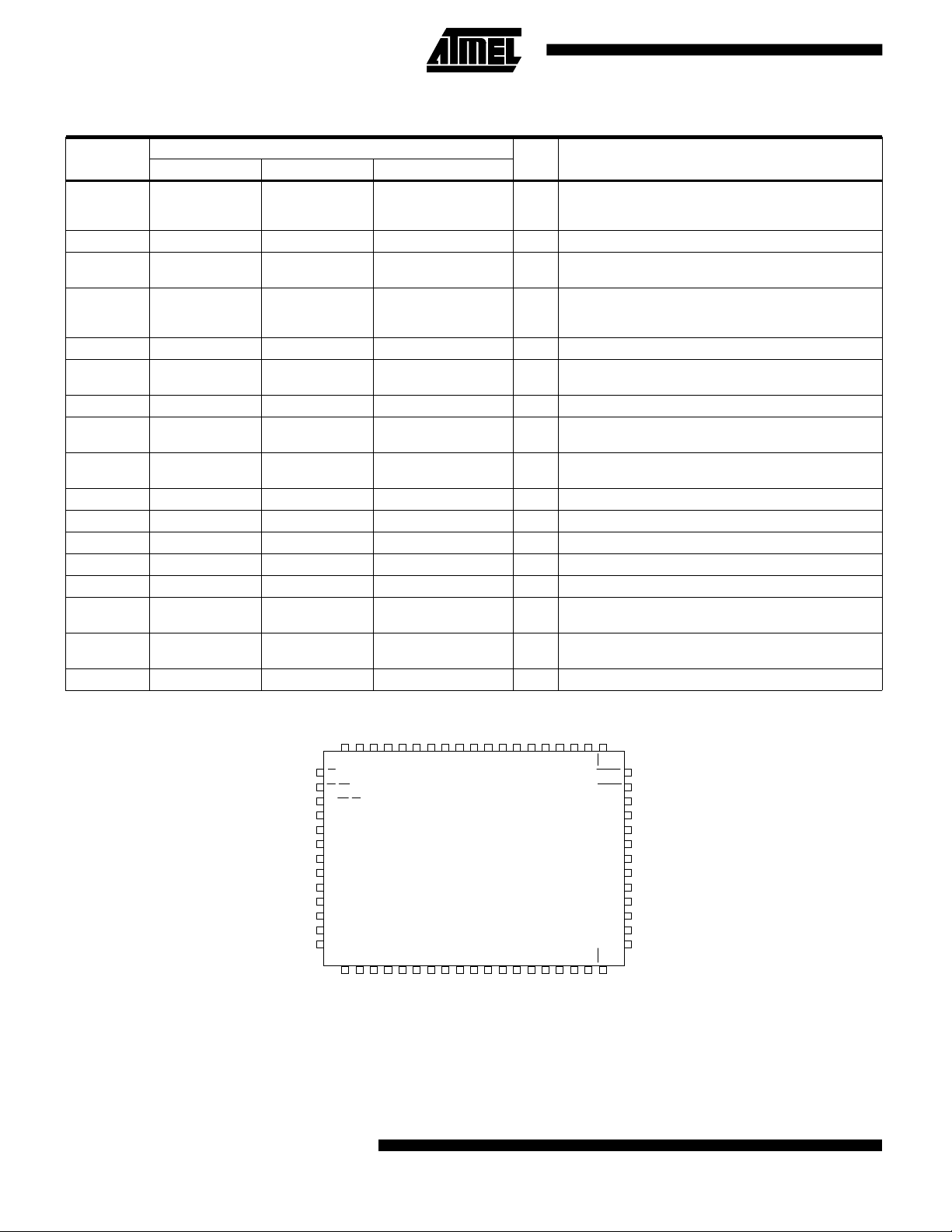
Pin Description
Name
Pin Number
Type Function
QFP64 Packaging LCC68 Packaging PGA68 Packaging
K10-11, J10-11, H10-
IN<15:0> 34-40, 42, 44-51 27-33, 35, 37-44
11, G10, F10, E10-11,
I Input sample
D10-11, C10-11, B11-10
DIV 33 26 L10 I Input sample valid. Active low
RST_X1 32 24 K9 I
Force input sample to 0. Useful for interpolation
implementation
K1, J1-2, H1-2, G1-2,
OUT<15:0> 18-12, 10, 8-1 9-3, 1, 67-60
F2, E2, D1-2, C1-2, B1-
O Output filtered sample
2, A2
DOV 19 10 K2 O Output filtered sample valid. Activ e low
DATA<7:0> 21-24, 26, 28-30 13-16, 18, 20-22 L3, K4, L4, K5-7, L7, K8 I/O
Microprocessor interface data bus. Used for accessing
internal registers and to write the coeffic i ents of the filt er
CS 52 46 B9 I Chip select. Active low
DS/WR 53 47 A9 I
RDWR/RD 54 48 B8 I
Microprocessor interface data strobe (Motorola mode) or
Write signal (Intel mode). Active low
Microprocessor interface Read/Write signal (Motorola
mode) or Read signal (Intel mode). Active low
ADD<1:0> 63-64 57-58 A4, B3 I Microprocessor interface address bus
RESET 31 23 L8 I Circuit master reset. Active low
CLOCK 56 50 B7 I Circuit clock (27 MHz max)
CLOCK_BIST 61 55 A5 I For internal use. Connect to ground
TEST_BIST 20 12 K3 I For internal use. Connect to ground
VCC
GND
11, 27, 43, 58, 60,622, 19, 36, 52, 54,
56
9, 25, 41, 55, 57,
59
17, 34, 49, 51, 53 A6-8, E1, G11, L5 Ground
B4-6, F1, F11, L6 Power supply (+5V)
NC 11, 25, 45, 59 A3, A10, L2, L9 No connection
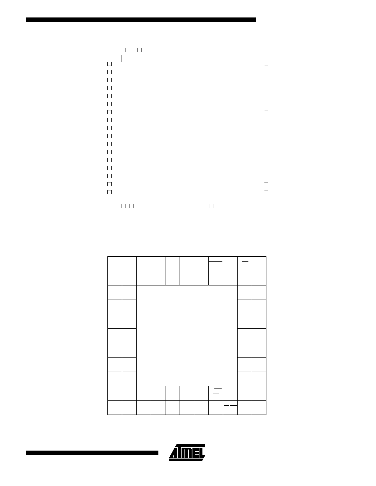
51 50 49 48 47 46 45 44 43 42 41 40 39 38 37 36 35 34 33
IN0
52
CS
53
DS/WR
54
RDWR/RD
55
GND
56
CLOCK
57
GND
58
VCC
59
GND
60
VCC
61
CLOCK_BIST(0)
62
VCC
63
ADD1
ADD
64
0
OUT0
(0): Connect to GND
12345678910111213141516171819
Plan View of AT76C001 in QFP64 Package
2 AT76C001
IN5
IN1
IN2
OUT1
OUT2
IN6
IN3
IN4
IN7
AT76C001
OUT3
OUT4
OUT5
OUT6
OUT7
IN8
VCC
QFP64
OUT8
GND
IN9
GND
IN10
IN11
IN12
OUT11
OUT10
OUT12
OUT9
VCC
DIV
IN13
IN14
IN15
RST-XI
32
RESET
31
DATA0
30
DATA1
29
DATA2
28
VCC
27
DATA3
26
GND
25
DATA4
24
DATA5
23
DATA6
22
DATA7
21
TEST_
20
BIST
OUT13
(0)
OUT14
OUT15
DOV
AT76C001
25 24 23 22 21 20 19 18 17 16 15 14 13
26
27 IN15
28
29
30
31
32
33
34
35
36
37
38
39
40
41
42
43
(0): Connect to GND
DIV
IN14
IN13
IN12
IN11
IN10
IN9
GND
IN8
VCC
IN7
IN6
IN5
IN4
IN3
IN2
IN1
IN0
44
45 46 47 48 49 50 51 52 53 54 55 56 57
NC*
DATA0
RESET
RST_XI
VCC
GND
DATA1
DATA2
DATA4
DATA3
DATA7
DATA5
DATA6
AT76C001
LCC68
NC*
CS
GND
RDWR/RD
CLOCK
VCC
VCC
GND
GND
VCC
CLOCK_BIST(0)
ADD1
DS/WR
Plan view of AT76C001 in LCC68 package
12
58
11 10
TEST_BIST(0)
ADD0
59 60
NC*
DOV
OUT15
OUT14
OUT13
OUT12
OUT11
OUT10
OUT9
VCC
OUT8
GND
OUT7
OUT6
OUT5
OUT4
OUT3
OUT2
OUT1
NC*
OUT0
* No Connection
9
8
7
6
5
4
3
2
1
68
67
66
65
64
63
62
61
1234567891011
L NC* DATA7 DATA5 GND VCC DATA1 RESET NC*
OUT15 DOV TC(0) DATA6 DATA4 DATA3 DATA2 DATA0 RST_XI
K
OUT14 OUT13
J
OUT12 OUT11
H
OUT10 OUT9
G
VCC OUT8
F
GND OUT7
E
OUT6 OUT5
D
OUT4 OUT3 IN3 IN2
C
OUT2 OUT1 ADD0 VCC VCC VCC CLOCK
B
A
OUT0 NC* ADD1 CB(0) GND GND GND DS/WR
AT76C001
PGA68
RDWR/
RD
(0): Connect to GND
DIV
IN15 IN14
IN13 IN12
IN11 IN10
IN9 GND
IN8 VCC
IN7 IN6
IN5 IN4
CS
IN0 IN1
NC*
* No Connection
Plan view of AT76C001 in PGA68 packa ge
3
 Loading...