


查询AT75C221供应商查询AT75C221供应商
Features
•
ARM7TDMI® ARM® Thumb® Processor Core
– In-Circuit Emulator, 40 MHz operation
•
16-bit Fixed-point OakDSPCore®
– Up to 60 MHz operations
– 104K bytes of Integrated Fast RAM, Codec Interface
•
Ethernet Bridge
– Dual Ethernet 10/100 Mbps MAC Interface
– 16-Kbyte Frame Buffer
•
1 K-Byte Boot ROM, Embedding a Boot Program
– Enable Application Download from DataFlash
•
External Bus Interface
– On-chip 32-bit SDRAM Controller
– 4 Chip Select Static Memory Controller
•
Multi-level Priority, Individually Maskable, Vectored Interrupt Controller
•
Three 16-bit Timer/Counters
•
Two UARTs with Modem Control Lines
•
Serial Peripheral Interfa ce (SPI)
•
Two PIO Controllers, Managing up to 48 General-purpose I/O Pins
•
Supported by a Wide Range of Ready-to-use Application Software
– Multi-tasking Operating System, Networking
– Voice-processing Functions
•
Available in a 208-lead PQFP Package and 256-ball BGA Package
•
Power Supplies
– VDDIO 3.3V nominal
– VDDCORE and VDDOSC 1.8V nominal
•
0°C to + 70°C Operating Temperature Range
®
Smart Internet
Appliance
Processor
(SIAP™)
AT75C221
Summary
Description
The AT75C221, Atmel’s latest device in the family of smart internet appliance p roce ssors (SIAP
appliance appl icatio ns such as the Et her net IP phone. Th e AT75C221 is built aroun d
an ARM7TDMI microcontroller core running at 40 MHz with an OakDSPCore coprocessor running at 60 MHz and a dual Ethernet 10/100 Mbits/sec MAC interface.
In a typical standalone IP phone, the DSP handles the voice processing functions
(voice compression, acoustic echo cancellation, etc.) while the dual-por t Ether net
10/100 Mbits/sec MAC interface establishes the connection to the Ethernet physical
layer (PHY) that links the network and the PC. In such an application, the power of the
ARM7TDMI allows it to run a VoIP protocol stack as well as all the system control
tasks.
Atmel provides the A T75C221 with several software modules, including:
• A set of drivers for a Linux
• A comprehensive set of tuna ble DSP algorithms for voice processing, tailored to
be run by the DSP subsystem.
™
), is a high-performance processor de signed for professional inter net
®
kernel capable of driving the embedded peripherals.
6033CS–INTAP–05/04

Pinout
The AT75C221 ships in two alternative packages:
• 208-lead PQFP
• 256-ball BGA
The product feature s of the 25 6-bal l BG A pack age ar e incre ased com pared to the 2 08-
lead PQFP package.
The features available only with the BGA pac kage ar e:
• The 32-bit wide data bus (In PQFP, only a 16-bit wide data bus is supported.)
• The Parallel I/O lines PA13 to PA18 and PA20 to PA31
• The Parallel I/O lines PB10 to PB16
2
AT75C221 Summary
6033CS–INTAP–05/04

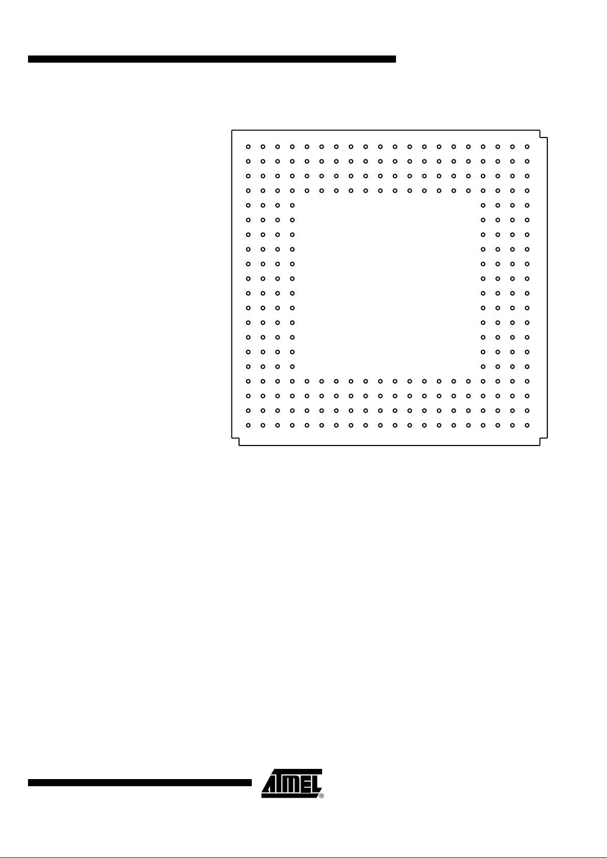
208-lead PQFP Package Pinout
AT75C221 Summary
Table 1.
Pin
Number Signal Name
1 GND 37 MB_TXD0 73 A15 109 RAS
2 SCLKA 38 MB_TXD1 74 A16 110 CAS
3 VDDIO 39 MB_TXD2 75 A17 111 NC
4 FSA 40 GND 76 A18 112 WE
5 STXA 41 MB_TXD3 77 A19B/A0 113 DQM0
6 SRXA 42 MB_TXEN 78 A20/BA1 114 DQM1
7 NTRST 43 MB_TXCLK 79 A21 115 NC
8 MA_COL 44 MB_RXD0 80 D0 116 GND
9 MA_CRS 45 MB_RXD1 81 D1 117 NC
10 MA_TXER 46 MB_RXD2 82 D2 118 VDDCORE
11 MA_TXD0 47 MB_RXD3 83 D3 119 GND
12 MA_TXD1 48 MB_RXER 84 GND 120 VDDOSC
13 MA_TXD2 49 MB_RXCLK 85 D4 121 PLLRC
14 MA_TXD3 50 MB_RXDV 86 VDDIO 122 GND
15 MA_TXEN 51 MB_MDC 87 D5 123 GND
16 VDDIO 52 VDDIO 88 D6 124 XTALOUT
17 MA_TXCLK 53 GND 89 D7 125 XTALIN
18 GND 54 MB_MDIO 90 D8 126 VDDCORE
19 MA_RXD0 55 MB_LINK 91 D9 127 NCE0
20 MA_RXD1 56 A0 92 D10 128 NCE1
21 MA_RXD2 57 A1 93 D11 129 NCE2
22 MA_RXD3 58 A2 94 D12 130 VDDIO
23 MA_RXER 59 A3 95 D13 131 NCE3
24 MA_RXCLK 60 A4 96 D14 132 NWE0
25 GND 61 A5 97 VDDCORE 133 NWE1
26 VDDCORE 62 A6 98 GND 134 NC
27 MA_RXDV 63 A7 99 D15 135 VDDIO
28 MA_MDC 64 A8 100 VDDIO 136 GND
29 MA_MDIO 65 A9 101 GND 137 NC
30 MA_LINK 66 A10 102 VDDIO 138 NWR
31 MB_COL 67 A11 103 NC
32 MB_CRS 68 A12 104 VDDIO 140 GND
33 GND 69 VDDIO 105 GND 141 VDDCORE
34 VDDCORE 70 GND 106 SDCK 142 VDDIO
35 VDDIO 71 A13 107 SDCS 143 MISO
36 MB_TXER 72 A14 108 SDA10 144 MOSI
Pinout for 208-lead PQFP Package
Pin
Number Signal Name
Pin
Number Signal Name
(1)
Pin
Number Signal Name
(1)
(1)
(1)
(1)
(1)
139 NSOE
6033CS–INTAP–05/04
3
Table 1.
Pinout for 208-lead PQFP Package (Continued)
Pin
Number Signal Name
145 SPCK 161 TMS 177 PA5 193 GND
146 PA22 162 TCK 178 PA4 194 PB0
147 VDDIO 163 PA19 179 PA3 195 PB1
148 GND 164 VDDCORE 180 PA2 196 PB2
149 NRST 165 GND 181 PA1 197 PB3
150 FIQ 166 PA12 182 PA0 198 PB4
151 IRQ0 167 GND 183 GND 199 PB5
152 TST 168 VDDIO 184 RXDA 200 PB6
153 GND 169 PA11 185 TXDA 201 PB7
154 VDDCORE 170 PA10 186 NRSTA 202 PB8
155 NC
156 VDDIO 172 PA8 188 NDTRA 204 VDDIO
157 GND 173 PA7 189 NDSRA 205 DBW32
158 VDDIO 174 PA6 190 NDCDA 206 GND
159 TDO 175 VDDIO 191 RXDB 207 BO256
160 TDI 176 NC
(1)
Pin
Number Signal Name
171 PA9 187 NCTSA 203 PB9
(1)
Pin
Number Signal Name
192 TXDB 208 VDDIO
Pin
Number Signal Name
Note: 1. NC pins should be left unconnected.
Figure 1.
208-lead PQFP Package Orientation (Top View)
105156
157
208
152
104
53
4
AT75C221 Summary
6033CS–INTAP–05/04

256-ball BGA Package Pinout
AT75C221 Summary
Table 1.
Pinout for 256-ball BGA Package
Pin Signal Name Pin Signal Name Pin Signal Name Pin Signal Name
A1 GND B18 TDI D15 VDDIO H20 NSOE
A2 PB9 B19 NC
A3 PB4 B20 NC
(1)
(1)
D16 PA24 J1 MA_TXEN
D17 GND J2 MA_TXD3
A4 PB1 C1 PB10 D18 PA29 J3 MA_TXD2
A5 NDSRB C2 PA28 D19 VDDCORE J4 MA_TXD1
A6 NRSTB C3 DBW32 D20 IRQ1 J17 NWR
A7 RXDB C4 PB6 E1 STXA J18 NWE3
A8 NDSRA C5 PB2 E2 FSA J19 NC
(1)
A9 TXDA C6 NRIB E3 SCLKA J20 NWE2
A10 PA2 C7 NCTSB E4 PA25 K1 MA_RXD0
A11 PA3 C8 NRIA E17 PA30 K2 MA_TXCLK
A12 PA6 C9 NCTSA E18 TST K3 NC
(1)
A13 PA10 C10 PA0 E19 IRQ0 K4 VDDIO
A14 PA13 C11 PA4 E20 NC
(1)
K17 NWE1
A15 PA15 C12 PA8 F1 PB13 K18 NWE0
A16 PA19 C13 PA12 F2 PB12 K19 NCE3
A17 NC
(1)
C14 PA14 F3 SRXA K20 NCE2
A18 PA23 C15 PA18 F4 VDDIO L1 MA_RXD1
A19 TDO C16 PA21 F17 VDDIO L2 MA_RXD2
A20 NC
B1 BO256 C18 NC
B2 PB8 C19 NC
(1)
C17 TCK F18 FIQ L3 MA_RXD3
(1)
(1)
F19 NC
F20 SPCK L17 VDDIO
(1)
L4 MA_RXER
B3 PB7 C20 PA31 G1 MA_COL L18 NCE0
B4 PB3 D1 PB11 G2 PB15 L19 NC
(1)
B5 PB0 D2 PA27 G3 PB14 L20 NCE1
B6 NDTRB D3 PA26 G4 NTRST M1 MA_RXCLK
B7 TXDB D4 GND G17 NRST M2 VDDCORE
B8 NDCDA D5 PB5 G18 PA22 M3 MA_RXDV
B9 NRSTA D6 VDDIO G19 MOSI M4 MA_MDC
B10 PA1 D7 NDCDB G20 MISO M17 PLLRC
B11 PA5 D8 GND H1 MA_TXD0 M18 NC
(1)
B12 PA7 D9 NDTRA H2 MA_TXER M19 XTALOUT
B13 PA11 D10 RXDA H3 MA_CRS M20 XTALIN
B14 VDDCORE D11 VDDIO H4 GND N1 MA_MDIO
B15 PA16 D12 PA9 H17 GND N2 MA_LINK
B16 PA20 D13 GND H18 VDDIO N3 MB_COL
B17 TMS D14 PA17 H19 VDDCORE N4 GND
6033CS–INTAP–05/04
5

Table 1.
Pinout for 256-ball BGA Package (Continued)
Pin Signal Na m e Pin Signal Name Pin S ignal Name Pin Signal Name
N17 GND T20 SDCS V7 A11 W14 D12
N18 DQM3 U1 MB_RXD0 V8 A14 W15 VDDCORE
N19 VDDCORE U2 MB_RXD2 V9 A18 W16 D17
N20 VDDOSC U3 MB_RXCLK V10 A22 W17 D20
P1 MB_CRS U4 GND V11 D2 W18 D24
P2 VDDCORE U5 A1 V12 D6 W19 VDDIO
P3 MB_TXD0 U6 VDDIO V13 D10 W20 NC
P4 MB_TXD3 U7 A8 V14 D14 Y1 NC
P17 RAS U8 GND V15 NC
(1)
Y2 MB_MDIO
(1)
(1)
P18 DQM0 U9 A17 V16 D19 Y3 A2
P19 DQM1 U10 VDDIO V17 D23 Y4 A3
P20 DQM2 U11 D3 V18 D26 Y5 A6
R1 MB_TXER U12 D7 V19 NC
(1)
Y6 A10
R2 MB_TXD1 U13 GND V20 D29 Y7 A13
R3 MB_TXEN U14 D16 W1 MB_MDC Y8 A16
R4 VDDIO U15 VDDIO W2 NC
R17 VDDIO U16 D22 W3 NC
(1)
(1)
Y9 A20/BA1
Y10 A23
R18 SDA10 U17 GND W4 MB_LINK Y11 D0
R19 CAS U18 D27 W5 A5 Y12 D4
R20 WE U19 NC
(1)
W6 A9 Y13 D8
T1 MB_TXD2 U20 D30 W7 A12 Y14 D11
T2 MB_TXCLK V1 MB_RXD3 W8 A15 Y15 D13
T3 MB_RXD1 V2 MB_RXDV W9 A19/BA0 Y16 D15
T4 MB_RXER V3 NC
(1)
W10 A21 Y17 D18
T17 D28 V4 A0 W11 D1 Y18 D21
T18 D31 V5 A4 W12 D5 Y19 D25
T19 SDCK V6 A7 W13 D9 Y20 NC
(1)
Note: 1. NC Balls should be left unconnected.
6
AT75C221 Summary
6033CS–INTAP–05/04
AT75C221 Summary
Figure 2.
A
B
C
D
E
F
G
H
J
K
L
M
N
P
R
T
U
V
W
Y
256-ball Package Orientation (Top View)
1
2
3
4
5
6
7
8
9
1011121314151617181920
6033CS–INTAP–05/04
7

Signal Description
Table 1.
Block Signal Name Function Type
Power Supplies
External Bus Interface
Synchronous Dynamic
Memory Controller
Static Memory Controller
Signal Description
VDDIO I/O Lines Power Supply
VDDCORE Device Core Power Supply
VDDOSC PLL and Oscillator Power Supply
GND Ground
A0-A23 Address Bus Output
D0-D31 Data Bus Input/Output
SDCK SDRAM Clock Output
DQM0-DQM3 SDRAM Byte Masks Output
SDCS SDRAM Chip Select Output
SDA10 SDRAM Address Line 10 Output
RAS Row Address Strobes Output
CAS Column Address Strobes Output
WE Write Enable Output
BA0-BA1 Bank Address Line Output
NCE0-NCE3 Chip Selects Output
NWE0-NWE3 Byte Select/Write Enable Output
NSOE Output Enable Output
NWR Memory Block Write Enable Output
PIO Controller A PA0-PA31 PIO Controller A I/O Lines Input/Output
PIO Controller B PB0-PB15 PIO Controller B I/O Lines Input/Output
TCLK0-TC LK2 Timer Counter Clock 0 to 2 Input
Timer Counter
Serial Peripheral Interface
TIOA0-TIOA2 Timer Counter I/O Line A 0 to 2 Input/Output
TIOB0-TIOA2 Timer Counter I/O Line B 0 to 2 Input/Output
MISO Master In/Slave Out Input/Output
MOSI Master Out/Slave In Input/Output
SPCK Serial Clock Input/Output
NPCS0/NSS Peripheral Chip Select 0/Slave Select Input/Output
NPCS1-NPCS3 Peripheral Chip Select 1 to 3 Output
8
AT75C221 Summary
6033CS–INTAP–05/04

AT75C221 Summary
Table 1.
Block Signal Name Function Type
UART A and UART B
MAC A Interface
Signal Description (Contin ued )
RXDA-RXDB Receive Data Input
TXDA-TXDB Transmit Data Output
NRTSA-NRSTB Ready to Send Output
NCTSA-NCTSB Clear to Send Input
NDTRA-NDTRB Data Terminal Ready Output
NDSRA-NDSRB Data Set Ready Input
NDCDA-NDCDB Data Carrier Detect Input
NRIA-NRIB
MA_COL MAC A Collision Detect Input
MA_CRS MAC A Carrier Sense Input
MA_TXER MAC A Transmit Error Output
MA_TXD0-MA_TXD3 MAC A Transmit Data Bus Output
MA_TXEN MAC A Transmit Enable Output
MA_TXCLK MAC A Transmit Clock Input
MA_RXD0-MA_RXD3 MAC A Receive Data Bus Input
MA_RXER MAC A Receive Error Input
MA_RXCLK MAC A Receive Clock Input
Ring Indicator Input
MAC B Interface
MA_RXDV MAC A Receive Data Valid Output
MA_MDC MAC A Management Data Clock Output
MA_MDIO MAC A Management Data Bus Input/Output
MA_LINK MAC A Link Interrupt Input
MB_COL MAC B Collision Detect Input
MB_CRS MAC B Carrier Sense Input
MB_TXER MAC B Transmit Error Output
MB_TXD0-MB_TXD3 MAC B Transmit Data Bus Output
MB_TXEN MAC B Transmit Enable Output
MB_TXCLK MAC B Transmit Clock Input
MB_RXD0-MB_RXD3 MAC B Receive Data Bus Input
MB_RXER MAC B Receive Error Input
MB_RXCLK MAC B Receive Clock Input
MB_RXDV MAC B Receive Data Valid Output
MB_MDC MAC B Management Data Clock Output
MB_MDIO MAC B Management Data Bus Input/Output
MB_LINK MAC B Link Interrupt Input
6033CS–INTAP–05/04
9

Table 1.
Block Signal Name Function Type
Signal Description (Contin ued )
NTRST Test Reset Input
TCK Test Clock Input
In-Circuit Emulator
Codec Interface
DSP Subsystem
Miscellaneous
TMS Test Mode Select Input
TDI Test Data Input Input
TDO Test Data Output Output
SCLKA Serial Clock Input/Output
FSA Frame Pulse Input/Output
STXA Transmit Data to Codec Output
SRXA Receive Data to Codec Input
OAKAIN0-OAKAIN1 OakDSPCore User Input Input
OAKAOUT0-OAKAOUT1 OakDSPCore User Output Output
NRST Reset Input
FIQ Fast Interrupt Input
IRQ0-IRQ1 Interrupt Lines Input
PLLRC PLL RC Filter Analog
XTALIN Crystal Input Analog
XTALOUT External Crystal Analog
TST Test Mode Input
B0256 Package Size Option (1 = 256 pins) Input
DBW32 Ex ternal Data Bus Width for CS0 (1 = 32 bits) Input
ACLKO ARM Clock Output Output
10
AT75C221 Summary
6033CS–INTAP–05/04
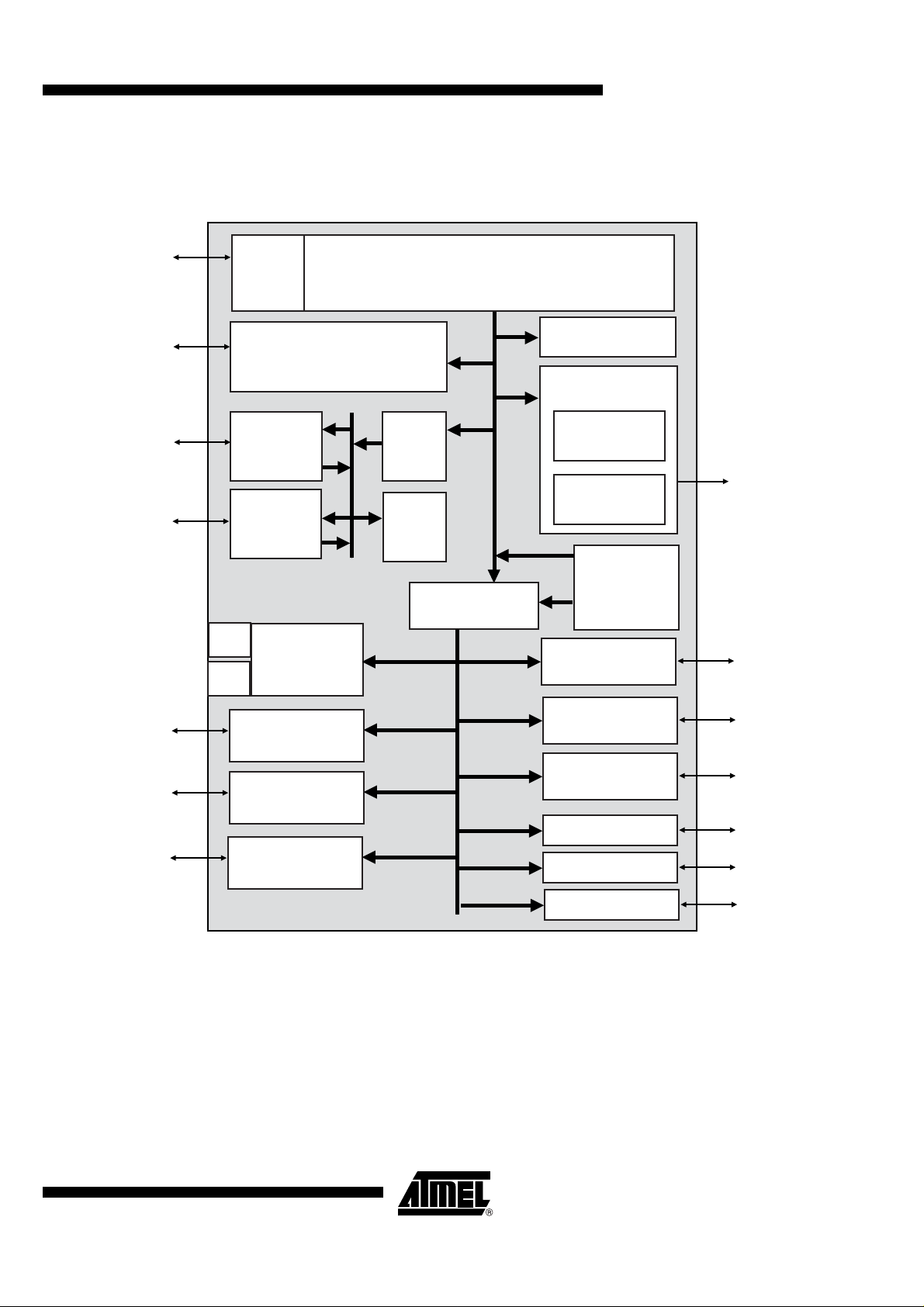
Block Diagram
AT75C221 Summary
Figure 3.
JTAG Debug
Audio Codec
and I/O Lines
AT75C221 Block Diagra m
Interface
MII PHY
Interface
MII PHY
Interface
ICE
Ethernet
10/100 Mbps
MAC Interface
Ethernet
10/100 Mbps
MAC Interface
OSC.
PLL
OakDSPCore
DSP Subsystem
System
Controller
ARM7TDMI MCU Core
ASB/ASB
Bridge
32k Bytes
SRAM
Peripheral Bridge
Boot ROM
External Bus
Interface
SDRAMC
SMC
Peripheral Data
Controller
SPI
16- or 32-bit data
Memory Bus
Serial Peripherals
Boot DataFlash
Interrupt and
Fast Interrupt
I/O Lines
I/O Lines
Advanced
Interrupt
Controller
PIO Controller A
PIO Controller B
USART A
USART B
Timer/Counter 0
Timer/Counter 1
Timer/Counter 2
Serial Port
Serial Port
PWM Signals
PWM Signals
PWM Signals
6033CS–INTAP–05/04
11

Application Example
M
Figure 4.
DSP Subsystem
32K x 16
Program RAM
Oak Program Bus Oak Data Bus
2K x 16 X-RAM
Codec Interface
2K x 16 Y-RAM
16K x 16
OakDSPCore
General-
purpose RAM
On-chip
Emulation
Module
256 x 16
Dual-port
Mailbox
Bus Interface Unit
Figure 5.
Network
PC
Speaker
icrophone
Handset
DSP Subsystem
ASB
Application Example Overview: Standalone Ethernet Telephone
Keyboard Screen
Ethernet
10/100 Mbps PHY
Ethernet
10/100 Mbps PHY
Speaker
Phone
Interface
Analog Front End
Voice
Codec
Dual-port
Ethernet
10/100 Mbps
MAC
Interface
Voice
Processing
DSP Subsystem
ARM7TDMI Core
VolP
Protocol
Stack
AT75C221
SDRAM
Controller
External Bus
Interface
SRAM
Controller
SDRAM
Flash
12
AT75C221 Summary
6033CS–INTAP–05/04

Functional
Description
AT75C221 Summary
ARM7TDMI Core
DSP Subsystem
The ARM7TDMI is a three-stage pipeline, 32-bit RISC processor. The processor architecture is Von Neumann load/store architecture, c haracterized by a single data and
address bus for instruc tions an d data . The CPU ha s two inst ruction sets: the ARM an d
the Thumb instruction set. The ARM instruction set has 32-bit wide instructions and provides maximum pe rformanc e. Thumb ins truction s are 16-bit wi de and give m aximum
code density.
Instructions operate on 8-bit, 16-bit and 32-bit data types.
The CPU has seven operating modes. Each operating mode has dedicated banked reg-
isters for fast exception handling. The processor has a total of 37 32-bit registers,
including six status registers.
The AT75C221 DSP subsystem is composed of:
• An OakDSPCore running at 60 MIPS
• 2K x 16 of X-RAM
•2K x 16 of Y-RAM
• 16K x 16 of General Purpose Data RAM
• 32K x 16 of Loadable Program RAM
• One 256 x 16 Dual-port Mailbox
• One Codec Interface
The DSP subsystem is fully autonomous. T he local X- and Y-RAM allow s it to reach its
maximum processing rate , and a local large data RAM enab les complex DSP algorithms to be impl eme nted . T he l ar ge size of the loadable p rogr am RAM pe r mit s the us e
of functions as complex as a low bit-rate vocoder.
Ethernet MAC
During boot time, the ARM7TDMI core has the ability to maintain the OakDSPCore i n
reset state and to uploa d DSP cod e. When the Oa kDSP Core rev erts to an active s tate,
this code is executed.
When the OakDSPC ore is run ning the dua l-port ma ilbox i s used as the c ommunic ation
channel between the ARM7TDMI and the OakDSPCore.
A programmable codec interface is directly connected to the OakDSPCore. It allows the
connection of most industrial voice, multimedia or data codecs.
The AT75C221 features two identi cal Ethernet MACs with the same attribut es as
follows:
• Compatible with IEEE Standard 802.3
• 10 and 100 Mbits per Second Data Throughput Capability
• Full- and Half-duplex Operation
• Media Independent Interface to the Physical Layer
• Register Interface to Address, Status and Control Registers
• DMA Interface
• Interrupt Generation to Signal Receive and Transmit Completion
• 28-byte Transmit and 28-byte Receive FIFOs
• Automatic Pad and CRC Generation on Transmitted Frames
6033CS–INTAP–05/04
13

• Address Checking Logic to Recognize Four 48-bit Addresses
• Supports Promiscuous Mode Where All Valid Frames are Copied to Memory
• Supports Physical Layer Management through MDIO Interface
The Ethernet MAC is the har dware i mpl em enta tio n of th e MA C su b- layer O SI refe re nce
model between the physical layer (PHY) and the logical link layer (LLC). It controls the
data exchange between a host and a PHY layer according to Ethernet IEEE 802.3u data
frame format. The Ethernet MAC contains the required logic and transmit and receive
FIFOs for DMA m anagement . In addi tion, it is inter faced thr ough MDIO /MDC pins for
PHY layer management. The Ethernet MAC transfers data in media-independent interface (MII).
Peripheral Multiple x ing
on PIO Lines
Power Supplies
System Controller
The AT75C2 21 feat ures tw o PIO Control lers , PIOA a nd PIO B, mul tiple xing I/ O lines of
the peripheral set.
The PIO Controller A m anages 32 I/O lin es, P A0 to PA31, b ut onl y the I/O lines PA0 to
PA12 PA19 and PA22 are available in the 208-lead package.
The PIO Controller B manages only 16 I/O lines, PB0 to PB15, but only the I/O lines
PB0 to PB9 are available in the 208-lead package.
Each I/O line of a PIO Controller can be multiplexed with a peripheral I/O.
The AT75C221 has three types of power supply pins:
• VDDCORE pins power the core, including the ARM7TDMI processor, the DSP
subsystem, the memories and the peripherals; voltage is between 1.65V and 1.95V,
1.8V nominal.
• VDDIO pins power the I/O lines, including those of the External Bus Interface and
those of the peripherals; voltage is between 3.0V and 3.6V, 3.3V nominal.
• VDDOSC pins power the PLL and oscillator cells; voltage is between 1.65V and
1.95V, 1.8V nominal.
Ground pins are common to all power supplies.
The AT75C221 features a System Controller, which takes care of and controls:
• The Test Mode
•The Reset
• The Clocks of the System
• The Chip Identifier
Memory Controller
14
AT75C221 Summary
The System Controller manages the reset of the entire system and integ rates a clock
generator made up of an oscillator and a PLL.
The AT75C221 architecture is made up of two Advanced System Buses, the ARM ASB
and the MAC ASB. Both handle a single memory space.
The ARM ASB handles the acc ess r equ ests of t he AR M7TD M I and th e PDC. It hand les
also the access reque sts comi ng from the MAC AS B. It connec ts with the Exter nal Bus
Interface, the Peripheral Bridge and the Internal Memories, including the mailbox with
the DSP Subsystem. It also connects with the MAC ASB.
The MAC ASB handles the access requests of the DMAs of both Ethernet MACs. It also
handles the access requests coming from the the ARM ASB. It connects essentially with
the Frame Buffer, but also connects with the ARM ASB.
6033CS–INTAP–05/04

AT75C221 Summary
The major advantage of this double-ASB architecture is that the Ethernet traffic does not
occupy the main ASB bandwidth, ensuring that the ARM7TDMI can perform at its maximum speed while the Ethernet traffic goes through the Frame Buffer.
Boot Program
Peripherals
PDC: Peripheral Data
Controller
The AT75C221 can boot in sev eral wa ys; inclu ding from i nternal boot soft ware and a
hardware connection of Data Flash. When t he ARM7TDMI processor is released fro m
reset, it basically attempts a fetch from address 0x00000000. Depending on the hardware configuration, the memory mapping can be altered and thus modify how the
system boots.
The Peripheral Bridge allows access to the embe dded peripheral user interface s. It is
optimized for low power consumption, as it is built without usage of any clock. However,
any access on the peripheral is performed in two cycles.
The AT75C221 peripherals are design ed to be prog rammed with a minimu m number of
instructions. Each peripheral has 16K bytes of address space allocated in the upper part
of the address space.
The AT75C221 features a six-chan nel Peripheral Data Controller (PDC) dedic ated to
the two on-chip UA RTs and the SPI . One P DC chan nel is c onnected to the re ceivin g
channel and one to the transmitting channel of each UART and of the SPI.
Each PDC channel operates as DMA (Direct Memory Access).
The User Interface of a PDC channel is integ rated i n the me mor y spa ce of eac h peri ph-
eral. It contains a 32-bit address pointer register and a 16-bit count register. When the
programmed number of bytes is transferred, an end- of-transfer signal is sent to the
peripheral and is vi sible in the p erip heral st atus regi ster . This st atus bit mig ht trigge r an
interrupt.
EBI: External Bus
Interface
SDRAMC: SDRAM
Controller
SMC: Static Memory
Controller
The External Bus Interface generates the signals which control access to external memories or peripheral devices. It contains two controllers: the SDRAM Controller and the
Static Memory Controller and mana ges the sh aring of data and address buses between
both controllers.
The SDRAM Controller extends the memory capabilities of a chip by providing the interface to an external 16- or 32-bit SDRAM device. The page size su ppor ts ranges from
2048 to 8192 and the number of columns from 256 to 2048. It supports byte (8-bit), halfword (16-bit) and word (32- bit) access es. The maximum addr essable SDRAM size is
256M bytes.
The SDRAM Controller suppor ts a read or wr ite burst length of one location. It keeps
track of the active row in each bank, thus maximizing SDRAM performance, e.g., the
application may be placed in one bank and data in the other banks. So as to optimize
performance, it is advisable to avoid accessing different rows in the same bank.
The SDRAM Controller’s function is to make the SDRAM device acc ess protocol tr ansparent to the user.
The AT75C221 features a S tati c Memor y Cont roll er that e nabl es interfacing with a wide
range of external static memory on peripheral devices, including Flash, ROM, static
RAM, and parallel peripherals.
The SMC provides a gl ueless memory interface to exter nal memory us ing common
address, data bus and dedic ated co ntrol sig nals. The SMC is hig hly progr ammab le and
6033CS–INTAP–05/04
15

has up to 24 bits of address bus, a 32- or 16-bit data bus and up to four chip select lines.
The SMC supports differ en t ac ce ss proto co ls al lowing single clock-cycle accesses. The
SMC is programme d as an internal peripheral that has a stand ard APB bus in terface
and a set of memory-mapped registers. It shares the external address and data buses
with the SDMC.
AIC: Advanced Interrupt
Controller
PIO: Programmable I/O
Controller
U ART: Universal
Asynchronous Receiver
Transmitter
The AT75C221 integrates an A dv anced Inter rupt Controller (AIC) which is con nected to
the fast interrupt requ est (nF IQ) a nd the stan dard in terr upt requ est ( nIRQ) inputs of th e
ARM7TDMI pro cessor . The proc essor’ s nFIQ lin e can on ly be ass erted by th e exter nal
fast interrupt request input (FIQ). The nIRQ line can be asserted by the interrupts generated by the on-chip peripherals and the two external interrupt request lines, IRQ0 to
IRQ1.
An 8-level priorit y encoder allo ws the user to def ine the priori ty between the differ ent
interrupt sources. Internal sources are p rogrammed to be level-s ensitive or e dge-triggered. Extern al so urces ca n be pro gramm ed to be po sitiv e- or neg ativ e-edge tr igger ed
or high- or low-level sensitive.
The AT75C221 integ rates 24 progr ammab le I/O pins. E ach pin can be programm ed as
an input or an output. Each pin can also generate an interrupt. The programmable I/O is
implemented as two blocks, called PIO A and PIO B, 32 and 16 pins each, respectively.
These pins are used for several functions:
• External I/O for internal peripherals
• Keypad controller function
• General-purpose I/O
The AT75C221 provides two identical full-duplex, Universal Asynchronous Receiver
Transmitters as UART A and UART B. These peripherals sit on the APB bus but are
also connected to the ASB bus (and hence external memory) via a dedicated DMA.
The main features of the UART are:
• Programmable Baud Rate Generator
• Parity, Framing and Overrun Error Detection
• Line Break Generation and Detection
• Automatic Echo, Local Loopback and Remote Loopback Channel Modes
• Interrupt Generation
• Two Dedicated Peripheral Data Controller Channels
• 6-, 7- and 8-bit Character Length
• Modem Control Signals
TC: Timer/Counter
16
AT75C221 Summary
The AT75C221 features a timer/counter block which includes three identical 16-bit
timer/counter channels. Each channel can be independently programmed to perform a
wide range of functions including frequency measurement, event counting, interval measurement, pulse generation, delay timing and pulse-width modulation.
Each timer/counter channel has thr ee externa l cloc k inputs , five inter nal cl ock in puts,
and two multi-purpose input/output signals that can be configured by the user. Each
channel drives an internal interrupt si gnal that ca n be programme d to generate processor interrupts via the AIC.
The timer/counter block has two global registers which act upon all three TC channels.
The Block Control Reg ister allows the three chan nels to be started sim ultaneo usly with
6033CS–INTAP–05/04

AT75C221 Summary
the same instruction. The Block Mode Register defines the external clock inputs for
each timer/counter channel, allowing them to be chained.
SPI: Serial Peripheral
Interface
The Serial Peripheral Interface circuit is a synchronous serial data link that provides
communication with exter nal devi ces in Maste r or Slave Mode. It als o allows com munication between processors if an external processor is connected to the system.
The Serial Peripheral Interface is essentially a shift register that serially transmits data
bits to other SPI's. During a data transfer, one SPI system acts as the “master”' which
controls the data flow, whi le the other system acts as the “s la ve '' wh ic h h as data sh ifte d
into and out of it by the master. Different CPU's can take turn being masters ( Multiple
Master Protocol opposi te to Single Master Protocol whe re one CPU is always the master while all of the others are always slaves), and one master may simultaneously shift
data into multiple slaves. However, only one slave may drive its output to write data
back to the master at any given time.
The main features of the SPI are:
• Four Chip Selects with External Decoder Support Allow Communication with Up to
15 Peripherals
• Serial Memories, such as DataFlash and 3-wire EEPROMs
• Serial Peripherals, such as ADCs, DACs, LCD Controllers, CAN Controllers and
Sensors
• External Coprocessors
• Master or Serial Peripheral Bus Interface
• 8- to 16-bit Programmable Data Length Per Chip Select
• Programmable Phase and Polarity Per Chip Select
• Programmable Transfer Delays Between Consecutive Transfers and Between Clock
and Data Per Chip Select
• Programmable Delay Between Consecutive Transfers
• Selectable Mode Fault Detection
• Connection to PDC Channel Capabilities Optimizes Data Transfers
• One Channel for the Receiver, One Channel for the Transmitter
6033CS–INTAP–05/04
17

Orderi ng Information
Table 2 below provides package ordering information for the AT75C221.
Table 2.
Ordering Code Package Operating Temperature Range
AT75C221-Q208 PQFP208 0° to 70° C
AT75C221-C256 BGA256 0° to 70° C
Ordering Informa tion
18
AT75C221 Summary
6033CS–INTAP–05/04

Mechanical Characteristics and Packaging Information
BGA Packaging Information
AT75C221 Summary
Figure 6.
AT75C221 BGA Package
∅b
6033CS–INTAP–05/04
For BGA package data, see Table 3 on page 20,
19

BGA Package Data
b
.
Table 3.
Symbol Min Nom Max
A1 0.50 0.60 0.70
∅
aaa 0.30
bbb 0.25
ccc 0.35
ddd 0.30
eee 0.15
A 1.92 2.13 2.34
B 0.28 0.32 0.38
D/E 26.8 27.0 27.2
D1/E1 24.0 24.7
e1.27
f8.05
Dimensions (mm)
0.60 0.75 0.90
20
AT75C221 Summary
6033CS–INTAP–05/04

PQFP Packaging Information
AT75C221 Summary
Figure 7.
PQFP Package Drawing
CC1
For package data, see Table 4, Table 5 and Table 6 on page 22.
6033CS–INTAP–05/04
21

PQFP Package Data
Table 4.
Symbol Min Nom Max
c 0.11 0.23
c1 0.11 0.15 0.19
L 0.65 0.88 1.03
L1 1.60 REF
R2 0.13 0.3
R1 0.13
S0.4
aaa 0.25
ccc 0.10
Table 5.
Max Min Min Nom Max Min Max Min Nom Max BSC BSC BSC BSC BSC BSC
4.10 0.25 3.20 3.40 3.60 0.17 0.27 0.17 0.20 0.23 31.20 28.00 31.20 28.00 0.50 0.10
Dimensions (mm)
Tolerances of Form and Position
Dimensions specific to PQFP Package (mm)
A A1 A2 b b1 D D1 E E1 e ddd
Table 6.
28 x 28 53 71 1.4 1.7 0.56 0.73 6.7 8.4 3.9 5.1
208-lead PQFP Package Electrical Characteristics
Body
Size
R (mΩ)C
MinMaxMinMaxMinMaxMinMaxMinMax
(pF) Cm (pF) Ls (nH) Lm (nH)
s
22
AT75C221 Summary
6033CS–INTAP–05/04

Atmel Corporation Atmel Operations
2325 Orchard Parkway
San Jose, CA 95131, USA
Tel: 1(408) 441-0311
Fax: 1(408) 487-2600
Regional Headquarters
Europe
Atmel Sarl
Route des Arsenaux 41
Case Postale 80
CH-1705 Fribourg
Switzerland
Tel: (41) 26-426-5555
Fax: (41) 26-426-5500
Asia
Room 1219
Chinachem Gol den P laza
77 Mody Road Tsimshatsui
East Kowloon
Hong Kong
Tel: (852) 2721-9778
Fax: (852) 2722-1369
Japan
9F, Tonetsu Shinkawa Bldg.
1-24-8 Shin kawa
Chuo-ku, Tokyo 104-0033
Japan
Tel: (81) 3-3523-3551
Fax: (81) 3-3523-7581
Memory
2325 Orchard Parkway
San Jose, CA 95131, USA
Tel: 1(408) 441-0311
Fax: 1(408) 436-4314
Microcontrollers
2325 Orchard Parkway
San Jose, CA 95131, USA
Tel: 1(408) 441-0311
Fax: 1(408) 436-4314
La Chantrerie
BP 70602
44306 Nantes Cedex 3, France
Tel: (33) 2- 40-1 8-18- 18
Fax: (33) 2- 40-18- 19-6 0
ASIC/ASSP/Smart Cards
Zone Industrielle
13106 Rousset Cedex, France
Tel: (33) 4- 42-5 3-60- 00
Fax: (33) 4- 42-53- 60-0 1
1150 East Cheyenne Mtn. Blvd.
Colorado Springs, CO 80906, USA
Tel: 1(719) 576-3300
Fax: 1(719) 540-1759
Scottish Enterprise Technology Park
Maxwell Building
East Kilbride G75 0QR, Scotland
Tel: (44) 1355-803-000
Fax: (44) 1355-242-743
RF/Automotive
Theresienstrasse 2
Postfach 3535
74025 Heilbro nn, Ge rmany
Tel: (49) 71-31-67-0
Fax: (49) 71-31-67-2340
1150 East Cheyenne Mtn. Blvd.
Colorado Springs, CO 80906, USA
Tel: 1(719) 576-3300
Fax: 1(719) 540-1759
Biometrics/Imaging/Hi-Rel MPU/
High Speed Converters/RF Datacom
Avenue de Rochepleine
BP 123
38521 Saint-Egreve Cedex, France
Tel: (33) 4-76-58-30-00
Fax: (33) 4- 76-58- 34-8 0
Literature Requests
www.atmel.com/literature
Disclaimer:
warranty which is detailed in Atmel’s Term s and Conditions located on the Com pany’s web site. The Company assumes no responsibility for any
errors which may appear in this document, reserves the right to change devices or specifications detailed herein at any time without notice, and
does not make any commitment to update the information contained herein. No licenses to patents or other intellectual proper ty of Atmel are
granted by the Company in connection with the sale of Atmel products, expressly or by implication. Atmel’s products are not authorized for use
as critical components in life support devices or systems.
© Atmel Corporation 2004. All rights reserved.
is the trademark of Atmel Corporation or its subsidiaries. ARM
marks of ARM Ltd. OakDSPCore
terms and product names may be the trademarks of others.
Atmel Corporation makes no warranty for the use of its products, other than those expressly contained in the Company’s standard
®
and combinations thereof, and DataFlash® are the registered trademarks, and SIAP™,
Atmel
®
is the registered trademark of DSP Corporation. Linux® is the registered trademark of Linus Torvalds. Other
®
, ARM7TDMI®, ARM® Thumb®, and ARM® Pow ere d® are the registered trade-
Printed on recycled paper.
6033CS–INTAP–05/04
0M
 Loading...