


Features
•
Fulfills IEC 1036, Class 1 Accuracy Requirements
•
Fulfills IEC 687, Class 0.5 and Class 0.2 Accuracy, with External Temperature
Compensated Voltage Reference
•
Simultaneous Active, Reactive and Apparent Power and Energy Measurement
•
Power Factor, Frequency, Voltage and Current Measurement
•
Single and Poly Phase Operation
•
Three Basic Operating Modes: Stand-Alone Mode, Microprocessor Mode and MultiChannel Mode
•
Flexible Interfacing, 8-bit Microprocessor Interface, 8-bit Status Output and Eight
Impulse Outputs
•
Calibration of Gain and Phase Error
•
Compensation of the Non-Linearity of Low Power Measurement
•
Adjustable Starting Current and Meter Constant
•
Measurement Bandwidth of 1000 Hz
•
Tamper Proof Design
•
Single +5V Supply
Description
A two chip solution, consisting of AT73C500 and AT73C501 (or AT73C502), offers all
main features required for the measurement and calculation of various power and
energy quantiti es in static Watt-h our meters. The dev ices operate acco rding to
IEC1036, class 1, specification. IEC 687, class 0.5 and 0.2 requirements are fulfilled
when used with external temperature compensated voltage reference.
The AT73C501 contains six, high-performance, Sigma-Delta analog-to-digital converters (ADC). The AT73C500 is based on an efficient digital signal processor (DSP) core
and it supports interfacing both with the AT73C501 and with an external microprocessor. The AT73C500 DSP can also be used with the differential input ADC, AT73C502.
With this chipset, only a minimum of discrete components is required to develop products ranging from si mple domestic Wa tt-hour meters to sop histicated indus trial
meters. The chipset can be used in single-pha se as well as in poly- phase systems .
The DSP core of th e AT73C500 is easy to co nfigure . By changi ng the mode of the
AT73C500, the device can be operate d in a stand-al one enviro nment or be used wit h
a separate contr ol proc essor . It i s als o pos sible to co nfigure the c ircui t to p erform the
functions of three independent single phase Wh meters.
The chips support calibration of gain and phase error. All calibrations are done in the
digital domain and no trimming components are needed. The calibration coefficients
are either stored in an EEPROM memory or supplied by an external microprocessor.
(continued)
Chip Set
Solution for
Watt-Hour
Meters
AT73C500 with
AT73C501 or
AT73C502
Rev. 1035A–08/98
1
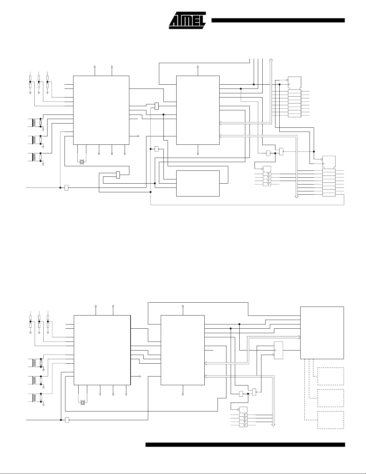
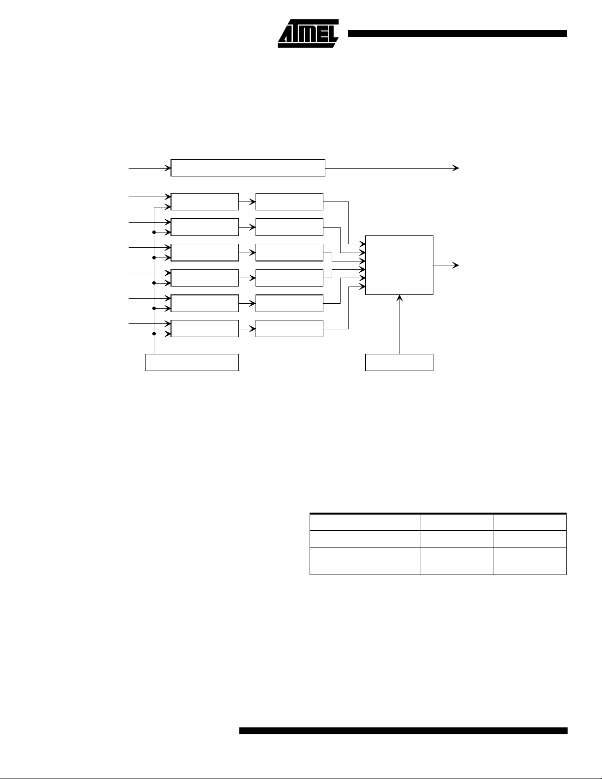
Figure 1.
Block diagram of the AT73C500 chipset in stand-alone configuration
EXTERNAL CONNECTOR
L1 L2 L3
L1
VREF
BGD
RESET
VI1
VI2
VI3
CI1
CI2
CI3
CS
VDA
VDDA
VCC
AT73501
SIX SINGLE-ENDED,
INDEPENDENT
SIGMA-DELTA
CONVERTERS
PFAIL
ACK
DATA
CLKR
CLK
AGND
BRDY
IRQ0
IRQ1
&
SIN
SCLK
XRES
L2
XI XO MODE
VSA
VSSA
GND
1
L3
RESET
&
1
CS
SK
The AT73C500 is progra mmed to m easure act ive, rea ctive
and apparent phase powers. Phase factors, phase voltages, phase currents and line frequenc y are also measured, simultaneously. Based on the individu al phase
powers, total active power is determined.
The power value s are calc ulated ove r one-li ne freque ncy
cycle. The negative and positive results are accumulated in
different registers, which allows for separate billing of
imported and e xported act ive energ y. Also, the reactive
results are sorted depending on whether capacitive or
inductive load is applied.
VCC
STROBE
RD/WR
DEDICATED DSP
DI
AT73500
FOR ENERGY
METERING
GND
AT93C46
EEPROM
128*8 bit
ADDR1
ADDR0
SOUT1
SOUT0
DATA BUS
STATUS BUS
DO
MODE2
MODE1
MODE0
1
1
1
1
1
-VArh
+VArh
-Wh
+Wh
+Wh
-Wh
+VArh
-VArh
&
Eight pulse outputs are provided. Each billing quantity
(+Wh, -Wh, +VArh, -Varh) is supplied with its own meter
constant output, as well as a display counter output. In
multi-channel mode, AT73C500 per forms the fu nctions of
three independent s ingle phase Wh me ters and three
impulse outputs are available, one for each meter element.
All measurement inform ation is av ailab le on an 8-bit microprocessor bus. The results are o utput in six packages, 16
bytes each. Mode and s tatus information of the meter is
also transferred with each data block.
TAMP
STUP
L3
L2
L1
FAIL
DATRDY
INI
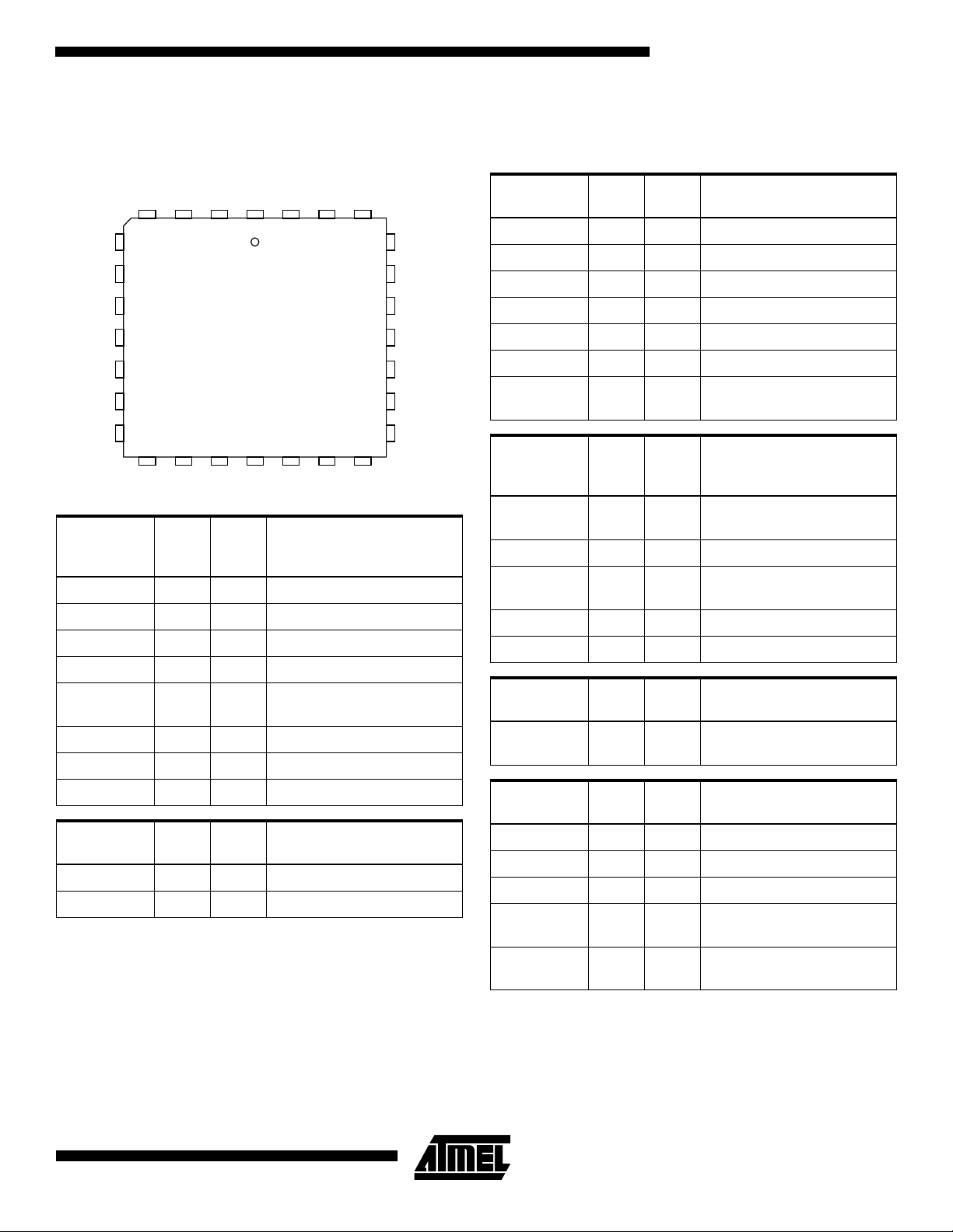
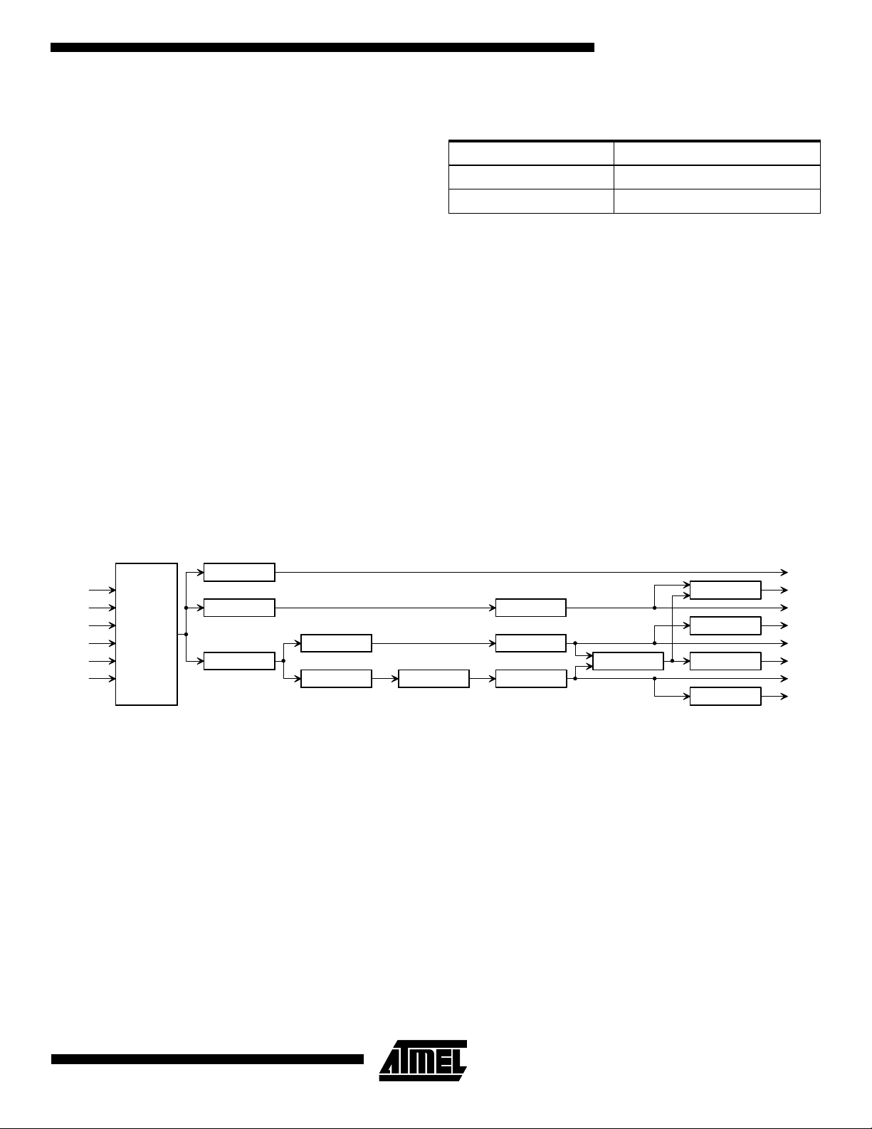
Figure 2.
L1 L2 L3
L1
L2
L3
RESET
2
Block diagram of the AT73C500 chipset in microprocessor configuration
VDA
VREF
BGD
RESET
1
VI1
VI2
VI3
CI1
CI2
CI3
CS
VDDA
AT73501
SIX SINGLE-ENDED,
INDEPENDENT
SIGMA-DELTA
CONVERTERS
XI XO MODE
VCC
VSA
VSSA
GND
PFAIL
ACK
DATA
CLKR
CLK
AGND
BRDY
IRQ0
IRQ1
SIN
SCLK
XRES
VCC
AT73500
DEDICATED DSP
FOR ENERGY
METERING
GND
STROBE
RD/WR
ADDR1
ADDR0
SOUT1
SOUT0
DATA BUS
STATUS BUS
MODE2
MODE1
MODE0
AT73C500
AT90Sxx
D
DATRDY
B9
&
1
1
1
1
1
B14
B13
B12
MICROCONTROLLER
MODEM
LCD
EEPROM
Pin Description
AT73C501 Single-ended ADC
AT73C500
Figure 3.
PFAIL
AGND
VREF
PLCC-28 package pin layout
34
5
BGD
6
CS
7
VCC
8
9
10
VCIN
11
VSSA VDDA AIN2 AIN4 AIN6 AIN1 AIN3
DATAFSRACKCLKRCLKXIXO
26272812
25
24
23
22
21
20
19
18171615141312
Power
Supply
Pins Pin I/O Description
VDDA 13 PWR Analog Supply, Positive, +5V
VSSA 12 PWR Analog Supply, Negative, 0V
VDA 21 PWR Analog Supply, Positive, +5V
VSA 20 PWR Analog Supply, Negative, 0V
AGND 9 PWR
Analog Ground Reference
Output
VREF 11 PWR Reference Voltage Output
VCC 7 PWR Digital Supply, Positive, +5V
VGND 23 PWR Digital Supply, Negative, 0V
Crystal Osc
Signals Pin I/O Description
XI 3 I Crystal Oscillator Input
XO 4 O Crystal Oscillator Output
RESET
MODE
GND
PD
VDA
VSA
AIN5
Analog
Signals Pin I/O Description
AIN1 17 I Input to Converter #1
AIN2 14 I Input to Converter #2
AIN3 18 I Input to Converter #3
AIN4 15 I Input to Converter #4
AIN5 19 I Input to Converter #5
AIN6 16 I Input to Converter #6
VCIN 10 I
Input to Voltage Monitoring
Block
Digital
Control
Signals Pin I/O Description
BGD 5 I
By-pass Control
for Reference Voltage
CS 6 I Chip Select Input
PD 22 I
Power Down Cont r o l
for A/D Modulators
MODE 24 I Mode Selection Control
RESET 25 I Reset Input, Active High
Status
Flags Pin I/O Description
PFAIL 8 O
Output of V olta ge Monitoring
Block
Output Bus
Signals Pin I/O Description
CLK 2 O Master Clock Output
CLKR 1 O Serial Bus Clock Output
DATA 26 O Serial Data Output
FSR 27 O
Output Sample Frame
Signal
ACK 28 O
Data Ready Acknowledge
Output
3
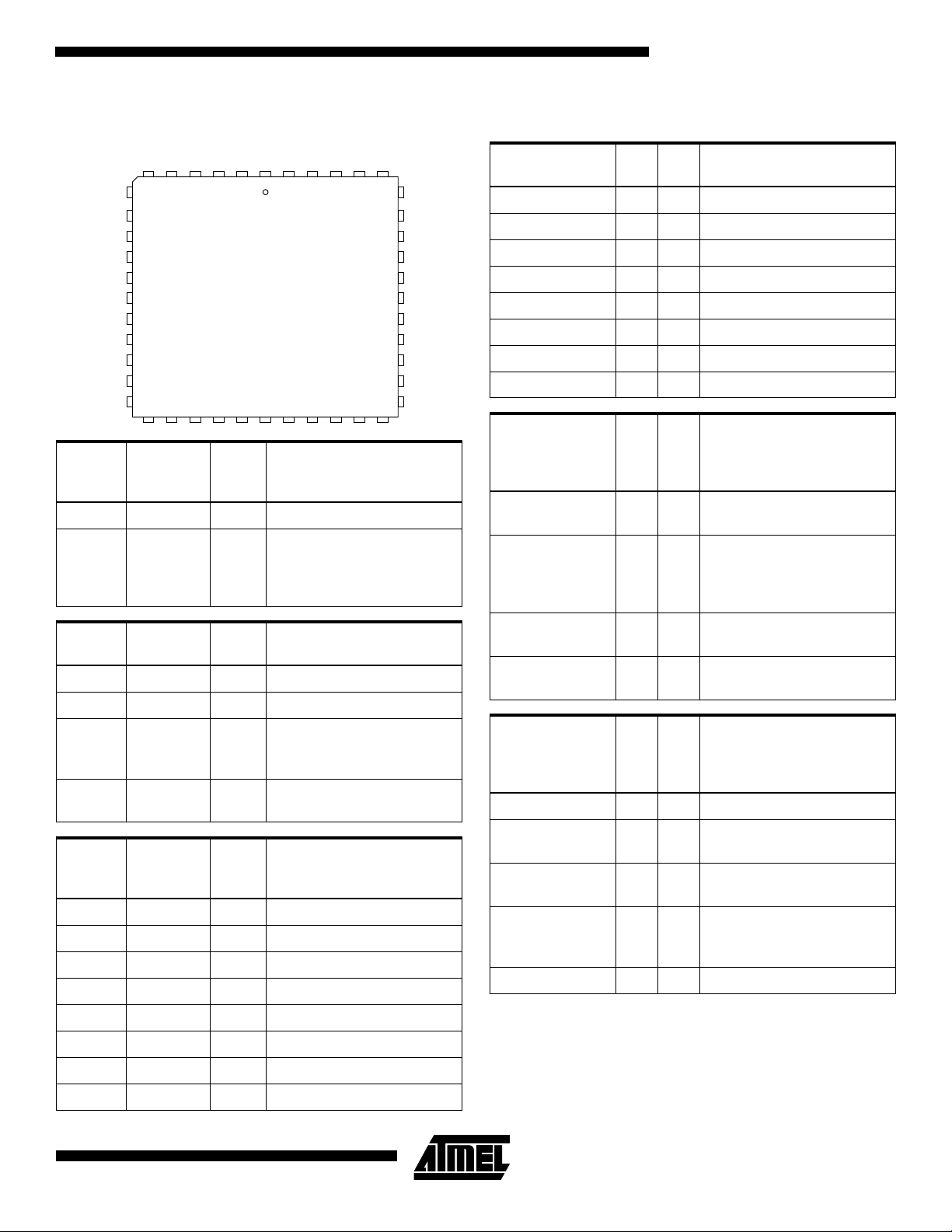
AT73C502 Differential-Ended ADC
T
A
A
Figure 4.
IADJUS
QFP-44 package pin layout
XI
BGD MODE
CS
VCC
VCC
PFAIL
AGND
VCIN
VREF
VS
VS
4344 42 41 40 39 38 37 36 35 34
133
3
4
5
6
7
8
9
10
11
1312 14 15 16 17 18 19 20 21 22
CLKRCLK
N/CN/CN/C
FSR
DATAACK
RESETXO
322
31
30
29
28
27
26
25
24
23
IINP2IINP1VINP3VINP2VINP1VDA
IINN1VINN3VINN2VINN1VDA
Power
Supply
Pins Pin I/O Description
VDA
VSA
AGND 6 PWR
12, 13,
29, 30
10, 11,
27, 28
PWR
PWR
Analog Supply, Positive, +5V
Analog Supply, Negative, 0V
Analog Ground Reference
Output
VREF 8 PWR Reference Voltage Output
VCC 3, 4 PWR Digital Supply, Positive, +5V
GND
PD
VDA
VDA
VSA
VSA
SINGLE
IINN3
IINP3
IINN2
Analog
Signals Pin I/O Description
VINP3 18 I Input to Converter #3 (+)
VINN3 19 I Input to Converter #3 (-)
IINP1 20 I Input to Converter #4 (+)
IINN1 21 I Input to Converter #4 (-)
IINP2 22 I Input to Converter #5 (+)
IINN2 23 I Input to Converter #5 (-)
IINP3 24 I Input to Converter #6 (+)
IINN3 25 I Input to Converter #6 (-)
VCIN 7 I
Input to Voltage Monitoring
Block
IADJUST 9 I Must be left floating
Digital
Control
Signals Pin I/O Description
BGD 1 I
By-pass Control for
Reference Voltage
CS 2 I Chip Select Input
PD 31 I
Power Down Control for A/D
Modulators
MODE 33 I Mode Selection Control
RESET 35 I Reset Input, Active High
Single / Differential selector.
SINGLE 26 I
· Low: Differential
· High or n/c: Single-ended
GND 32 PWR Digital Supply, Negative, 0V
Crystal
Osc
Signals Pin I/O Description
XI 43 I C rystal O scillator Input
XO 44 O Crystal Oscillator Output
Analog
Signals Pin I/O Description
VINP1 14 I Input to Converter #1 (+)
VINN1 15 I Input to Converter #1 (-)
VINP2 16 I Input to Converter #2 (+)
VINN2 17 I Input to Converter #2 (-)
4
AT73C500
Status
Flags Pin I/O Description
PFAIL 5 O
Output of Voltage Monitoring
Block
Output
Bus
Signals Pin I/O Description
CLK 41 O Master Clock Output
CLKR 3 9 O Serial Bus Clock Output
DATA 35 O Serial Data Output
FSR 36 O
ACK 37 O
Output Sample Frame
Signal
Data Ready Acknowledge
Output
AT73C500 DSP
AT73C500
Figure 5.
PLCC-44 package pin layout
GND
SOUT15SOUT0
6
GND ADDR0
7 39
B0
8
B1
9
B2
10
GND
11
GND
12
B12
13
B13
14
B14
15
GND
16
B15
17
18
B3
IRQ0 /
GND2GND1CLK44STROBE43VCC42ADDR241ADDR1
PFAIL
4
3
B419GND20B521B622B723N/C24B825B926GND27B10
40
38
37
36
35
34
33
32
31
30
29
28
Power
Supply
Pins Pin I/O Description
VCC 35, 42 PWR Digital Supply, Positive, +5V
1, 2, 6, 7,
GND
11, 12,16,
20, 27, 30,
PWR Digital Supply, Negative, 0V
34
Digital
Inputs Pin I/O Description
CLK 44 I C lock Input
XRES 38 I Reset Input, active low
Interrupt Input, usually
IRQ0 3 I
connected to PFAIL output
of AT73C 501
IRQ1 31 I
Interrupt Input, connected to
ACK Output of AT73C501
Status/
Mode
Bus Pin I/O Description
B15 17 I/O Status/Mode Bus, Bit7
B14 15 I/O Status/Mode Bus, Bit6
B13 14 I/O Status/Mode Bus, Bit5
B12 13 I/O Status/Mode Bus, Bit4
B11 29 I/O Status/Mode Bus, Bit3
XRES
BRDY
RD/WR
VCC
GND
SIN
SCLK
IRQ1 / ACK
GND
B11
Microprocessor
Bus Pin I/O Description
B7 23 I/O
B6 22 I/O
B5 21 I/O
B4 19 I/O
B3 18 I/O
B2 10 I/O
B1 9 I/O
B0 8 I/O
P Bus, Bit7
µ
P Bus, Bit6
µ
P Bus, Bit5
µ
P Bus, Bit4
µ
P Bus, Bit3
µ
P Bus, Bit2
µ
P Bus, Bit1
µ
P Bus, Bit0
µ
AT73C501 /
AT73C502 and
EEPROM
Interface Pin I/O Description
SOUT0 4 O
Serial Output, used as a
clock for EEPROM
Serial Output, used as Chip
SOUT1 5 O
Select (CS) for AT73C501
and as Data Input (DI) for
EEPROM
SIN 33 I
SCLK 32 I
Serial Data Input, data from
AT73C501 or from EEPROM
Serial Clock Input, bit clock
from AT73C501
Control Signals
of µµµµP Bus and
Status/Mode
Bus Pin I/O Description
STROBE 43 O Strobe Output
BRDY 37 I
ADDR1 40 O
Microprocessor ready for
I/O, Active Low
Address Output 1, used for
P bus
µ
Address Output 0, used for
ADDR0 39 O
Status/ Mode bus and for
Impulse Outputs
RD/WR 36 O Read/Write Signal
B10 28 I/O Status/Mode Bus, Bit2
B9 26 I/O Status/Mode Bus, Bit1
B8 25 I/O Status/Mode Bus, Bit0
5
AT73C501 and AT73C502
The AT73C501 consis ts of s ix, 16-b it anal og-to-d igital c onverters. The converters are equipped with single-ended
inputs. For di fferential ended applic ations, the AT73C50 2
chip is used.
The converters contain a reference vo ltage gen erator , voltage monitoring bl ock and se rial output i nterfac e. Both converters are based on high-performance, oversampling
Sigma-Delta modulators and digital decimation filters.
Figure 6.
Block diagram of the single-ended ADC chip, AT73C501
VOLTAGE
MONITORING
SIGMA-DELTA
MODULATOR
SIGMA-DELTA
MODULATOR
SIGMA-DELTA
MODULATOR
SIGMA-DELTA
MODULATOR
SIGMA-DELTA
MODULATOR
SIGMA-DELTA
MODULATOR
VOLTAGE
REFERENCE
DECIMATION
FILTER
DECIMATION
FILTER
DECIMATION
FILTER
DECIMATION
FILTER
DECIMATION
FILTER
DECIMATION
FILTER
In a 50 Hz meter, the nominal decimated sampling rate of
3200 Hz is used. This corresponds to 64 sa mpl es per eac h
line frequency cycle. 60 H z meters operate with 3840 Hz
sample rate. The master clock frequency of the ADC is
1024 times higher than the above frequencies, i.e. 3.2768
MHz in 50 Hz meters and 3.9321 6 MHz in 60 Hz system s.
The default meter constant of AT73C500 energy counters
is based on the above sample rates.
Other sample frequenci es can be used, bu t the energy
results have to be scaled accordingly. If higher sampling
rate is selected, the meter constant will also be increased
by the same ratio.
The three current inputs of AT73C501 are fed from secondary outputs of current transformers, from Hall sensors or
other similar sensors. In differential-ended applications,
such as with current shunt resistors, the AT73C502 ADC
can be used. On a ny of these converter s, the voltage
inputs must be equipped with simple external voltage dividers.
The input voltage range of each converter is 2V
PP
. The
characteristics of a Watt-hour meter operating, according to
IEC1036 specification, are based on a certain basic current, I
. As a default, the basic current of AT73C500
B
chipset is to 6.25% of the current input full scale value. This
means that if a meter is designed for I
= 5A
B
RMS
, the full
scale range of the current channels will be:
SERIAL OUTPUT
LOGIC
TIMING AND
CONTROL
100
-----------
IFS = 5 A
× 80 A
RMS
6.25
=
RMS
The following current transformer and voltage divider configuration is recommended for a 230V, 3-phase system,
with 5A basic current:
Voltage Inputs Current Inputs
Converter full-scal e input 2.0V
Corresponding full-scale
line voltage / current
270V
PP
RMS
2.0V
80A
PP
RMS
With the above settings, the nominal pulse rate of the
meter constant outp uts is 1250 impulses/kWh (1 250
impulses/kVArh) and the rate of four display outputs 100
impulses/kWh (100 imp/kVArh).
When used in a 5A transformer operated meter, the maximum current range ca n b e s c al ed down to 8A f or exam pl e.
In this case, the me ter constant wi ll be ten times hi gher
than in an 80A meter, i.e. 12500 impulses/kWh. Similarly,
the starting current level will be tra nsferred 2mA from
20mA.
6
AT73C500
AT73C500
If the nominal voltage is chosen to be 120V, the vo ltage
divider can either ha ve the same config uration as in the
230V meter, or it can be modified to produce 2.0V
pp
with
140V phase voltage. In the latter case, the default meter
constant will be roughly twice the constant of 230V meter,
i.e. 2411 impulses/ kWh. The mete r constan t can be s cale d
to an even number value by means of calibration.
As described above, th e config uration of voltag e divider s
and current trans form ers aff ects to a lmost all param eters
being metered, like energy counters and impuls e outputs.
A calibration coefficient is provided for the adjustment of
the display pulse rates. With this coefficient, the effect of
various voltage divider and current transformer configurations can be compensated. Care should be tak en that the
dynamic range of the A/D conve rters is a lways effectiv ely
utilized. The use o f calibrat ion coeff icients i s described in
the next section.
Current and voltage samples of AT73C501/AT73C502 are
multiplexed and transferred to AT73C500 through a serial
interface. The ti ming of the interf ace is presented in the
next section.
AT73C501/AT73C502 c ontai n an internal band gap v oltag e
reference. When used in cl ass 0.5 and 0.2 meter s, smaller
temperature drift is required. This can be achieved by
bypassing the internal reference and using temperature
compensated external reference instead. The reference is
selected with the BGD input.
BGD Reference
) Internal
0 (V
SS
1 (VDD) External
There is an integrated voltage mo ni tor ing blo ck on the converter chip. The PFAIL output is forced high if the level of
voltage supplied to V
input drops below 4.2V. There is a
CIN
hysteresis in the monitoring function and PFAIL returns low
if voltage at V
is raised back above 4.3V.
CIN
PFAIL output of AT73C501/AT73C502 can be connected
to an interrupt input o f AT73C500. A T73C500 det ects the
rising edge of PFAIL. To as sure reliable power -down procedure after voltage break, the V
supply of AT73C500
CC
must be equipped with a 470 µF or larger capacitor.
AT73C500
AT73C500 performs p ower and energy calculations. It a lso
controls the interfacing to the AT73C501 (or AT73C502)
and to an external microprocessor. The block diagram of
the DSP is presented below.
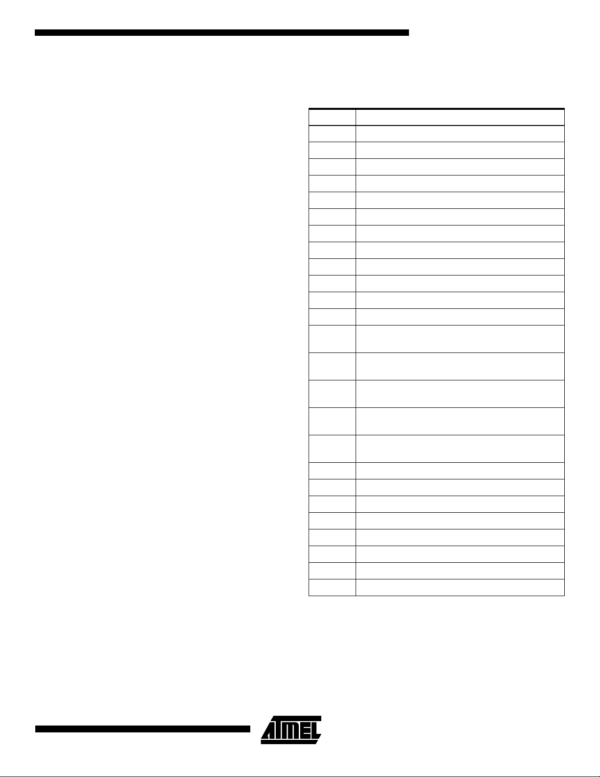
Figure 7.
u1(n)
u2(n)
u3(n)
i1(n)
i2(n)
i3(n)
Block diagram of DSP software
FREQUENCY
MEASUREMENT
VOLTAGE
MEASUREMENT
DC OFFSET
SUPPRESSION
PHASE
CALIBRATION
ACTIVE POWER
MEASUREMENT
HILBERT
TRANSFORM
REACTIVE POWER
MEASUREMENT
Serial Bus Interface
The timing of the serial bus interface connec ting the ADC
and DSP devices is presented in Figure 5. The same bus is
used to read the calibration data from an exter nal
EEPROM. This operation is described in section “Loading
of Calibration Coefficients” on page 19.
f
I
U
W
P
PF
Q
Wq
GAIN
CALIBRATION
GAIN AND OFFSET
CALIBRATION
GAIN AND OFFSET
CALIBRATION
APPARENT POWER
EVALUATION
CURRENT
DERIVATION
ACTIVE ENERGY
CALCULATION
POWER FACTOR
DERIVATION
REACTIVE ENERGY
CALCULATION
When the three current and three voltage samples are
ready, AT73C50 1/AT73C502 raises the ACK output.
AT73C500 detects the ri sing edge of ACK, and, after a f ew
clock cycles, it i s ready to read the sample s through the
serial bus. Th e transfer is initiated by CS/SOUT1 signal
and the data bits are strobed in at the falling edge of
CLKR/SCLK clock. Six 16-bit samples is transferred in the
following sequence: I1, U1, I2, U2, I3 and U3.
7
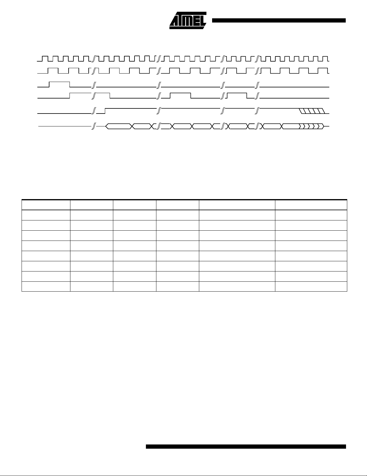
Figure 8.
CLK
CLKR
ACK
FSR
CS
DATA
Serial bus timing
CH1, B15
MSB
6 * 16 BITS
CH1, B14 CH1, B0
LSB
CH2, B15
MSB
CH2, B0
LSB
CH6, B1 CH6, B0
Operating Modes of AT73C500
The AT73C500 chips et has six operating modes. The
mode is selected by three mode control inputs which
AT73C500 reads through a bus during the initialization procedure after a reset state. The operation of
AT73C501/AT73C502 is independent of the mode
selected.
Mode Number Mode Bit 2 Mode Bit 1 Mode Bit 0 Operating Mode Calibration Data Storage
0 000 Not in use
In operating mode 7, the default display pul se rate is 10
impulses per kWh, instead of 100 impulses per kWh, as in
other modes.
1 0 0 1 Normal operation EEPROM
2 0 1 0 Multi-channel operation EEPROM
3 0 1 1 Normal operation Micro-processor
4 1 0 0 Multi-channel operation Micro-processor
5 101 Test mode None
6 110 Not in use
7 1 1 1 Normal operation EEPROM
Normal Measurement Mode
AT73C500 devices support both stand-alone and microprocessor configurati on. The cal ibrat ion coe fficient s ca n either
be supplied by a processor or stored in an 128 x 8-bit
EEPROM. The ROM is interfaced with AT73C500 via three
pin serial bus. AT73C500 and the processor communicate
through an 8-bit bus.
The only operational difference be tween stand- alone and
µP mode is the way of readi ng c al ib ra tio n c oeffi c ien ts. This
allows various combinations of these two configurations to
be utilized. For example, th e calibratio n data can be store d
in an EEPROM even though the processor reads and displays the measurement results supplied by AT73C500
device.
In most cases, the use of external EEPROM gives flexibility
to the meter testing and calibra tion, and also makes the
processor inte rface easier to implement. Th erefore, th is
configuration is recommended even in meters equipped
with a separate microprocessor.
The same sequence of basic ca lculations is performed
both in poly-phase and single-phase meters. This
sequence consists of DC offset suppression, phase, gain
and offset cal ibr atio n, ca lcul atio ns of m easu remen t qu ant ities and data transfer to µP bus and pulse outputs.
AT73C500 constantly m oni tor s v ar ious ta mpe ri ng an d faul t
situations, which are indicated by status bits.
After a reset state, AT73C500 goes through an initialization
sequence. The device reads the operating mode and
fetches the calibration coefficients an d adjustment factors
for output pulse rate and starting current level, either from a
non-volatile memory or from a microprocessor. After that
the normal measurement starts. The reset state is normally
activated by power-up reset following the recovery from a
voltage interruption.
8
AT73C500
AT73C500
Measurements and Calculations
The first operation performed by AT73C500 is digital highpass filtering. The purpose of the filtering is to remove the
DC offset of both current and voltage samples.
From offset free samples, active power i s calculated
phase-by-phase with simple multiplication and additio n
operations.
First, the current samples are multiplied by voltage samples. The multiplic ation resu lts are s ummed ov er one lin e
period and finally the sum value is divided by 64. This discrete time operation gives the average power of one
50/60Hz period and the result corresponds to the following
continuous time formula:
N
T
1
---
P
ANUNsin n wt
=
×
∑
n0
∫
T
0
=
N
1
=
-- -
A
∑
n0
=
nAnUnIn
2
A
×{}
N
I
sin n wt
×××××[]
N
cos
∅
()×××××
n
dt
∅+×N{}
where
T = 1/50 Hz or 1/60 Hz,
n = 1, 2, 3,..., 20 (basic 50/60 Hz frequency and the
harmonics),
= frequency response of calculations.
A
n
The total power is calculated by summing the power of
each line phase. Reactive power calculation is based on a
similar procedure. Before multipl ying the current an d voltage samples AT73C500 performs a frequency independent
-90 degree phase shift of the voltage signal. This is realized
with a digital Hilbert transformation filter. The bandwidth of
reactive power measuremen t is limited to 360 Hz.
Based on the active and reactive results apparent power
and power factors are d etermined. RMS phase voltages
are calculated by squaring and summing the voltage samples and fina lly tak ing a s quare r oot of the re sults. Curr ent
is determined by divi ding apparent po wer result by cor responding phase voltage.
Frequency measurement is based on a comparison of the
line frequency and AT73C500 sampling clock frequency.
The measurement range is from 20 Hz to 350 Hz.
All measurements and calculations, except frequency measurement, are made ov er 1 0 l ine cy cle per io ds . The resu lts
are updated and transferred to processor bus once in 200
ms.
Measurement Registers
For the measurement parameters 25 registers are allocated:
Register Meaning
REG0 Phase 1, active power, P1(10T), 32-bit register;
REG1 Phase 2, active power, P2(10T), 32-bit register;
REG2 Phase 3, active power, P3(10T), 32-bit register;
REG3 Phase 1, reactive power, Q1(10T), 32-bit register;
REG4 Phase 2, reactive power, Q2(10T), 32-bit register;
REG5 Phase 3, reactive power, Q3(10T), 32-bit register;
REG6 Phase 1, apparent power, S1(10T), 16-bit register;
REG7 Phase 2, apparent power, S2(10T), 16-bit register;
REG8 Phase 3, apparent power, S3(10T), 16-bit register;
REG9 Phase 1, power factor, PF1, 16-bit register;
REG10 Phase 2, power factor, PF2, 16-bit register;
REG11 Phase 3, power factor, PF3, 16-bit register;
REG12
REG13
REG14
REG15
REG16
REG17 Frequency, f, 16-bit register;
REG18 Reserved for further use, 16-bit register;
REG19 Phase 1, voltage U1, 16-bit register;
REG20 Phase 2, voltage U2, 16-bit register;
REG21 Phase 3, voltage U3, 16-bit register;
REG22 Phase 1, current I1, 16-bit register;
REG23 Phase 2, current I2, 16-bit register;
REG24 Phase 3, current I3, 16-bit register.
Active e xported energy since the lates t reset, +Wp ,
32-bit counter;
Active imported energ y s ince the l atest re set, -Wp,
32-bit counter;
Reactive energy, inductive load, Wqind, 32-bit
counter;
Reactive energy, capacitive load, Wqcap, 32-bit
counter;
Number of 10T periods elapsed since the latest
reset, 32-bit counter;
The size of the registers is either 16-bit or 32-bit. IEC specifications apply to the calculations of active and reactive
power and energy (REG 0-5 and REG 12-15). Other results
are intended mainly for demand recording and for va rious
diagnostic and display functions. The accuracy of those are
limited due to the finite resolution.
9
 Loading...