

Features
High Performance
•
System Speeds > 100 MHz
Flip-Flop Toggle Rates > 250 MHz
1.2 ns/1.5 ns Input Delay
3.0 ns/6.0 ns Output Delay
Up to 204 User I/Os
•
Thousands of Registers
•
Cache Logic® Design
•
Complete/Partial In-System Reconfiguration
No Loss of Data or Machine State
Adaptive Hardware
Low Voltage and Standard Voltage Operation
•
5.0 (V
3.3 (V
Automatic Component Generators
•
Reusable Custom Hard Macro Functions
Very Low Power Consumption
•
Standby Current of 500 µA/ 200 µA
Typical Operating Current of 15 to 170 mA
Programmable Clock Options
•
Independently Controlled Column Clocks
Independently Controlled Column Resets
Clock Skew Less Than 1 ns Across Chip
Independently Configurable I/O (PCI Compatible)
•
TTL/CMOS Input Thresholds
Open Collector/Tri-state Outputs
Programmable Slew-Rate Control
I/O Drive of 16 mA (combinable to 64 mA)
Easy Migration to Atmel Gate Arrays for High Volume Production
•
= 4.75V to 5.25V)
CC
= 3.0V to 3.6V)
CC
AT6000/LV Series
Coprocessor
Field
Programmable
Gate Arrays
Description
AT6000 Series SRAM-Based Field Programmable Gate Arrays (FPGAs) are ideal for
use as reconfigurable coprocessors and implementing compute intensive logic.
Supporting system speeds greater than 100 MHz and using a typical operating current
of 15 to 170 mA, AT6000 Series devices are ideal for high-speed, compute-intensive
designs. These FPGAs are designed to implement Cache Logic®, which provides the
user with the ability to implement adaptive hardware and perform hardware acceleration.
The patented AT6000 S eries architecture employs a symmetrical grid of small yet
powerful cells connected to a fl exible busing network. Independently controlled clocks
and resets gover n every column of cells. T he ar ray is su rrounded by programmable
I/O.
(continued)
AT6000 Series Field Programmable Gate Arrays
Device AT6002 AT6003 AT6005 AT6010
Usable Gates 6,000 9,000 15,000 30,000
Cells 1,024 1,600 3,136 6, 400
Registers (maximum) 1,024 1,600 3,136 6, 400
I/O (maximum) 96 120 108 204
Typ. Operating Current (mA) 15-30 25-45 40-80 85-170
Cell Rows x Columns 32 x 32 40 x 40 56 x 56 80 x 80
AT6000 and AT6000LV Series
0264E
2-3
Description
(Continued)
Devices range in size from 4,000 to 30,000 usable gates,
and 1024 t o 6400 registe rs. Pin locations ar e consistent
throughout the AT6000 Series for easy design migration.
High-I/O versions are available for the lower gate count
devices.
AT600 0 Series F PGAs utili ze a re liable 0. 6 µm singlepoly, double-metal CMOS process and are 100% factorytested.
Atmel’s PC- and workstation-based Integrated Development System is used to create AT6000 Series designs.
Multiple design entry methods are supported.
The Atmel architecture was developed to provide the highest levels of performance, functional density and design
flexibility in an FPGA. The cells in the Atmel array are
small, very efficient and contain the most important and
most commonly used logic and wiring functions. The cell’s
small s ize leads t o arrays with large numbers o f cel ls,
greatly multiplying the functionali ty in each cel l. A simple,
high-speed busing networ k provides fast, efficient communication over medium and long distances.
Figure 1.
Symmetrical Array Surrounded by I/O
The Symmetrical Array
At the heart of the Atmel architecture is a symmetrical array of identical cells (Fig ure 1). The array is continuous
and completely unint errupt ed from one edge to the other,
except for bus
2).
In addition to logic and storage, cells can also be used as
wires to connect functions together over short distances
and are useful for routing in tight spaces.
repeaters
spaced every eight cells (Figure
The Busing Network
There are two kinds of buses: local and express (see Figures 2 and 3).
Local buses are the link between the array of cells and the
busing network. There are two local buses— North-South
1 and 2 (NS1 and NS2)— for every column of cells, and
two local buses— East-West 1 and 2 (EW1 and EW2)—
for every row of cells. In a sector (an 8 x 8 array of cells
encl osed by rep eaters) e ach local bus is conne cted to
every cell in its column or row, thus providing every cell in
(continued)
2-4
AT6000/LV Series
Figure 2. Busing Network (one sector)
AT6000/LV Series
CELL
REPEATER
Figure 3. Cell-to-Cell and Bus-to-Bus Connections
2-5
Descr i pti on
(Continued)
the array with read/write access to two North-South and
two East-West buses.
Each cell, in addition, provides the ability to route a signal
on a 90° turn between the NS1 bus and EW1 bus and
between the NS2 bus and EW2 bus.
Express buses a re not connec ted directly t o cells, and
thus provide higher speeds. They are the fastest way to
cover long, straight-line distances within the array.
Each express bus is pa ired with a local bus, so there are
two ex press buses for eve ry colum n and two ex press
buses for every row of cells.
Conne ctive units, called r epeaters, spaced e very eight
cells, divide each bus, both local and express, into segments spanning eight cells. Repeaters are aligned in rows
and columns thereby partitioning the array into 8 x 8 sectors of cells. Each repeater is associated with a local/express pair, and on each side of the repeater are connections to a local-bus segment and an express-bus segment.
The repeater can be prog rammed to provide an y one of
twenty-one connecting functions. These functions are
symmetric with respect to both the two repeater sides and
the two types of buses.
Among the functions provided are the ability to:
• Isolate bus segments from one another
• Connect two local-bus segments
• Connect two express-bus segments
• Implement a local/express transfer
In all of these cases, each connect ion pr ovid es signal regene ration and is thu s unidi rectio nal. For bidi rect ional
connections, the basic repeater function for t he N S2 and
EW2 repeaters is augmented with a special programmable conne ction allowing bidirectiona l communication between local-bus segments. This option is primarily used to
implement long, tri-state buses.
Figure 4. Cell Structure
The Cell Structure
The Atmel cell (Figure 4) i s simple and small and yet can
be pr ogrammed to perform all the logic an d wiring functions needed to implement any digital circuit. Its four sides
are functionally identical, so each cell is completely symmetrical.
Read/write access to the four local buses— NS1, EW1,
NS2 and EW2— is controlled, in part, by four bidirectional
pass gates co nnected directly to the buses. To read a local bus, the pass gate for that bus is turned on and the
three-input multiplexer is set accordingly. To write to a local bus, the pass gate for that bus and the pass gate for
the associated tri-state driver are both turned on. The twoinput multiplexer supplying the control signal to the drivers
permits either: (1) active drive, or (2) dynamic tri-stating
controlled by the B input. Turning between L
or between L
NS2
and L
is accomplished by turning on
EW2
the two associated pass gates. The operations of reading,
writing and tur ning are subject to the restriction that e ach
bus can be involved in no more than a single operation.
In addition to the fo ur local-bu s connections, a cell receives two inputs and provides t wo outputs to each of its
North (N), South (S), East (E) and West (W) neighbors.
These inputs and outputs are divided into two classes: “A”
and “B.” There is an A input and a B input from each neighboring cell and an A output and a B out put driving all four
nei ghbor s. Be twee n cell s, a n A ou tput is alway s connected to an A input and a B output to a B input.
Within the cell, the four A inputs and the four B inputs enter
two separate, independently configurable multiplexers.
Cell flexibility is enhanced by allowing each multiplexer to
select also the logical constant “1.” The two multiplexer
outputs enter the two upstream AND gates.
Downstream from these two AND gates are an ExclusiveOR (XOR) gate, a register, an AND gate, an inve rter a nd
two four-input multiplexers producing the A and B outputs.
These multiplexers are co ntroll ed in tandem (unli ke the A
and B input multiplexers) and determine the function of the
cell.
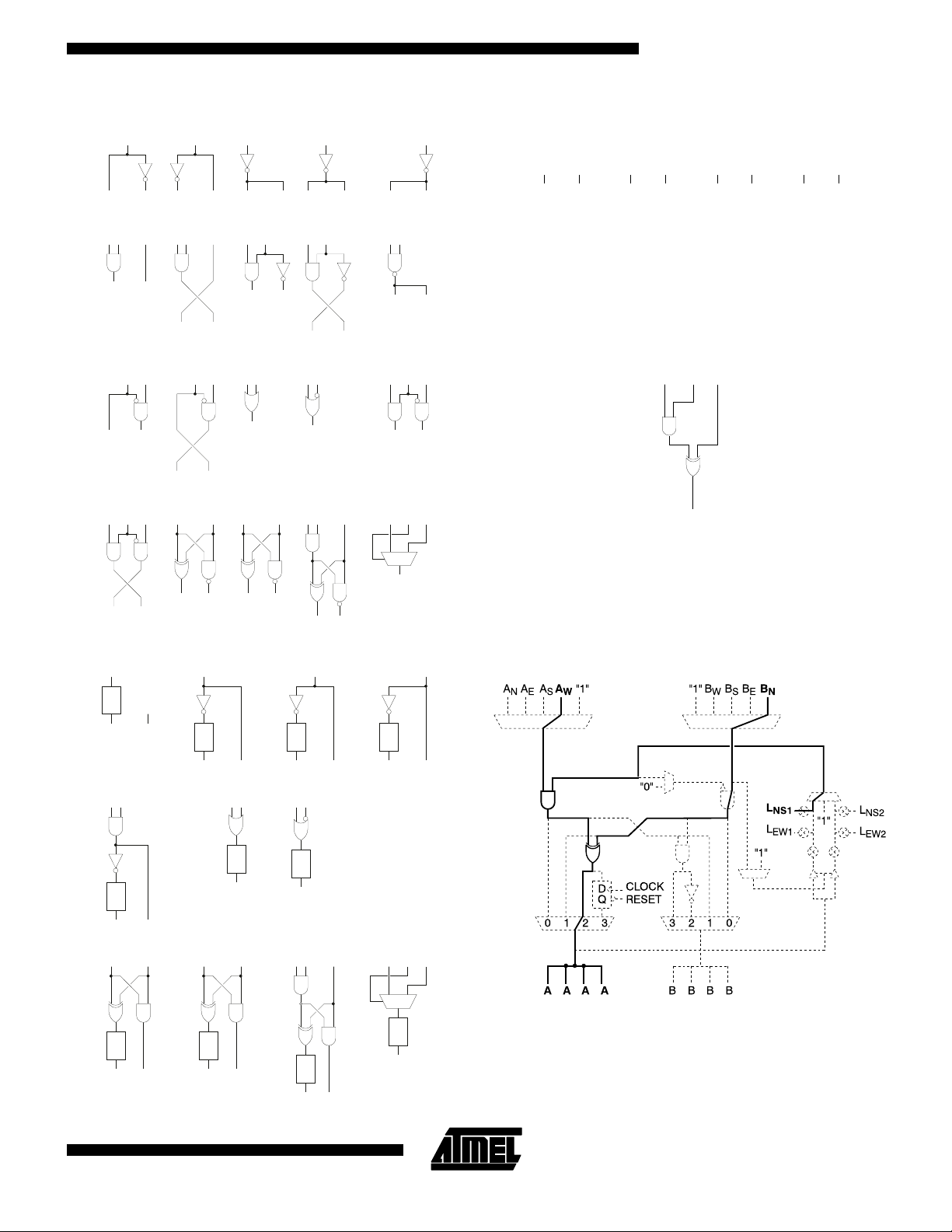
• I n State 0— correspond ing to the “0" inputs of the mul-
tiplexers— the output of the left-hand upstream AND
gate is connected to the cel l’s A output, and the out put
of the right-hand upstream AND gate is connected t o
the cell’s B output.
• I n State 1— correspond ing to the “1" inputs of the mul-
tiplexers— the output of the left-hand upstream AND
gate is connected to the cell’s B output, the output of the
right-hand upstream AND gate is connected to the cell’s
A output.
• I n State 2— correspond ing to the “2" inputs of the mul-
tiplexers— the XOR of the outputs from the two upstream AND gates is provided to the cell’s A output,
and L
NS1
(continued)
EW1
2-6
AT6000/LV Series
AT6000/LV Series
Figure 5a. Comb ina torial Ph y s ical Sta te s
L
i
A, L
o
A
L
i
A, L
o
L
i
A, L
o
L
i
A, L
o
BB
BABBA
B
B
B
BA
B
A, L
A, L
A, L
A, L
L
o
L
i
o
L
o
o
A
i
BB
A, L
o
L
i
B
A, L
o
BB A
L
A, L
i
o
i
B
L
BA
B
A, L
B
i
B
o
A, L
A
A, L
A, L
A, L
L
i
o
L
i
o
L
i
o
L
i
o
Figure 5b. Register States
A
A
L
i
B
BA
B
A, L
A
A, L
A, L
A, L
o
L
o
L
1BA0
B
B
i
B
o
BA
L
i
B
i
o
B
Figure 5c. Physical Constants
"0" "0"
A, L
o
B
"0" "1"
o
"1" "0"
B
A, L
B
o
Figure 6a. Two -Input AND Feeding XOR
A
BL
i
A
Figure 6b. Cell Configuration (A•L) XOR B
"1" "1"
A, L
o
BA, L
D
Q
A, L
o
A
L
D
Q
A, L
A
D
Q
A, L
"0"
i
o
B
o
B
B
B
D
Q
A, L
o
L
i
D
Q
A, L
D
Q
A, L
B
BA
L
i
D
Q
A, L
A, L
o
BA
B
o
A, L
B
o
L
i
D
Q
o
BA
L
i
D
Q
B
o
D
Q
A, L
o
1
D
Q
A, L
B
B
L
i
0
o
2-7
Description
(Continued)
while the NAND of these two outputs is provided to the
cell’s B output.
In State 3— corresponding to the “3" inputs of the mul-
•
tiplexers— the XOR function of State 2 is provided t o
the D input of a D-type flip-flop, the Q output of which is
connected to t he cell’s A o utput. Clock and asyn chronous reset signals are supplied externally as described
later. The AND of the out puts f rom the two upstream
AND gates is provided to the cel l’s B output.
Logic St ate s
The Atmel cell implements a rich and powerful set of logic
functions, stemming from 44 logical cell states which permutate into 72 physical states. Some states use both A
and B inputs. Other states are created by selecting the “1"
input on either or both of the input multiplexers.
Ther e are 28 com binator ial primitive s created fr om the
cell’s tri-state capabilities and the 20 physical states represented in the Figure 5a. Five logical primitives are derived
from the physical constants shown in Figure 5c. More
complex functions are creat ed by using cells in combination.
A two-input AND feeding an XOR (Figure 6a) is produced
using a single cell (Figure 6b). A two-to- one multiplexer
selects the logical constant “0" and feeds it to the righthand AND gate. The AN D gate acts as a feed-through,
letting the B input pass through to t he XOR. The three-toone multiplexer on the right side select s the local-bus input, L
and L
put of the AND gate fee ds int o the XOR, producing the
logic state (A•L) XOR B.
Figure 7.
, and passes it to the left-hand AND gate. The A
NS1
signals are the inputs to the AND gate. The out-
NS1
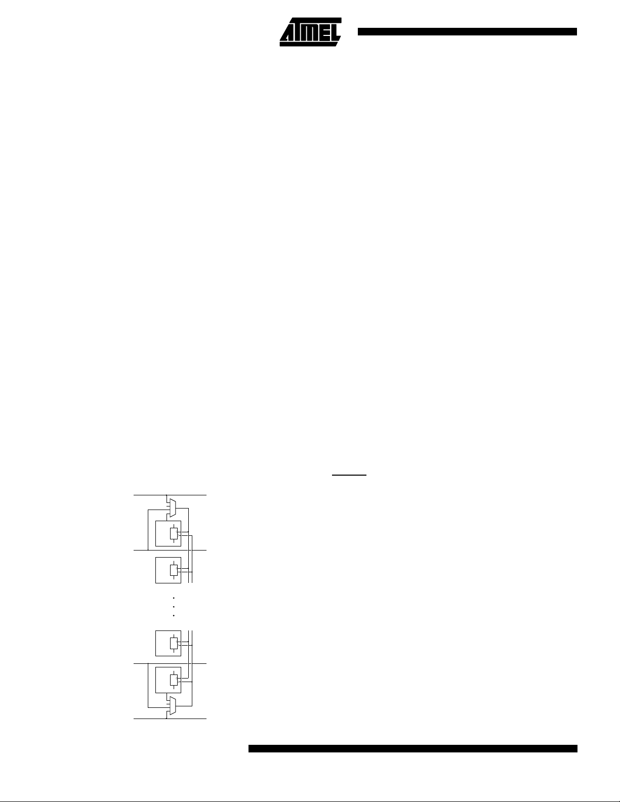
Column Clock and Column Reset
GLOBAL
CLOCK
EXPRESS
BUS
EXPRESS
BUS
GLOBAL
RESET
"1"
CELL
CELL
CELL
CELL
"1"
A
D
Q
D
Q
D
Q
D
Q
A
D
E
D
I
C
A
T
E
D
R
B
O
U
U
R
T
I
I
E
N
D
G
GLOBAL
CLOCK
EXPRESS
BUS
EXPRESS
BUS
GLOBAL
RESET
Clock Di str ibu tio n
Along the to p edge of the array is logic for d istributing
clock signals to the D flip-flop in each logic cell (Figure 7).
The distributi on net work is organized by column and per mits columns of cel ls to be independently clocked. At the
head of each column is a user-configurable multiplexer
providing the clock signal for that column. I t has four inputs:
Global clock supplied through the CLOCK pin
•
Express bus adjacent to the di stribution logic
•
“A” output of the cell at the head of the column
•
Logical constant “1" to conserve power (no clock)
•
Through the global clock, the network pr ovides low-skew
distribution of an externally supplied clock to any or al l of
the columns of the array. The global clock pin is also connected directly to the array via the A input of the upper left
and right corner cells (AW on the left, and AN on t he right).
The express bus is useful in distributing a secondary clock
to multiple columns when the global clock line is used as
a prim ary clock. The A output of a cell is useful in providing
a clock signal to a single column. The constant “1" is used
to reduce power dissipation in columns using no registers.
Asynchronous Reset
Along the bottom edge of the array is logic for asynchronously resetting the D flip-flops i n the logic cell s (Figure 7).
Like the clock network, the asynchronous reset network is
or ganized by column and per mits col umns to be independently reset. At the bottom of each column is a userconfigurable multiplexer providing the reset signal for that
column. It has four inputs:
Global asynchronous reset supplied through the
•
RESET pin
Express bus adjacent to the di stribution logic
•
“A” output of the cell at the fo ot of the column
•
Logical constant “1"to conserve power
•
The asynchronous reset logic uses these f our inputs in the
same way that the clock distribution logic does. Through
the global asynchronous reset, any or all columns can be
reset by an ext ernally supplied signal. The global asynchronous reset pi n is also connected directly to t he ar r ay
via the A input of the lower left and right corne r cells (AS
on the left, and AE on the right) . The e x press bus can be
used to distribute a seconda ry reset to m ultiple columns
when the gl obal r eset line is used as a primary reset, the
A output of a cell can also provide an asynchronous reset
signal to a single column, and the constant “1" is used by
columns with registers r equi ring no reset. All r egister s are
reset during power-up.
(continued)
2-8
AT6000/LV Series
AT6000/LV Series
Description
(Continued)
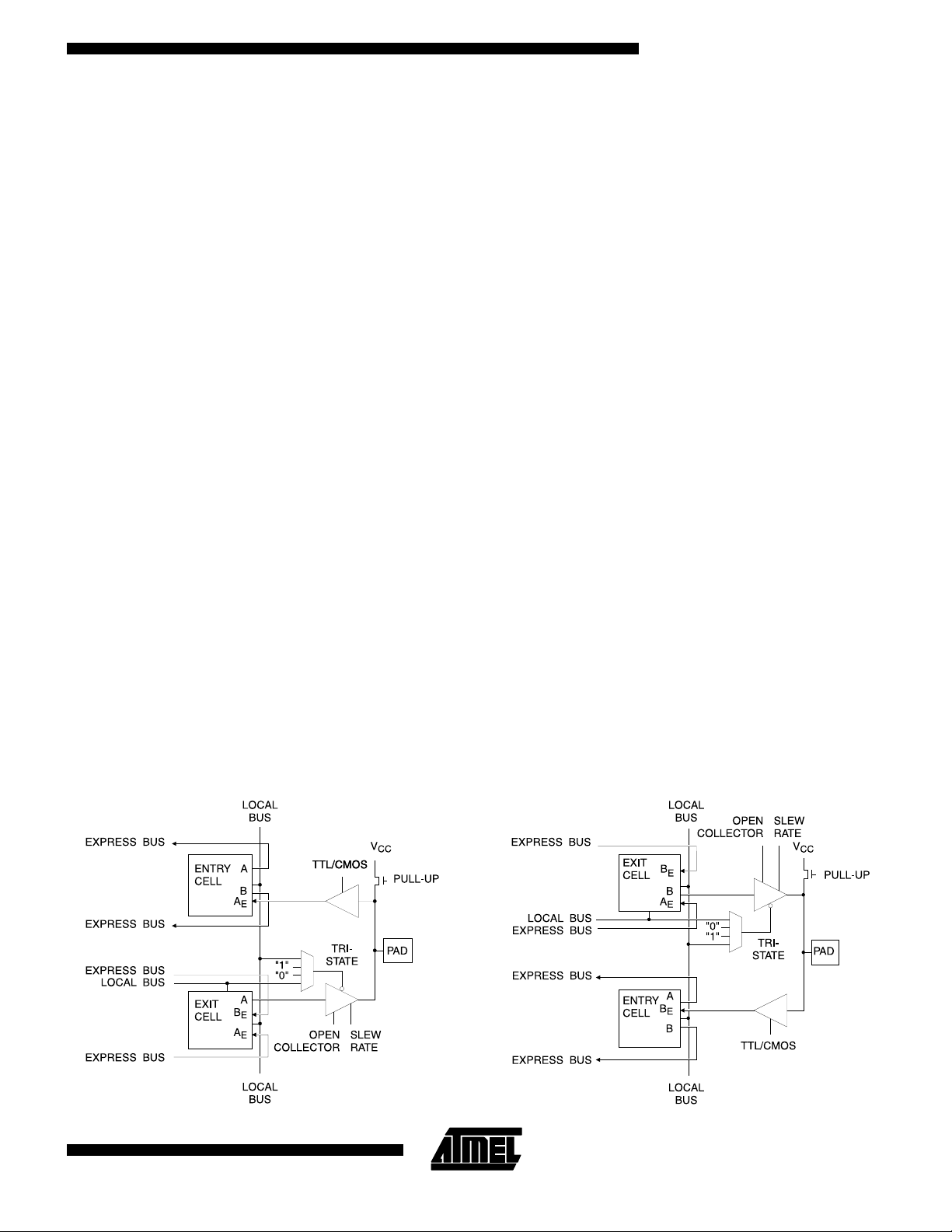
Input/Output
The Atme l architecture pr ovides a flexi ble interface between the logic array, t he configuration cont rol logic and
the I/O pins.
Two adjacent cells— an “exit” and an “entrance” cell— on
the perimeter of the logic array are associated with each
I/O p in .
There are two types of I/Os: A-type (Figure 8a) and B-type
(Figure 8b). For A-type I/Os, the edge-facing A output of
an exit cell is connected to an output driver, and the edgefacing A input of the adj acent entrance cell i s connected to
an input buffer . The output of t he output driver and t he
input of the input buffer are connected to a common pin.
B-type I/Os are the same as A -type I/Os, but use the B
inputs and outputs of their respective entrance and exit
cells. A- and B-type I/ Os alter nate around the array.
Control of the I/O logic is provided by user- confi gurable
me mo ry b it s .
TTL/CMOS Inputs
A user-configurable bit det erm ines the threshold level—
TTL or CMOS— of t he input buffer.
Open Collector/Tri-state Outputs
A user-configurable bit which enables or disables the active pull-up of the output device.
Slew Rate Control
A user- configurabl e bit controls th e slew rat e— fast or
slow— of the output buffer . A slow slew rate, which reduces noise and ground bounce, is recommended for out-
puts that are not speed-critical. Fast and slow slew rates
have the sam e DC-curr ent sinki ng capabil it ies, but th e
rate at whi ch each allows the output devices to reach full
drive differs.
Pull-up
A user-configurable bit controls the pul l-up t ransistor i n the
I/O pin. It’s primary functi on is to provide a logical “1" t o
unused input pins. When on, it is approximately equivalent
to a 25K resistor to VCC.
Enable Select
User-configurable bits determine the output-enable for the
output driver. The output driver can be static - - always on
or always off - - or dynamically controlled by a signal generated i n the array. Four options ar e available from the
array: (1) the control is l ow and always dr iving; (2) the control is high and n ever d riving; (3) the control i s connect ed
to a vertical local bus associated with the output cell; or (4)
the control is connected to a horizontal local bus associated with the output cell. On power-up, the user I/Os are
configured as inputs with pull-up resistors.
In addition to the functionality provided by the I/O logic, the
entrance and exit cell s pr ovide the abil ity t o r egist er bot h
inputs and outputs. Also, t hese perimeter cells (u nlike interior cells) are conn ected directly to express buses: t he
edge-facing A and B outputs of the entrance cell are connected to express buses , as are the edge-facing A and B
inputs of the exit cell. These buse s are per pendicular to
the edge, and provide a rapid means of bringing I /O signals to and from the array interior and the opposite ed ge
of the chip.
Figure 8a. A-Type I/O Logic
Figure 8b. B-Type I/O Logic
2-9

Chip Configuration
The Integrated Devel opment Sy st em generates the
SRAM bit pattern required to conf igure a AT6000 Series
device. A PC parallel port, microprocessor, EPROM or serial configuration memory can be used to download configuration patterns.
Users select from several configuration modes. Many factors, inclu ding board ar ea, configurat ion speed and the
number of designs implemented in parallel can influence
the user’s final choice.
Configuration is controlled by dedicated configuration pins
and dual-function pins that double as I/O pins when the
device is in operation. The number of dual-function pins
required for each mode varies.
The devices can be parti ally reconfigured while in o peration. Portions of the device not being modified remain operational during reconfiguration . Simultaneous configuration of more than one device is also possible. Full configuration takes as little as a millisecond, partial configurat ion
is even faster.
Refer to the Pin Function Description section following for
a brief summary of the pins used in configuration. For
more information about configuration, refer to the AT6000
Series Configuration data sheet.
Pin Function Description
This section provides abbreviated descriptions of the various AT6000 Series pins. For more complete descriptions,
refer to the AT6000 Series Configuration data sheet.
Pinout tables for the AT6000 series of devices follow.
Power Pins
VCC, VDD, GND, V
VCC and GND are the I/O supply pins, VDD and VSS are
the internal logic supply pins. VCC and VDD shoul d be tied
to the same tra ce on the printed circuit board. GND and
VSS should be tied to the same trace on the printed circuit
board.
Input/Output Pins
All I/O pins can be used in the same way (refer to the I/O
section of the architecture description). Some I/O pins are
dual-function pins used during configuration of the array.
When not being used for configuration, dual-functi on I/Os
are fully functional as normal I/O pins. On initial power-up,
all I/Os are conf igured as TTL inputs with a pull-up.
Dedicat ed Timing and Control Pins
CON
Configuration-in-process pin. After power-up, CON staysLow until power-up initialization is complete, at which time
SS
CON is then released. CON is an open collector signal.
After power-up initialization, forcing CON low begins t he
configuration process.
CS
Configuration enable pin. All configuration pins are ignored if CS is high. CS mu st be held low throughout the
configuration process. CS is a TTL input pin.
M0, M1, M2
Configuratio n mode pins are used to determine the configuration mode. All three are TTL input pins.
CCLK
Configuratio n clock pin. C CLK is a TTL input or a CMOS
output dependin g on the mode of opera tion . In modes 1,
2, 3, and 6 it is an input. In modes 4 and 5 it is an output
with a typical frequency of 1 MHz. In all modes, the rising
edge o f the CCLK signal is used to sample in puts a nd
change outputs.
CLOCK
External logic source used to drive the internal global
clock line. Registers toggle on the rising edge of CLOCK.
The CLOCK signal is neither used nor affected by t he configuration modes. It is always a TTL input .
RESET
Array register asynchronous reset. RESET drives the internal global reset. The RESET signal is neither used nor
affected b y the configuration modes. It is always a TT L
input.
Dual-Function Pins
When CON is high, dual-funct ion I/ O pins act as device
I/Os; w hen CON is low, d ual-function pi ns are used as
configuration control or data signals as determined by the
con figura tion modes. C are mu st be ta ken w hen us ing
these pins to ensu re t hat configuration activity does not
interfere with other circuitry connected to these pins in the
application.
D0 or I/O
Serial configuration modes use D0 as the serial data input
pin. Parallel configuration modes use D0 as the least-significant bit. Input data must meet setup and hold r equirements with respect to the rising edge of CCLK. D0 is a TTL
input during configuration.
D1 to D7 or I/O
Parallel configuration modes use these pins as inputs. Serial configuration modes do not use them. Data must meet
set up and ho ld requ iremen ts with respect t o the ri sing
edge of CCLK. D1-D7 are TTL inputs during configuration.
(continued)
2-10
AT6000/LV Series

AT6000/LV Series
Pin Function Description
A0 to A16 or I/O
During configuration in modes 1, 2 and 5, these pins are
CMOS outputs and act as the address pins for a par allel
EPROM. A0-A16 eliminates the need for an external address counter when usi ng an ext ern al parall el nonvolatile
memory to configure the FPGA. Addresses change after
the rising edge of the CCLK signal.
CSOUT or I/O
When cascading devices, CSOUT is an out put used to enable other devices. CSOUT should be connected to the
CS input of the downstream device. The CSOUT function
is optional and can be disabled during initial programming
when casc ading is not us ed. When casca ding devices,
CSOUT should be dedicated to configuration and not used
as a configurable I/O.
CHECK or I/O
During configuration, CHECK is a TTL i nput that can be
used to enable the data check function at the beginning of
a configuration cycle. No data is written to t he device w hile
CHECK is low. Instead, the configuration file being applied
(Continued)
to D0 ( or D0-D7, in parallel m ode) is compared w ith the
cur rent conten ts of the i nternal configu ration RAM. I f a
mismatch is detected between the data being loaded and
the d ata already in the RAM, th e ERR pin goes low. The
CHECK funct ion is optional and can be disabled d uring
initial programming.
ERR or I/O
During configuration, ERR is an output. When the CHECK
function is activated and a mismatch is detected between
the current configuration data stream and the data already
loaded in the configuration RAM, ERR goes low . The ERR
output is a registered signal. O nce a mismatch is found,
the signal is set and is only reset after the configuration
cycle is restarted. ERR is also asserted for configuration
file errors. The ERR f unction is optional and can be disabled during initial programming.
Device Pinout Selection (Max. Number of User I/O)
AT6002 AT6003 AT6005 AT6010
84 PLCC
100 VQFP
132 PQFP
144 TQFP
208 PQFP
240 PQFP
64 I/O 64 I/O 64 I/O —
80 I/O 80 I/O 80 I/O —
96 I/O 108 I/O 108 I/O 108 I/O
96 I/O 120 I/O 108 I/O 120 I/O
— — — 172 I/O
— — — 204 I/O
Bit-Stream Sizes
Mode(s) Type
1 P Preamble 2677 4153 8077 16393
2 P Preamble 2677 4153 8077 16393
3 S Null Byte/Preamble 2678 4154 8078 16394
4 S Null Byte/Preamble 2678 4154 8078 16394
5 P Preamble 2677 4153 8077 16393
6 P Preamble/Preamb le 2678 4154 8078 16394
(1, 2)
Beginning Sequ ence AT6002 AT6003 AT6005 AT6010
Notes: 1. P = Parallel.
2. S = Serial.
2-11

Pinout Assignment
Left Side (Top to Bottom)
84 100 132 144 180 208 240
AT6002 AT6003 AT6005 AT6010
— — — I/O51(A) ————B1 1 1
I/O24(A) or A7 I/O30(A) or A7 I/O27(A) or A7 I/O50(A) or A7 12 1 18 1 C1 2 2
— I/O29(B) — I/O49(A) ———2 D1 3 3
— — — I/O48(B) ————— —4
———VCC————PWR
— — — I/O47(A) ————E1 5 6
———GND————GND
— I/O28(A) I/O26(A) I/O46(A) — — 19 3 G1 7 8
I/O23(A) or A6 I/O27(A) or A6 I/O25(A) or A6 I/O45(A) or A6 13 2 20 4 H1 8 9
— — — I/O44(B) ————— —10
— — — I/O43(A) ————C2 9 11
I/O22(B) I/O26(A) I/O24(A) I/O42(A) — — 21 5 D2 10 1 2
I/O21(A) or A5 I/O25(A) or A5 I/O23(A) or A5 I/O41(A) or A5 14 3 22 6 E2 11 13
— — — I/O40(B) ————— —14
— — — I/O39(A) ————F2 1215
I/O20(B) I/O24(B) I/O22(A) I/O38(A) — 4 23 7 G2 13 16
I/O19(A) or A4 I/O23(A) or A4 I/O21(A) or A4 I/O37(A) or A4 15 5 24 8 H2 14 17
— — — I/O36(B) ————— —18
I/O18(B) I/O22(B) I/O20(A) I/O35(A) — — 25 9 D3 15 1 9
I/O17(A) or A3 I/O21(A) or A3 I/O19(A) or A3 I/O34(A) or A3 16 6 26 10 E3 16 20
I/O16(B) I/O20(B) I/O18(A) I/O33(A) — 7 27 11 F3 1 7 21
— — — I/O32(B) ————— 1822
I/O15(A) or A2 I/O19(A) or A2 I/O17(A) or A2 I/O31(A) or A2 17 8 28 12 G3 19 2 3
— I/O18(B) I/O16(A) I/O30(A) — — 29 13 H3 20 24
GND GND GND GND 18 9 30 14 GND
VSS VSS VSS VSS 19 10 31 15 GND
I/O14(A) or A1 I/O17(A) or A1 I/O15(A) or A1 I/O29(A) or A1 20 11 32 16 F4 23 2 7
— — — I/O28(B) ————— 2428
— I/O16(B) — I/O27(A) ———17G4 2529
I/O13(A) or A0 I/O15(A) or A0 I/O14(A) or A0 I/O26(A) or A0 21 12 33 18 H4 26 30
I/O12(B) or D7 I/O14(A) or D7 I/O13(A) or D7 I/O25(A) or D7 22 13 34 19 H5 27 31
— — — I/O24(B) ————— 2832
I/O11(A) or D6 I/O13(A) or D6 I/O12(A) or D6 I/O23(A) or D6 23 14 35 20 J4 29 33
I/O10(A) or D5 I/O12(A ) or D5 I/O11(A) or D5 I/O22(A) or D5 24 15 36 21 K4 30 34
VDD VDD VDD VDD 25 16 37 22 PWR
VCC VCC VCC VCC 26 17 38 23 PWR
I/O9(B) I/O11(B) I/O10(A) I/O21(A) — — 39 24 J3 33 37
— — — I/O20(B) ————— 3438
I/O8(A) or D4 I/O10(A) or D4 I/O9(A) or D4 I/O19(A) or D4 27 18 40 25 K3 35 39
I/O7(B) I/O9(B) I/O8(A) I/O18(A) — 19 41 26 L3 36 40
— — — I/O17(A) ————M3 3741
— — — I/O16(B) ————— —42
I/O6(A) or D3 I/O8(A) or D3 I/O7(A) or D3 I/O15(A) or D3 28 20 42 27 N3 38 43
— I/07(B) I/O6(A) I/014( A) — — 43 28 J2 39 44
— — — I/O13(A) ————K2 4045
GND GND GND GND — — 44 29 GND
———VSS————GND
— — — I/O12(B) ————— —48
I/O5(A) or D2 I/O6(A) or D2 I/O5(A) or D2 I/O11(A) or D2 29 21 45 30 M2 43 4 9
I/O4(B) I/O5(B) I/O4(A) I/O10(A) — 22 46 31 N2 44 50
PLCC VQFP PQFP TQFP CPGA PQFP PQFP
(1)
45
(2)
67
(2)
21 25
(2)
22 26
(1)
31 35
(1)
32 36
(2)
41 46
(2)
42 47
2-12
(continued)
AT6000/LV Series

AT6000/LV Series
Pinout Assignment
(Continued)
Left Side (Top to Bottom ) (Continued)
84 100 132 144 180 208 240
AT6002 AT6003 AT6005 AT6010
— — — I/O9(A) ————P2 4551
— — — I/O8(B) ————— —52
I/O3(A) or D1 I/O4(A) or D1 I/O3(A) or D1 I/O7(A) or D1 30 23 47 32 J1 46 53
I/O2(B) I/O3(A) I/O2(A) I/O6(A) — — 48 33 K1 47 54
— — — I/O5(A) ————L1 4855
— — — I/O4(B) ————— —56
— I/O2(B) — I/O3(A) ———34M1 4957
I/O1(A) or D0 I/O1(A) or D0 I/O1(A) or D0 I/O2(A) or D0 31 24 49 35 N1 50 58
— — — I/O1(A) ————P1 5159
CCLK CCLK CCLK CCLK 32 25 50 36 R1 52 60
PLCC VQFP PQFP TQFP CPGA PQFP PQFP
Notes: 1. PWR = Pins connected to power plane = F1, E4/E5, L2, R4, K15, L12, E14, A12.
2. GND = Pins connected to ground plane = L4, M4, N9, N10, E12, D12, C7, C6.
Bottom Side (L eft to Right)
84 100 132 144 180 208 240
AT6002 AT6003 AT6005 AT6010
CON CON CON CON 33265137M5 5361
— — — I/O204(A) ————M6 5462
I/O96(A) I/O120(A) I/O108(A) I/O203(A) 34 27 52 38 M7 55 63
— I/O119(B) — I/O202(A) ———39R2 5664
— — — I/O201(B) ————— —65
———VCC————PWR
— — — I/O200(A) ————R3 5867
———GND————GND
— I/O118(A) I/O107(A) I/O199(A) — — 53 40 R5 60 69
I/O95(A) or
— — — I/O197(B) ————— —71
— — — I/O196(A) ————R7 6272
I/O94(B) I/O116(A) I/O105(A) I/O195(A) — — 55 42 P3 63 73
I/O93(A) I/O115(A) I/O104(A) I/O194(A) 36 29 56 43 P4 64 74
— — — I/O193(B) ————— —75
— — — I/O192(A) ————P5 6576
I/O92(B) I/O114(B) I/O103(A) I/O191(A) — 30 57 44 P6 66 77
I/O91(A) or
— — — I/O189(B) ————— —79
I/O90(B) I/O112(B) I/O101(A) I/O188(A) — — 59 46 N4 68 80
I/O89(A) or
I/O88(B) I/O110(B) I/O99(A) I/O186( A) — 33 61 48 N6 70 82
— — — I/O185(B) ————— 7183
I/O87(A) I/O109(A) I/O98(A) I/O184(A) 39 34 62 49 N7 72 84
GND GND GND GND 40 35 64 51 GND
I/O86(A) I/O107(A) I/O96(A) I/O182(A) 41 36 65 52 M9 75 87
— — — I/O181(B) ————— 7688
— I/O106(B) — I/O180(A) ———53M107789
I/O85(A) I/O105(A) I/O95(A) I/O179(A) 42 37 66 54 M11 78 90
CS CS CS CS 43 38 67 55 L8 79 91
I/O84(B) I/O104(A) I/O94(A) I/O178(A) 44 39 68 56 M12 80 92
CSOUT I/O117(A) or CSO UT I/O106( A) or CSOUT I/O1 98(A) or CSOUT35285441R6 6170
CHECK I/O113(A) or CHECK I/O102(A) or CHECK I/O190(A) or CHECK 37 31 58 45 P7 67 78
ERR I/O111(A) or ERR I/O100(A) or ERR I/O187(A) or ERR38326047N5 6981
I/O108(B) I/O97(A) I/O183(A) 63 50 M8 73 85
PLCC VQFP PQFP TQFP CPGA PQFP PQFP
(1)
57 66
(2)
59 68
(2)
74 86
(continued)
2-13

Pinout Assignment
(Continued)
Bottom Side (Left to Right)
(Continued)
84 100 132 144 180 208 240
AT6002 AT6003 AT6005 AT6010
— — — I/O177(B) ————— 8193
I/O83(A) I/O103(A) I/O93(A) I/O176(A) 45 40 69 57 N8 82 94
———VDD————PWR
VCC VCC VCC VCC 46 41 70 58 PWR
I/O82(A) I/O102(A) I/O92(A) I/O175(A) 47 42 71 59 N11 85 97
I/O81(B) I/O101(B) I/O91(A) I/O174(A) — — 72 60 N12 86 98
— — — I/O173(B) ————— 8799
I/O80(A) I/O100(A) I/O90(A) I/O172(A) 48 43 73 61 N13 88 100
I/O79(B) I/O99(B) I/O89(A) I/O171(A) — 44 74 62 P8 89 101
— — — I/O170(A) ————P9 90102
— — — I/O169(B) ————— —103
I/O78(A) I/O98(A) I/O88(A) I/O168(A) 49 45 75 63 P10 91 104
— I/O97(B) I/O87(A) I/O167(A) — — 76 64 P11 92 105
— — — I/O166(A) ————P1293106
GND GND GND GND — — 77 65 GND
— — — I/O165(B) ————— —108
I/O77(A) I/O96(A) I/O86(A) I/O164(A) 50 46 78 66 P13 95 109
I/O76(B) I/O95(B) I/O85(A) I/O163(A) — 47 79 67 P14 96 110
— — — I/O162(A) ————R8 97111
— — — I/O161(B) ————— —112
I/O75(A) I/O94(A) I/O84(A) I/O160(A) 51 48 80 68 R9 98 113
I/O74(B) I/O93(A) I/O83(A) I/O159(A) — — 81 69 R10 99 114
— — — I/O158(A) ————R11100115
— — — I/O157(B) ————— —116
— I/O92(B) — I/O156(A) ———70R12101117
I/O73(A) I/O91(A) I/O82(A) I/O155(A) 52 49 82 71 R13 102 118
— — — I/O154(A) ————R14103119
RESET RESET RESET RESET 53 50 83 72 R15 104 120
PLCC VQFP PQFP TQFP CPGA PQFP PQFP
(1)
83 95
(1)
84 96
(2)
94 107
Notes: 1. PWR = Pins connected to power plane = F1, E4/E5, L2, R4, K15, L12, E14, A12.
2. GND = Pins connected to ground plane = L4, M4, N9, N10, E12, D12, C7, C6.
Right Side (Bottom to Top)
84 100 132 144 180 208 240
AT6002 AT6003 AT6005 AT6010
— — — I/O153(A) ————P15105121
I/O72(A) I/O90(A) I/O81(A) I/O152(A) 54 51 84 73 N15 1 06 122
— I/O89(B) I/O80(A) I/O151(A) — — 85
— — — I/O150(B) ————— —124
———VCC————PWR
— — — I/O149(A) ————L15109126
———GND————GND
— I/O88(A) — I/O148(A) — — 8 5
I/O71(A) I/O87(A) I/O79(A) I/O1 47(A) 55 52 86 76 H15 112 129
— — — I/O146(B) ————— —130
— — — I/O145(A) ————N14113131
I/O70(B) I/O86(A) I/O78(A) I/O1 44(A) — — 87 77 M14 114 132
I/O69(A) I/O85(A) I/O77(A) I/O1 43(A) 56 53 88 78 L14 115 133
— — — I/O142(B) ————— —134
PLCC VQFP PQFP TQFP CPGA PQFP PQFP
(3)
74 M15 107 123
(1)
108 125
(2)
(4)
75 J15 111 128
110 127
(continued)
2-14
AT6000/LV Series

AT6000/LV Series
Pinout Assignment
(Continued)
Right Side (Bottom to Top)
(Continued)
84 100 132 144 180 208 240
AT6002 AT6003 AT6005 AT6010
— — — I/O141(A) ————K14116135
I/O68(B) I/O84(B) I/O76(A) I/O1 40(A) — 54 89 79 J14 117 136
I/O67(A) I/O83(A) I/O75(A) I/O1 39(A) 57 55 90 80 H14 118 137
— — — I/O138(B) ————— —138
I/O66(B) I/O82(B) I/O74(A) I/O1 37(A) — — 91 81 M13 119 139
I/O65(A) I/O81(A) I/O73(A) I/O1 36(A) 58 56 92 82 L13 120 1 4 0
I/O64(B) I/O80(B) I/O72(A) I/O1 35(A) — 57 93 83 K13 121 1 4 1
— — — I/O134(B) ————— 122142
I/O63(A) I/O79(A) I/O71(A) I/O1 33(A) 59 58 94 84 J13 123 143
— I/O78(B) I/O70(A) I/O132( A) — — 95 85 H13 124 144
GND GND GND GND 60 59 96 86 GND
VSS VSS VSS VSS 61 60 97 87 GND
I/O62(A) I/O77(A) I/O69(A) I/O1 31(A) 62 61 98 88 K12 127 147
— — — I/O130(B) ————— 128148
— I/O76(B) — I/O129(A) ———89J12 129149
I/O61(A) I/O75(A) I/O68(A) I/O1 28(A) 63 62 99 90 H12 130 150
I/O60(B) I/O74(A) I/O67(A) I/O1 27(A) 64 63 100 91 H11 131 151
— — — I/O126(B) ————— 132152
I/O59(A) I/O73(A) I/O66(A) I/O1 25(A) 65 64 101 92 G12 133 153
I/O58(A) I/O72(A) I/O65(A) I/O1 24(A) 66 65 102 93 F12 1 3 4 154
VDD VDD VDD VDD 67 66 103 94 PWR
VCC VCC VCC VCC 68 67 104 95 PWR
I/O57(B) I/O71(B) I/O64(A) I/O1 23(A) — — 105 96 G13 137 157
— — — I/O122(B) ————— 138158
I/O56(A) I/O70(A) I/O63(A) I/O1 21(A) 69 68 106 97 F13 1 3 9 159
I/O55(B) I/O69(B) I/O62(A) I/O1 20(A) — 69 107 98 E13 140 160
— — — I/O119(A) ————D13141161
— — — I/O118(B) — — — — — 162
I/O54(A) I/O68(A) I/O61(A) I/O1 17(A) 70 70 108 99 C13 142 163
— I/O67(B) I/O60(A) I/O116( A) — — 109 100 G14 143 164
— — — I/O115(A) ————F14144165
GND GND GND GND — — 110 101 GND
———VSS————GND
— — — I/O114(B) ————— —168
I/O53(A) I/O66(A) I/O59(A) I/O1 13(A) 71 71 111 102 D14 147 169
I/O52(B) I/O65(B) I/O58(A) I/O1 12(A) — 72 112 103 C14 148 170
— — — I/O111(A) ————B14149171
— — — I/O110(B) ————— —172
I/O51(A) I/O64(A) I/O57(A) I/O1 09(A) 72 73 113 104 G15 15 0 173
I/O50(B) I/O63(A) I/O56(A) I/O1 08(A) — — 114 105 F15 151 174
— — — I/O107(A) ————E15152175
— — — I/O106(B) ————— —176
— I/O62(B) — I/O105(A) ———106D15153177
I/O49(A) I/O61(A) I/O55(A) I/O1 04(A) 73 74 115 107 C15 154 178
— — — I/O103(A) ————B15155179
M2 M2 M2 M2 74 75 116 108 A15 156 180
PLCC VQFP PQFP TQFP CPGA PQFP PQFP
(2)
125 145
(2)
126 146
(1)
135 155
(1)
136 156
(2)
145 166
(2)
146 167
Notes: 1. PWR = Pins connected to power plane = F1, E4/E5, L2, R4, K15, L12, E14, A12.
2. GND = Pins connected to ground plane = L4, M4, N9, N10, E12, D12, C7, C6.
3. 85 = Pin 85 on AT6005.
4. 85 = pin 85 on AT6003 and
AT6010.
2-15

Pinout Assignment
(Continued)
Top Side (Right to Left)
84 100 132 144 180 208 240
AT6002 AT6003 AT6005 AT6010
M1 M1 M1 M1 75 76 117 109 D11 157 181
— — — I/O102(A) ————D10158182
I/O48(A) I/O60(A) I/O54(A) I/O10 1(A) 76 77 118 1 10 D9 159 183
— I/O59(B) — I/O100(A) ———111A14160184
— — — I/O99(B) ————— —185
———VCC————PWR
— — — I/O98(A) ————A13162187
———GND————GND
— I/O58(A) I/O53(A) I/O97 (A) — — 119 112 A11 164 189
I/O47 (A) I/O57( A) I/O52(A) I/O96(A) 7 7 7 8 1 20 113 A10 165 190
— — — I/O95(B) ————— —191
— — — I/O94(A) ————A9 166192
I/O46 (B) I/O56( A) I/O51(A) I/O93(A) — — 121 114 B13 167 193
I/O45 (A) I/O55( A) I/O50(A) I/O92(A) 7 8 7 9 1 22 115 B12 168 194
— — — I/O91(B) ————— —195
— — — I/O90(A) ————B11169196
I/O44 (B) I/O54( B) I/O49(A) I/O89(A) — 80 1 23 116 B10 170 197
I/O43 (A) I/O53( A) I/O48(A) I/O88(A) 7 9 8 1 1 24 117 B9 171 198
— — — I/O87(B) ————— —199
I/O42 (B) I/O52( B) I/O47(A) I/O86(A) — — 125 118 C12 172 200
I/O41 (A) I/O51( A) I/O46(A) I/O85(A) 8 0 8 2 1 26 119 C11 173 201
I/O40 (B) I/O50( B) I/O45(A) I/O84(A) — 83 1 27 120 C10 174 202
— — — I/O83(B) ————— 175203
I/O39 (A) I/O49( A) I/O44(A) I/O82(A) 8 1 8 4 1 28 121 C9 176 204
— I/O48(B) I/O43(A) I/O81 (A) — — 129 122 D8 177 205
GND GND GND GND 82 85 130 123 GND
I/O38 (A) I/O47( A) I/O42(A) I/O80(A) 8 3 8 6 1 31 124 D7 179 207
— — — I/O79(B) ————— 180208
— I/O46(B) — I/O78(A) ———125D6 181209
I/O37(A) or A16 I/O45(A) or A16 I/O41(A) o r A16 I/O77(A) or A1 6 84 87 132 126 D5 182 210
CLOCK CLOCK CLOCK CLOCK 1 88 1 127 E8 183 211
I/O36(B) or A15 I/O44(A) or A15 I/O40(A) o r A15 I/O76(A) or A1 5 2 89 2 128 D4 18 4 212
— — — I/O75(B) ————— 185213
I/O35(A) or A14 I/O43(A) or A14 I/O39(A) o r A14 I/O74(A) or A1 4 3 90 3 129 C8 18 6 214
———VDD————PWR
VCC VCC VCC VCC 4 91 4 130 PWR
I/O34(A) or A13 I/O42(A) or A13 I/O38(A) o r A13 I/O73(A) or A1 3 5 92 5 131 C5 18 9 217
I/O33(B) I/O41(B) I/O37(A) I/O7 2(A) — — 6 132 C4 190 218
— — — I/O71(B) ————— 191219
I/O32(A) or A12 I/O40(A) or A12 I/O36(A) o r A12 I/O70(A) or A1 2 6 93 7 133 C3 19 2 220
I/O31(B) I/O39(B) I/O35(A) I/O6 9(A) — 94 8 134 B8 193 221
— — — I/O68(A) ————B7 194222
— — — I/O67(B) ————— —223
I/O30(A) or A11 I/O38(A) or A11 I/O34(A) o r A11 I/O66(A) or A1 1 7 95 9 135 B6 195 224
— I/O37(B) I/O33(A) I/O65(A) — — 10 136 B5 196 225
— — — I/O64(A) ————B4 197226
GND GND GND GND — — 11 137 GND
— — — I/O63(B) ————— —228
I/O29(A) or A10 I/O36(A) or A10 I/O32(A) o r A10 I/O62(A) or A1 0 8 96 12 138 B3 199 229
PLCC VQFP PQFP TQFP CPGA PQFP PQFP
(1)
161 186
(2)
163 188
(2)
178 206
(1)
187 215
(1)
188 216
(2)
198 227
2-16
(continued)
AT6000/LV Series

AT6000/LV Series
Pinout Assignment
(Continued)
Top Side (Right to Left) (Continued)
84 100 132 144 180 208 240
AT6002 AT6003 AT6005 AT6010
I/O28(B) I/O35(B) I/O31(A) I/O6 1(A) — 97 13 139 B2 200 230
— — — I/O60(A) ————A8 201231
— — — I/O59(B) ————— —232
I/O27(A) or A9 I/O34(A) or A9 I/O30(A) or A9 I/O58(A) or A9 9 98 14 140 A7 202 233
I/O26(B) I/O33(A) I/O29(A) I/O5 7(A) — — 15 141 A6 203 234
— — — I/O56(A) ————A5 204235
— — — I/O55(B) ————— —236
— I/O32(B) — I/O54(A) ———142A4 205237
I/O25(A) or A8 I/O31(A) or A8 I/O28(A) or A8 I/O53(A) or A8 10 99 16 14 3 A3 206 238
—
M0 M0 M0 M0 11 100 17 144 A1 208 240
Notes: 1. PWR = Pins connected to power plane = F1, E4/E5, L2, R4, K15, L12, E14, A12.
2. GND = Pins connected to ground plane = L4, M4, N9, N10, E12, D12, C7, C6.
—
—
I/O52(A) ————A2 207239
PLCC VQFP PQFP TQFP CPGA PQFP PQFP
2-17

AC Timing Characteristics – 5V Operation
Delays are based on fixed load. Loads for each t ype of device are described in the notes. Delays ar e in nanoseconds.
Worst case: Vcc = 4.75V to 5.25V. Temperature = 0°C to 70°C.
Load
Cell Function Parameter From To
Wire
(4)
tPD (ma x )
(4)
A, B , L A, B 1 0.8 1. 2 1.8 ns
NAND tPD (max) A, B, L B 1 1.6 2.2 3.2 ns
XOR tPD (max) A, B, L A 1 1.8 2.4 4.0 ns
AND tPD (max) A, B, L B 1 1.7 2.2 3.2 ns
MUX tPD (ma x )
A, B A 1 1.7 2.3 4.0 ns
L A 1 2.1 3.0 4.9 ns
D-Flip-Flop
D-Flip-Flop
(5)
(5)
t
(min) A, B, L CLK 1.5 2.0 3.0 ns
setup
t
(min) CLK A, B, L 0.0 0.0 0.0 ns
hold
D-Flip-Flop tPD (max) CLK A 1 1.5 2.0 3.0 ns
Bus Driver tPD (max) A L 2 2.0 2.6 4.0 ns
Repeater tPD (ma x )
L, E E 3 1.3 1.6 2.3 ns
L, E L 2 1.7 2.1 3.0 ns
Col u m n Clock tPD (max) GCLK, A, ES CLK 3 1.8 2.4 3 .0 ns
Col u m n Re s et tPD (max) GRES, A, EN RES 3 1.8 2.4 3.0 ns
(1)
(5)
(2)
(3)
(3)
(3, 5)
(3, 5)
(5)
tPD (max) CLOCK PIN GCLK 1.6 2.0 2.9 ns
tPD (ma x ) RESET PIN GRE S 1.5 1.9 2.8 ns
tPD (max) I/O A 3 1.0 1.2 1.5 ns
tPD (max) I/O A 3 1.3 1.4 2.3 ns
tPD (ma x ) A I/O P IN 4 3.3 3.5 6. 0 ns
tPD (max) A I/O PIN 4 7.5 8. 0 12. 0 ns
(5 )
t
(max) L I/O PIN 4 3.1 3.3 5.5 ns
PXZ
t
(max) L I/O PIN 4 3.8 4.0 6.5 ns
PZX
t
(max) L I/O PIN 4 8.2 8.5 12.5 ns
PZX
Clock Buffer
Reset Buffer
TTL Input
CMOS Input
Fas t Ou tp u t
Slow Output
Output Disable
Fast Enable
Slow Enable
Defini tion - 1 - 2 - 4 Units
Device Cell Types Outputs Icc (max)
(6)
Cell
(6)
Bus
Col u m n Clock
Notes:
1. TTL buffer delays are measured from a V
of 1.5V at the pad to the internal VIH at A.
The input buffer load is constant.
2. CMOS buffer delays are measured from a
V
of 1/2 VCC at the pad to the internal
IH
V
at A. The input buffer load is constant.
IH
3. Buffer delay is to a pad voltage of 1.5V
with one output switching.
2-18
(6)
AT6000/LV Series
Wire, XWire, Half-Adder, Flip-Flop A, B 4.5 µA/MHz
Wire, XWire, Half-Adder, Flip-Flop, Repeater L 2.5 µA/MHz
Column Clock Driver CLK 40 µA/MHz
4. Max specifications are the average of max
IH
t
and t
PDLH
5. Parameter based on characterization and
simulation; not tested in production.
6. Exact power calculation is available in an
Atmel application note.
PDHL
.
Load Definition:
1. Load of one A or B input
2. Load of one L input
3. Constant Load
4. Tester Load of 50 pF
= Preliminary Information

AT6000/LV Series
AC Timing Characteristics – 3.3V Operation
Delays are based on fixed load. Loads for each t ype of device are described in the notes. Delays ar e in nanoseconds.
Worst case: Vcc = 3.0V to 3.6V. Temperature = 0°C to 70°C.
Cell Function Parameter From To Load Definition - 4 Units
(4)
Wire
tPD (ma x)
NAND tPD (max) A, B, L B 1 3.2 ns
XOR tPD (max) A, B, L A 1 4.0 ns
AND tPD (max) A, B, L B 1 3.2 ns
MUX tPD (ma x)
D-Flip-Flop
D-Flip-Flop
(5)
(5)
t
setup
t
hold
D-Flip-Flop tPD (max) CLK A 1 3.0 ns
Bus Driver tPD (max) A L 2 4.0 ns
Repeater tPD (ma x)
Col u m n Clock tPD (max) GCLK, A, ES CLK 3 3.0 ns
Col u m n Re s et tPD (max) GRES, A, EN RES 3 3.0 ns
(1)
(5)
(2)
(3)
(3)
(3, 5)
(3, 5)
(5)
tPD (max) CLOCK PIN GCLK 4 2.9 ns
tPD (max) RESET PIN GRES 5 2.8 ns
tPD (max) I/O A 3 1.5 ns
tPD (max) I/O A 3 2.3 ns
tPD (max) A I/O PIN 6 6.0 ns
tPD (max) A I/O PIN 6 12.0 ns
(5 )
t
PXZ
t
PZX
t
PZX
Clock Buffer
Reset Buffer
TTL Input
CMOS Input
Fas t Ou tp u t
Slow Output
Output Disable
Fast Enable
Slow Enable
(4)
A, B, L A, B 1 1.8 ns
A, B A 1 4.0 ns
LA 14.9ns
(min) A, B, L CLK 3.0 ns
(min) CLK A, B, L 0.0 ns
L, E E 3 2.3 ns
L, E L 2 3.0 ns
(ma x ) L I/O PIN 6 5 .5 n s
(ma x ) L I/O PIN 6 6 .5 n s
(max) L I/O PIN 6 12.5 ns
Device Cell Types Outputs Icc (max)
(6)
Cell
(6)
Bus
Col u m n Clock
Notes:
1. TTL buffer delays are measured from a V
pad to the internal V
2. CMOS buffer delays are measured from a V
the pad to the internal V
stant.
3. Buffer delay is to a pad voltage of 1.5V with one output
switching.
4. Max specifications are the average of max t
5. Parameter based on characterization and simulation; not
tested in production.
(6)
Wire, XWire, Half-Adder, Flip-Flop A, B 2.3 µA/MHz
Wire, XWire, Half-Adder, Flip-Flop, Repeater L 1.3 µA/MHz
Column Clock Driver CLK 20 µA/MHz
6. Exact power calculation is available in an Atmel application
of 1.5V at the
IH
at A. The input buffer load is constant.
IH
of 1/2 VCC at
IH
at A. The input buffer load is con-
IH
and t
PDLH
PDHL
.
note.
Load Definition:
1. Load of one A or B input
2. Load of one L input
3. Constant Load
4. Load of 28 Clock Columns
5. Load of 28 Reset Columns
6. Tester Load of 50 pF
2-19

Absolute Maxi mum Ratings *
Supply Voltage (VCC)......................... -0.5V to +7.0V
DC Input Voltage (VIN)...............-0.5V to VCC + 0.5V
DC Output Voltage (VON)...........-0.5V to VCC + 0.5V
Storage Temperature Range
(TSTG)............................................-65°C to +150°C
Power Dissipati on (PD)..............................1500 mW
Lead Temperature (TL)
(Soldering, 10 sec.). ....................................... ..260°C
*NOTICE: Stresses beyond those listed under Absolute Maxi-
mum Ratings may cause permanent damage to the device.
These are stress ratings only, and functional operation of
the device at these or any other conditions beyond those
listed under Operating Conditions is not implied. Exposure
to Absolute Maximum Ratings conditions for extended periods of time may affect device reliability.
ESD (R
ZAP
=1.5K , C
=100 pF)....................2000V
ZAP
DC and AC Operating Range – 5V Operation
AT6002-2/4
AT6003-2/4
AT6005-2/4
AT6010-2/4
Commercial
Operating Temperature (Case) 0°C - 70°C -40°C - 85°C -55°C - 125°C
VCC Power Supply 5V ± 5% 5V ± 10% 5V ± 10%
Input Voltage Level
(TTL)
Input Voltage Level
(CMOS)
High (V
Low (V
High (V
Low (V
)2.0V - VCC2. 0V - V
IHT
) 0V - 0.8V 0V - 0.8V 0V - 0.8V
ILT
) 70% - 100% V
IHC
) 0 - 30% V
ILC
CC
CC
Input Signal Transition Time (TIN) 50 ns (max) 50 ns (max) 50 ns (max)
AT6002-2/ 4
AT6003-2/ 4
AT6005-2/ 4
AT6010-2/ 4
Industrial
CC
70% - 100% V
CC
AT6002-4
AT6003-4
AT6005-4
AT6010-4
Military
2.0V - V
70% - 100% V
0 - 30% VCC 0 - 30% V
DC and AC Operating Range – 3.3V Operation
AT6002-4, AT6003-4
AT6005-4, AT6010-4
Commercial
Operating Temperature (Case) 0°C - 70°C
VCC Power Supply 3.3V ± 10%
Input Voltage Level
(TTL)
Input Voltage Level
(CMOS)
High (V
Low (V
High (V
Low (V
Input Signal Transition Time (TIN) 50 ns (max)
)2.0V - V
IHT
)0V - 0.8V
ILT
) 70% - 100% V
IHC
)0 - 30% V
ILC
CC
CC
CC
CC
CC
CC
2-20
AT6000/LV Series

AT6000/LV Series
DC Characteristics – 5V Operation
Symbol Parameter Conditions Min Max Units
V
V
V
V
I
OZH
I
OZL
I
IH
I
IL
I
CC
C
IH
IL
OH
OL
IN
High-Level Input Voltage Commercial
CMOS 70% V
CC
TTL 2.0 V
Low-Level Input Voltage Commercial
CMOS 0 30% V
TTL 0 0.8 V
High-Level Output
Voltage
Commercial
Low-Level Output Voltage Commercial
IOH = -4 mA, VCC min 3.9 V
IOH = -16 mA, VCC min 3.0 V
IOL = 4 mA, VCC min 0.4 V
IOL = 16 mA, VCC min 0.5 V
High-Level Tristate
Output Leakage Current
Low-Level Tristate Without Pull-Up, VO = V
Output Leakage Current With Pull-Up, VO = V
VO = VCC (ma x ) 10 µA
SS
SS
-10 µA
-500 µA
High-Level Input Current VIN = VCC (ma x) 10 µA
Low-Level Input Current
Without Pull-Up, VIN = V
With Pull-Up, VIN = V
SS
SS
-10 µA
-500 µA
Power Consumption Without Internal Oscillator (Standby) 500 µA
Input Capacitance All Pins 10 pF
V
CC
CC
CC
V
V
V
2-21

DC Characteristics – 3.3V Operation
Symbol Parameter Conditions Min Max Units
V
V
V
V
I
OZH
I
OZL
I
IH
I
IL
I
CC
C
IH
IL
OH
OL
IN
(1)
High-Level Input Voltage Commercial
CMOS 70% V
CC
TTL 2.0 V
Low-Level Input Voltage Commercial
CMOS 0 30% V
TTL 0 0.8 V
High-Level Output
Voltage
Commercial
Low-Level Output Voltage Commercial
IOH = -2 mA, VCC min 2.4 V
IOH = -6 mA, VCC min 2.0 V
IOL = +2 mA, VCC min 0.4 V
IOL = +6 mA, VCC min 0.5 V
High-Level Tristate
Output Leakage Current
Low-Level Tristate Without Pull-Up, VO = V
Output Leakage Current With Pull-Up, VO = V
VO = VCC (ma x ) 10 µA
SS
SS
-10 µA
-250 µA
High-Level Input Current VIN = VCC (ma x) 10 µA
Low-Level Input Current
Without Pull-Up, VIN = V
With Pull-Up, VIN = V
SS
SS
-10 µA
-250 µA
Power Consumption Without Internal Oscillator (Standby) 200 µA
Input Capacitance All Pins 10 pF
V
CC
CC
CC
V
V
V
Note: 1. Parameter based on characterization and simulation; it is not tested in production.
2-22
AT6000/LV Series

Device Timing: During Operation
AT6000/LV Series
Ordering Information
Usable
Gates
6,000 2 AT 6002-2 AC 100A 5V Commercial
6,000 4 AT 6002-4 AC 100A 5V Commercial
Speed
Ordering Code Package Operation Range
Grade (ns)
AT6002A-2AC 144A (0°C to 70°C)
AT6002-2JC 84J
AT6002-2QC 132Q
AT6002-2AI 100A 5V Industrial
AT6002A-2AI 144A (-40°C to 85°C)
AT6002-2JI 84J
AT6002-2QI 132 Q
AT6002A-4AC 144A (0°C to 70°C)
AT6002-4JC 84J
AT6002-4QC 132Q
AT6002LV-4AC 100A 3.3V Commercial
AT6002ALV-4AC 144A (0°C to 70°C)
AT6002LV-4JC 84J
AT6002LV-4QC 132Q
AT6002-4AI 100A 5V Industrial
AT6002A-4AI 144A (-40°C to 85°C)
AT6002-4JI 84J
AT6002-4QI 132 Q
2-23

Ordering Information
Usable
Gates
9,000 2 AT 6003-2 AC 100A 5V Commercial
9,000 4 AT 6003-4 AC 100A 5V Commercial
Speed
Ordering Code P ackage Operation Range
Grade (ns)
AT6003A-2AC 144A (0°C to 70°C)
AT6003-2JC 84J
AT6003-2QC 132Q
AT6003-2AI 100A Industrial
AT6003A-2AI 144A (-40°C to 85°C)
AT6003-2JI 84J
AT6003-2QI 132 Q
AT6003A-4AC 144A (0°C to 70°C)
AT6003-4JC 84J
AT6003-4QC 132Q
AT6003LV-4AC 100A 3.3V Commercial
AT6003ALV-4AC 144A (0°C to 70°C)
AT6003LV-4JC 84J
AT6003LV-4QC 132Q
AT6003-4AI 100A 5V Industrial
AT6003A-4AI 144A (-40°C to 85°C)
AT6003-4JI 84J
AT6003-4QI 132 Q
Usable
Gates
15,000 2 AT6005-2AC 100A 5V Commercial
15,000 4 AT6005-4AC 100A 5V Commercial
Speed
Ordering Code P ackage Operation Range
Grade (ns)
AT6005A-2AC 144A (0°C to 70°C)
AT6005-2JC 84J
AT6005-2QC 132Q
AT6005A-2QC 208Q
AT6005-2AI 100A Industrial
AT6005A-2AI 144A (-40°C to 85°C)
AT6005-2JI 84J
AT6005-2QI 132 Q
AT6005A-2QI 208Q
AT6005A-4AC 144A (0°C to 70°C)
AT6005-4JC 84J
AT6005-4QC 132Q
AT6005A-4QC 208Q
AT6005LV-4AC 100A 3.3V Commercial
AT6005ALV-4AC 144A (0°C to 70°C)
AT6005LV-4JC 84J
AT6005LV-4QC 132Q
AT6005ALV-4QC 208Q
2-24
AT6000/LV Series

AT6000/LV Series
Ordering Information
Usable
Gates
15,000 4 AT6005-4AI 100 A 5V Industrial
30,000 2 AT6010-2JC 84J 5V Commerci al
30,000 4 AT6010A-4AC 144A 5V Commercial
Speed
Ordering Code P ackage Operation Range
Grade (ns)
AT6005A-4AI 144A (-40°C to 85°C)
AT6005-4JI 84J
AT6005-4QI 132 Q
AT6005A-4QI 208Q
AT6010A-2AC 144A (0°C to 7 0 ° C)
AT6010-2QC 132Q
AT6010A-2QC 208Q
AT6010H-2QC 240Q
AT6010-2JI 84J Industrial
AT6010A-2AI 144A (-40°C to 85°C)
AT6010-2QI 132 Q
AT6010-2QI 208 Q
AT6010-2QI 240 Q
AT6010-4QC 132Q (0°C to 7 0 ° C)
AT6010-4JC 84J
AT6010A-4QC 208Q
AT6010H-4QC 240Q
AT6010ALV-4AC 144A 3.3V Commercial
AT6010LV-4QC 132Q (0°C to 7 0 ° C)
AT6010LV-4JC 84J
AT6010ALV-4QC 208Q
AT6010HLV-4QC 240Q
AT6010A-4AI 144A 5V Industrial
AT6010-4QI 132 Q (-40°C to 85°C)
AT6010-4JI 84J
AT6010A-4QI 208Q
AT6010H-4QI 240Q
Ordering Information
84J
100A
132Q
144A
208Q
240Q
84 Lead, Plastic J-Leaded Chip Carrier (PLCC)
100 Lead, Very Thin (1.0 mm) Plastic Gull Wing Quad Flat Package (VQFP)
132 Lead, Bumpered Plastic Gull Wing Quad Flat Package (BQFP)
144 Lead, Thin (1.4 mm) Plastic Gull Wing Quad Flat Package (TQFP)
208 Lead, Plastic Gull-Wing Quad Flat Package (PQFP)
240 Lead, Plastic Gull-Wing Quad Flat Package (PQFP)
Package Type
2-25
 Loading...