

512K byte
Flash Memory
PCMCIA Card
AT5FC512
Features
Single Power Supply
•
Read and Write Voltage, 5V ± 5%
High Performance
•
200 ns Maximum Ac ce ss Time
6 ms Typical Sector Write
CMOS Low Power Consumption
•
20 mA Typical Active Current (Byte Mode)
400 µA Typical Standby Current
Fully MS-DOS Compatible Flash Driv er an d Fo rmatter
•
Virtual-Disk Flash Driver with 256 Bytes /Se ctor
Random Read/Wri te to an y Sec tor
No Erase Operation Require d Prior to any Write
Zero Data Retention Power
•
Batteries not Required for Data Storage
PCMCIA/JEIDA 68-Pin Standard
•
Selectable Byte- or Word-Wide Configuratio n
High Re-programmabl e Endurance
•
Built-in Redunda nc y for Sec tor Replacement
Minimum 100, 000 Write Cycles
Five Levels of Write Protecti on
•
Prevent Accidental Data Loss
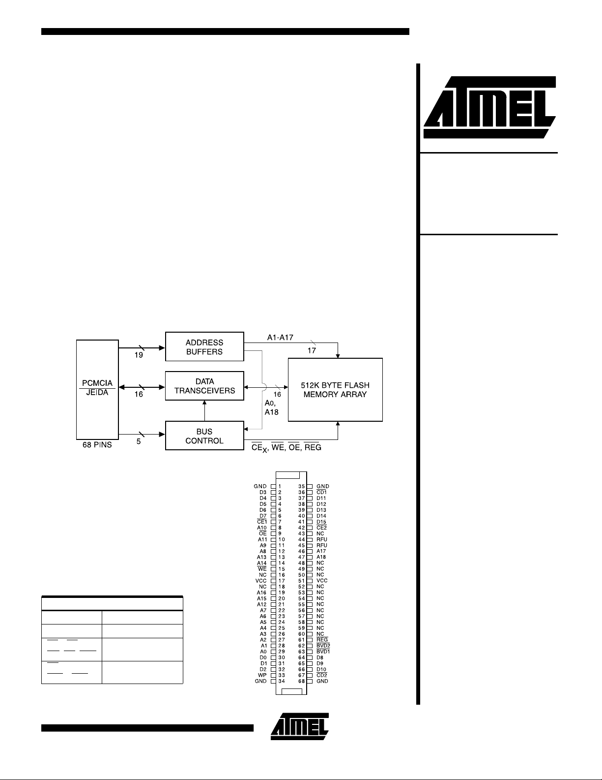
Block Diagram
Pin Configuration
Pin Name Function
A0-A18 Addresses
D0-D15 Data
CE1, CE2,
WE, OE, REG
CD, WP
BVD1, BVD2
Control Signals
Card Status
Description
Atmel’s Flash Memory Card provides the highest system
level performance for data and file storage solutions to the
portable PC market segment. Data files and applications
programs can be stored on the AT5FC512. This allows
OEM manufacturers of portable system to eliminate the
weight, power consumption and reliability issues associated with electro-mechanical disk-based systems. The
AT5FC512 requires a single voltage power supply for total
system operation. No batteries are needed for data retention due to its Flash-based technology. Since no high voltage (12-volt) is required to perform any write operation,
the AT5FC512 is suitable for the emerging "mobile" personal systems.
The AT5FC512 is compatible with the 68-pin
PCMCIA/J EIDA international st andard. Atmel’s Flash
Memory Cards can be read in either a byte-wide or wordwide mode which allows for flexible integration into various
system platforms. It can be read like any typical PCMCIA
SRAM or ROM card.
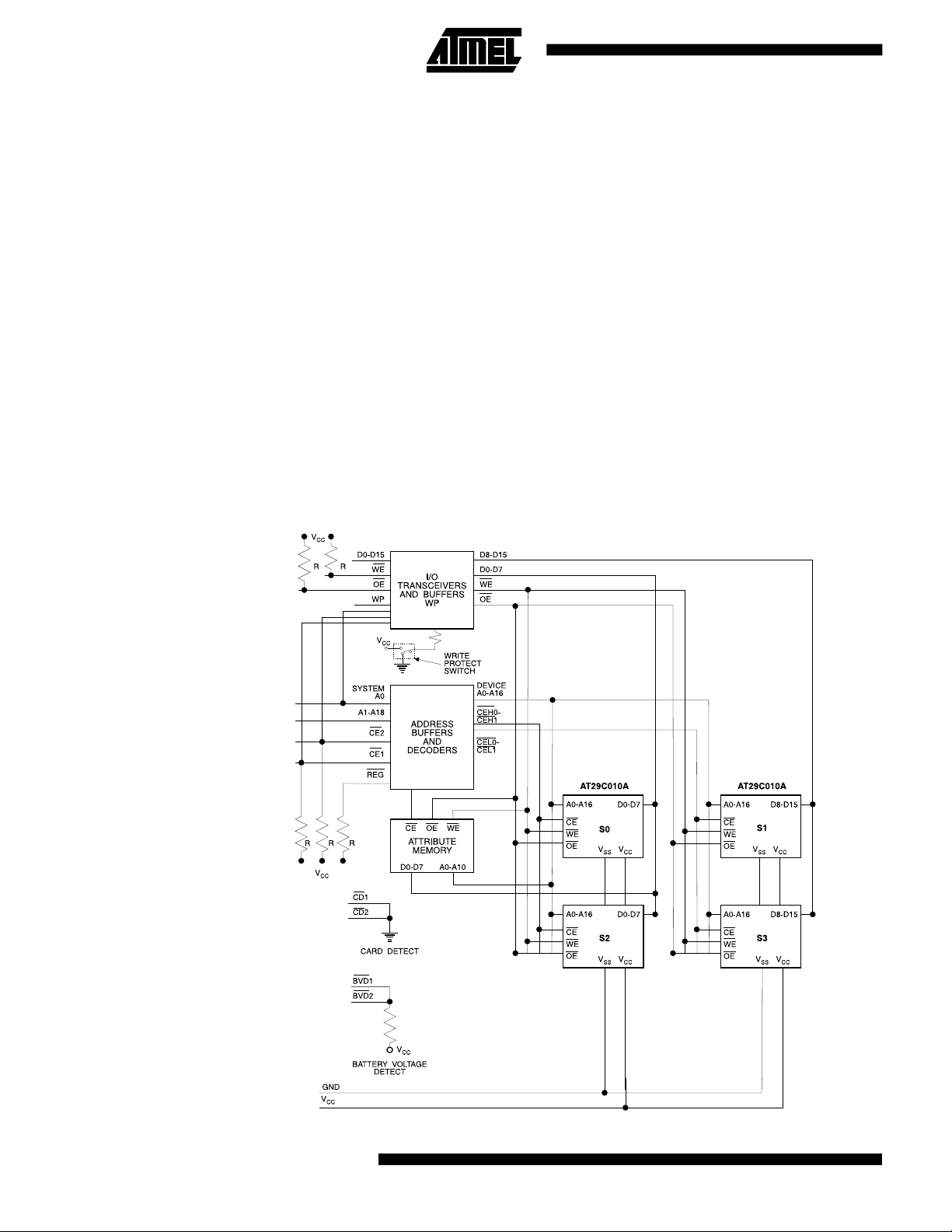
Block Diagram
The Card Information Structure (CIS) can be written by the
OEM or by Atmel at the attribute memory address space
using a format utility. The CIS appears at the beginning of
the card’s attribute memory space and defines the lowlevel organization of data on the PC card. The AT5FC512
contains a separate 2K byte EEPROM memory for the
card’s attribute memory space.
The third party software solutions such as AWARD Software’s CardWare system and the SCM’s Flash File System (FFS), enables Atmel’s Flash Memory Card to emulate the function of essentially all the major brand personal
computers that are DOS/Windows compatible.
For some unique portable computers, such as the
HP200/100/95LX series, the software Driver and Formatter are also available. The Atmel Driver and Formatter utilizes a self-contained spare sector replacement algorithm,
enabled by Atmel’s small 256-byte sectors, to achieve
long term card reliability and endurance.
2 AT5FC512

Absolute Maximum Rat ings*
AT5FC512
Storage Temperature........................ -30°C to +70°C
Ambient Temperature with
Power Applied...................................-10°C to +70°C
Voltage with
Respect to Ground, All pins
(1)
V
................................................ -2.0V to +7.0V
CC
Output Short Circuit Current
(1)
........... -2.0V to +7.0V
(2)
....................-200 mA
*NOTICE: Stresses beyond those listed unde r "Abs olut e Maxi -
mum Ratings" may caus e permanent damage to the card.
This is a stress rating only and functional operation of the
card at these or any other conditions beyond those indicated in the operational sections of this specification is not
implied.Exposure to abso lu te maximum ra ti ng condi ti on s fo r
extended periods may affect device rel iability.
Notes:
1. Minimum DC voltage on input or I/O pins is -0.5V. Durin g
voltage tra ns ients, inputs may oversho ot V
periods of up to 20 ns. Maximum DC voltage on output and
I/O pins is VCC + 0.5V. During voltage transitions, outputs
may overshoot to V
2. No more than one output shorted at a time. Durat io n of the
short circuit should not be greater than one second. Conditions equa l V
OUT
DC and AC Operating Range
Operating Temperature (Case) Com. 0
+ 2.0V for period s up t o 20 ns.
CC
= 0.5V or 5.0V, VCC = Max.
AT5FC512-20
o
C - 70oC
to -2.0V for
SS
Power Supply 5V ± 5%
V
CC
Pin Capacitance
(f = 1 MHz, T = 25°C)
(1)
Symbol Parameter Conditions Typ Max Units
C
IN1
C
OUT
C
IN2
C
I/O
Note: 1. This parameter is charac terized and is not 100% t ested.
Address Capacitance VIN = 0V 20 pF
Output Capacitance V
= 0V 20 pF
OUT
Control Capacitance VIN = 0V 45 pF
I/O Capacitance V
= 0V 20 pF
I/O
3

PC Card Pin Assignments
I = Input, O = Output, I/O = Bi-directional, NC = No Connect
Pin Signal I/O Function
1 GND Ground
2 D3 I/O Data Bit 3
3 D4 I/O Data Bit 4
4 D5 I/O Data Bit 5
5 D6 I/O Data Bit 6
6 D7 I/O Data Bit 7
7
CE
1
I Card Enable 1
8 A10 I Address Bit 10
9
OE I Output Enable
10 A11 I Address Bit 11
11 A9 I Address Bit 9
12 A8 I Address Bit 8
13 A13 I Address Bit 13
14 A14 I Address Bit 14
15
WE I Write Enable
16 NC No Connect
17 V
CC
Power Supply
18 NC No Connect
(1)
Pin Signal I/O Function
35 GND Ground
36
CD
1
O Card Detect 1
37 D11 I/O Data Bit 11
38 D12 I/O Data Bit 12
39 D13 I/O Data Bit 13
40 D14 I/O Data Bit 14
41 D15 I/O Data Bit 15
42
CE
2
I Card Enable 2
43 NC No Connect
44 RFU Reserved
45 RFU Reserved
46 A17 I Address Bit 17
47 A18 I Address Bit 18
48 NC No Connect
49 NC No Connect
50 NC No Connect
51 V
CC
Power Supply
52 NC No Connect
(1)
(1)
19 A16 I Address Bit 16
20 A15 I Address Bit 15
21 A12 I Address Bit 12
22 A7 I Address Bit 7
23 A6 I Address Bit 6
24 A5 I Address Bit 5
25 A4 I Address Bit 4
26 A3 I Address Bit 3
27 A2 I Address Bit 2
28 A1 I Address Bit 1
29 A0 I Address Bit 0
30 D0 I/O Data Bit 0
31 D1 I/O Data Bit 1
32 D2 I/O Data Bit 2
33 WP O Write Protect
(1)
34 GND Ground
Notes: 1. Signal must not be connected between cards.
53 NC No Connect
54 NC No Connect
55 NC No Connect
56 NC No Connect
57 NC No Connect
58 NC No Connect
59 NC No Connect
60 NC No Connect
61
62
63 BVD
REG I Register Select
BVD
O Battery Voltage Detect 2
2
O Battery Voltage Detect 1
1
64 D8 I/O Data Bit 8
65 D9 I/O Data Bit 9
66 D10 I/O Data Bit 10
67
CD
2
O Card Detect 2
68 GND Ground
2. BVD = Internally pulled up.
(2)
(2)
(1)
4 AT5FC512

AT5FC512
Pin Description
Symbol Name Type Function
A0-A18 Address Inputs Input Address Inputs are internally latched during write cycles.
Data Input/Outputs are internally latched on write cycles.
D0-D15 Data Input/Output
CE1, CE
2
Card Enable Input
Input/Output
Data outputs are latched during read cycles. Data pins
are active high. When the memory card is de-selected or
the outputs are disabled the outputs float to tri-state.
Card Enable is active low. The memory card is
de-selected and power consumption is reduced to
standby levels when
memory card circuitry that controls the high and low byte
control logic of the card, input buffers, segment decoders,
and associated memory devices.
CE is high. CE activates the internal
OE Output Enable Input
WE Write Enable Input
V
CC
GND Ground Ground
CD1, CD
WP Write Protect Output
NC No Connect Corresponding pin is not connected internally.
BVD1, BVD
REG Register Select Input
2
PC Card Power
Supply
Card Detect Output
Battery Voltage Detect Output Internally pulled up. (There is no battery in the card.)
2
Memory Card Operations
The AT5FC512 Flash Memory Card is organized as an
array of 4 individual AT29C010A devices. They are logically defined as contiguous sectors of 256 bytes. Each
sector can be read and written randomly as designated by
erase
the host. There is NO need to
write
operation. Also, there is NO high voltage (12V) re-
quired to perform any write operations.
The common memory space data contents are altered in
a similar manner as writing to individual Flash memory devices. On-card address and data buffers activate the appropriate Flash device in the memory array. Each device
internally latches address and data during write cycles.
Refer to the Common Memory Operations table.
any sector prior to any
Output Enable is active low and enables the data buffers
through the card outputs during read cycles.
Write Enable is active low and controls the write function
to the memory array. The target address is latched on the
falling edge of the
latched on the rising edge of the pulse.
PC Card Power Supply for device operation
(5.0V ± 5%)
When Card Detect 1 and 2 = Ground the system detects
the card.
Write Protect is active high and indicates that all card
write operations are disabled by the write protect switch.
Provide access to Card Information Structure in the
Attribute Memory Device
WE pulse and the appropriate data is
Byte-Wide Operations
The AT5FC512 provides the flexibility to operate on data
in byte-wide or word-wide operations. Byte-wide data is
available on D0-D7 for read and write operations (
CE2 = high). Even and odd bytes are stored in a pair
low,
of memory chip segments (i.e., S0 and S1) and are accessed when A0 is low and high respectively.
Word-Wide Operations
The 16 bit words are accessed when both CE1 and CE
are forced low, A0 = don’t care. D0-D15 are used for wordwide operations.
CE1 =
2
(continued)
5
 Loading...