

Features
• 16-Mbit Flash and 2-Mbit/4-Mbit SRAM
• Single 66-ball 8 mm x 10 mm x 1.2 mm CBGA Package
• 2.7V to 3.3V Operating Voltage
Flash
• 2.7V to 3.3V Read/Write
• AccessTime–85ns
• Sector Erase Architecture
– Thirty-one 32K Word (64K Byte) Sectors with Individual Write Lockout
– Eight 4K Word (8K Byte) Sectors with Individual Write Lockout
• Fast Word Program Time – 20 µs
• Fast Sector Erase Time – 300 ms
• Dual-plane Organization, Permitting Concurrent Read While Program/Erase
– Memory Plane A: Eight 4K Word and Seven 32K Word Sectors
– Memory Plane B: Twenty-four 32K Word Sectors
• Erase Suspend Capability
– Supports Reading and Programming from Any Sector by Suspending Erase of a
Different Sector
– Supports Reading Any Word by Suspending Programming of Any Other Word
• Low-power Operation
–30mAActive
– 10 µA Standby
• Data Polling, Toggle Bit, Ready/Busy for End of Program Detection
• VPP Pin for Accelerated Program/Erase Operations
• RESET Input for Device Initialization
• Sector Lockdown Support
• Top/Bottom Block Configuration
• 128-bit Protection Register
16-megabit
Flash and
2-megabit/
4-megabit
SRAM Stack
Memory
AT52BR1672(T)
AT52BR1674(T)
SRAM
• 2-megabit (128K x 16)/4-megabit (256K x 16)
• 2.7V to 3.3V V
• 70 ns Access Time
• Fully Static Operation and Tri-state Output
• 1.2V (Min) Data Retention
• Industrial Temperature Range
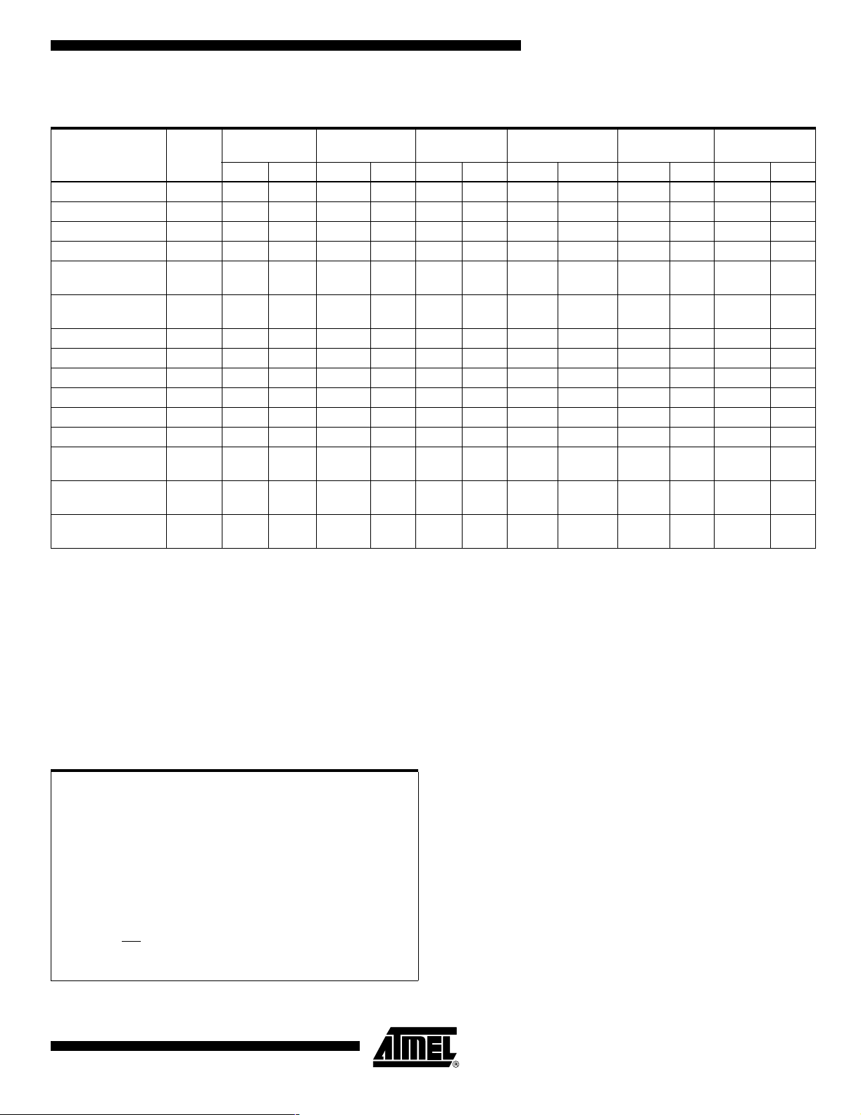
Device Number
AT52BR1672(T) 12M + 4M 16M (1M x 16) 2M (128K x 16)
AT52BR1674(T) 12M + 4M 16M (1M x 16) 4M (256K x 16)
Operating Voltage
CC
Flash Plane
Architecture
Flash
Configuration
SRAM
Configuration
Preliminary
Rev. 2604B–STKD–09/0 2
1
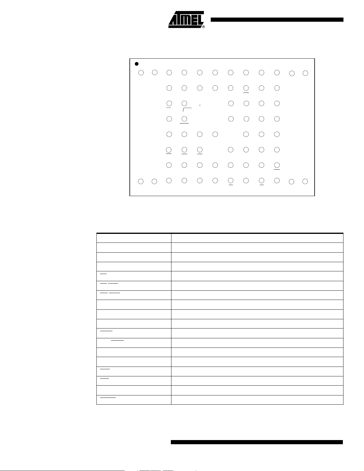
CBGA Top View
1
2
45678910
3
11 12
A
NC
NC
NC
A11
A15
A14
A13
A12
GND
NC
NC
NC
B
A16
A10
A8
I/O15
SWE
I/O14
I/O7
A9
C
I/O13
I/O6
I/O4
WE
RDY BUSY
I/O5
D
I/O12
SCS2
SVcc
SGND
RESET
Vcc
E
NC
Vpp
A19
I/O10
I/O2
I/O3
I/O11
F
SLB
SUB
SOE
I/O9
I/O8
I/O0
I/O1
G
A18
A17
A7
A3
A2
A1
SCS1
A6
H
NC
NC
NC
A0
A4
A5
CE
GND
OE
NC
NC
NC
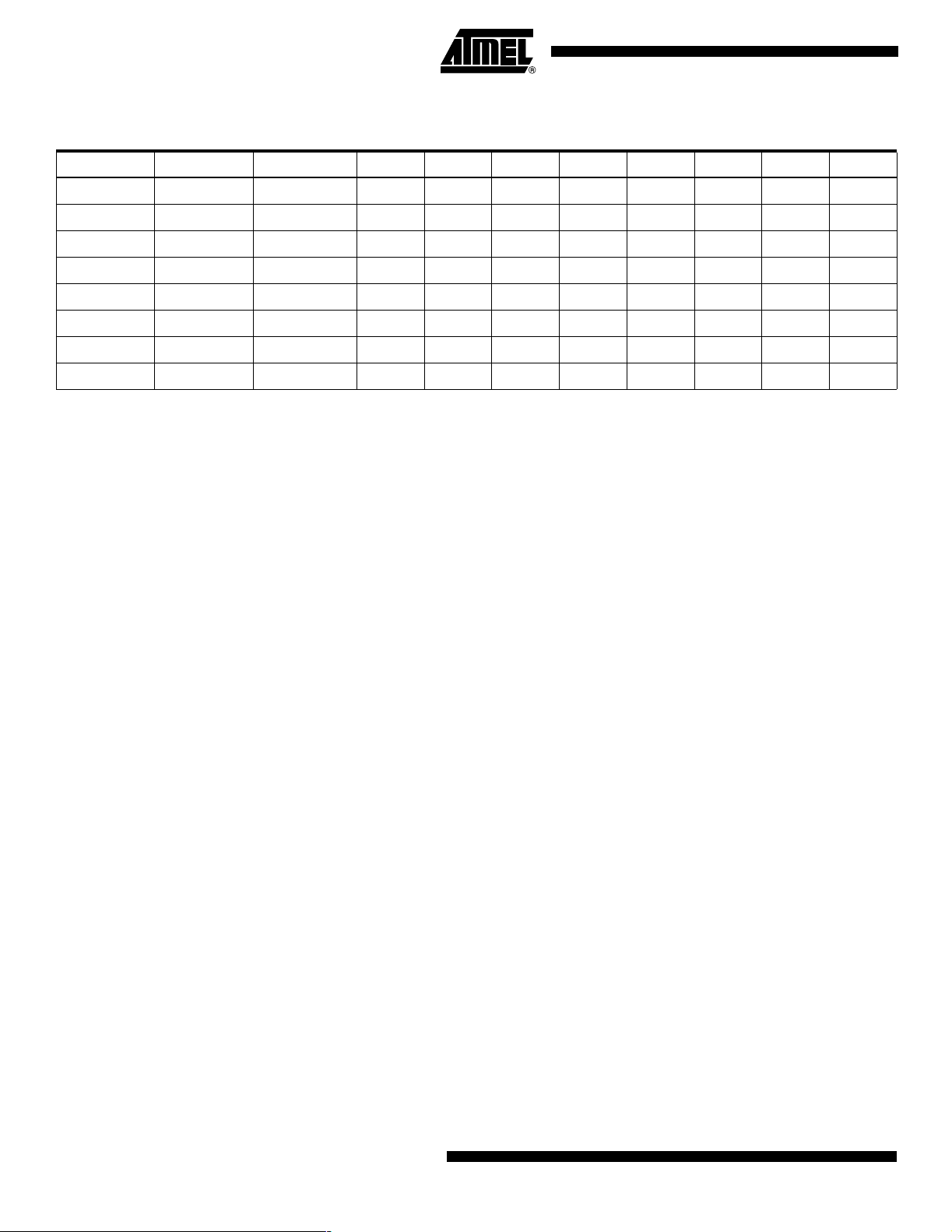
Pin Configurations
Pin Name Function
A0 - A16 Flash/SRAM Common Address Input for 2M SRAM
A0 - A17 Flash/SRAM Common Address Input for 4M SRAM
A18 - A19 Flash Address Input
CE
OE
/SOE Flash/SRAM, Output Enable
WE
/SWE Flash/SRAM, Write Enable
Flash Chip Enable
VCC Flash Power Supply
VPP Optional Flash Power Supply for Faster Program/Erase Operations
I/O0-I/O15 Data Inputs/Outputs
SCS1
, SCS2 SRAM Chip Select
RDY/BUSY
Flash Ready/Busy Output
SVCC SRAM Power Supply
GND/SGND Flash/SRAM GND
SUB
SLB
SRAM Upper Byte
SRAM Lower Byte
NC No Connect
RESET
Flash Reset
2
AT52BR1672(T)/1674(T)
2604B–STKD–09/02
AT52BR1672(T)/1674(T)
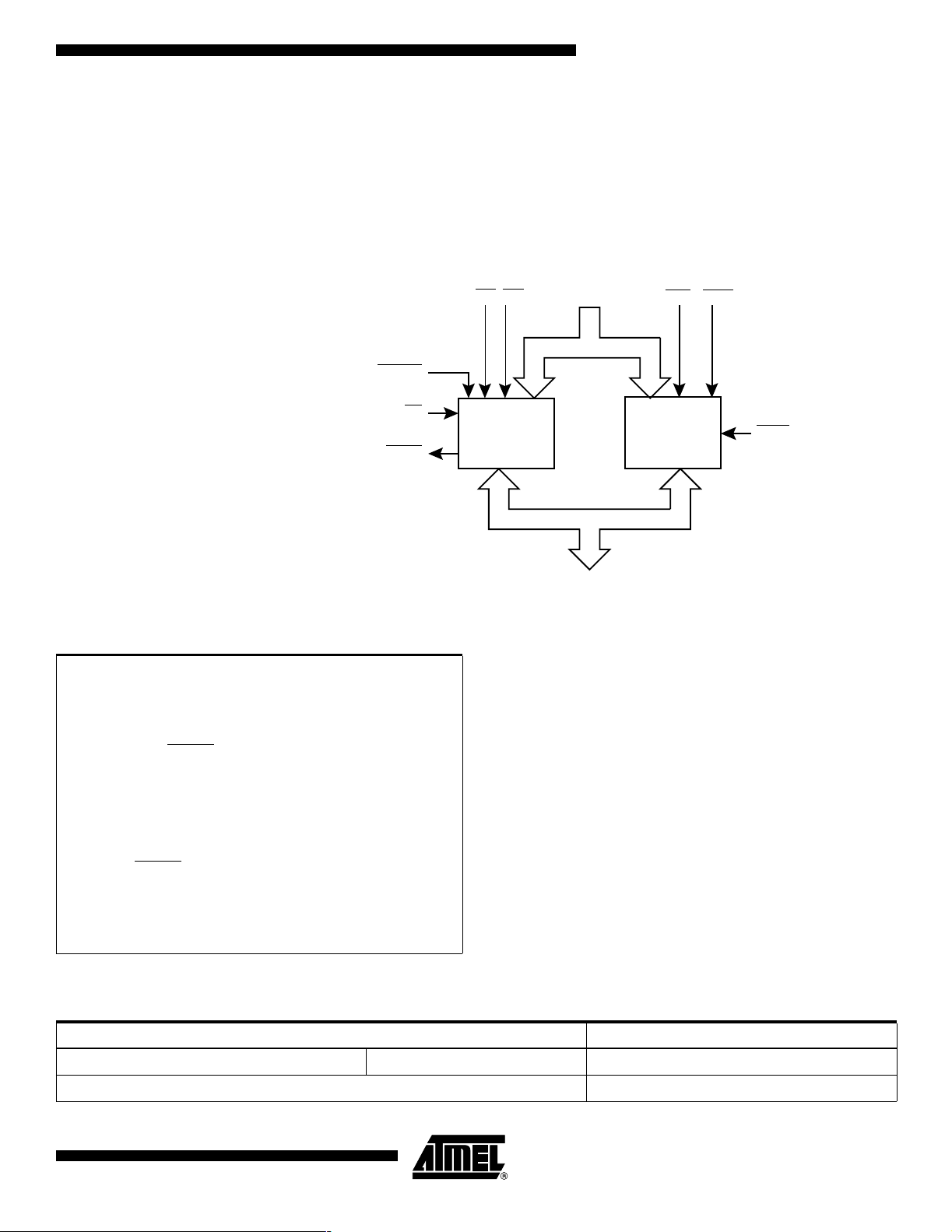
Description The AT52BR1672(T) combines a 16-megabit Flash (1M x 16) and a 2-megabit SRAM (orga-
nized as 128K x 16) in a stacked CBGA package; while the AT52BR1674(T) combines a 16megabit Flash (1M x 16) and a 4-megabit SRAM (organized as 256K x 16) in a stacked CBGA
package. Both devices operate at 2.7V to 3.3V in the industrial temperature range. The modules use a 16-megabit Flash with dual plane architecture for concurrent read/write operations.
The Flash is organized as 12M + 4M for planes B and A, respectively.
Block Diagram
WEOE SWESOE
RESET
CE
FLASH SRAM
RDY/BUSY
ADDRESS
SCS1
Absolute Maximum Ratings
Temperature under Bias .................................. -40°Cto+85°C
Storage Temperature ..................................... -55°Cto+150°C
All Input Voltages
except V
(including NC Pins)
with Respect to Ground .....................................-0.2V to +3.3V
Voltage on V
with Respect to Ground ..................................-0.2V to + 6.25V
Voltage on RESET
with Respect to Ground ...................................-0.2V to +13.5V
All Output Voltages
with Respect to Ground .....................................-0.2V to +0.2V
and RESET
PP
PP
DC and AC Operating Range
DATA
*NOTICE: Stresses beyond those listed under “Absolute
Maximum Ratings” may cause permanent damage to the device. This is a stress rating only and
functional operation of the device at these or any
other conditions beyond those indicated in the
operational sections of this specification is not
implied. Exposure to absolute maximum rating
conditions for extended periods may affect
device reliability.
AT52BR1672(T)/1674(T)
Operating Temperature (Case) Industrial -40°C-85°C
V
Power Supply 2.7V to 3.3V
CC
2604B–STKD–09/02
3

16-megabit Flash Description
The 16-megabit Flash memory organized as 1,048,576 words of 16 bits each. The x16 data
appears on I/O0 - I/O15. The memory is divided into 39 sectors for erase operations.The
device has CE
reprogrammed using a single 2.7V power supply, making it ideally suited for in-system
programming.
The device powers on in the read mode. Command sequences are used to place the device in
other operation modes such as program and erase. The device has the capability to protect
the data in any sector (see Sector Lockdown section).
The device is segmented into two memory planes. Reads from memory plane B may be performed even while program or erase functions are being executed in memory plane A and vice
versa. This operation allows improved system performance by not requiring the system to wait
for a program or erase operation to complete before a read is performed. To further increase
the flexibility of the device, it contains an Erase Suspend feature. This feature will put the
erase on hold for any amount of time and let the user read data from or program data to any of
the remaining sectors within the same memory plane. There is no reason to suspend the
erase operation if the data to be read is in the other memory plane. The end of a program or
an erase cycle is detected by the Ready/Busy
and OE control signals to avoid any bus contention. This device can be read or
pin, Data Polling or by the toggle bit.
The VPP pin provides faster program/erase times. With V
erase operations are accelerated.
A six-byte command (Enter Single Pulse Program Mode) sequence to remove the requirement
of entering the three-byte program sequence is offered to further improve programming time.
After entering the six-byte code, only single pulses on the write control lines are required for
writing into the device. This mode (Single Pulse Word Program) is exited by powering down
the device, or by pulsing the RESET
to V
. Erase and Erase Suspend/Resume commands will not work while in this mode; if
CC
entered they will result in data being programmed into the device. It is not recommended that
the six-byte code reside in the software of the final product but only exist in external programming code.
pin low for a minimum of 500 ns and then bringing it back
at 5.0V or 12.0V, the program and
PP
4
AT52BR1672(T)/1674(T)
2604B–STKD–09/02
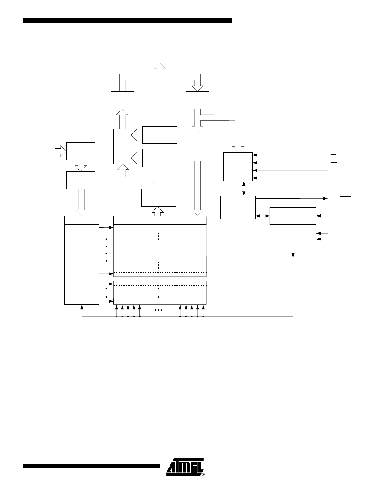
16-megabit Flash Memory Block Diagram
I/O0 - I/O15
AT52BR1672(T)/1674(T)
A0 - A19
INPUT
BUFFER
ADDRESS
LATCH
Y-DECODER
X-DECODER
OUTPUT
BUFFER
OUTPUT
IDENTIFIER
MULTIPLEXER
COMPARATOR
PLANE B
SECTORS
REGISTER
STATUS
REGISTER
DATA
Y-GATING
INPUT
BUFFER
DATA
REGISTER
COMMAND
REGISTER
WRITE STATE
MACHINE
PROGRAM/ERASE
VOLTAGE SWITCH
CE
WE
OE
RESET
RDY/BUSY
VPP
VCC
GND
2604B–STKD–09/02
PLANE A SECTORS
5

Device Operation
READ: The 16-megabit Flash is accessed like an EPROM. When CE and OE are low and WE
is high, the data stored at the memory location determined by the address pins are asserted
on the outputs. The outputs are put in the high-impedance state whenever CE
or OE is high.
This dual-line control gives designers flexibility in preventing bus contention.
COMMAND SEQUENCES: When the device is first powered on it will be reset to the read or
standby mode, depending upon the state of the control line inputs. In order to perform other
device functions, a series of command sequences are entered into the device. The command
sequences are shown in the Command Definitions table (I/O8 - I/O15 are don’t care inputs for
the command codes). The command sequences are written by applying a low pulse on the
WE
or CE input with CE or WE low (respectively) and OE high. The address is latched on the
falling edge of CE
CE
or WE. Standard microprocessor write timings are used. The address locations used in the
or WE, whichever occurs last. The data is latched by the first rising edge of
command sequences are not affected by entering the command sequences.
RESET: A RESET
a logic high level, the device is in its standard operating mode. A low level on the RESET
input pin is provided to ease some system applications. When RESET is at
input
halts the present device operation and puts the outputs of the device in a high-impedance
state. When a high level is reasserted on the RESET
pin, the device returns to the read or
standby mode, depending upon the state of the control inputs.
ERASURE: Before a word can be reprogrammed, it must be erased. The erased state of
memory bits is a logical “1”. The entire device can be erased by using the Chip Erase command or individual sectors can be erased by using the Sector Erase command.
CHIP ERASE: The entire device can be erased at one time by using the six-byte chip erase
software code. After the chip erase has been initiated, the device will internally time the erase
operation so that no external clocks are required. The maximum time to erase the chip is t
EC
If the sector lockdown has been enabled, the chip erase will not erase the data in the sector
that has been locked out; it will erase only the unprotected sectors. After the chip erase, the
device will return to the read or standby mode.
SECTOR ERASE: As an alternative to a full chip erase, the device is organized into 39 sectors (SA0 - SA38) that can be individually erased. The Sector Erase command is a six-bus
cycle operation. The sector address is latched on the falling WE
the 30H data input command is latched on the rising edge of WE
the rising edge of WE
of the sixth cycle. The erase operation is internally controlled; it will
automatically time to completion. The maximum time to erase a section is t
edge of the sixth cycle while
. The sector erase starts after
. When the sec-
SEC
tor programming lockdown feature is not enabled, the sector will erase (from the same Sector
Erase command). An attempt to erase a sector that has been protected will result in the operation terminating in 2 µs.
.
WORD PROGRAMMING: Once a memory block is erased, it is programmed (to a logical “0”)
on a word-by-word basis. Programming is accomplished via the internal device command register and is a four-bus cycle operation. The device will automatically generate the required
internal program pulses.
Any commands written to the chip during the embedded programming cycle will be ignored. If
a hardware reset happens during programming, the data at the location being programmed
will be corrupted. Please note that a data “0” cannot be programmed back to a “1”;onlyerase
operations can convert “0”sto“1”s. Programming is completed after the specified t
time. The Data
Polling feature or the Toggle Bit feature may be used to indicate the end of a
BP
cycle
program cycle.
VPP PIN: The circuitry of the 16-megabit Flash is designed so that the device can be programmed or erased from the V
than or equal to the VCC pin, the device selects the V
6
AT52BR1672(T)/1674(T)
power supply or from the VPP input pin. When VPPis less
CC
supply for programming and erase
CC
2604B–STKD–09/02

AT52BR1672(T)/1674(T)
operations. When the VPP pin is greater than the VCCsupply, the device will select the V
PP
input as the power supply for programming and erase operations. The device will allow for
some variations between the V
input and the VCCpower supply in its selection of VCCor V
PP
PP
for program or erase operations. If the VPP pin is within 0.3V of VCCfor 2.7V < VCC<3.3V,
then the program or erase operations will use V
the V
signal is used to accelerate program and erase operations, the VPPmust be in the 5V
PP
± 0.5V or 12V ± 0.5V range to ensure proper operation. The V
and disregard the VPPinput signal. When
CC
pin can be left unconnected.
pp
SECTOR LOCKDOWN: Each sector has a programming lockdown feature. This feature prevents programming of data in the designated sectors once the feature has been enabled.
These sectors can contain secure code that is used to bring up the system. Enabling the lockdown feature will allow the boot code to stay in the device while data in the rest of the device is
updated. This feature does not have to be activated; any sector’s usage as a write protected
region is optional to the user.
At power-up or reset all sectors are unlocked. To activate the lockdown for a specific sector,
the six-bus cycle Sector Lockdown command must be issued. Once a sector has been locked
down, the contents of the sector is read-only and cannot be erased or programmed.
SECTOR LOCKDOWN DETECTION: A software method is available to determine if programming of a sector is locked down. When the device is in the software product identification
mode (see Software Product Identification Entry and Exit sections) a read from address location 00002H within a sector will show if programming the sector is locked down. If the data on
I/O0 is low, the sector can be programmed; if the data on I/O0 is high, the program lockdown
feature has been enabled and the sector cannot be programmed. The software product identification exit code should be used to return to standard operation.
SECTOR LOCKDOWN OVERRIDE: The only way to unlock a sector that is locked down is
through reset or power-up cycles. After power-up or reset, the content of a sector that is
locked down can be erased and reprogrammed.
ERASE SUSPEND/ERASE RESUME: TheEraseSuspendcommandallowsthesystemto
interrupt a sector erase operation and then program or read data from a different sector within
the same plane. Since this device has a dual-plane architecture, there is no need to use the
Erase Suspend feature while erasing a sector when you want to read data from a sector in the
other plane. After the Erase Suspend command is given, the device requires a maximum time
of 15 µs to suspend the erase operation. After the erase operation has been suspended, the
plane that contains the suspended sector enters the erase-suspend-read mode. The system
can then read data or program data to any other sector within the device. An address is not
required during the Erase Suspend command. During a sector erase suspend, another sector
cannot be erased. To resume the sector erase operation, the system must write the Erase
Resume command. The Erase Resume command is a one-bus cycle command, which does
require the plane address (determined by A18 and A19). The device also supports an erase
suspend during a complete chip erase. While the chip erase is suspended, the user can read
from any sector within the memory that is protected. The command sequence for a chip erase
suspend and a sector erase suspend are the same.
PRODUCT IDENTIFICATION: The product identification mode identifies the device and manufacturer as Atmel. It may be accessed by hardware or software operation. The hardware
operation mode can be used by an external programmer to identify the correct programming
algorithm for the Atmel product.
For details, see “Operating Modes” on page 13 (for hardware operation) or “Software Product
Identification Entry/Exit” on page 21. The manufacturer and device codes are the same for
both modes.
2604B–STKD–09/02
7

128-BIT PROTECTION REGISTER: The 16-megabit Flash contains a 128-bit register that
can be used for security purposes in system design. The protection register is divided into two
64-bit blocks. The two blocks are designated as block A and block B. The data in block A is
non-changeable and is programmed at the factory with a unique number. The data in block B
is programmed by the user and can be locked out such that data in the block cannot be reprogrammed. To program block B in the protection register, the four-bus cycle Program
Protection Register command must be used as shown in the Command Definition table on
page 9. To lock out block B, the four-bus cycle Lock Protection Register command must be
used as shown in the Command Definition table. Data bit D1 must be zero during the fourth
bus cycle. All other data bits during the fourth bus cycle are don’t cares. Please see the “Protection Register Addressing Table” on page 10 for the address locations in the protection
register. To read the protection register, the Product ID Entry command is given followed by a
normal read operation from an address within the protection register. After reading the protection register, the Product ID Exit command must be given prior to performing any other
operation.
DATA
POLLING: The Flash features Data Polling to indicate the end of a program cycle. Dur-
ing a program cycle an attempted read of the last word loaded will result in the complement of
the loaded data on I/O7. Once the program cycle has been completed, true data is valid on all
outputs and the next cycle may begin. During a chip or sector erase operation, an attempt to
read the device will give a “0” on I/O7. Once the program or erase cycle has completed, true
data will be read from the device. Data
Polling may begin at any time during the program
cycle. Please see “Status Bit Table” on page 22 for more details.
TOGGLE BIT: In addition to Data
Polling, the 16-megabit Flash provides another method for
determining the end of a program or erase cycle. During a program or erase operation, successive attempts to read data from the same memory plane will result in I/O6 toggling between
one and zero. Once the program cycle has completed, I/O6 will stop toggling and valid data
will be read. Examining the toggle bit may begin at any time during a program cycle.
An additional toggle bit is available on I/O2, which can be used in conjunction with the toggle
bit that is available on I/O6. While a sector is erase suspended, a read or a program operation
from the suspended sector will result in the I/O2 bit toggling. Please see “Status Bit Table” on
page 22 for more details.
RDY/BUSY
another method of detecting the end of a program or erase operation. RDY/BUSY
: For the 16-megabit Flash, an open-drain Ready/Busy output pin provides
is actively
pulled low during the internal program and erase cycles and is released at the completion of
the cycle. The open-drain connection allows for OR-tying of several devices to the same
RDY/BUSY
line.
HARDWARE DATA PROTECTION: The Hardware Data Protection feature protects against
inadvertent programs to the Flash in the following ways: (a) V
(typical), the program function is inhibited. (b) V
V
sense level, the device will automatically time out 10 ms (typical) before programming. (c)
CC
Program inhibit: holding any one of OE
low, CE high or WE high inhibits program cycles. (d)
Noise filter: pulses of less than 15 ns (typical) on the WE
power-on delay: once VCChas reached the
CC
or CE inputs will not initiate a pro-
sense: if VCCis below 1.8V
CC
gram cycle.
INPUT LEVELS: While operating with a 2.7V to 3.3V power supply, the address inputs and
control inputs (OE
operation of the device. The I/O lines can only be driven from 0 to V
OUTPUT LEVELS: For the 16-megabit Flash, output high levels (V
0.2V (not V
levels, V
CC
CCQ
,CEand WE) may be driven from 0 to 5.5V without adversely affecting the
+0.6V.
CC
) are equal to V
). For 2.7V - 3.3V output levels, V
must be tied to VCC. For 1.8V - 2.2V output
CCQ
OH
CCQ
must be regulated to 2.0V ± 10%, while VCCmust be regulated to 2.7V - 3.0V (for
minimum power).
-
8
AT52BR1672(T)/1674(T)
2604B–STKD–09/02
AT52BR1672(T)/1674(T)
OUT
30
(1)
2nd Bus
Cycle
(2)
55 555 80 555 AA AAA 55 555 10
IN
3rd Bus
Cycle
4th Bus
Cycle
OUT
5th Bus
Cycle
IN
IN
(7)
6th Bus
Cycle
(3)(4)
(3)(4)
30
60
CommandDefinitioninHex
1st Bus
Command
Sequence
Read 1 Addr D
Chip Erase 6 555 AA AAA
Sector Erase 6 555 AA AAA 55 555 80 555 AA AAA 55 SA
Word Program 4 555 AA AAA 55 555 A0 Addr D
Enter Single Pulse
Program Mode
Single Pulse
Word Prog ram
Sector Lockdown 6 555 AA AAA 55 555 80 555 AA AAA 55 SA
Erase Suspend 1 XXX B0
Erase Resume 1 PA
Product ID Entry 3 555 AA AAA 55 555 90
Product ID Exit
Product ID Exit
Program Protection
Register
Lock Protection
Register - Block B
Status of Block B
Protection
(6)
(6)
Bus
Cycles
6 555 AA AAA 55 555 80 555 AA AAA 55 555 A0
1AddrD
3 555 AA AAA 55 555 F0
1 XXX F0
4 555 AA AAA 55 555 C0 Addr D
4 555 AA AAA 55 555 C0 080 X0
4 555 AA AAA 55 555 90 80 D
Cycle
Addr Data Addr Data Addr Data Addr Data Addr Data Addr Data
(5)
Notes: 1. The DATA FORMAT shown for each bus cycle is as follows; I/O7 - I/O0 (Hex). In word operation I/O15 - I/O8 are Don’tCare.
The ADDRESS FORMAT shown for each bus cycle is as follows: A11 - A0 (Hex). Address A19 through A11 are Don’tCare.
2. Since A11 is a Don’t Care, AAA can be replaced with 2AA.
3. SA = sector address. Any word address within a sector can be used to designate the sector address (see page 11 for
details).
4. Once a sector is in the lockdown mode, data in the protected sector cannot be changed unless the chip is reset or power
cycled.
5. PA is the plane address (A19-A18).
6. Either one of the Product ID Exit commands can be used.
7. If data bit D1 is “0”, block B is locked. If data bit D1 is “1”, block B can be reprogrammed.
Absolute Maximum Ratings*
Temperature under Bias ................................ -55°Cto+125°C
Storage Temperature ..................................... -65°Cto+150°C
All Input Voltages
(including NC Pins)
with Respect to Ground ...................................-0.6V to +6.25V
All Output Voltages
with Respect to Ground .............................-0.6V to V
Voltage on OE
and V
PP
with Respect to Ground ...................................-0.6V to +13.0V
2604B–STKD–09/02
CC
+0.6V
*NOTICE: Stresses beyond those listed under “Absolute
Maximum Ratings” may cause permanent damage to the device. This is a stress rating only and
functional operation of the device at these or any
other conditions beyond those indicated in the
operational sections of this specification is not
implied. Exposure to absolute maximum rating
conditions for extended periods may affect
device reliability.
9
Protection Register Addressing Table
Word Use Block A7 A6 A5 A4 A3 A2 A1 A0
0 Factory A 10000001
1 Factory A 10000010
2 Factory A 10000011
3 Factory A 10000100
4 User B 10000101
5 User B 10000110
6 User B 10000111
7 User B 10001000
Note: 1. All address lines not specified in the above table must be 0 when accessing the protection register, i.e., A19 - A8 = 0.
10
AT52BR1672(T)/1674(T)
2604B–STKD–09/02
AT52BR1672(T)/1674(T)
Top Boot 16-megabit Flash (12M + 4M) – Sector Address Table
Plane Sector Size (Words)
B SA0 32K 00000 - 07FFF
B SA1 32K 08000 - 0FFFF
B SA2 32K 10000 - 17FFF
B SA3 32K 18000 - 1FFFF
B SA4 32K 20000 - 27FFF
B SA5 32K 28000 - 2FFFF
B SA6 32K 30000 - 37FFF
B SA7 32K 38000 - 3FFFF
B SA8 32K 40000 - 47FFF
B SA9 32K 48000 - 4FFFF
B SA10 32K 50000 - 57FFF
B SA11 32K 58000 - 5FFFF
B SA12 32K 60000 - 67FFF
B SA13 32K 68000 - 6FFFF
B SA14 32K 70000 - 77FFF
B SA15 32K 78000 - 7FFFF
B SA16 32K 80000 - 87FFF
B SA17 32K 88000 - 8FFFF
B SA18 32K 90000 - 97FFF
B SA19 32K 98000 - 9FFFF
B SA20 32K A0000 - A7FFF
B SA21 32K A8000 - AFFFF
B SA22 32K B0000 - B7FFF
B SA23 32K B8000 - BFFFF
A SA24 32K C0000 - C7FFF
A SA25 32K C8000 - CFFFF
A SA26 32K D0000 - D7FFF
A SA27 32K D8000 - DFFFF
A SA28 32K E0000 - E7FFF
A SA29 32K E8000 - EFFFF
A SA30 32K F0000 - F7FFF
A SA31 4K F8000 - F8FFF
A SA32 4K F9000 - F9FFF
A SA33 4K FA000 - FAFFF
A SA34 4K FB000 - FBFFF
A SA35 4K FC000 - FCFFF
A SA36 4K FD000 - FDFFF
A SA37 4K FE000 - FEFFF
A SA38 4K FF000 - FFFFF
Address Range (A19 - A0)
x16
2604B–STKD–09/02
11
Bottom Boot 16-megabit Flash (12M + 4M) – Sector Address Table
x16
Plane Sector Size (Words)
A SA0 4K 00000 - 00FFF
A SA1 4K 01000 - 01FFF
A SA2 4K 02000 - 02FFF
A SA3 4K 03000 - 03FFF
A SA4 4K 04000 - 04FFF
A SA5 4K 05000 - 05FFF
A SA6 4K 06000 - 06FFF
A SA7 4K 07000 - 07FFF
A SA8 32K 08000 - 0FFFF
A SA9 32K 10000 - 17FFF
A SA10 32K 18000 - 1FFFF
A SA11 32K 20000 - 27FFF
A SA12 32K 28000 - 2FFFF
A SA13 32K 30000 - 37FFF
A SA14 32K 38000 - 3FFFF
B SA15 32K 40000 - 47FFF
B SA16 32K 48000 - 4FFFF
B SA17 32K 50000 - 57FFF
B SA18 32K 58000 - 5FFFF
B SA19 32K 60000 - 67FFF
B SA20 32K 68000 - 6FFFF
B SA21 32K 70000 - 77FFF
B SA22 32K 78000 - 7FFFF
B SA23 32K 80000 - 87FFF
B SA24 32K 88000 - 8FFFF
B SA25 32K 90000 - 97FFF
B SA26 32K 98000 - 9FFFF
B SA27 32K A0000 - A7FFF
B SA28 32K A8000 - AFFFF
B SA29 32K B0000 - B7FFF
B SA30 32K B8000 - F7FFF
B SA31 32K C0000 - C7FFF
B SA32 32K C8000 - CFFFF
B SA33 32K D0000 - D7FFF
B SA34 32K D8000 - DFFFF
B SA35 32K E0000 - E7FFF
B SA36 32K E8000 - EFFFF
B SA37 32K F0000 - F7FFF
B SA38 32K F8000 - FFFFF
Address Range (A19 - A0)
12
AT52BR1672(T)/1674(T)
2604B–STKD–09/02
 Loading...