

BDTIC www.BDTIC.com/ATMEL
Features
• Single-voltage Operation
–5V Read
– 5V Reprogramming
• Fast Read Access Time – 45 ns
• Internal Program Control and Timer
• 8K Word Boot Block with Lockout
• Fast Erase Cycle Time – 1.5 seconds
• Word-by-word Programming – 10 µs/Word Typical
• Hardware Data Protection
• Data Polling for End of Program Detection
• Small 10 x 14 mm VSOP Package
• Typical 10,000 Write Cycles
1-megabit
(64K x 16)
Description
The AT49F1024A is a 5-volt-only in-system Flash memory organized as 65,536 words
by 16 bits. Manufactured w ith Atmel ’s advance d nonvolatile CMO S techno logy, the
devices offer access times to 45 ns with power dissipation of just 275 mW over the
commercial temp erature range. Whe n the device is desele cted, the CMOS stand by
current is less than 100 µA.
To allow for simple in-system reprogrammability, the AT49F1024A does not require
high-input voltages for programming. Five-volt-only commands determine the read
and programming operation of the device. Reading da ta out of th e device is simila r to
reading from an EPROM. Reprogramming the A T49F1024A is performed by erasing a
block of data (entire chip or main memory block) and then programming on a word-byword basis. The typical word p rogramming t ime is a fast 10 µs. T he end of a program
cycle can be optionally detected by the Data
program cycle has been detected, a new access for a read or program can begin. The
typical number of program and erase cycles is in excess of 10,000 cycles.
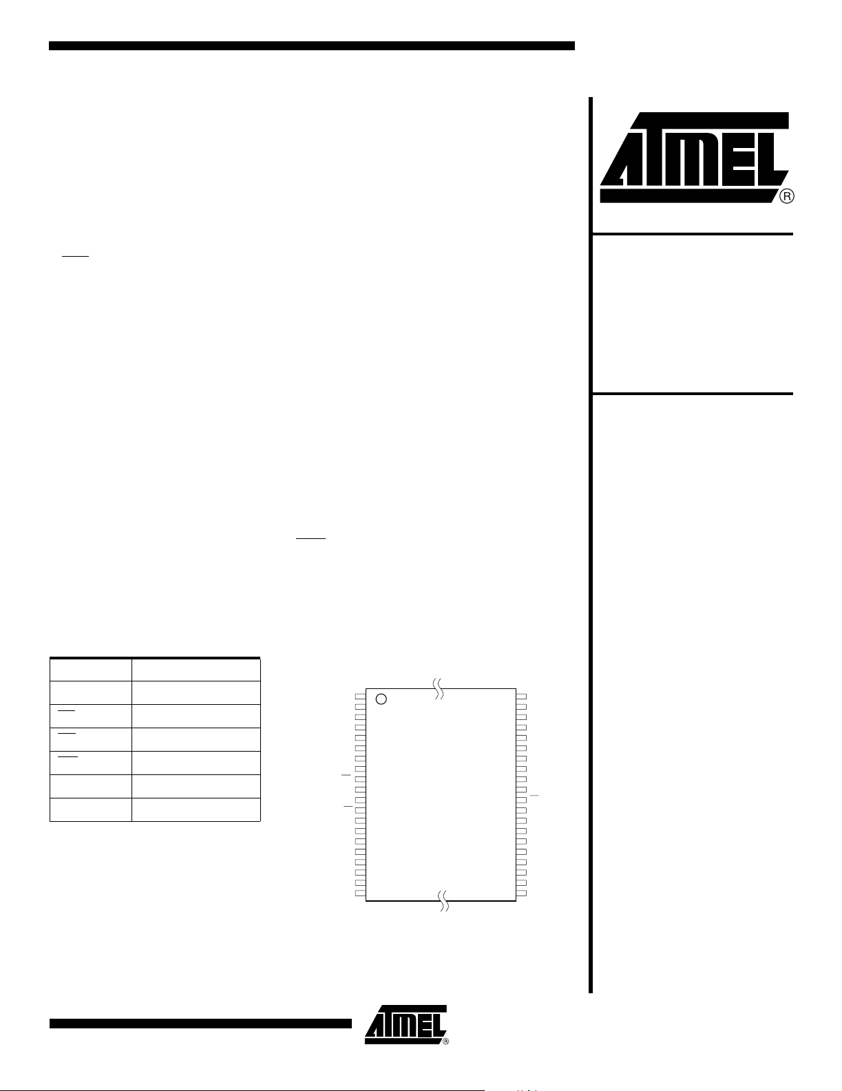
Pin Configurations
Pin Name Function
A0 - A15 Addresses
CE
OE Output Enable
WE
I/O0 - I/O15 Data Inputs/Outputs
NC No Connect
Chip Enable
Write Enable
Polling feature. Once the end of a byte
VSOP Top View
Type 1
10 x 14 mm
A10
A11
A12
A13
A14
A15
WE
VCC
I/O15
I/O14
I/O13
I/O12
I/O11
I/O10
I/O9
I/O8
1
A9
2
3
4
5
6
7
8
NC
9
10
11
NC
12
CE
13
14
15
16
17
18
19
20
40
GND
39
A8
38
A7
37
A6
36
A5
35
A4
34
A3
33
A2
32
A1
31
A0
30
OE
29
I/O0
28
I/O1
27
I/O2
26
I/O3
25
I/O4
24
I/O5
23
I/O6
22
I/O7
21
GND
5-volt Only
Flash Memory
AT49F1024A
3415B–FLASH–12/03
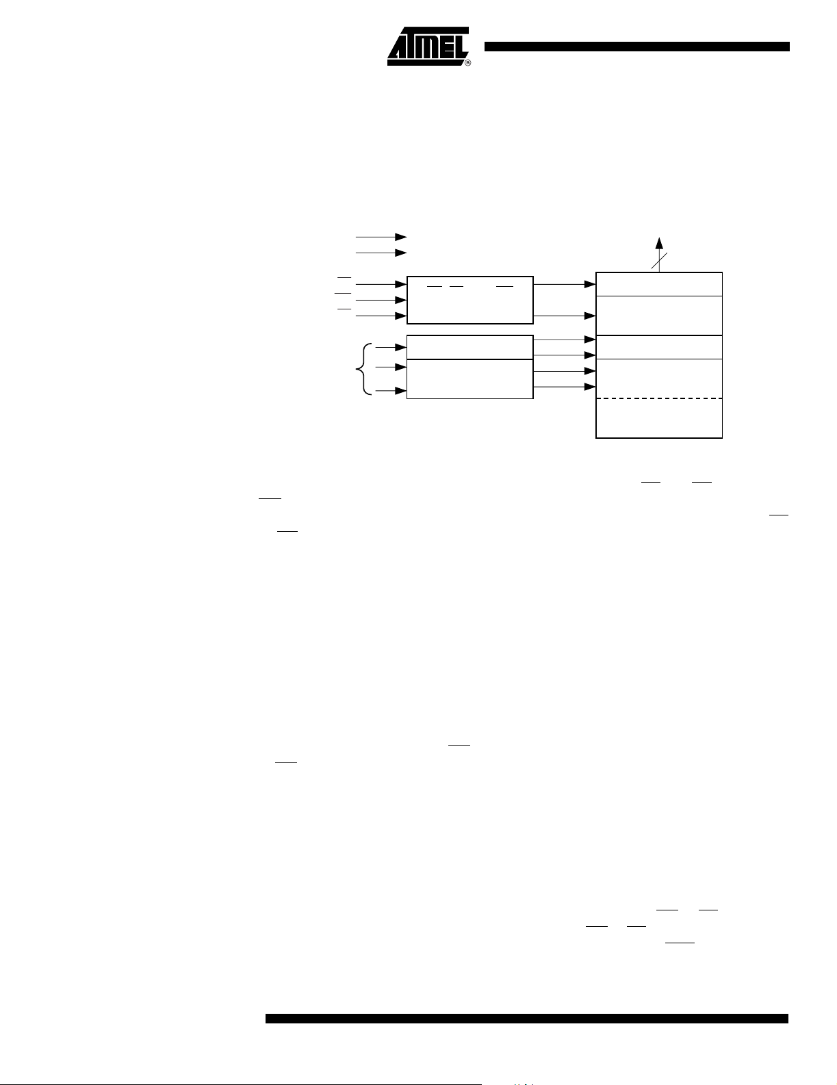
Block Diagram
The optional 8K word boot block section includes a reprogramming write lockout feature
to provide data integrity. The boot sector is designed to contain user secure code, and
when the feature is enabled, the boot sector is permanently protected from being erased
or reprogrammed.
DATA INPUTS/OUTPUTS
VCC
GND
I/O15 - I/O0
16
Device Operation
OE
WE
CE
ADDRESS
INPUTS
OE, CE, AND WE
LOGIC
Y DECODER
X DECODER
DATA LATCH
INPUT/OUTPUT
BUFFERS
Y-GATING
MAIN MEMORY
(56K WORDS)
OPTIONAL BOOT
BLOCK (8K WORDS)
FFFFH
2000H
1FFFH
0000H
READ: The AT49F1024A is accessed like an EPROM. When CE and OE are low and
is high, the data stored at the memory location determined by the address pins is
WE
asserted on the outputs. The ou tputs ar e put in the high impedan ce stat e whenev er CE
or OE is high. This dual line control giv es designers flexibility in preventing bus
contention.
CHIP ERASE: When the boot block programming lockout feature is not enabled, the
boot block and the m ain memor y block will eras e together fr om the s ame Chip Er ase
command (See Command Def initio ns tabl e). If the boot block lockout function has bee n
enabled, data in the boot s ec tio n wil l not be er as ed. Howev er, d ata i n the mai n m emo ry
section will be erased. After a chip erase, the device will return to the read mode.
MAIN MEMORY ERASE: As an alternative to the chip erase, a main memory block
erase can be performed, which will erase all words not located in the boot block region
to an FFFFH. Data located in the boot region will not be changed during a main memory
block erase. The Main Memory Erase command is a six-bus cycle operation . The
address (555H) is latche d on the fal li ng edg e o f the si xth c y cle wh il e th e 30 H da ta i np ut
is latched on the rising edge of WE
of the sixth cycle. Please see main mem ory erase cycl e waveforms. The main
of WE
. The main memory erase starts after the risi ng edg e
memory erase operation is internally controlled; it will automatically time to completion.
WORD PROGRAMMING: Once the memory array is erased, the device is programmed
(to a logic “0”) on a word-by-word basis. Please note that a data “0” cannot be
programmed back to a “1”; only erase operations can convert “0”s to “1”s. Programming
is accomplished via th e internal device command register a nd is a four-bus cycle
operation (please refer to the Comma nd Defi ni tion s tab le). T he dev ice wi ll automa tical ly
generate the required internal program pulses.
The program cycle has addresses latched on the falling edge of WE
occurs last, and the data latched on the rising edge of WE
Programming is completed after the specified t
cycle time. The Data Polling feature
BP
or CE, whichever occurs first.
or CE, whichever
may also be used to indicate the end of a program cycle.
2
AT49F1024A
3415B–FLASH–12/03

AT49F1024A
BOOT BLOCK PROGRAMMING LOCKOUT: The device has one designated block
that has a programming lockout feature. This feature prevents programming of data in
the designated bl ock once th e feature has been enabl ed. The siz e of the block is 8K
words. This block, referr ed to as the boot bloc k, can c onta in secur e co de tha t is use d to
bring up the system. Enab ling the l ockout featu re will allo w the boot cod e to stay in the
device while data in the rest of the device is updated. This feature does not have to be
activated; the boot block’s usage as a write-protected region is optional to the user. The
address range of the boot block is 0000H to 1FFFH.
Once the feature is en abled, the dat a in th e boot b lock c an no l onger be eras ed or pr ogrammed. Data in the ma in memory blo ck can still be ch anged through the regular
programming method an d c an be eras ed us in g e ith er th e Ch ip Er as e or th e M ai n M emory Block Eras e command. To activate the lockout featur e, a series of six pr ogram
commands to specific addresses with specific data must be performed. Please refer to
the Command Definitions table.
BOOT BLOCK LOCKOUT DETECTION: A software method is available to determine if
programming of the boo t block section is lock ed out. When the device is in the s oftware
product identification mode (see Software Produc t Identification Entry and Exit sections), a read from address location 0002H will show if programming the boot block is
locked out. If the data on I/O 0 is lo w, th e boot block can b e pro gramm ed; if the da ta on
I/O0 is high, the prog ram lockout fea ture has been activated and the bl ock can not be
programmed. The software product identification exit code should be used to return to
standard operation.
PRODUCT IDENTIFICATION: The product identification mode identifies the device and
manufacturer as Atmel. It may be accessed by hardware or software operation. The
hardware operation mode can be used by an external programmer to identify the correct
programming algorithm for the Atm el product.
For details, see Ope rating M odes ( for h ardware operatio n) or Software Prod uct Identi fication. The manufacturer and device code is the same for both modes.
POLLING: The AT49F1024A features Data Polling to indicate the end of a pro-
DAT A
gram or erase cycle. During a progra m cycle , an attem pted re ad of the l ast byte lo aded
will result in the compleme nt of the loaded data on I/O7. O nce the program cycle has
been completed, true data is valid on all outputs and the next cycle may begin. Data
Polling may begin at any time during the program cycle.
TOGGLE BIT: In addition to Data
determining the end of a prog ram or erase cycl e. During a prog ram or erase oper ation,
successive attempts to read data from the device will result in I/O6 toggling between
one and zero. Once the program cycle has completed, I/O6 will stop toggling and valid
data will be read. Exami ning the toggle bit may begin at any time during a program
cycle.
HARDWARE DATA PROTECTION: Hardware features protect against inadvertent programs to the AT49F1024A in the following ways: (a) V
(typical), the program function is inhibite d. (b) Program i nhibit: holdi ng any one of OE
low, CE high or WE high inhibits program cycles. (c) Noise filter: pulses of less than 15
ns (typical) on the WE
or CE inputs will not initiate a program cycle.
Polling, the AT49F1024A provides another method for
sense: if VCC is below 3.8V
CC
3415B–FLASH–12/03
3
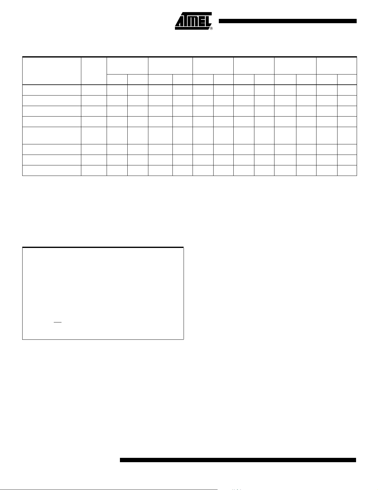
Command Definition (in Hex)
1st Bus
Command
Sequence
Bus
Cycles
Read 1 Addr D
Cycle
Addr Data Addr Data Addr Data Addr Data Addr Data Addr Data
OUT
Chip Erase 6 555 AA AAA
2nd Bus
Cycle
(2)
3rd Bus
Cycle
4th Bus
Cycle
5th Bus
Cycle
6th Bus
Cycle
55 555 80 555 AA AAA 55 555 10
Main Memory Erase 6 555 AA AAA 55 555 80 555 AA AAA 55 555 30
Word Program 4 555 AA AAA 55 555 A0 Addr D
Boot Block
Lockout
(3)
6 555 AA AAA 55 555 80 555 AA AAA 55 555 40
IN
Product ID Entry 3 555 AA AAA 55 555 90
Product ID Exit
Product ID Exit
(4)
(4)
3 555 AA AAA 55 555 F0
1xxxF0
Notes: 1. The DATA FORMAT in each bus cycle is as follows: I/O15 - I/O8 (Don’t Care); I/O7 - I/O0 (Hex).
The ADDRESS FORMAT in each bus cycle is as follows: A11 - A0 (Hex); A11 - A15 (Don’t Care).
2. Since A11 is a Don’t Care, AAA can be replaced with 2AA.
3. The 8K word boot sector has the address range 0000H to 1FFFH.
4. Either one of the Product ID Exit commands can be used.
Absolute Maximum Ratings*
Temperature under Bias ................................ -55°C to +125°C
Storage Temperature..................................... -65°C to +150°C
All Input Voltages
(including NC Pins)
with Respect to Ground...................................-0.6V to +6.25V
All Output Voltages
with Respect to Ground.............................-0.6V to V
+ 0.6V
CC
*NOTICE: Stresses beyond those listed under “Absolute
Maximum Ratings” may cause permanent damage to the dev ice . This i s a stress r at ing onl y and
functional operati on of the de vic e at these or an y
other conditions beyond those indicated in the
operational sections of this specification is not
implied. Exposure to absolute maximum rating
conditions for extended periods may affect
device reliability.
Voltage on OE
with Respect to Ground...................................-0.6V to +13.5V
4
AT49F1024A
3415B–FLASH–12/03

AT49F1024A
DC and AC Operating Range
AT49F1024A-45
Operating Temperature (Case) Com. 0°C - 70°C
V
Power Supply 5V ± 10%
CC
Operating Modes
Mode CE OE WE Ai I/O
Read V
(2)
Program
Standby/Write Inhibit V
IL
V
IL
IH
Program Inhibit X X V
Program Inhibit X V
Output Disable X V
Product Identification
Hardware V
Software
(5)
IL
Notes: 1. X can be VIL or VIH.
2. Refer to AC programming waveforms.
= 12.0V ± 0.5V.
3. V
H
4. Manufacturer Code: 001FH, Device Code: 0087H.
5. See details under “Software Product Identification Entry/Exit” on page 11.
V
IL
V
IH
(1)
X
IL
IH
V
IL
V
IH
V
IL
Ai D
Ai D
X X High-Z
IH
X
X High-Z
V
IH
A1 - A15 = VIL, A9 = V
A0 = VIL, A1 - A15 = V
A0 = VIH, A1 - A15 = V
A1 - A15 = VIL, A9 = V
(3)
H
(3)
, A0 = V
H
, A0 = V
IL
IL
IL
IH
OUT
IN
Manufacturer Code
Device Code
(4)
Manufacturer Code
Device Code
(4)
(4)
(4)
DC Characteristics
Symbol Parameter Condition Min Max Units
I
I
I
I
I
V
V
V
V
V
LI
LO
SB1
SB2
CC
(1)
IL
IH
OL
OH1
OH2
Input Load Current VIN = 0V to V
Output Leakage Current V
VCC Standby Current CMOS CE = VCC - 0.3V to V
VCC Standby Current TTL CE = 2.0V to V
V
Active Current f = 5 MHz; I
CC
Input Low Voltage 0.8 V
Input High Voltage 2.0 V
Output Low Voltage IOL = 2.1 mA 0.45 V
Output High Voltage IOH = -400 µA 2.4 V
Output High Voltage CMOS IOH = -100 µA; VCC = 4.5V 4.2 V
Note: 1. In the erase mode, I
3415B–FLASH–12/03
is 90 mA.
CC
= 0V to V
I/O
CC
CC
CC
CC
= 0 mA 50.0 mA
OUT
10.0 µA
10.0 µA
100.0 µA
1.0 mA
5

AC Read Characteristics
Symbol Parameter
t
t
t
t
t
ACC
CE
OE
DF
OH
(1)
(2)
(3)(4)
Address to Output Delay 45 ns
CE to Output Delay 45 ns
OE to Output Delay 0 30 ns
CE or OE to Output Float 0 25 ns
Output Hold from OE, CE or Address, whichever
occurred first
AT49F1024A-45
UnitsMin Max
0ns
AC Read Waveforms
(1)(2)(3)(4)
Notes: 1. CE may be delayed up to t
may be delayed up to tCE - tOE after the falling edge of CE without impact on tCE or by t
2. OE
without impact on t
is specified from OE or CE, whichever occurs first (CL = 5 pF).
3. t
DF
ACC
.
4. This parameter is characterized and is not 100% tested.
- tCE after the address transition without impact on t
ACC
ACC
.
- tOE after an address change
ACC
6
AT49F1024A
3415B–FLASH–12/03

Input Test W aveforms and Measurement Level
tR, tF < 5 ns
Output T est Load
5.0V
1.8K
OUTPUT
PIN
1.3K
30 pF
AT49F1024A
Pin Capacitance
f = 1 MHz, T = 25°C
Symbol Typ Max Units Conditions
C
IN
C
OUT
Note: 1. This parameter is characterized and is not 100% tested.
(1)
46pFV
812pFV
IN
OUT
= 0V
= 0V
3415B–FLASH–12/03
7

AC Word Load Characteristics
Symbol Parameter Min Max Units
tAS, t
t
AH
t
CS
t
CH
t
WP
t
DS
tDH, t
t
WPH
OES
OEH
Address, OE Setup Time 0 ns
Address Hold Time 50 ns
Chip Select Setup Time 0 ns
Chip Select Hold Time 0 ns
Write Pulse Width (WE or CE)50ns
Data Setup Time 50 ns
Data, OE Hold Time 0 ns
Write Pulse Width High 40 ns
AC Word Load Waveforms
WE Controlled
CE
Controlled
ADDRESS
WE
DATA IN
OE
ADDRESS
WE
OE
CE
t
OES
t
t
t
OES
t
AS
CS
AS
t
OEH
t
AH
t
WP
t
DS
t
AH
t
CH
t
OEH
t
CH
t
WPH
t
DH
t
CS
CE
t
WPH
t
WP
t
DS
t
DH
DATA IN
8
AT49F1024A
3415B–FLASH–12/03

AT49F1024A
Program Cycle Characteristics
Symbol Parameter Min Typ Max Units
t
BP
t
AS
t
AH
t
DS
t
DH
t
WP
t
WPH
t
EC
Program Cyc le Wa veforms
Word Programming Time 10 50 µs
Address Setup Time 0 ns
Address Hold Time 50 ns
Data Setup Time 50 ns
Data Hold Time 0 ns
Write Pulse Width 50 ns
Write Pulse Width High 40 ns
Erase Cycle Time 1.5 3 seconds
A0-A15
Main Memory or Chip Erase Cycle Waveforms
OE
CE
t
WP
WE
A0-A15
DATA
t
AS
t
AH
555
WORD 0
t
DH
AAA AAA
t
DS
AA
55 55
WORD 1 WORD 2
Notes: 1. OE must be high only when WE and CE are both low.
2. For chip erase, the address should be 10H. For a main memory erase, the data should be 30H.
t
555
WPH
555
80
AA
WORD 3
WORD 4
555
WORD 5
NOTE 2
t
EC
3415B–FLASH–12/03
9

Data Poll ing Char acteristics
(1)
Symbol Parameter Min Typ Max Units
t
DH
t
OEH
t
OE
t
WR
Data Hold Time 10 ns
OE Hold Time 10 ns
OE to Output Delay
(2)
Write Recovery Time 0 ns
Notes: 1. These parameters are characterized and not 100% tested.
2. See t
spec in “AC Read Characteristics” on page 6.
OE
Data Polling Waveforms
ns
Toggle Bit Characteristics
(1)
Symbol Parameter Min Typ Max Units
t
DH
t
OEH
t
OE
t
OEHP
t
WR
Data Hold Time 10 ns
OE Hold Time 10 ns
OE to Output Delay
(2)
OE High Pulse 150 ns
Write Recovery Time 0 ns
Notes: 1. These parameters are characterized and not 100% tested.
2. See t
Toggle Bit Waveforms
Notes: 1. Toggling either OE or CE or both OE and CE will operate toggle bit. The t
spec in “AC Read Characteristics” on page 6.
OE
(1)(2)(3)
specification must be met by the toggling
OEHP
input(s).
2. Beginning and ending state of I/O6 will vary.
3. Any address location may be used but the address should not vary.
ns
10
AT49F1024A
3415B–FLASH–12/03

AT49F1024A
Software Product Identification
Entry
(1)
LOAD DATA AA
TO
ADDRESS 555
LOAD DATA 55
TO
ADDRESS AAA
LOAD DATA 90
TO
ADDRESS 555
ENTER PRODUCT
IDENTIFICATION
(2)(3)(5)
MODE
Software Product Identification Exit
LOAD DATA AA
TO
ADDRESS 555
OR
LOAD DATA F0
TO
ANY ADDRESS
Boot Block Lockout Enable Algorithm
LOAD DATA AA
TO
ADDRESS 555
LOAD DATA 55
TO
ADDRESS AAA
LOAD DATA 80
TO
ADDRESS 555
LOAD DATA AA
TO
ADDRESS 555
LOAD DATA 55
TO
ADDRESS AAA
(1)
LOAD DATA 40
TO
ADDRESS 555
(1)
LOAD DATA 55
TO
ADDRESS AAA
LOAD DATA F0
TO
ADDRESS 555
EXIT PRODUCT
IDENTIFICATION
MODE
(4)
EXIT PRODUCT
IDENTIFICATION
MODE
(4)
Notes: 1. Data Format: I/O15 - I/O8 (Don’t Care); I/O7 - I/O0 (Hex).
Address Format: A11 - A0 (Hex); A11 - A15 (Don’t Care).
2. A1 - A15 = V
Manufacturer Code is read for A0 = V
.
IL
.
IL
Device Code is read for A0 = VIH.
3. The device does not remain in identification mode if
powered down.
4. The device returns to standard operation mode.
5. Manufacturer Code: 001FH
Device Code: 0087H
PAUSE 1 second
(2)
Notes: 1. Data Format: I/O15 - I/O8 (Don’t Care); I/O7 - I/O0 (Hex).
Address Format: A11 - A0 (Hex); A11 - A15 (Don’t Care).
2. Boot Block Lockout feature enabled.
3415B–FLASH–12/03
11

AT49F1024A Ordering Information
I
(mA)
t
ACC
(ns)
45 50 0.1 AT49F1024A-45VC 40V Commercial
45 50 0.1 AT49F1024A-45VL
CC
Ordering Code Package Operation RangeActive Standby
Lead Free
(0° to 70° C)
40V Commercial
(0° to 70° C)
Package Type
40V 40-lead, 10 mm x 14 mm, Thin Small Outline Package (VSOP)
12
AT49F1024A
3415B–FLASH–12/03

Packaging Information
40V – VSOP
AT49F1024A
PIN 1
Pin 1 Identifier
D1
D
e
E
b
A2
A
SEATING PLANE
A1
Notes: 1. This package conforms to JEDEC reference MO-142, Variation CA.
2. Dimensions D1 and E do not include mold protrusion. Allowable
protrusion on E is 0.15 mm per side and on D1 is 0.25 mm per side.
3. Lead coplanarity is 0.10 mm maximum.
0º ~ 8º
L
COMMON DIMENSIONS
SYMBOL
A – – 1.20
A1 0.05 – 0.15
A2 0.95 1.00 1.05
D 13.80 14.00 14.20
D1 12.30 12.40 12.50 Note 2
E 9.90 10.00 10.10 Note 2
L 0.50 0.60 0.70
L1 0.25 BASIC
b 0.17 0.22 0.27
c 0.10 – 0.21
e 0.50 BASIC
c
L1
GAGE PLANE
(Unit of Measure = mm)
MIN
NOM
MAX
NOTE
2325 Orchard Parkway
R
San Jose, CA 95131
3415B–FLASH–12/03
TITLE
40V, 40-lead (10 x 14 mm Package) Plastic Thin Small Outline
Package, Type I (VSOP)
DRAWING NO.
40V
10/18/01
REV.
B
13
 Loading...