

BDTIC www.BDTIC.com/ATMEL
Features
•
Single Voltage Operation Read/Write: 2.65V - 3.6V
•
Access Time – 70 ns
•
Sector Erase Architecture
– One Hundred Twenty-seven 32K Word (64K Bytes) Main Sectors with
Individual Write Lockout
– Eight 4K Word (8K Bytes) Sectors with Individual Write Lockout
•
Fast Word Program Time – 10 µs
•
Typical Sector Erase Time: 32K Word Sectors – 700 ms; 4K Word Sectors – 100 ms
•
Suspend/Resume Feature for Erase and Program
– Supports Reading and Programming Data from Any Sector by Suspending
Erase of a Different Sector
– Supports Reading Any Word by Suspending Programming of Any Other Word
•
Low-power Operation
– 10 mA Active
– 15 µA Standby
•
VPP Pin for Write Protection and Accelerated Program Operation
•
RESET Input for Device Initialization
•
Softlock Sector Protection
•
Secure Lock and Freeze Feature
•
Top or Bottom Boot Block Configuration Available
•
128-bit Protection Register
•
Minimum 100,000 Erase Cycles
•
Common Flash Interface (CFI)
•
CBGA Green (Pb/Halide-free/RoHS Compliant) Packaging
64-megabit
(4M x 16)
Secure
3-volt Only
Memory
AT49BV640S
AT49BV640ST
Summary
1. Description
The AT49BV640S(T) is a 2.7-volt 32-megabit Flash memory organized as 4,194,304
words of 16 bits each. The memory is divided into 135 sectors for erase operations.
The device is offered in a 64-ball CBGA package. The device has CE
signals to avoid any bus contention. This device can be read or reprogrammed using
a single power supply, making it ideally suited for in-system programming.
In some applications, in addition to the standard softlock sector protection mechanism, a requirement exists to allow for the permanent and irreversible locking of
selected regions in the memory. The AT49BV640S(T) allows the user to permanently
lock thirty-eight regions, and once activated these secure regions cannot be altered or
erased through Software or Hardware at any time. Once activated, no facility exists to
over-ride the secure lock mechanism. The size and the location of the secure regions
is determined by the Top or Bottom Boot Block designation. The location of the secure
regions is shown on pages 3 - 6.
The secure regions can be locked in any sequence and at any time during normal
device operation. Read operations can still be performed on any region that has the
secure lock feature enabled. Full read/write operations and standard sector operations including standard Sector locking can be performed on all regions that are not
secure locked.
and OE control
(Complete
Datasheet
under NDA)
NOTE: This is a summary document.
The complete document is available
under NDA. For more information,
please contact your local Atmel sales
office.
3583AS–FLASH–9/06
The AT49BV640S(T) device also contains a freeze feature that will freeze the lock status of the
secure regions. The freeze feature prevents any further locking of the secure regions. If the user
requires certain regions to be locked, then these regions must be programmed and locked prior
to activation of the freeze command. It is important to note that enabling the freeze feature is
irreversible.
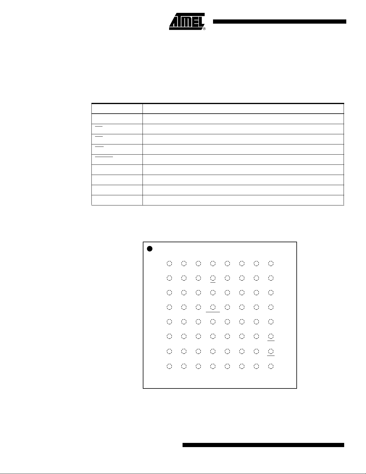
2. Pin Configurations
Pin Name Pin Function
A0 - A21 Addresses
CE Chip Enable
OE
Output Enable
WE
RESET
VPP Write Protection and Power Supply for Accelerated Program Operations
I/O0 - I/O15 Data Inputs/Outputs
NC No Connect
VCCQ Output Power Supply
2.1 64-ball CBGA Top View
Write Enable
Reset
A
B
C
D
E
F
G
H
2345678
1
A0
A1
A2
A3
I/O8
NC
NC
NC
A5
VSS
A6
A4
I/O1
I/O0
NC
NC
A7
A8
A9
A10
I/O9
I/010
I/O2
VCC
VPP
CE
A11
RESET
I/O3
I/O11
VCCQ
VSS
A12
A13
A14
NC
I/O4
I/O12
I/O5
I/O13
VCC
NC
NC
NC
NC
NC
I/O6
VSS
A17
A18
A19
A15
I/O15
NC
I/O14
I/O7
A21
NC
A20
A16
NC
OE
WE
NC
2
AT49BV640S(T) Summary
3583AS–FLASH–9/06
AT49BV640S(T) Summary
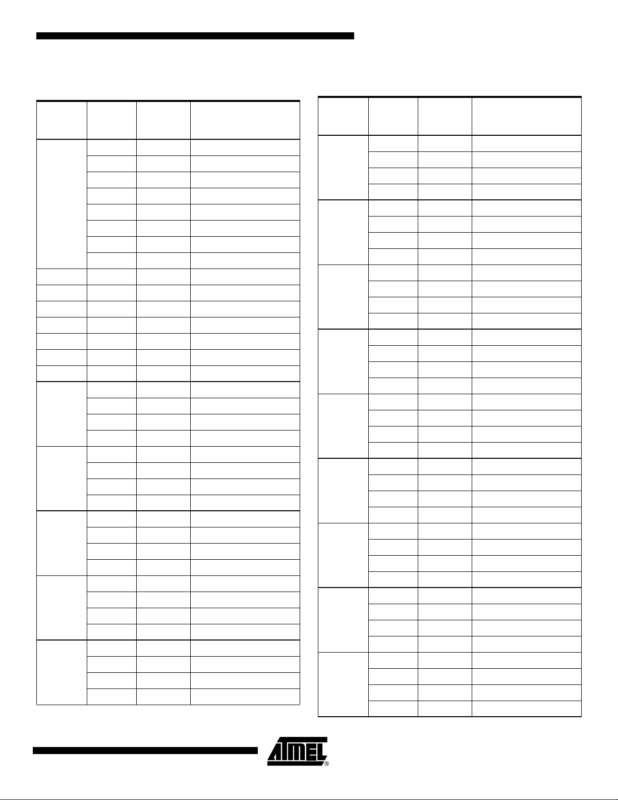
3. Memory Organization –
AT49BV640S
Secure
Region
(SCR) Sector
SA0 4K 00000 - 00FFF
SA1 4K 01000 - 01FFF
SA2 4K 02000 - 02FFF
0
1 SA8 32K 08000 - 0FFFF
2 SA9 32K 10000 - 17FFF
3 SA10 32K 18000 - 1FFFF
4 SA11 32K 20000 - 27FFF
5 SA12 32K 28000 - 2FFFF
6 SA13 32K 30000 - 37FFF
7 SA14 32K 38000 - 3FFFF
8
9
10
11
12
SA3 4K 03000 - 03FFF
SA4 4K 04000 - 04FFF
SA5 4K 05000 - 05FFF
SA6 4K 06000 - 06FFF
SA7 4K 07000 - 07FFF
SA15 32K 40000 - 47FFF
SA16 32K 48000 - 4FFFF
SA17 32K 50000 - 57FFF
SA18 32K 58000 - 5FFFF
SA19 32K 60000 - 67FFF
SA20 32K 68000 - 6FFFF
SA21 32K 70000 - 77FFF
SA22 32K 78000 - 7FFFF
SA23 32K 80000 - 87FFF
SA24 32K 88000 - 8FFFF
SA25 32K 90000 - 97FFF
SA26 32K 98000 - 9FFFF
SA27 32K A0000 - A7FFF
SA28 32K A8000 - AFFFF
SA29 32K B0000 - B7FFF
SA30 32K B8000 - BFFFF
SA31 32K C0000 - C7FFF
SA32 32K C8000 - CFFFF
SA33 32K D0000 - D7FFF
SA34 32K D8000 - DFFFF
Size
(Words)
Address Range
x16
(A21 - A0)
3. Memory Organization –
AT49BV640S (Continued)
Secure
Region
(SCR) Sector
SA35 32K E0000 - E7FFF
13
14
15
16
17
18
19
20
21
SA36 32K E8000 - EFFFF
SA37 32K F0000 - F7FFF
SA38 32K F8000 - FFFFF
SA39 32K 100000 - 107FFF
SA40 32K 108000 - 10FFFF
SA41 32K 110000 - 117FFF
SA42 32K 118000 - 11FFFF
SA43 32K 120000 - 127FFF
SA44 32K 128000 - 12FFFF
SA45 32K 130000 - 137FFF
SA46 32K 138000 - 13FFFF
SA47 32K 140000 - 147FFF
SA48 32K 148000 - 14FFFF
SA49 32K 150000 - 157FFF
SA50 32K 158000 - 15FFFF
SA51 32K 160000 - 167FFF
SA52 32K 168000 - 16FFFF
SA53 32K 170000 - 177FFF
SA54 32K 178000 - 17FFFF
SA55 32K 180000 - 187FFF
SA56 32K 188000 - 18FFFF
SA57 32K 190000 - 197FFF
SA58 32K 198000 - 19FFFF
SA59 32K 1A0000 - 1A7FFF
SA60 32K 1A8000 - 1AFFFF
SA61 32K 1B0000 - 1B7FFF
SA62 32K 1B8000 - 1BFFFF
SA63 32K 1C0000 - 1C7FFF
SA64 32K 1C8000 - 1CFFFF
SA65 32K 1D0000 - 1D7FFF
SA66 32K 1D8000 - 1DFFFF
SA67 32K 1E0000 - 1E7FFF
SA68 32K 1E8000 - 1EFFFF
SA69 32K 1F0000 - 1F7FFF
SA70 32K 1F8000 - 1FFFFF
Size
(Words)
x16
Address Range
(A21 - A0)
3583AS–FLASH–9/06
3

3. Memory Organization –
3. Memory Organization –
AT49BV640S (Continued)
Secure
Region
(SCR) Sector
SA71 32K 200000 - 207FFF
22
23
24
25
26
27
28
29
SA72 32K 208000 - 20FFFF
SA73 32K 210000 - 217FFF
SA74 32K 218000 - 21FFFF
SA75 32K 220000 - 227FFF
SA76 32K 228000 - 22FFFF
SA77 32K 230000 - 237FFF
SA78 32K 238000 - 23FFFF
SA79 32K 240000 - 247FFF
SA80 32K 248000 - 24FFFF
SA81 32K 250000 - 257FFF
SA82 32K 258000 - 25FFFF
SA83 32K 260000 - 267FFF
SA84 32K 268000 - 26FFFF
SA85 32K 270000 - 277FFF
SA86 32K 278000 - 27FFFF
SA87 32K 280000 - 287FFF
SA88 32K 288000 - 28FFFF
SA89 32K 290000 - 297FFF
SA90 32K 298000 - 29FFFF
SA91 32K 2A0000 - 2A7FFF
SA92 32K 2A8000 - 2AFFFF
SA93 32K 2B0000 - 2B7FFF
SA94 32K 2B8000 - 2BFFFF
SA95 32K 2C0000 - 2C7FFF
SA96 32K 2C8000 - 2CFFFF
SA97 32K 2D0000 - 2D7FFF
SA98 32K 2D8000 - 2DFFFF
SA99 32K 2E0000 - 2E7FFF
SA100 32K 2E8000 - 2EFFFF
SA101 32K 2F0000 - 2F7FFF
SA102 32K 2F8000 - 2FFFFF
Size
(Words)
x16
Address Range
(A21 - A0)
AT49BV640S (Continued)
Secure
Region
(SCR) Sector
SA103 32K 300000 - 307FFF
30
31
32
33
34
35
36
37
SA104 32K 308000 - 30FFFF
SA105 32K 310000 - 317FFF
SA106 32K 318000 - 31FFFF
SA107 32K 320000 - 327FFF
SA108 32K 328000 - 32FFFF
SA109 32K 330000 - 337FFF
SA110 32K 338000 - 33FFFF
SA111 32K 340000 - 347FFF
SA112 32K 348000 - 34FFFF
SA113 32K 350000 - 357FFF
SA114 32K 358000 - 35FFFF
SA115 32K 360000 - 367FFF
SA116 32K 368000 - 36FFFF
SA117 32K 370000 - 377FFF
SA118 32K 378000 - 37FFFF
SA119 32K 380000 - 387FFF
SA120 32K 388000 - 38FFFF
SA121 32K 390000 - 397FFF
SA122 32K 398000 - 39FFFF
SA123 32K 3A0000 - 3A7FFF
SA124 32K 3A8000 - 3AFFFF
SA125 32K 3B0000 - 3B7FFF
SA126 32K 3B8000 - 3BFFFF
SA127 32K 3C0000 - 3C7FFF
SA128 32K 3C8000 - 3CFFFF
SA129 32K 3D0000 - 3D7FFF
SA130 32K 3D8000 - 3DFFFF
SA131 32K 3E0000 - 3E7FFF
SA132 32K 3E8000 - 3EFFFF
SA133 32K 3F0000 - 3F7FFF
SA134 32K 3F8000 - 3FFFFF
Size
(Words)
x16
Address Range
(A21 - A0)
4
AT49BV640S(T) Summary
3583AS–FLASH–9/06

AT49BV640S(T) Summary
4. Memory Organization –
AT49BV640ST
Secure
Region
(SCR) Sector
SA0 32K 00000 - 07FFF
37
36
35
34
33
32
31
30
29
SA1 32K 08000 - 0FFFF
SA2 32K 10000 - 17FFF
SA3 32K 18000 - 1FFFF
SA4 32K 20000 - 27FFF
SA5 32K 28000 - 2FFFF
SA6 32K 30000 - 37FFF
SA7 32K 38000 - 3FFFF
SA8 32K 40000 - 47FFF
SA9 32K 48000 - 4FFFF
SA10 32K 50000 - 57FFF
SA11 32K 58000 - 5FFFF
SA12 32K 60000 - 67FFF
SA13 32K 68000 - 6FFFF
SA14 32K 70000 - 77FFF
SA15 32K 78000 - 7FFFF
SA16 32K 80000 - 87FFF
SA17 32K 88000 - 8FFFF
SA18 32K 90000 - 97FFF
SA19 32K 98000 - 9FFFF
SA20 32K A0000 - A7FFF
SA21 32K A8000 - AFFFF
SA22 32K B0000 - B7FFF
SA23 32K B8000 - BFFFF
SA24 32K C0000 - C7FFF
SA25 32K C8000 - CFFFF
SA26 32K D0000 - D7FFF
SA27 32K D8000 - DFFFF
SA28 32K E0000 - E7FFF
SA29 32K E8000 - EFFFF
SA30 32K F0000 - F7FFF
SA31 32K F8000 - FFFFF
SA32 32K 100000 - 107FFF
SA33 32K 108000 - 10FFFF
SA34 32K 110000 - 117FFF
SA35 32K 118000 - 11FFFF
Size
(Words)
x16
Address Range
(A21 - A0)
4. Memory Organization –
AT49BV640ST (Continued)
Secure
Region
(SCR) Sector
SA36 32K 120000 - 127FFF
28
27
26
25
24
23
22
21
20
SA37 32K 128000 - 12FFFF
SA38 32K 130000 - 137FFF
SA39 32K 138000 - 13FFFF
SA40 32K 140000 - 147FFF
SA41 32K 148000 - 14FFFF
SA42 32K 150000 - 157FFF
SA43 32K 158000 - 15FFFF
SA44 32K 160000 - 167FFF
SA45 32K 168000 - 16FFFF
SA46 32K 170000 - 177FFF
SA47 32K 178000 - 17FFFF
SA48 32K 180000 - 187FFF
SA49 32K 188000 - 18FFFF
SA50 32K 190000 - 197FFF
SA51 32K 198000 - 19FFFF
SA52 32K 1A0000 - 1A7FFF
SA53 32K 1A8000 - 1AFFFF
SA54 32K 1B0000 - 1B7FFF
SA55 32K 1B8000 - 1BFFFF
SA56 32K 1C0000 - 1C7FFF
SA57 32K 1C8000 - 1CFFFF
SA58 32K 1D0000 - 1D7FFF
SA59 32K 1D8000 - 1DFFFF
SA60 32K 1E0000 - 1E7FFF
SA61 32K 1E8000 - 1EFFFF
SA62 32K 1F0000 - 1F7FFF
SA63 32K 1F8000 - 1FFFFF
SA64 32K 200000 - 207FFF
SA65 32K 208000 - 20FFFF
SA66 32K 210000 - 217FFF
SA67 32K 218000 - 21FFFF
SA68 32K 220000 - 227FFF
SA69 32K 228000 - 22FFFF
SA70 32K 230000 - 237FFF
SA71 32K 238000 - 23FFFF
Size
(Words)
x16
Address Range
(A21 - A0)
3583AS–FLASH–9/06
5

4. Memory Organization –
4. Memory Organization –
AT49BV640ST (Continued)
Secure
Region
(SCR) Sector
SA72 32K 240000 - 247FFF
19
18
17
16
15
14
13
12
SA73 32K 248000 - 24FFFF
SA74 32K 250000 - 257FFF
SA75 32K 258000 - 25FFFF
SA76 32K 260000 - 267FFF
SA77 32K 268000 - 26FFFF
SA78 32K 270000 - 277FFF
SA79 32K 278000 - 27FFFF
SA80 32K 280000 - 287FFF
SA81 32K 288000 - 28FFFF
SA82 32K 290000 - 297FFF
SA83 32K 298000 -29FFFF
SA84 32K 2A0000 - 2A7FFF
SA85 32K 2A8000 - 2AFFFF
SA86 32K 2B0000 - 2B7FFF
SA87 32K 2B8000 - 2BFFFF
SA88 32K 2C0000 - 2C7FFF
SA89 32K 2C8000 - 2CFFFF
SA90 32K 2D0000 - 2D7FFF
SA91 32K 2D8000 - 2DFFFF
SA92 32K 2E0000 - 2E7FFF
SA93 32K 2E8000 - 2EFFFF
SA94 32K 2F0000 - 2F7FFF
SA95 32K 2F8000 - 2FFFFF
SA96 32K 300000 - 307FFF
SA97 32K 308000 - 30FFFF
SA98 32K 310000 - 317FFF
SA99 32K 318000 - 31FFFF
SA100 32K 320000 - 327FFF
SA101 32K 328000 - 32FFFF
SA102 32K 330000 - 337FFF
SA103 32K 338000 - 33FFFF
Size
(Words)
x16
Address Range
(A21 - A0)
AT49BV640ST (Continued)
Secure
Region
(SCR) Sector
SA104 32K 340000 - 347FFF
11
10
9
8
7 SA120 32K 3C0000 - 3C7FFF
6 SA121 32K 3C8000 - 3CFFFF
5 SA122 32K 3D0000 - 3D7FFF
4 SA123 32K 3D8000 - 3DFFFF
3 SA124 32K 3E0000 - 3E7FFF
2 SA125 32K 3E8000 - 3EFFFF
1 SA126 32K 3F0000 - 3F7FFF
0
SA105 32K 348000 - 34FFFF
SA106 32K 350000 - 357FFF
SA107 32K 358000 - 35FFFF
SA108 32K 360000 - 367FFF
SA109 32K 368000 - 36FFFF
SA110 32K 370000 - 377FFF
SA111 32K 378000 - 37FFFF
SA112 32K 380000 - 387FFF
SA113 32K 388000 - 38FFFF
SA114 32K 390000 - 397FFF
SA115 32K 398000 - 39FFFF
SA116 32K 3A0000 - 3A7FFF
SA117 32K 3A8000 - 3AFFFF
SA118 32K 3B0000 - 3B7FFF
SA119 32K 3B8000 - 3BFFFF
SA127 4K 3F8000 - 3F8FFF
SA128 4K 3F9000 - 3F9FFF
SA129 4K 3FA000 - 3FAFFF
SA130 4K 3FB000 - 3FBFFF
SA131 4K 3FC000 - 3FCFFF
SA132 4K 3FD000 - 3FDFFF
SA133 4K 3FE000 - 3FEFFF
SA134 4K 3FF000 - 3FFFFF
Size
(Words)
x16
Address Range
(A21 - A0)
6
AT49BV640S(T) Summary
3583AS–FLASH–9/06

5. Packaging Information
5.1 64C1 – CBGA
D
AT49BV640S(T) Summary
0.12
C
C
Seating Plane
1.0 mm Ref
e
E
876 5 4 3
A
B
C
D
E
F
G
H
e
Top View
D1
Bottom View
21
Øb
E1
1.50 mm Ref
Side View
A1
A
COMMON DIMENSIONS
(Unit of Measure = mm)
SYMBOL
A – – 1.00
A1 0.23 – –
D 8.90 9.00 9.10
D1 7.0 TYP
E 9.90 10.00 10.10
E1 7.0 TYP
e 1.0 TYP
Øb 0.35 TYP
MIN
NOM
MAX
NOTE
2325 Orchard Parkway
R
San Jose, CA 95131
3583AS–FLASH–9/06
TITLE
64C1, 64-ball (8 x 8 Array), 9 x 10 x 1.0 mm Body, 1.0 mm Ball Pitch
Chip-scale Ball Grid Array Package (CBGA)
DRAWING NO.
64C1
1/25/05
REV.
B
7
 Loading...