


Features
•
Single Voltage Operation Read/Write: 2.65V - 3.6V
•
Access Time – 70 ns
•
Sector Erase Architecture
– One Hundred Twenty-seven 32K Word (64K Bytes) Main Sectors with
Individual Write Lockout
– Eight 4K Word (8K Bytes) Sectors with Individual Write Lockout
•
Fast Word Program Time – 10 µs
•
Typical Sector Erase Time: 32K Word Sectors – 700 ms; 4K Word Sectors – 100 ms
•
Suspend/Resume Feature for Erase and Program
– Supports Reading and Programming Data from Any Sector by Suspending
Erase of a Different Sector
– Supports Reading Any Word by Suspending Programming of Any Other Word
•
Low-power Operation
– 10 mA Active
– 15 µA Standby
•
VPP Pin for Write Protection and Accelerated Program Operation
•
WP Pin for Sector Protection
•
RESET Input for Device Initialization
•
Flexible Sector Protection
•
Top or Bottom Boot Block Configuration Available
•
128-bit Protection Register
•
Minimum 100,000 Erase Cycles
•
Common Flash Interface (CFI)
•
Green (Pb/Halide-free/RoHS Compliant) Packaging
64-megabit
(4M x 16)
3-volt Only
Flash Memory
AT49BV640D
AT49BV640DT
1. Description
The AT49BV640D(T) is a 2.7-volt 32-megabit Flash memory organized as 4,194,304
words of 16 bits each. The memory is divided into 135 sectors for erase operations.
The device is offered in a 56-lead TSOP and a 48-ball CBGA packages. The device
has CE
or reprogrammed using a single power supply, making it ideally suited for in-system
programming.
The device powers on in the read mode. Command sequences are used to place
the device in other operation modes such as program and erase. The device has
the capability to protect the data in any sector (see “Flexible Sector Protection” on
page 6).
To increase the flexibility of the device, it contains an Erase Suspend and Program
Suspend feature. This feature will put the erase or program on hold for any amount of
time and let the user read data from or program data to any of the remaining sectors
within the memory.
The VPP pin provides data protection. When the V
and erase functions are inhibited. When V
and erase operations can be performed. With V
Program command) operation is accelerated.
and OE control signals to avoid any bus contention. This device can be read
input is below 0.4V, the program
PP
is at 1.65V or above, normal program
PP
at 10.0V, the program (Dual-word
PP
3608A–FLASH–04/06
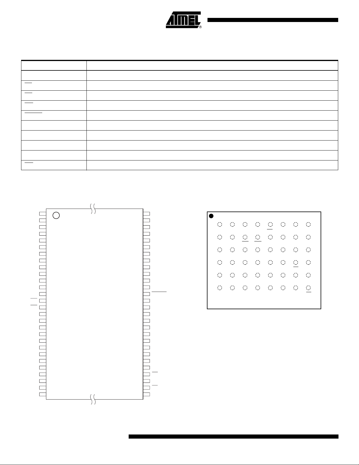
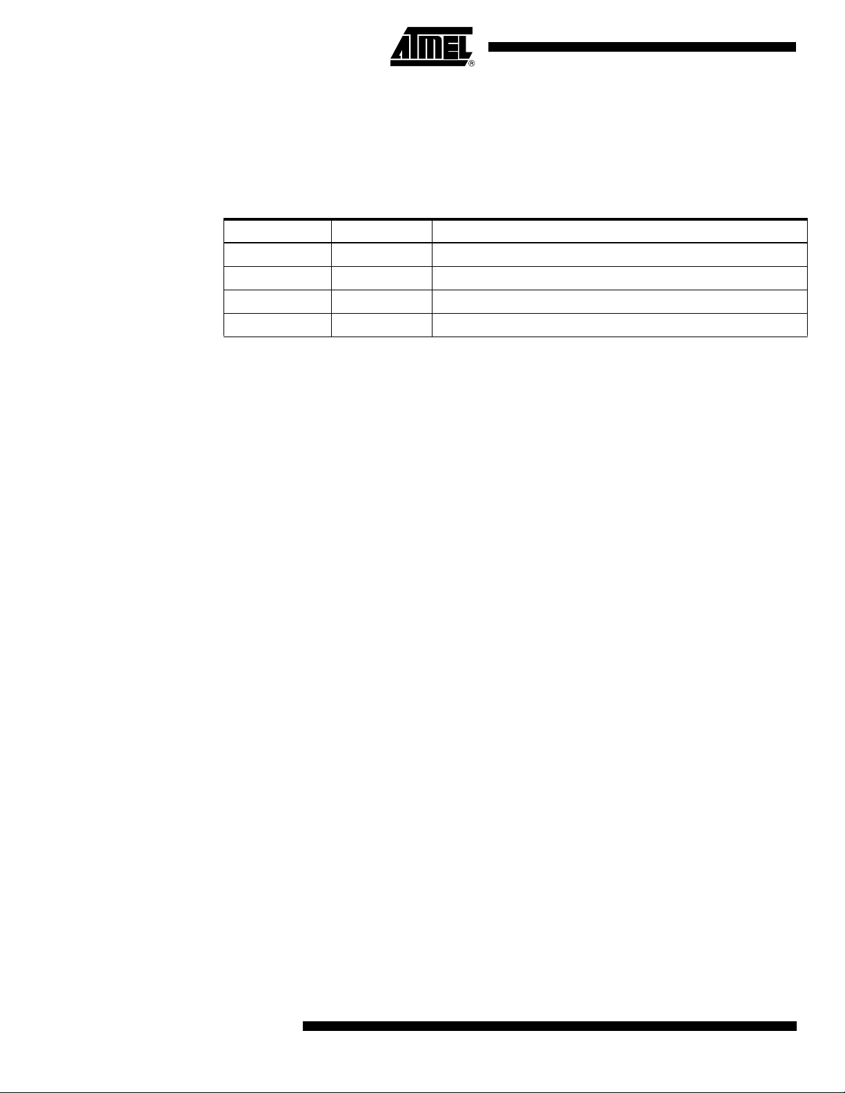
2. Pin Configurations
Pin Name Pin Function
A0 - A21 Addresses
CE
Chip Enable
OE
WE
RESET
Output Enable
Write Enable
Reset
VPP Write Protection and Power Supply for Accelerated Program Operations
I/O0 - I/O15 Data Inputs/Outputs
NC No Connect
VCCQ Output Power Supply
WP
2.1 56-lead TSOP Top View
A9
A8
NC
WE
WP
A7
A6
A5
A4
A3
A2
A1
NC
NC
1
2
3
4
5
6
7
8
9
10
11
12
13
14
15
16
17
18
19
20
21
22
23
24
25
26
27
28
A15
A14
A13
A12
A11
A10
A21
A20
VSS
VCC
A19
A18
A17
VSS
Write Protect
56
55
54
53
52
51
50
49
48
47
46
45
44
43
42
41
40
39
38
37
36
35
34
33
32
31
30
29
NC
A16
I/O15
I/O7
I/O14
I/O6
I/O13
I/O5
I/O12
I/O4
NC
NC
RESET
VPP
I/O11
I/O3
I/O10
I/O2
VCCQ
I/O9
I/O1
I/O8
I/O0
VCC
OE
VSS
CE
A0
2.2 48-ball CBGA – Top View
234567
1
A
A8
A11
A13
B
WE
A10
A14
C
A9
A12
A15
D
I/O5
I/O14
A16
E
I/O6
I/O15
VCCQ
F
I/O13
I/O7
GND
VPP
RST
A21
I/O11
I/O12
I/O4
WP
A18
A20
I/O2
I/O3
VCC
A19
A17
A6
I/O8
I/O9
I/O10
A7
A5
A3
CE
I/O0
I/O1
8
A4
A2
A1
A0
GND
OE
2
AT49BV640D(T)
3608A–FLASH–04/06
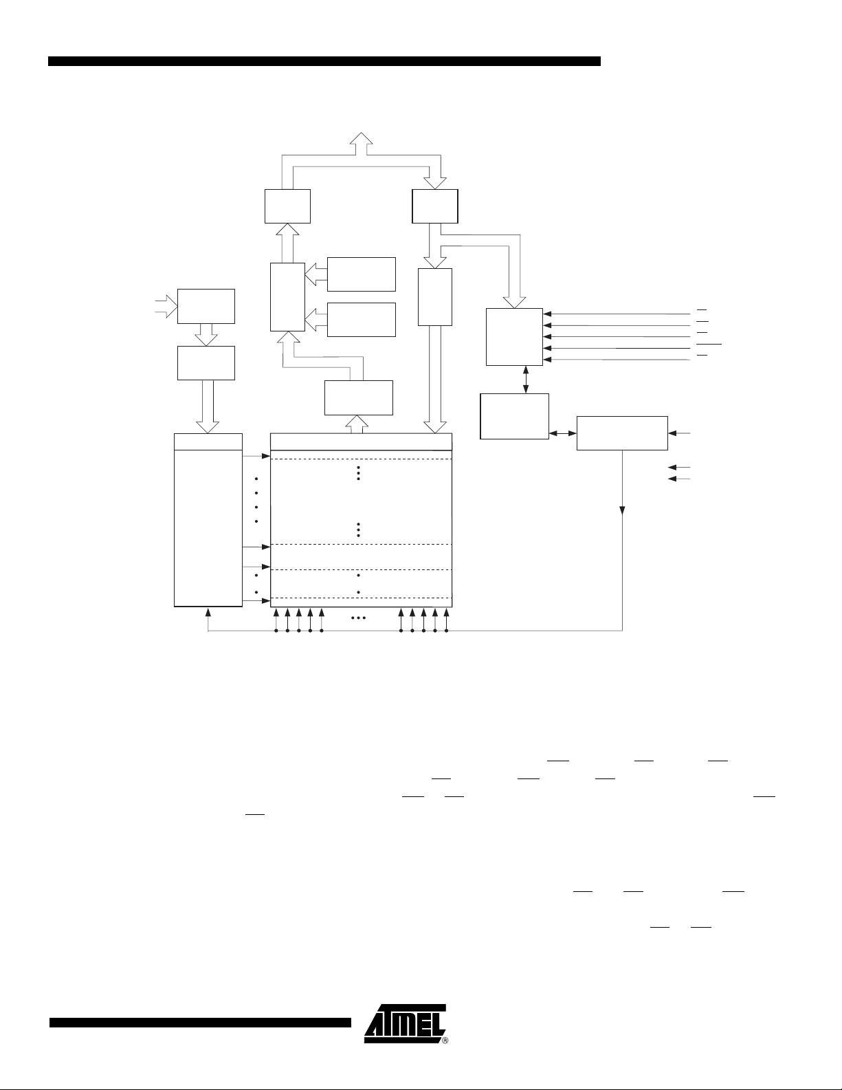
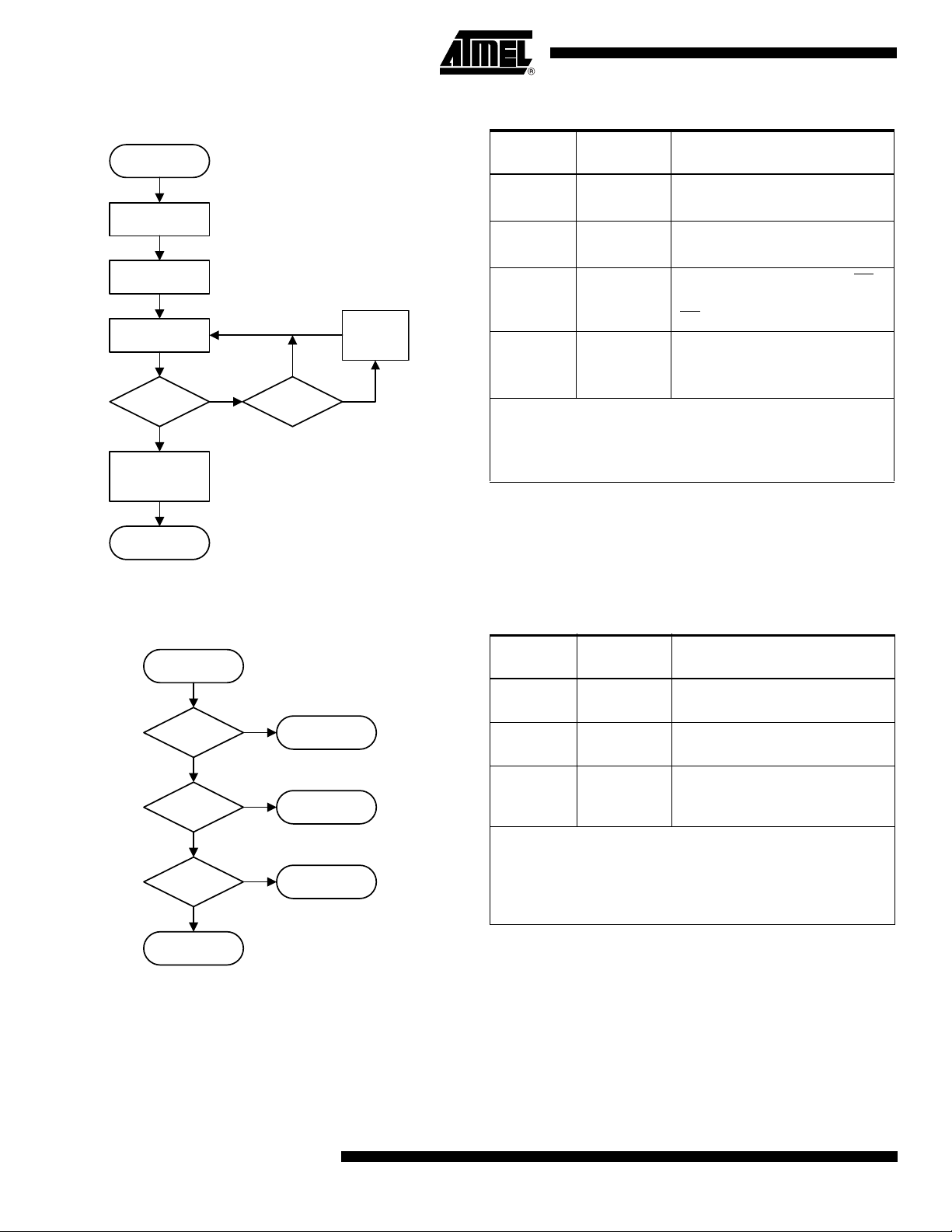
3. Block Diagram
AT49BV640D(T)
I/O0 - I/O15
A0 - A21
INPUT
BUFFER
ADDRESS
LATCH
Y-DECODER
X-DECODER
OUTPUT
BUFFER
OUTPUT
MULTIPLEXER
IDENTIFIER
REGISTER
STAT US
REGISTER
DATA
COMPARATOR
Y-GATING
MAIN
MEMORY
INPUT
BUFFER
DATA
REGISTER
COMMAND
REGISTER
WRITE STAT E
MACHINE
PROGRAM/ERASE
VOLTAGE SWITCH
CE
WE
OE
RESET
WP
VPP
VCC
GND
4. Device Operation
4.1 Command Sequences
When the device is first powered on, it will be in the read mode. Command sequences are
used to place the device in other operating modes such as program and erase. The command
sequences are written by applying a low pulse on the WE
applying a low-going pulse on the CE
on the first rising edge of the WE
the CE
affected by entering the command sequences.
4.2 Read
The AT49BV640D(T) is accessed like an EPROM. When CE and OE are low and WE is high,
the data stored at the memory location determined by the address pins are asserted on the
outputs. The outputs are put in the high impedance state whenever CE
dual-line control gives designers flexibility in preventing bus contention.
3608A–FLASH–04/06
input with CE low and OE high or by
input with WE low and OE high. The address is latched
or CE. Valid data is latched on the rising edge of the WE or
pulse, whichever occurs first. The addresses used in the command sequences are not
or OE is high. This
3

4.3 Reset
A RESET input pin is provided to ease some system applications. When RESET is at a logic
high level, the device is in its standard operating mode. A low level on the RESET
present device operation and puts the outputs of the device in a high-impedance state. When
a high level is reasserted on the RESET
4.4 Erase
Before a word can be reprogrammed it must be erased. The erased state of the memory bits is
a logical “1”. The individual sectors can be erased by using the Sector Erase command.
4.4.1 Sector Erase
The device is organized into 135 sectors (SA0 - SA134) that can be individually erased. The
Sector Erase command is a two-bus cycle operation. The sector address and the D0H Data
Input command are latched on the rising edge of WE
edge of WE
operation is internally controlled; it will automatically time to completion. The maximum time to
erase a sector is t
operation terminating immediately.
4.5 Word Programming
Once a memory sector is erased, it is programmed (to a logical “0”) on a word-by-word basis.
Programming is accomplished via the Internal Device command register and is a two-bus
cycle operation. The device will automatically generate the required internal program pulses.
pin halts the
pin, the device returns to read mode.
. The sector erase starts after the rising
of the second cycle provided the given sector has not been protected. The erase
. An attempt to erase a sector that has been protected will result in the
SEC
4.6 VPP Pin
Any commands except Read Status Register, Program Suspend and Program Resume written to the chip during the embedded programming cycle will be ignored. If a hardware reset
happens during programming, the data at the location being programmed will be corrupted.
Please note that a data “0” cannot be programmed back to a “1”; only erase operations can
convert “0”s to “1”s. Programming is completed after the specified t
gram status bit is a “1”, the device was not able to verify that the program operation was
performed successfully. The status register indicates the programming status. While the program sequence executes, status bit I/O7 is “0”.
The circuitry of the AT49BV640D(T) is designed so that the device cannot be programmed or
erased if the V
and erase operations can be performed. The VPP pin cannot be left floating.
voltage is less that 0.4V. When VPP is at 1.65V or above, normal program
PP
cycle time. If the pro-
BP
4
AT49BV640D(T)
3608A–FLASH–04/06
4.7 Read Status Register
The status register indicates the status of device operations and the success/failure of that
operation. The Read Status Register command causes subsequent reads to output data from
the status register until another command is issued. To return to reading from the memory,
issue a Read command.
The status register bits are output on I/O7 - I/O0. The upper byte, I/O15 - I/O8, outputs 00H
when a Read Status Register command is issued.
AT49BV640D(T)
The contents of the status register [SR7:SR0] are latched on the falling edge of OE
(whichever occurs last), which prevents possible bus errors that might occur if status register
contents change while being read. CE
or OE must be toggled with each subsequent status
read, or the status register will not indicate completion of a Program or Erase operation.
When the Write State Machine (WSM) is active, SR7 will indicate the status of the WSM; the
remaining bits in the status register indicate whether the WSM was successful in performing
the preferred operation (see Table 4-1).
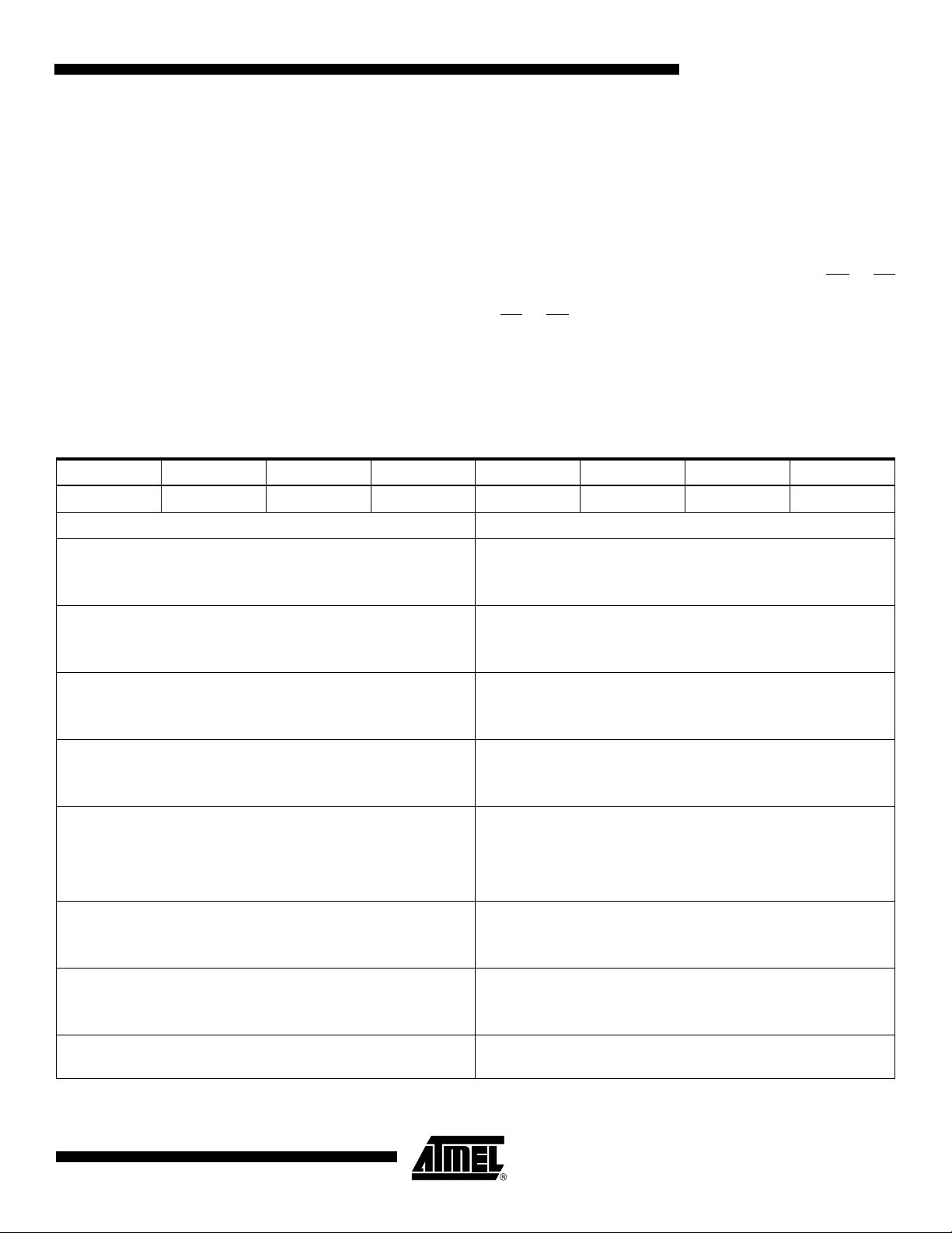
Table 4-1. Status Register Bit Definition
WSMS ESS ES PRS VPPS PSS SLS R
76543210
Notes
SR7 WRITE STATE MACHINE STATUS (WSMS)
1 = Ready
0 = Busy
SR6 = ERASE SUSPEND STATUS (ESS)
1 = Erase Suspended
0 = Erase In Progress/Completed
SR5 = ERASE STATUS (ES)
1 = Error in Sector Erase
0 = Successful Sector Erase
Check Write State Machine bit first to determine Word Program
or Sector Erase completion, before checking program or erase
status bits.
When Erase Suspend is issued, WSM halts execution and sets
both WSMS and ESS bits to “1” – ESS bit remains set to “1” until
an Erase Resume command is issued.
When this bit is set to “1”, WSM has applied the max number of
erase pulses to the sector and is still unable to verify successful
sector erasure.
or CE
SR4 = PROGRAM STATUS (PRS)
1 = Error in Programming
0 = Successful Programming
SR3 = VPP STATUS (VPPS)
1 = VPP Low Detect, Operation Abort
0 = VPP OK
SR2 = PROGRAM SUSPEND STATUS (PSS)
1 = Program Suspended
0 = Program in Progress/Completed
SR1 = SECTOR LOCK STATUS (SLS)
1 = Prog/Erase attempted on a locked sector; Operation aborted.
0 = No operation to locked sectors
SR0 = Reserved for Future Enhancements (R)
Note: 1. A Command Sequence Error is indicated when SR1, SR3, SR4 and SR5 are set.
3608A–FLASH–04/06
When this bit is set to “1”, WSM has attempted but failed to
program a word
The V
level. The WSM interrogates V
Erase command sequences have been entered and informs the
system if VPP has not been switched on. The VPP is also checked
before the operation is verified by the WSM.
When Program Suspend is issued, WSM halts execution and
sets both WSMS and PSS bits to “1”. PSS bit remains set to “1”
until a Program Resume command is issued.
If a Program or Erase operation is attempted to one of the locked
sectors, this bit is set by the WSM. The operation specified is
aborted and the device is returned to read status mode.
This bit is reserved for future use and should be masked out
when polling the status register.
status bit does not provide continuous indication of VPP
PP
level only after the Program or
PP
5

4.8 Clear Status Register
The WSM can set status register bits 1 through 7 and can clear bits 2, 6 and 7; but, the WSM
cannot clear status register bits 1, 3, 4 or 5. Because bits 1, 3, 4 and 5 indicate various error
conditions, these bits can be cleared only through the Clear Status Register command. By
allowing the system software to control the resetting of these bits, several operations may be
performed (such as cumulatively programming several addresses or erasing multiple sectors
in sequence) before reading the status register to determine if an error occurred during those
operations. The status register should be cleared before beginning another operation. The
Read command must be issued before data can be read from the memory array. The status
register can also be cleared by resetting the device.
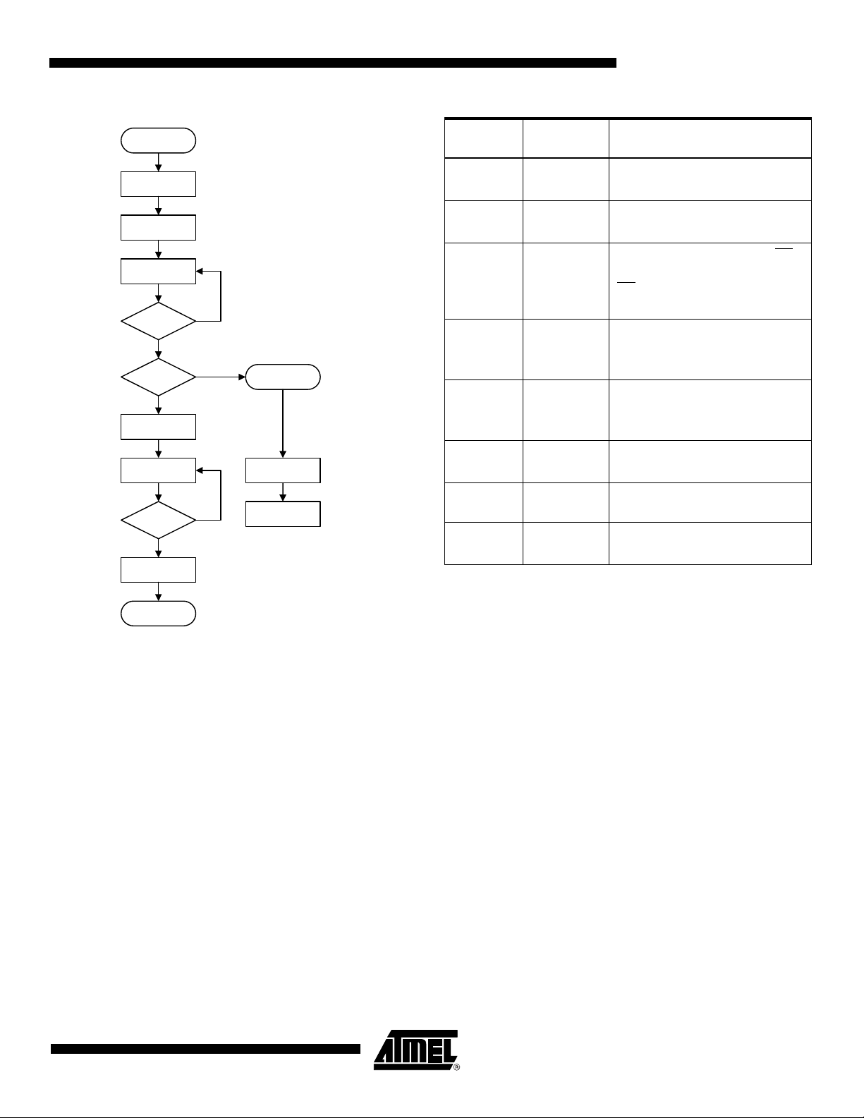
4.9 Flexible Sector Protection
The AT49BV640D(T) offers two sector protection modes, the Softlock and the Hardlock. The
Softlock mode is optimized as sector protection for sectors whose content changes frequently.
The Hardlock protection mode is recommended for sectors whose content changes infrequently. Once either of these two modes is enabled, the contents of the selected sector is
read-only and cannot be erased or programmed. Each sector can be independently programmed for either the Softlock or Hardlock sector protection mode. At power-up and reset, all
sectors have their Softlock protection mode enabled.
4.9.1 Softlock and Unlock
The Softlock protection mode can be disabled by issuing a two-bus cycle Unlock command to
the selected sector. Once a sector is unlocked, its contents can be erased or programmed. To
enable the Softlock protection mode, a two-bus cycle Softlock command must be issued to the
selected sector.
4.9.2 Hardlock and Write Protect (WP
The Hardlock sector protection mode operates in conjunction with the Write Protection (WP
pin. The Hardlock sector protection mode can be enabled by issuing a two-bus cycle Hardlock
software command to the selected sector. The state of the Write Protect pin affects whether
the Hardlock protection mode can be overridden.
• When the WP pin is low and the Hardlock protection mode is enabled, the sector cannot be
unlocked and the contents of the sector is read-only.
• When the WP pin is high, the Hardlock protection mode is overridden and the sector can be
unlocked via the Unlock command.
To disable the Hardlock sector protection mode, the chip must be either reset or power cycled.
)
)
6
AT49BV640D(T)
3608A–FLASH–04/06
AT49BV640D(T)
Table 4-2. Hardlock and Softlock Protection Configurations in Conjunction with WP
Erase/
Hard-
V
PP
/5V 0 0 0 Yes No sector is locked
V
CC
WP
lock
VCC/5V 0 0 1 No
V
/5V 0 1 1 No
CC
/5V 1 0 0 Yes No sector is locked.
V
CC
VCC/5V 1 0 1 No
V
/5V 1 1 0 Yes
CC
V
/5V 1 1 1 No
CC
V
IL
xx x No
Soft-
lock
Prog
Allowed? Comments
Sector is Softlocked. The Unlock
command can unlock the sector.
Hardlock protection mode is
enabled. The sector cannot be
unlocked.
Sector is Softlocked. The Unlock
command can unlock the sector.
Hardlock protection mode is
overridden and the sector is not
locked.
Hardlock protection mode is
overridden and the sector can be
unlocked via the Unlock command.
Erase and Program Operations
cannot be performed.
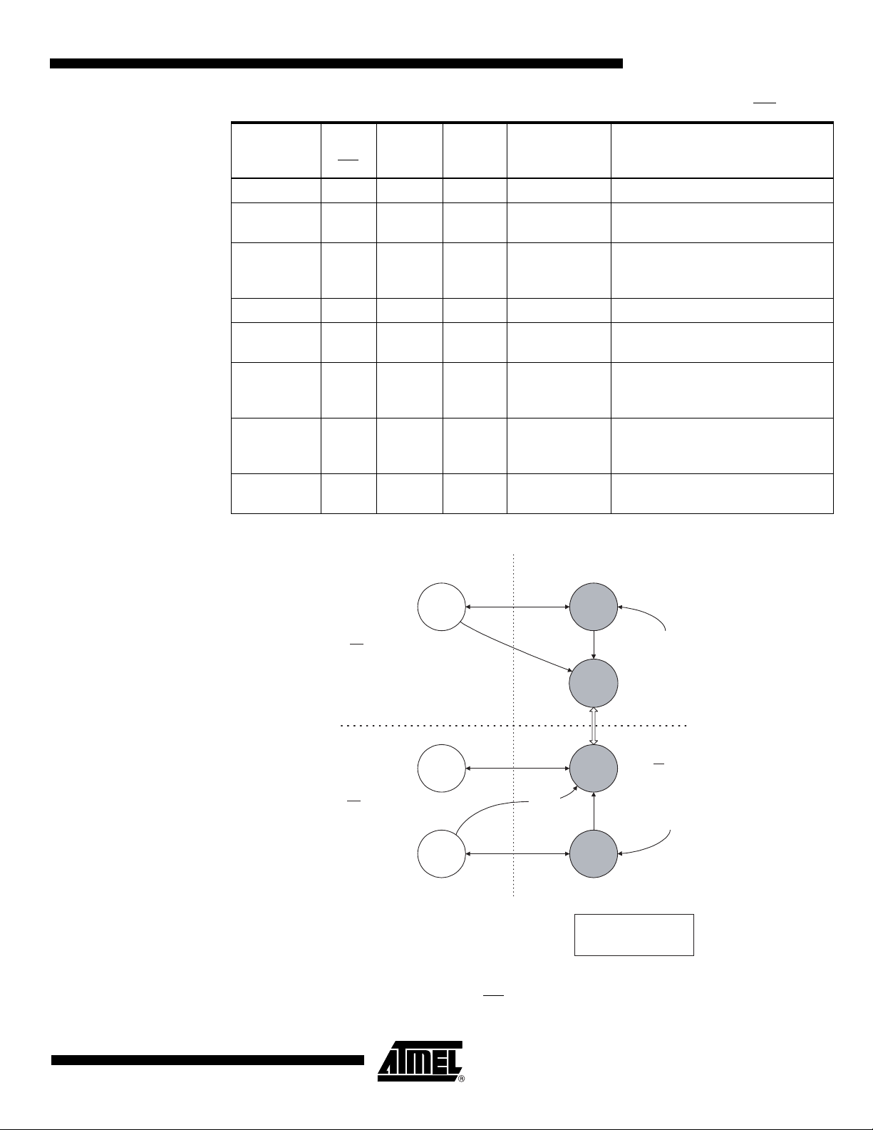
Figure 4-1. Sector Locking State Diagram
UNLOCKED LOCKED
60h/
D0h
6
0
60h/D0h
60h/
D0h
h
/
2
F
WP = V
WP = V
[000] [001]
=0
IL
[110]
=1
IH
[100]
60h/01h
h
60h/
2Fh
60h/
01h
60h/
2Fh
[011]
60h/
01h
[111]
[101]
60h/D0h = Unlock Comman d
60h/01h = Softlock Command
60h/2Fh = Hardlock Command
Power-Up/Rese t
Default
Hardlocked
Hardlocked is disabled by
WP = V
60h/
Power-Up/Rese t
2Fh
Default
IH
3608A–FLASH–04/06
Note: 1. The notation [X, Y, Z] denotes the locking state of a sector. The current locking state of a
sector is defined by the state of WP
and the two bits of the sector-lock status D[1:0].
7
4.9.3 Sector Protection Detection
A software method is available to determine if the sector protection Softlock or Hardlock features are enabled. When the device is in the software product identification mode a read from
the I/O0 and I/O1 at address location 00002H within a sector will show if the sector is
unlocked, softlocked, or hardlocked.
Table 4-3. Sector Protection Status
I/O1 I/O0 Sector Protection Status
0 0 Sector Not Locked
0 1 Softlock Enabled
1 0 Hardlock Enabled
1 1 Both Hardlock and Softlock Enabled
4.10 Erase Suspend/Erase Resume
The Erase Suspend command allows the system to interrupt a sector erase operation and
then program or read data from a different sector within the memory. After the Erase Suspend
command is given, the device requires a maximum time of 15 µs to suspend the erase operation. After the erase operation has been suspended, the system can then read data or
program data to any other sector within the device. An address is not required during the
Erase Suspend command. During a sector erase suspend, another sector cannot be erased.
To resume the sector erase operation, the system must write the Erase Resume command.
The Erase Resume command is a one-bus cycle command. The only valid commands while
erase is suspended are Read Status Register, Product ID Entry, CFI Query, Program, Program Resume, Erase Resume, Sector Softlock/Hardlock, and Sector Unlock.
4.11 Program Suspend/Program Resume
The Program Suspend command allows the system to interrupt a programming operation and
then read data from a different word within the memory. After the Program Suspend command
is given, the device requires a maximum of 10 µs to suspend the programming operation. After
the programming operation has been suspended, the system can then read from any other
word within the device. An address is not required during the program suspend operation. To
resume the programming operation, the system must write the Program Resume command.
The program suspend and resume are one-bus cycle commands. The command sequence for
the erase suspend and program suspend are the same, and the command sequence for the
erase resume and program resume are the same. Read, Read Status Register, Product ID
Entry, Program Resume are valid commands during a Program Suspend.
4.12 Product Identification
The product identification mode identifies the device and manufacturer as Atmel. It may be
accessed by a software operation. For details, see “Operating Modes” on page 21.
8
AT49BV640D(T)
3608A–FLASH–04/06

4.13 128-bit Protection Register
The AT49BV640D(T) contains a 128-bit register that can be used for security purposes in system design. The protection register is divided into two 64-bit blocks. The two blocks are
designated as block A and block B. The data in block A is non-changeable and is programmed
at the factory with a unique number. The data in block B is programmed by the user and can
be locked out such that data in the sector cannot be reprogrammed. To program block B in the
protection register, the two-bus cycle Program Protection Register command must be used as
shown in the “Command Definition Table” on page 15. To lock out block B, the two-bus cycle
Lock Protection Register command must be used as shown in the “Command Definition
Table”. Data bit D1 must be zero during the second bus cycle. To determine whether block B
is locked out, use the status of block B protection command. If data bit D1 is zero, block B is
locked. If data bit D1 is one, block B can be reprogrammed. Please see the “Protection Regis-
ter Addressing Table” on page 16 for the address locations in the protection register. To read
the protection register, the Product ID Entry command is given followed by a normal read
operation from an address within the protection register. After determining whether block B is
protected or not, or reading the protection register, the Read command must be given to return
to the read mode.
4.14 Common Flash Interface (CFI)
CFI is a published, standardized data structure that may be read from a flash device. CFI
allows system software to query the installed device to determine the configurations, various
electrical and timing parameters, and functions supported by the device. CFI is used to allow
the system to learn how to interface to the flash device most optimally. The two primary benefits of using CFI are ease of upgrading and second source availability. The command to enter
the CFI Query mode is a one-bus cycle command which requires writing data 98h to any
address. The CFI Query command can be written when the device is ready to read data or can
also be written when the part is in the product ID mode. Once in the CFI Query mode, the system can read CFI data at the addresses given in “Common Flash Interface Definition Table”
on page 26. To return to the read mode, the read command should be issued.
AT49BV640D(T)
4.15 Hardware Data Protection
Hardware features protect against inadvertent programs to the AT49BV640D(T) in the following ways: (a) V
erase functions are inhibited. (b) V
level, the device will automatically time-out 10 ms (typical) before programming. (c) Program
inhibit: holding any one of OE
inhibit: V
is less than V
PP
4.16 Input Levels
While operating with a 2.65V to 3.6V power supply, the address inputs and control inputs (OE,
CE
and WE) may be driven from 0 to 5.5V without adversely affecting the operation of the
device. The I/O lines can be driven from 0 to V
4.17 Output Levels
For the AT49BV640D(T), output high levels are equal to V
3.6V output levels, V
3608A–FLASH–04/06
sense: if VCC is below 1.8V (typical), the device is reset and the program and
CC
power-on delay: once VCC has reached the VCC sense
CC
low, CE high or WE high inhibits program cycles. (d) Program
.
ILPP
+ 0.6V.
CCQ
- 0.1V (not VCC). For 2.65V to
CCQ
must be tied to VCC.
CCQ
9
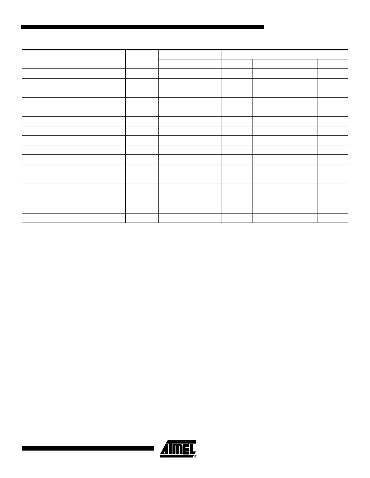
4.18 Word Program Flowchart
Start
Wri te 40,
Any Addr ess
Wr ite D ata,
Wor d Ad dr es s
Read-Status
Regi ster
SR7 =
1
Full Status
Check
(If Desired)
Progr am
Complete
(Set up)
(Confirm)
0
No
Suspend?
Program
Suspend
Loop
Ye s
4.19 Word Program Procedure
Bus
Operation Command Comments
Write
Program
Setup
Write Data
Read None
Idle None
Repeat for subsequent Word Program operations.
Full status register check can be done after each program, or
after a sequence of program operations.
Write FF after the last operation to set to the Read state.
Data = 40
Addr = Any Address
Data = Data to program
Addr = Location to program
Status register data: Toggle CE
or
to update status register
OE
Check SR7
1 = WSM Ready
0 = WSM Busy
4.20 Full Status Check Flowchart
Read Status
Regi ster
SR3 =
0
SR4 =
0
SR1 =
0
Program
Successful
1 V
1
1
Range
PP
Error
Program
Error
Device
Protect Er ror
4.21 Full Status Check Procedure
Bus
Operation Command Comments
Idle None
Idle None
Idle None
SR3 MUST be cleared before the Write State Machine allows
further program attempts.
If an error is detected, clear the status register before
continuing operations – only the Clear Status Register
command clears the status register error bits.
Check SR3:
Error
1 = V
PP
Check SR4:
1 = Data Program Error
Check SR1:
1 = Sector locked; operation
aborted
10
AT49BV640D(T)
3608A–FLASH–04/06
AT49BV640D(T)
4.22 Program Suspend/Resume Flowchart
Start
Wr ite B0
Any Address
Wr ite 70
Any Address
Read Status
Register
SR7 =
SR2 =
Wr ite FF
Read
Data
Done
Reading
Wr ite D 0
Any Address
1
1
Ye s
(Prog ram Suspend)
(Read S tatus)
0
0
Completed
(ReadArray)
No
(Pr ogramResu me)
Progr am
Wr ite F F
Read
Data
(Re ad
Array)
4.23 Program Suspend/Resume Procedure
Bus
Operation Command Comments
Write
Write
Program
Suspend
Read
Status
Read None
Idle None
Idle None
Write Read Array
Read None
Write
Program
Resume
Data = B0
Addr = Any address
Data = 70
Addr = Any address
Status register data: Toggle CE
or
to update status register
OE
Addr = Any address
Check SR7
1 = WSM Ready
0 = WSM Busy
Check SR2
1 = Program suspended
0 = Program completed
Data = FF
Addr = Any address
Read data from any word in the
memory
Data = D0
Addr = Any address
Progr am
Resumed
3608A–FLASH–04/06
11

4.24 Sector Erase Flowchart
Start
Wri te 20,
Addr ess
Any
Wri te D 0,
Addr ess
Sector
Read Status
Regist er
SR7 =
Full Er ase
Status Check
(IfDesired)
Sector
Complete
(Erase)
Sector
(Erase Confirm)
0 Ye s
1
Erase
No
Suspend
Eras e
Suspend
Eras e
Loop
4.25 Sector Erase Procedure
Bus
Operation Command Comments
Sector
Write
Erase
Setup
Write
Erase
Confirm
Read None
Idle None
Repeat for subsequent sector erasures.
Full status register check can be done after each sector erase,
or after a sequence of sector erasures.
Write FF after the last operation to enter read mode.
Data = 20
Addr = Any Address
Data = D0
Addr = Sector to be erased (SA)
Status register data: Toggle CE
or
to update status register data
OE
Check SR7
1 = WSMS Ready
0 = WSMS Busy
4.26 Full Erase Status Check Flowchart
Read Status
Regist er
SR3 =
SR4, SR5
SR5 =
SR1 =
Sector
Successful
0
=
0
0
0
Erase
1
1,1
1
1
VPPRange
Error
Command
Sequenc e Error
Sector
Eras e
Error
Sector
Lock ed
Error
4.27 Full Erase Status Check Procedure
Bus
Operation Command Comments
Idle None
Idle None
Idle None
Idle None
SR1, SR3 must be cleared before the Write State Machine
allows further erase attempts.
Only the Clear Status Register command clears SR1, SR3,
SR4, SR5.
If an error is detected, clear the status register before
attempting an erase retry or other error recovery.
Check SR3:
1 = V
Range Error
PP
Check SR4, SR5:
Both 1 = Command Sequence
Error
Check SR5:
1 = Sector Erase Error
Check SR1:
1 = Attempted erase of locked
sector; erase aborted.
12
AT49BV640D(T)
3608A–FLASH–04/06

AT49BV640D(T)
4.28 Erase Suspend/Resume Flowchart
Star t
(Rea d A rray)
(E ra se R esu m e)
Write B 0,
Any Addr ess
Write 70,
Any Addr ess
Read-Status
Regis ter
SR7 =
SR6 =
Wr it e F F
ReadData
Done
Reading
Write D 0,
Any Addr ess
1
1
1
(Erase Suspend)
(Read-Status)
0
0
0
Erase
Completed
Write FF
(Read-Array)
4.29 Erase Suspend/Resume Procedure
Bus
Operation Command Comments
Write
Write
Erase
Suspend
Read
Status
Read None
Idle None
Idle None
Write
Read or
Write
Write
Read or
Program
None
Program
Resume
Data = B0
Addr = Any address
Data = 70
Addr = Any address
Status register data: Toggle CE
or
to update status register
OE
Addr = Any address
Check SR7
1 = WSM Ready
0 = WSM Busy
Check SR6
1 = Erase suspended
0 = Erase completed
Data = FF or 40
Addr = Any address
Read or program data from/to
sector other than the one being
erased
Data = D0
Addr = Any address
Erase
Resumed
Read Array
Data
3608A–FLASH–04/06
13

4.30 Protection Register Programming Flowchart
Start
4.31 Protection Register Programming Procedure
Bus
Operation Command Comments
Wri te C0,
Any Address
Wri te PR
Address Data
Read-Status
Register
SR7 =
Full-Status
Chec k
(If Des ired)
Progr am
Complete
(Program-Setup)
(Confirm Data )
0
1
4.32 Full Status Check Flowchart
Read Status
Register Data
Write
Write
Program
PR Setup
Protection
Program
Data = C0
Addr = Any Address
Data = Data to Program
Addr = Location to Program
Status register data: Toggle CE
Read None
or
to update status register data
OE
Check SR7
Idle None
1 = WSMS Ready
0 = WSMS Busy
Program Protection Register operation addresses must be
within the protection register address space. Addresses
outside this space will return an error.
Repeat for subsequent programming operations.
Full status register check can be done after each program, or
after a sequence of program operations.
Write FF after the last operation to return to the Read mode.
4.33 Full Status Check Procedure
Bus
Operation Command Comments
SR3, SR4
0
SR1, SR4
0
SR1, SR4
0
Program
Successful
1, 1
= VPPRange Error
0, 1
1, 1
Progr am Er ror
Regi ster Locked;
Progr am Abor ted
=
=
Idle None
Idle None
Check SR1, SR3, SR4:
0,1,1 = V
Range Error
PP
Check SR1, SR3, SR4:
0,0,1 = Programming Error
Check SR1, SR3, SR4:
Idle None
1, 0,1 = Sector locked; operation
aborted
SR3 must be cleared before the Write State Machine allows
further program attempts.
Only the Clear Status Register command clears SR1, SR3,
SR4.
If an error is detected, clear the status register before
attempting a program retry or other error recovery.
14
AT49BV640D(T)
3608A–FLASH–04/06
5. Command Definition Table
AT49BV640D(T)
1st Bus Cycle 2nd Bus Cycle 3rd Bus Cycle
Addr Data Addr Data Addr Data
Command Sequence
Bus
Cycles
Read 1 XX FF
Sector Erase 2 XX 20 SA
Word Program 2 XX 40/10 Addr D
Dual Word Program
(3)
3 XX E0 Addr0 D
(2)
D0
IN0
IN
Addr1 D
IN1
Erase/Program Suspend 1 XX B0
Erase/Program Resume 1 XX D0
Product ID Entry
Sector Softlock 2 XX 60 SA
Sector Hardlock 2 XX 60 SA
Sector Unlock 2 XX 60 SA
Read Status Register 2 XX 70 XX D
(4)
1XX90
(2)
(2)
(2)
01
2F
D0
OUT
(5)
Clear Status Register 1 XX 50
Program Protection Register (Block B) 2 XX C0 Addr
(6)
D
IN
Lock Protection Register (Block B) 2 XX C0 80 FFFD
Status of Protection Register (Block B) 2 XX 90 80 D
OUT1
(7)
CFI Query 1 XX 98
Notes: 1. The DATA FORMAT shown for each bus cycle is as follows; I/O7 - I/O0 (Hex). I/O15 - I/O8 are don’t care. The ADDRESS FORMAT
shown for each bus cycle is as follows: A7 - A0 (Hex). Address A21 through A8 are don’t care.
2. SA = sector address. Any word address within a sector can be used to designate the sector address (see pages 17 - 20 for details).
3. This fast programming option enables the user to program two words in parallel only when V
Addr1, of the two words, D
and D
IN0
, must only differ in address A0. This command should be used during manufacturing pur-
IN1
= 9.5V. The addresses, Addr0 and
PP
poses only.
4. During the second bus cycle, the manufacturer code is read from address 000000H, the device code is read from address
000001H, and the data in the protection register is read from addresses 000081H - 000088H.
5. The status register bits are output on I/O7 - I/O0.
6. Any address within the user programmable protection register region. Address locations are shown on the “Protection Register
Addressing Table” on page 16.
7. If data bit D1 is “0”, block B is locked. If data bit D1 is “1”, block B can be reprogrammed.
3608A–FLASH–04/06
15

6. Absolute Maximum Ratings*
Temperature under Bias ................................ -55°C to +125°C
Storage Temperature ..................................... -65°C to +150°C
All Input Voltages Except V
(including NC Pins)
with Respect to Ground ...................................-0.6V to +6.25V
All Output Voltages
with Respect to Ground ...........................-0.6V to V
V
Input Voltage
PP
with Respect to Ground .....................................-0.6V to 10.0V
PP
CCQ
+ 0.6V
*NOTICE: Stresses beyond those listed under “Absolute
Maximum Ratings” may cause permanent damage to the device. This is a stress rating only and
functional operation of the device at these or any
other conditions beyond those indicated in the
operational sections of this specification is not
implied. Exposure to absolute maximum rating
conditions for extended periods may affect device
reliability.
7. Protection Register Addressing Table
AddressUseBlockA8A7A6A5A4A3A2A1A0
81FactoryA 010000001
82FactoryA 010000010
83FactoryA 010000011
84FactoryA 010000100
85UserB 010000101
86UserB 010000110
87UserB 010000111
88UserB 010001000
Note: All address lines not specified in the above table must be “0” when accessing the protection register, i.e., A21 - A8 = 0.
16
AT49BV640D(T)
3608A–FLASH–04/06

AT49BV640D(T)
8. Memory Organization –
AT49BV640D
Address Range
Sector Size (Words)
SA0 4K 00000 - 00FFF
SA1 4K 01000 - 01FFF
SA2 4K 02000 - 02FFF
SA3 4K 03000 - 03FFF
SA4 4K 04000 - 04FFF
SA5 4K 05000 - 05FFF
SA6 4K 06000 - 06FFF
SA7 4K 07000 - 07FFF
SA8 32K 08000 - 0FFFF
SA9 32K 10000 - 17FFF
SA10 32K 18000 - 1FFFF
SA11 32K 20000 - 27FFF
SA12 32K 28000 - 2FFFF
SA13 32K 30000 - 37FFF
SA14 32K 38000 - 3FFFF
SA15 32K 40000 - 47FFF
SA16 32K 48000 - 4FFFF
SA17 32K 50000 - 57FFF
SA18 32K 58000 - 5FFFF
SA19 32K 60000 - 67FFF
SA20 32K 68000 - 6FFFF
SA21 32K 70000 - 77FFF
SA22 32K 78000 - 7FFFF
SA23 32K 80000 - 87FFF
SA24 32K 88000 - 8FFFF
SA25 32K 90000 - 97FFF
SA26 32K 98000 - 9FFFF
SA27 32K A0000 - A7FFF
SA28 32K A8000 - AFFFF
SA29 32K B0000 - B7FFF
SA30 32K B8000 - BFFFF
SA31 32K C0000 - C7FFF
SA32 32K C8000 - CFFFF
SA33 32K D0000 - D7FFF
SA34 32K D8000 - DFFFF
(A21 - A0)
x16
8. Memory Organization –
AT49BV640D (Continued)
Sector Size (Words)
SA35 32K E0000 - E7FFF
SA36 32K E8000 - EFFFF
SA37 32K F0000 - F7FFF
SA38 32K F8000 - FFFFF
SA39 32K 100000 - 107FFF
SA40 32K 108000 - 10FFFF
SA41 32K 110000 - 117FFF
SA42 32K 118000 - 11FFFF
SA43 32K 120000 - 127FFF
SA44 32K 128000 - 12FFFF
SA45 32K 130000 - 137FFF
SA46 32K 138000 - 13FFFF
SA47 32K 140000 - 147FFF
SA48 32K 148000 - 14FFFF
SA49 32K 150000 - 157FFF
SA50 32K 158000 - 15FFFF
SA51 32K 160000 - 167FFF
SA52 32K 168000 - 16FFFF
SA53 32K 170000 - 177FFF
SA54 32K 178000 - 17FFFF
SA55 32K 180000 - 187FFF
SA56 32K 188000 - 18FFFF
SA57 32K 190000 - 197FFF
SA58 32K 198000 - 19FFFF
SA59 32K 1A0000 - 1A7FFF
SA60 32K 1A8000 - 1AFFFF
SA61 32K 1B0000 - 1B7FFF
SA62 32K 1B8000 - 1BFFFF
SA63 32K 1C0000 - 1C7FFF
SA64 32K 1C8000 - 1CFFFF
SA65 32K 1D0000 - 1D7FFF
SA66 32K 1D8000 - 1DFFFF
SA67 32K 1E0000 - 1E7FFF
SA68 32K 1E8000 - 1EFFFF
SA69 32K 1F0000 - 1F7FFF
SA70 32K 1F8000 - 1FFFFF
Address Range
(A21 - A0)
x16
3608A–FLASH–04/06
17

8. Memory Organization –
8. Memory Organization –
AT49BV640D (Continued)
x16
Sector Size (Words)
SA71 32K 200000 - 207FFF
SA72 32K 208000 - 20FFFF
SA73 32K 210000 - 217FFF
SA74 32K 218000 - 21FFFF
SA75 32K 220000 - 227FFF
SA76 32K 228000 - 22FFFF
SA77 32K 230000 - 237FFF
SA78 32K 238000 - 23FFFF
SA79 32K 240000 - 247FFF
SA80 32K 248000 - 24FFFF
SA81 32K 250000 - 257FFF
SA82 32K 258000 - 25FFFF
SA83 32K 260000 - 267FFF
SA84 32K 268000 - 26FFFF
SA85 32K 270000 - 277FFF
SA86 32K 278000 - 27FFFF
SA87 32K 280000 - 287FFF
SA88 32K 288000 - 28FFFF
SA89 32K 290000 - 297FFF
SA90 32K 298000 - 29FFFF
SA91 32K 2A0000 - 2A7FFF
SA92 32K 2A8000 - 2AFFFF
SA93 32K 2B0000 - 2B7FFF
SA94 32K 2B8000 - 2BFFFF
SA95 32K 2C0000 - 2C7FFF
SA96 32K 2C8000 - 2CFFFF
SA97 32K 2D0000 - 2D7FFF
SA98 32K 2D8000 - 2DFFFF
SA99 32K 2E0000 - 2E7FFF
SA100 32K 2E8000 - 2EFFFF
SA101 32K 2F0000 - 2F7FFF
SA102 32K 2F8000 - 2FFFFF
Address Range
(A21 - A0)
AT49BV640D (Continued)
x16
Sector Size (Words)
SA103 32K 300000 - 307FFF
SA104 32K 308000 - 30FFFF
SA105 32K 310000 - 317FFF
SA106 32K 318000 - 31FFFF
SA107 32K 320000 - 327FFF
SA108 32K 328000 - 32FFFF
SA109 32K 330000 - 337FFF
SA110 32K 338000 - 33FFFF
SA111 32K 340000 - 347FFF
SA112 32K 348000 - 34FFFF
SA113 32K 350000 - 357FFF
SA114 32K 358000 - 35FFFF
SA115 32K 360000 - 367FFF
SA116 32K 368000 - 36FFFF
SA117 32K 370000 - 377FFF
SA118 32K 378000 - 37FFFF
SA119 32K 380000 - 387FFF
SA120 32K 388000 - 38FFFF
SA121 32K 390000 - 397FFF
SA122 32K 398000 - 39FFFF
SA123 32K 3A0000 - 3A7FFF
SA124 32K 3A8000 - 3AFFFF
SA125 32K 3B0000 - 3B7FFF
SA126 32K 3B8000 - 3BFFFF
SA127 32K 3C0000 - 3C7FFF
SA128 32K 3C8000 - 3CFFFF
SA129 32K 3D0000 - 3D7FFF
SA130 32K 3D8000 - 3DFFFF
SA131 32K 3E0000 - 3E7FFF
SA132 32K 3E8000 - 3EFFFF
SA133 32K 3F0000 - 3F7FFF
SA134 32K 3F8000 - 3FFFFF
Address Range
(A21 - A0)
18
AT49BV640D(T)
3608A–FLASH–04/06

AT49BV640D(T)
9. Memory Organization –
AT49BV640DT
Address Range
Sector Size (Words)
SA0 32K 00000 - 07FFF
SA1 32K 08000 - 0FFFF
SA2 32K 10000 - 17FFF
SA3 32K 18000 - 1FFFF
SA4 32K 20000 - 27FFF
SA5 32K 28000 - 2FFFF
SA6 32K 30000 - 37FFF
SA7 32K 38000 - 3FFFF
SA8 32K 40000 - 47FFF
SA9 32K 48000 - 4FFFF
SA10 32K 50000 - 57FFF
SA11 32K 58000 - 5FFFF
SA12 32K 60000 - 67FFF
SA13 32K 68000 - 6FFFF
SA14 32K 70000 - 77FFF
SA15 32K 78000 - 7FFFF
SA16 32K 80000 - 87FFF
SA17 32K 88000 - 8FFFF
SA18 32K 90000 - 97FFF
SA19 32K 98000 - 9FFFF
SA20 32K A0000 - A7FFF
SA21 32K A8000 - AFFFF
SA22 32K B0000 - B7FFF
SA23 32K B8000 - BFFFF
SA24 32K C0000 - C7FFF
SA25 32K C8000 - CFFFF
SA26 32K D0000 - D7FFF
SA27 32K D8000 - DFFFF
SA28 32K E0000 - E7FFF
SA29 32K E8000 - EFFFF
SA30 32K F0000 - F7FFF
SA31 32K F8000 - FFFFF
SA32 32K 100000 - 107FFF
SA33 32K 108000 - 10FFFF
SA34 32K 110000 - 117FFF
SA35 32K 118000 - 11FFFF
(A21 - A0)
x16
9. Memory Organization –
AT49BV640DT (Continued)
Sector Size (Words)
SA36 32K 120000 - 127FFF
SA37 32K 128000 - 12FFFF
SA38 32K 130000 - 137FFF
SA39 32K 138000 - 13FFFF
SA40 32K 140000 - 147FFF
SA41 32K 148000 - 14FFFF
SA42 32K 150000 - 157FFF
SA43 32K 158000 - 15FFFF
SA44 32K 160000 - 167FFF
SA45 32K 168000 - 16FFFF
SA46 32K 170000 - 177FFF
SA47 32K 178000 - 17FFFF
SA48 32K 180000 - 187FFF
SA49 32K 188000 - 18FFFF
SA50 32K 190000 - 197FFF
SA51 32K 198000 - 19FFFF
SA52 32K 1A0000 - 1A7FFF
SA53 32K 1A8000 - 1AFFFF
SA54 32K 1B0000 - 1B7FFF
SA55 32K 1B8000 - 1BFFFF
SA56 32K 1C0000 - 1C7FFF
SA57 32K 1C8000 - 1CFFFF
SA58 32K 1D0000 - 1D7FFF
SA59 32K 1D8000 - 1DFFFF
SA60 32K 1E0000 - 1E7FFF
SA61 32K 1E8000 - 1EFFFF
SA62 32K 1F0000 - 1F7FFF
SA63 32K 1F8000 - 1FFFFF
SA64 32K 200000 - 207FFF
SA65 32K 208000 - 20FFFF
SA66 32K 210000 - 217FFF
SA67 32K 218000 - 21FFFF
SA68 32K 220000 - 227FFF
SA69 32K 228000 - 22FFFF
SA70 32K 230000 - 237FFF
SA71 32K 238000 - 23FFFF
Address Range
(A21 - A0)
x16
3608A–FLASH–04/06
19

9. Memory Organization –
9. Memory Organization –
AT49BV640DT (Continued)
x16
Sector Size (Words)
SA72 32K 240000 - 247FFF
SA73 32K 248000 - 24FFFF
SA74 32K 250000 - 257FFF
SA75 32K 258000 - 25FFFF
SA76 32K 260000 - 267FFF
SA77 32K 268000 - 26FFFF
SA78 32K 270000 - 277FFF
SA79 32K 278000 - 27FFFF
SA80 32K 280000 - 287FFF
SA81 32K 288000 - 28FFFF
SA82 32K 290000 - 297FFF
SA83 32K 298000 -29FFFF
SA84 32K 2A0000 - 2A7FFF
SA85 32K 2A8000 - 2AFFFF
SA86 32K 2B0000 - 2B7FFF
SA87 32K 2B8000 - 2BFFFF
SA88 32K 2C0000 - 2C7FFF
SA89 32K 2C8000 - 2CFFFF
SA90 32K 2D0000 - 2D7FFF
SA91 32K 2D8000 - 2DFFFF
SA92 32K 2E0000 - 2E7FFF
SA93 32K 2E8000 - 2EFFFF
SA94 32K 2F0000 - 2F7FFF
SA95 32K 2F8000 - 2FFFFF
SA96 32K 300000 - 307FFF
SA97 32K 308000 - 30FFFF
SA98 32K 310000 - 317FFF
SA99 32K 318000 - 31FFFF
SA100 32K 320000 - 327FFF
SA101 32K 328000 - 32FFFF
SA102 32K 330000 - 337FFF
SA103 32K 338000 - 33FFFF
Address Range
(A21 - A0)
AT49BV640DT (Continued)
x16
Sector Size (Words)
SA104 32K 340000 - 347FFF
SA105 32K 348000 - 34FFFF
SA106 32K 350000 - 357FFF
SA107 32K 358000 - 35FFFF
SA108 32K 360000 - 367FFF
SA109 32K 368000 - 36FFFF
SA110 32K 370000 - 377FFF
SA111 32K 378000 - 37FFFF
SA112 32K 380000 - 387FFF
SA113 32K 388000 - 38FFFF
SA114 32K 390000 - 397FFF
SA115 32K 398000 - 39FFFF
SA116 32K 3A0000 - 3A7FFF
SA117 32K 3A8000 - 3AFFFF
SA118 32K 3B0000 - 3B7FFF
SA119 32K 3B8000 - 3BFFFF
SA120 32K 3C0000 - 3C7FFF
SA121 32K 3C8000 - 3CFFFF
SA122 32K 3D0000 - 3D7FFF
SA123 32K 3D8000 - 3DFFFF
SA124 32K 3E0000 - 3E7FFF
SA125 32K 3E8000 - 3EFFFF
SA126 32K 3F0000 - 3F7FFF
SA127 4K 3F8000 - 3F8FFF
SA128 4K 3F9000 - 3F9FFF
SA129 4K 3FA000 - 3FAFFF
SA130 4K 3FB000 - 3FBFFF
SA131 4K 3FC000 - 3FCFFF
SA132 4K 3FD000 - 3FDFFF
SA133 4K 3FE000 - 3FEFFF
SA134 4K 3FF000 - 3FFFFF
Address Range
(A21 - A0)
20
AT49BV640D(T)
3608A–FLASH–04/06

AT49BV640D(T)
10. DC and AC Operating Range
AT49BV640D(T)-70
Operating Temperature (Case) Industrial -40°C - 85°C
VCC Power Supply 2.65V - 3.6V
11. Operating Modes
V
PP
(2)
X
IHPP
(1)
Ai I/O
Ai D
(4)
Ai D
Mode CE OE WE RESET V
Read V
Program/Erase
(3)
Standby/Program
Inhibit
V
IL
V
V
V
IL
IH
IH
X
V
IL
(2)
IH
V
IL
XVIHX X High Z
V
IH
V
IH
OUT
IN
XXVIHV
Program Inhibit
XV
IL
XVIHX
XXX X V
Output Disable X V
IH
XVIHX High Z
Reset X X X V
Product Identification
Software
IH
IL
V
IH
X
(5)
ILPP
X X High Z
A0 = VIL, A1 - A21 = V
A0 = VIH, A1 - A21 = V
Manufacturer Code
IL
IL
Device Code
Notes: 1. The VPP pin can be tied to VCC. For faster program operation, VPP can be set to 9.5V ± 0.5V.
2.
X can be VIL or VIH.
3. Refer to AC programming waveforms on page 25.
4. V
5. V
(min) = 1.65V.
IHPP
(max) = 0.4V.
ILPP
6. Manufacturer Code: 001FH; Device Code: 02DEH – AT49BV640D; 02DBH – AT49BV640DT
12. DC Characteristics
Symbol Parameter Condition Min Typ Max Units
I
LI
I
LO
I
SB
(1)
I
CC
I
CC1
I
PP1
V
IL
V
IH
V
OL
V
OH
Note: 1. In the erase mode, I
Input Load Current VIN = 0V to V
Output Leakage Current V
= 0V to V
I/O
VCC Standby Current CMOS CE = V
V
Active Read Current f = 5 MHz; I
CC
V
Programming Current 25 mA
CC
CC
CC
- 0.3V to V
CCQ
OUT
CC
= 0 mA 10 15 mA
15 25 µA
2µA
2µA
VPP Input Load Current 10 µA
Input Low Voltage 0.6 V
Input High Voltage V
- 0.6 V
CCQ
Output Low Voltage IOL = 2.1 mA 0.45 V
Output High Voltage IOH = -100 µA V
is 25 mA.
CC
- 0.1 V
CCQ
(6)
(6)
3608A–FLASH–04/06
21

13. Input Test Waveforms and Measurement Level
2.0V
AC
DRIVING
LEVELS
1.5V
0.6V
AC
MEASUREMENT
LEVEL
tR, tF < 5 ns
14. Output Test Load
V
CCQ
1.8K
OUTPUT
PIN
1.3K
15. Pin Capacitance
f = 1 MHz, T = 25°C
C
IN
C
OUT
Note: 1. This parameter is characterized and is not 100% tested.
(1)
Typ Max Units Conditions
46 pF V
812 pF V
30 pF
IN
OUT
= 0V
= 0V
22
AT49BV640D(T)
3608A–FLASH–04/06

16. AC Read Characteristics
Symbol Parameter
AT49BV640D(T)
AT49BV640D(T)-70
Min Max Units
t
RC
t
ACC
t
CE
t
OE
t
DF
t
OH
t
RO
(1)
(2)
(3)(4)
Read Cycle Time 70 ns
Access, Address to Data Valid 70 ns
Access, CE to Data Valid 70 ns
OE to Data Valid 20 ns
CE, OE High to Data Float 25 ns
Output Hold from OE, CE or Address, whichever Occurs First 0 ns
RESET to Output Delay 100 ns
17. Asynchronous Read Cycle Waveform
A0 - A21
CE
OE
ADDRESS VALID
t
CE
t
OE
t
ACC
(1)(2)(3)(4)
t
RC
t
DF
t
OH
RESET
I/O0 - I/O15
Notes: 1. CE may be delayed up to t
2. OE
may be delayed up to tCE - tOE after the falling edge of CE without impact on tCE or by t
without impact on t
3. t
is specified from OE or CE, whichever occurs first (CL = 5 pF).
DF
ACC
.
4. This parameter is characterized and is not 100% tested.
t
RO
HIGH Z
- tCE after the address transition without impact on t
ACC
OUTPUT
VALID
ACC
.
- tOE after an address change
ACC
3608A–FLASH–04/06
23

18. AC Word Load Characteristics
Symbol Parameter Min Max Units
t
AS
t
AH
t
CS
t
CH
t
WP
t
WPH
t
DS
t
DH
, t
OES
, t
OEH
Address, OE Setup Time 20 ns
Address Hold Time 0 ns
Chip Select Setup Time 0 ns
Chip Select Hold Time 0 ns
Write Pulse Width (WE or CE)25ns
Write Pulse Width High 15 ns
Data Setup Time 25 ns
Data, OE Hold Time 0 ns
19. AC Word Load Waveforms
19.1 WE Controlled
19.2 CE
24
AT49BV640D(T)
Controlled
3608A–FLASH–04/06

AT49BV640D(T)
20. Program Cycle Characteristics
Symbol Parameter Min Typ Max Units
t
BP
t
BPD
t
AS
t
AH
t
DS
t
DH
t
WP
t
WPH
t
WC
t
RP
t
SEC1
t
SEC2
t
ES
t
PS
t
ERES
Word Programming Time 10 120 µs
Word Programming Time in Dual Programming Mode 5 60 µs
Address Setup Time 20 ns
Address Hold Time 0 ns
Data Setup Time 25 ns
Data Hold Time 0 ns
Write Pulse Width 25 ns
Write Pulse Width High 15 ns
Write Cycle Time 70 ns
Reset Pulse Width 500 ns
Sector Erase Cycle Time (4K Word Sectors) 0.1 2.0 seconds
Sector Erase Cycle Time (32K Word Sectors) 0.5 6.0 seconds
Erase Suspend Time 15 µs
Program Suspend Time 10 µs
Delay between Erase Resume and Erase Suspend 500 µs
21. Program Cycle Waveforms
(2)
OE
CE
WE
tASt
(1)
A0 - A21
I/O0 - I/O15
XX
t
WC
Note 3
22. Sector Erase Cycle Waveforms
(2)
OE
CE
t
AS
XX
t
WC
(1)
20
WORD 0
t
WPH
t
AH
WE
A0 - A21
I/O0 - I/O15
Notes: 1. Any address can be used to load data.
2. OE
must be high only when WE and CE are both low.
3. The data can be 40H or 10H.
4. The address depends on what sector is to be erased.
AH
t
WPH
Note 4
PROGRAM CYCLE
t
WP
ADDRESS
t
DS
INPUT DATA
t
WP
t
t
DS
D0
WORD 1
t
BP
t
DH
DH
t
SEC1/2
3608A–FLASH–04/06
25
23. Common Flash Interface Definition Table
Address AT49BV640DT AT49BV640D Comments
10h 0051h 0051h “Q”
11h 0052h 0052h “R”
12h 0059h 0059h “Y”
13h 0003h 0003h
14h 0000h 0000h
15h 0041h 0041h
16h 0000h 0000h
17h 0000h 0000h
18h 0000h 0000h
19h 0000h 0000h
1Ah 0000h 0000h
1Bh 0027h 0027h VCC min write/erase
1Ch 0036h 0036h VCC max write/erase
1Dh 0090h 0090h VPP min voltage
1Eh 00A0h 00A0h VPP max voltage
1Fh 0004h 0004h Typ word write – 10 µs
20h 0002h 0002h Typ dual word program time – 5 µs
21h 0009h 0009h Typ sector erase – 500 ms
22h 0000h 0000h Typ chip erase – N/A
23h 0004h 0004h Max word write/typ time
24h 0004h 0004h Max dual word program time/typical time
25h 0003h 0003h Max sector erase/typ sector erase
26h 0000h 0000h Max chip erase/ typ chip erase – N/A
27h 0017h 0017h Device size
28h 0001h 0001h x16 device
29h 0000h 0000h x16 device
2Ah 0002h 0002h Maximum number of bytes in multiple byte write = 4
2Bh 0000h 0000h Maximum number of bytes in multiple byte write = 4
2Ch 0002h 0002h 2 regions, x = 2
2Dh 007Eh 0007h 64K bytes, Y = 126 (Top); 8K bytes, Y = 7 (Bottom)
2Eh 0000h 0000h 64K bytes, Y = 126 (Top); 8K bytes, Y = 7 (Bottom)
2Fh 0000h 0020h 64K bytes, Z = 256 (Top); 8K bytes, Z = 32 (Bottom)
30h 0001h 0000h 64K bytes, Z = 256 (Top); 8K bytes, Z = 32 (Bottom)
31h 0007h 007Eh 8K bytes, Y = 7 (Top); 64K bytes, Y = 126 (Bottom)
32h 0000h 0000h 8K bytes, Y = 7 (Top); 64K bytes, Y = 126 (Bottom)
33h 0020h 0000h 8K bytes, Z = 32 (Top);64K bytes, Z = 256 (Bottom)
34h 0000h 0001h 8K bytes, Z = 32 (Top);64K bytes, Z = 256 (Bottom)
26
AT49BV640D(T)
3608A–FLASH–04/06
23. Common Flash Interface Definition Table (Continued)
Address AT49BV640DT AT49BV640D Comments
VENDOR SPECIFIC EXTENDED QUERY
41h 0050h 0050h “P”
42h 0052h 0052h “R”
43h 0049h 0049h “I”
44h 0031h 0031h Major version number, ASCII
45h 0030h 0030h Minor version number, ASCII
Bit 0 – chip erase supported, 0 – no, 1 – yes
Bit 1 – erase suspend supported, 0 – no, 1 – yes
Bit 2 – program suspend supported, 0 – no, 1 – yes
46h 0086h 0086h
47h 0000h 0001h
Bit 3 – simultaneous operations supported, 0 – no, 1 – yes
Bit 4 – burst mode read supported, 0 – no, 1 – yes
Bit 5 – page mode read supported, 0 – no, 1 – yes
Bit 6 – queued erase supported, 0 – no, 1 – yes
Bit 7 – protection bits supported, 0 – no, 1 – yes
Bit 0 – top (“0”) or bottom (“1”) boot block device
Undefined bits are “0”
AT49BV640D(T)
Bit 0 – 4 word linear burst with wrap around, 0 – no, 1 – yes
Bit 1 – 8 word linear burst with wrap around, 0 – no, 1 – yes
48h 0000h 0000h
49h 0000h 0000h
4Ah 0080h 0080h Location of protection register lock byte, the section’s first byte
4Bh 0003h 0003h # of bytes in the factory prog section of prot register – 2*n
4Ch 0003h 0003h # of bytes in the user prog section of prot register – 2*n
Bit 2 – 16 word linear burst with wrap around, 0 – no, 1 – yes
Bit 3 – continuous burst, 0 – no, 1 – yes
Undefined bits are “0”
Bit 0 – 4 word page, 0 – no, 1 – yes
Bit 1 – 8 word page, 0 – no, 1 – yes
Undefined bits are “0”
3608A–FLASH–04/06
27

24. Ordering Information
24.1 Green Package (Pb/Halide-free/RoHS Compliant)
(mA)
I
t
ACC
(ns)
CC
Ordering Code Package Operation RangeActive Standby
AT49BV640D-70CU 48C20
70 15 0.025
AT49BV640D-70TU 56T
AT49BV640DT-70CU 48C20
AT49BV640DT-70TU 56T
Industrial
(-40° to 85° C)
Package Type
48C20 48-ball, Plastic Chip-size Ball Grid Array Package (CBGA)
56T 56-lead, Plastic Thin Small Outline Package (TSOP)
28
AT49BV640D(T)
3608A–FLASH–04/06
25. Packaging Information
25.1 48C20 – CBGA
A1 BALL ID
AT49BV640D(T)
E
D
0.875 REF
A
B
C
D
E
F
8
2325 Orchard Parkway
R
San Jose, CA 95131
Top View
E1
e
7 65432
Øb
A1 BALL CORNER
3.125 REF
D1
1
A
Side View
SYMBOL
E 6.90 7.00 7.10
E1 5.25 TYP
D 9.90 10.00 10.10
D1 3.75 TYP
A – – 1.0
A1 0.21 – –
e 0.75 BSC
Øb 0.35 TYP
Bottom View
TITLE
48C20, 48-ball (8 x 6 Array),0.75 mm Pitch, 7.0 x 10.0 x 1.0 mm
Chip-scale Ball Grid Array Package (CBGA)
A1
COMMON DIMENSIONS
(Unit of Measure = mm)
MIN
NOM
MAX
NOTE
DRAWING NO.
48C20
01/8/04
REV.
A
3608A–FLASH–04/06
29
25.2 56T – TSOP
Pin 1 Identifier
PIN 1
D1
0º ~ 8º
c
D
L
e
E
b
A2
A
SEATING PLANE
A1
Notes: 1. This package conforms to JEDEC reference MO-142, Variation EC.
2. Dimensions D1 and E do not include mold protrusion. Allowable
protrusion on E is 0.15 mm per side and on D1 is 0.25 mm per side.
3. Lead coplanarity is 0.10 mm maximum.
TITLE
2325 Orchard Parkway
R
San Jose, CA 95131
56T, 56-lead (14 x 20 mm Package) Plastic Thin Small Outline
Package, Type I (TSOP)
L1
GAGE PLANE
COMMON DIMENSIONS
(Unit of Measure = mm)
SYMBOL
A – – 1.20
A1 0.05 – 0.15
A2 0.95 1.00 1.05
D 19.80 20.00 20.20
D1 18.20 18.40 18.60 Note 2
E 13.80 14.00 14.20 Note 2
L 0.50 0.60 0.70
L1 0.25 BASIC
b 0.10 0.15 0.20
c 0.10 – 0.21
e 0.50 BASIC
MIN
NOM
MAX
DRAWING NO.
56T
NOTE
10/23/03
REV.
C
30
AT49BV640D(T)
3608A–FLASH–04/06

Atmel Corporation Atmel Operations
:
2325 Orchard Parkway
San Jose, CA 95131, USA
Tel: 1(408) 441-0311
Fax: 1(408) 487-2600
Regional Headquarters
Europe
Atmel Sarl
Route des Arsenaux 41
Case Postale 80
CH-1705 Fribourg
Switzerland
Tel: (41) 26-426-5555
Fax: (41) 26-426-5500
Asia
Room 1219
Chinachem Golden Plaza
77 Mody Road Tsimshatsui
East Kowloon
Hong Kong
Tel: (852) 2721-9778
Fax: (852) 2722-1369
Japan
9F, Tonetsu Shinkawa Bldg.
1-24-8 Shinkawa
Chuo-ku, Tokyo 104-0033
Japan
Tel: (81) 3-3523-3551
Fax: (81) 3-3523-7581
Memory
2325 Orchard Parkway
San Jose, CA 95131, USA
Tel: 1(408) 441-0311
Fax: 1(408) 436-4314
Microcontrollers
2325 Orchard Parkway
San Jose, CA 95131, USA
Tel: 1(408) 441-0311
Fax: 1(408) 436-4314
La Chantrerie
BP 70602
44306 Nantes Cedex 3, France
Tel: (33) 2-40-18-18-18
Fax: (33) 2-40-18-19-60
ASIC/ASSP/Smart Cards
Zone Industrielle
13106 Rousset Cedex, France
Tel: (33) 4-42-53-60-00
Fax: (33) 4-42-53-60-01
1150 East Cheyenne Mtn. Blvd.
Colorado Springs, CO 80906, USA
Tel: 1(719) 576-3300
Fax: 1(719) 540-1759
Scottish Enterprise Technology Park
Maxwell Building
East Kilbride G75 0QR, Scotland
Tel: (44) 1355-803-000
Fax: (44) 1355-242-743
RF/Automotive
Theresienstrasse 2
Postfach 3535
74025 Heilbronn, Germany
Tel: (49) 71-31-67-0
Fax: (49) 71-31-67-2340
1150 East Cheyenne Mtn. Blvd.
Colorado Springs, CO 80906, USA
Tel: 1(719) 576-3300
Fax: 1(719) 540-1759
Biometrics/Imaging/Hi-Rel MPU/
High Speed Converters/RF Datacom
Avenue de Rochepleine
BP 123
38521 Saint-Egreve Cedex, France
Tel: (33) 4-76-58-30-00
Fax: (33) 4-76-58-34-80
Literature Requests
www.atmel.com/literature
Disclaimer: The information in this document is provided in connection with Atmel products. No license, express or implied, by estoppel or otherwise, to any
intellectual property right is granted by this document or in connection with the sale of Atmel products. EXCEPT AS SET FORTH IN ATMEL’S TERMS AND CONDI-
TIONS OF SALE LOCATED ON ATMEL’S WEB SITE, ATMEL ASSUMES NO LIABILITY WHATSOEVER AND DISCLAIMS ANY EXPRESS, IMPLIED OR STATUTORY
WARRANTY RELATING TO ITS PRODUCTS INCLUDING, BUT NOT LIMITED TO, THE IMPLIED WARRANTY OF MERCHANTABILITY, FITNESS FOR A PARTICULAR
PURPOSE, OR NON-INFRINGEMENT. IN NO EVENT SHALL ATMEL BE LIABLE FOR ANY DIRECT, INDIRECT, CONSEQUENTIAL, PUNITIVE, SPECIAL OR INCIDENTAL DAMAGES (INCLUDING, WITHOUT LIMITATION, DAMAGES FOR LOSS OF PROFITS, BUSINESS INTERRUPTION, OR LOSS OF INFORMATION) ARISING OUT
OF THE USE OR INABILITY TO USE THIS DOCUMENT, EVEN IF ATMEL HAS BEEN ADVISED OF THE POSSIBILITY OF SUCH DAMAGES. Atmel makes no
representations or warranties with respect to the accuracy or completeness of the contents of this document and reserves the right to make changes to specifications
and product descriptions at any time without notice. Atmel does not make any commitment to update the information contained herein. Unless specifically provided
otherwise, Atmel products are not suitable for, and shall not be used in, automotive applications. Atmel’s products are not intended, authorized, or warranted for use
as components in applications intended to support or sustain life
© Atmel Corporation 2006. All rights reserved. Atmel®, logo and combinations thereof, Everywhere You Are® and others, are
registered trademarks or trademarks of Atmel Corporation or its subsidiaries. Other terms and product names may be trademarks of others.
Printed on recycled paper.
3608A–FLASH–04/06
 Loading...