


BDTIC www.BDTIC.com/ATMEL
Features
• Single Voltage Read/Write Operation: 2.65V to 3.6V
• Access Time – 70 ns
• Sector Erase Architecture
– Sixty-three 32K Word (64K Bytes) Sectors with Individual Write Lockout
– Eight 4K Word (8K Bytes) Sectors with Individual Write Lockout
• Fast Word Program Time – 10 µs
• Fast Sector Erase Time – 100 ms
• Suspend/Resume Feature for Erase and Program
– Supports Reading and Programming from Any Sector by Suspending Erase
of a Different Sector
– Supports Reading Any Word by Suspending Programming of Any Other Word
• Low-power Operation
– 10 mA Active
– 15 µA Standby
• VPP Pin for Write Protection and Accelerated Program Operation
• WP Pin for Sector Protection
• RESET Input for Device Initialization
• Flexible Sector Protection
• TSOP and CBGA Package Options
• Top or Bottom Boot Block Configuration Available
• 128-bit Protection Register
• Minimum 100,000 Erase Cycles
• Common Flash Interface (CFI)
• Green (Pb/Halide-free) Packaging
32-megabit
(2M x 16)
3-volt Only
Flash Memory
AT49BV320D
AT49BV320DT
1. Description
The AT49BV320D(T) is a 2.7-volt 32-megabit Flash memory organized as 2,097,152
words of 16 bits each. The memory is divided into 71 sectors for erase operations.
The device is offered in a 48-lead TSOP package and a 47-ball CBGA package. The
device has CE
read or reprogrammed using a single power supply, making it ideally suited for in-system programming.
The device powers on in the read mode. Command sequences are used to place
the device in other operation modes such as program and erase. The device has
the capability to protect the data in any sector (see “Flexible Sector Protection” on
page 6).
To increase the flexibility of the device, it contains an Erase Suspend and Program
Suspend feature. This feature will put the erase or program on hold for any amount of
time and let the user read data from or program data to any of the remaining sectors
within the memory.
The VPP pin provides data protection. When the V
and erase functions are inhibited. When V
and erase operations can be performed. With V
Program command) operation is accelerated.
and OE control signals to avoid any bus contention. This device can be
input is below 0.4V, the program
PP
is at 1.65V or above, normal program
PP
at 10.0V, the program (Dual-word
PP
3581D–FLASH–2/06
2. Pin Configurations
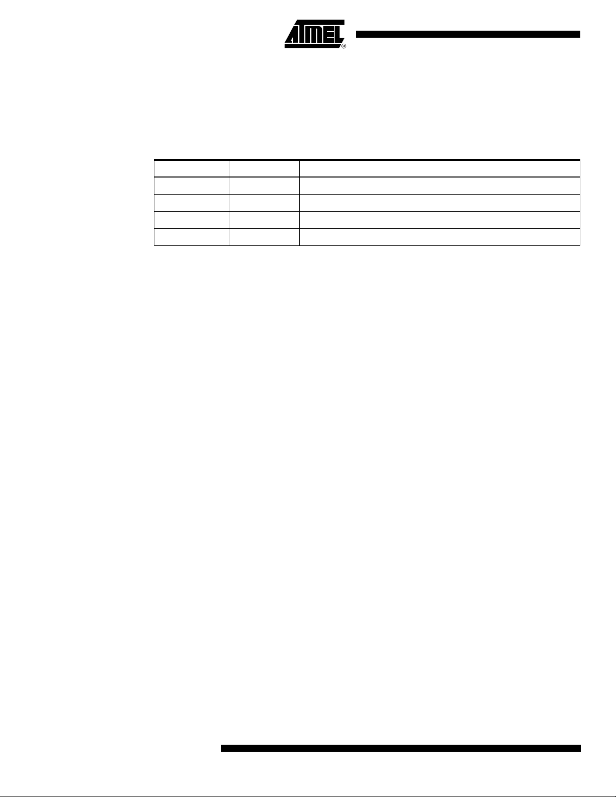
Pin Name Function
A0 - A20 Addresses
CE Chip Enable
OE
WE
RESET
VPP Write Protection
I/O0 - I/O15 Data Inputs/Outputs
NC No Connect
VCCQ Output Power Supply
WP
2.1 TSOP Top View (Type 1)
Output Enable
Write Enable
Reset
Write Protect
A15
A14
A13
A12
A11
A10
A9
A8
NC
A20
WE
RESET
VPP
WP
A19
A18
A17
A7
A6
A5
A4
A3
A2
A1
1
2
3
4
5
6
7
8
9
10
11
12
13
14
15
16
17
18
19
20
21
22
23
24
A16
48
VCCQ
47
GND
46
I/O15
45
I/O7
44
I/O14
43
I/O6
42
I/O13
41
I/O5
40
I/O12
39
I/O4
38
VCC
37
I/O11
36
I/O3
35
I/O10
34
I/O2
33
I/O9
32
I/O1
31
I/O8
30
I/O0
29
OE
28
GND
27
CE
26
A0
25
2.2 CBGA Top View (Ball Down)
2
AT49BV320D(T)
2 3 4567
1
8
A
A11
A13
A8
VPP
WP
A19
A7
A4
B
A10
A14
WE
RST
A18
A17
A5
A2
C
A12
A15
A9
A20
A6
A3
A1
D
A16
I/O14
I/O5
I/O11
I/O2
I/O8
CE
A0
E
VCCQ
I/O15
I/O6
I/O12
I/O3
I/O9
I/O0
GND
F
GND
I/O7
I/O13
I/O4
VCC
I/O10
I/O1
OE
3581D–FLASH–2/06
3. Block Diagram
AT49BV320D(T)
I/O0 - I/O15
A0 - A20
INPUT
BUFFER
ADDRESS
LATCH
Y-DECODER
X-DECODER
OUTPUT
BUFFER
OUTPUT
IDENTIFIER
MULTIPLEXER
COMPARATOR
MEMORY
REGISTER
STATUS
REGISTER
DATA
Y-GATING
MAIN
INPUT
BUFFER
DATA
REGISTER
COMMAND
REGISTER
WRITE STATE
MACHINE
PROGRAM/ERASE
VOLTAGE SWITCH
CE
WE
OE
RESET
WP
VPP
VCC
GND
4. Device Operation
4.1 Command Sequences
When the device is first powered on, it will be in the read mode. In order to perform other device
functions, a series of command sequences are entered into the device. The command
sequences are shown in the “Command Definition Table” on page 15 (I/O8 - I/O15 are don’t care
inputs for the command codes). The command sequences are written by applying a low pulse
on the WE
latched by the first rising edge of CE
The address locations used in the command sequences are not affected by entering the command sequences.
4.2 Read
When the AT49BV320D(T) is in the read mode, with CE and OE low and WE high, the data
stored at the memory location determined by the address pins are asserted on the outputs. The
3581D–FLASH–2/06
or CE input with CE or WE low (respectively) and OE high. The address and data are
or WE. Standard microprocessor write timings are used.
3

4.3 Reset
4.4 Erase
4.4.1 Sector Erase
outputs are put in the high impedance state whenever CE or OE is high. This dual-line control
gives designers flexibility in preventing bus contention.
A RESET input pin is provided to ease some system applications. When RESET is at a logic
high level, the device is in its standard operating mode. A low level on the RESET
present device operation and puts the outputs of the device in a high impedance state. When a
high level is reasserted on the RESET
the state of the control inputs.
Before a word can be reprogrammed, it must be erased. The erased state of memory bits is a
logical “1”. The individual sectors can be erased by using the Sector Erase command.
The device is organized into 71 sectors (SA0 - SA70) that can be individually erased. The Sector
Erase command is a two-bus cycle operation. The sector address and the D0H Data Input command are latched on the rising edge of WE
of the second cycle provided the given sector has not been protected. The erase operation is
internally controlled; it will automatically time to completion. The maximum time to erase a sector
is t
. An attempt to erase a sector that has been protected will result in the operation terminat-
SEC
ing immediately.
pin, the device returns to the read mode, depending upon
. The sector erase starts after the rising edge of WE
input halts the
4.5 Word Programming
Once a memory sector is erased, it is programmed (to a logical “0”) on a word-by-word basis.
Programming is accomplished via the Internal Device command register and is a two-bus cycle
operation. The device will automatically generate the required internal program pulses.
Any commands, except Read Status Register, Program Suspend and Program Resume, written
to the chip during the embedded programming cycle will be ignored. If a hardware reset happens during programming, the data at the location being programmed will be corrupted. Please
note that a data “0” cannot be programmed back to a “1”; only erase operations can convert “0”s
to “1”s. Programming is completed after the specified t
“1”, the device was not able to verify that the program operation was performed successfully.
The status register indicates the programming status. While the program sequence executes,
status bit I/O7 is “0”.
4.6 VPP Pin
The circuitry of the AT49BV320D(T) is designed so that the device cannot be programmed or
erased if the V
erase operations can be performed. The VPP pin cannot be left floating.
cycle time. If the program status bit is a
BP
voltage is less that 0.4V. When VPP is at 1.65V or above, normal program and
PP
4
AT49BV320D(T)
3581D–FLASH–2/06
4.7 Read Status Register
The status register indicates the status of device operations and the success/failure of that operation. The Read Status Register command causes subsequent reads to output data from the
status register until another command is issued. To return to reading from the memory, issue a
Read command.
The status register bits are output on I/O7 - I/O0. The upper byte, I/O15 - I/O8, outputs 00H
when a Read Status Register command is issued.
AT49BV320D(T)
The contents of the status register [SR7:SR0] are latched on the falling edge of OE
(whichever occurs last), which prevents possible bus errors that might occur if status register
contents change while being read. CE
or OE must be toggled with each subsequent status read,
or the status register will not indicate completion of a Program or Erase operation.
When the Write State Machine (WSM) is active, SR7 will indicate the status of the WSM; the
remaining bits in the status register indicate whether the WSM was successful in performing the
preferred operation (see Table 4-1).
Table 4-1. Status Register Bit Definition
WSMS ESS ES PS VPPS PSS SLS R
76543210
Notes
SR7 WRITE STATE MACHINE STATUS (WSMS)
1 = Ready
0 = Busy
SR6 = ERASE SUSPEND STATUS (ESS)
1 = Erase Suspended
0 = Erase In Progress/Completed
SR5 = ERASE STATUS (ES)
1 = Error in Sector Erase
0 = Successful Sector Erase
Check Write State Machine bit first to determine Word Program
or Sector Erase completion, before checking program or erase
status bits.
When Erase Suspend is issued, WSM halts execution and sets
both WSMS and ESS bits to “1” – ESS bit remains set to “1” until
an Erase Resume command is issued.
When this bit is set to “1”, WSM has applied the max number of
erase pulses to the sector and is still unable to verify successful
sector erasure.
or CE
SR4 = PROGRAM STATUS (PS)
1 = Error in Programming
0 = Successful Programming
SR3 = VPP STATUS (VPPS)
1 = VPP Low Detect, Operation Abort
0 = VPP OK
SR2 = PROGRAM SUSPEND STATUS (PSS)
1 = Program Suspended
0 = Program in Progress/Completed
SR1 = SECTOR LOCK STATUS (SLS)
1 = Prog/Erase attempted on a locked sector; Operation aborted.
0 = No operation to locked sectors
SR0 = RESERVED FOR FUTURE ENHANCEMENTS (R)
Note: 1. A Command Sequence Error is indicated when SR1, SR3, SR4 and SR5 are set.
3581D–FLASH–2/06
When this bit is set to “1”, WSM has attempted but failed to
program a word
The V
level. The WSM interrogates V
Erase command sequences have been entered and informs the
system if VPP has not been switched on. The VPP is also checked
before the operation is verified by the WSM.
When Program Suspend is issued, WSM halts execution and
sets both WSMS and PSS bits to “1”. PSS bit remains set to “1”
until a Program Resume command is issued.
If a Program or Erase operation is attempted to one of the locked
sectors, this bit is set by the WSM. The operation specified is
aborted and the device is returned to read status mode.
This bit is reserved for future use and should be masked out
when polling the status register.
status bit does not provide continuous indication of VPP
PP
level only after the Program or
PP
5

4.7.1 Clear Status Register
The WSM can set status register bits 1 through 7 and can clear bits 2, 6 and 7; but, the WSM
cannot clear status register bits 1, 3, 4 or 5. Because bits 1, 3, 4 and 5 indicate various error conditions, these bits can be cleared only through the Clear Status Register command. By allowing
the system software to control the resetting of these bits, several operations may be performed
(such as cumulatively programming several addresses or erasing multiple sectors in sequence)
before reading the status register to determine if an error occurred during those operations. The
status register should be cleared before beginning another operation. The Read command must
be issued before data can be read from the memory array. The status register can also be
cleared by resetting the device.
4.8 Flexible Sector Protection
The AT49BV320D(T) offers two sector protection modes, the Softlock and the Hardlock. The
Softlock mode is optimized as sector protection for sectors whose content changes frequently.
The Hardlock protection mode is recommended for sectors whose content changes infrequently.
Once either of these two modes is enabled, the contents of the selected sector is read-only and
cannot be erased or programmed. Each sector can be independently programmed for either the
Softlock or Hardlock sector protection mode. At power-up and reset, all sectors have their Softlock protection mode enabled.
4.8.1 Softlock and Unlock
The Softlock protection mode can be disabled by issuing a two-bus cycle Unlock command to
the selected sector. Once a sector is unlocked, its contents can be erased or programmed. To
enable the Softlock protection mode, a two-bus cycle Softlock command must be issued to the
selected sector.
4.8.2 Hardlock and Write Protect
The Hardlock sector protection mode operates in conjunction with the Write Protect (WP
The Hardlock sector protection mode can be enabled by issuing a two-bus cycle Hardlock Software command to the selected sector. The state of the Write Protect pin affects whether the
Hardlock protection mode can be overridden.
• When the WP
unlocked and the contents of the sector is read-only.
• When the WP
unlocked via the Unlock command.
To disable the Hardlock sector protection mode, the chip must be either reset or power cycled.
) pin.
pin is low and the Hardlock protection mode is enabled, the sector cannot be
pin is high, the Hardlock protection mode is overridden and the sector can be
6
AT49BV320D(T)
3581D–FLASH–2/06
AT49BV320D(T)
Table 4-2. Hardlock and Softlock Protection Configurations in Conjunction with WP
Erase/
Hard-
V
PP
/5V 0 0 0 Yes No sector is locked
V
CC
WP
lock
VCC/5V001 No
V
/5V011 No
CC
/5V 1 0 0 Yes No sector is locked.
V
CC
VCC/5V101 No
/5V110Yes
V
CC
VCC/5V111 No
Soft-
lock
Prog
Allowed? Comments
Sector is Softlocked. The Unlock command
can unlock the sector.
Hardlock protection mode is enabled. The
sector cannot be unlocked.
Sector is Softlocked. The Unlock command
can unlock the sector.
Hardlock protection mode is overridden and
the sector is not locked.
Hardlock protection mode is overridden and
the sector can be unlocked via the Unlock
command.
V
IL
xxx No
Figure 4-1. Sector Locking State Diagram
UNLOCKED LOCKED
60h/
D0h
6
0
60h/D0h
60h/
D0h
h
/
2
WP= V
WP = V
[000] [001]
=0
IL
[110]
=1
IH
[100]
Erase and Program Operations cannot be
performed.
60h/01h
F
h
60h/
2Fh
60h/
01h
60h/
01h
60h/
2Fh
[011]
[111]
[101]
Power-Up/Reset
Default
Hardlocked
Hardlocked is disabled by
WP = V
60h/
Power-Up/Reset
2Fh
Default
IH
3581D–FLASH–2/06
60h/D0h = Unlock Command
60h/01h = SoftlockCommand
60h/2Fh= Hardlock Command
Note: 1. The notation [X, Y, Z] denotes the locking state of a sector. The current locking state of a sector
is defined by the state of WP
and the two bits of the sector-lock status D[1:0].
7
4.8.3 Sector Protection Detection
A software method is available to determine if the sector protection Softlock or Hardlock features
are enabled. When the device is in the software product identification mode, a read from the
I/O0 and I/O1 at address location 00002H within a sector will show if the sector is unlocked, softlocked, or hardlocked.
Table 4-3. Sector Protection Status
I/O1 I/O0 Sector Protection Status
0 0 Sector Not Locked
0 1 Softlock Enabled
1 0 Hardlock Enabled
1 1 Both Hardlock and Softlock Enabled
4.9 Erase Suspend/Erase Resume
The Erase Suspend command allows the system to interrupt a sector erase operation and then
program or read data from a different sector within the memory. After the Erase Suspend command is given, the device requires a maximum time of 15 µs to suspend the erase operation.
After the erase operation has been suspended, the system can then read data or program data
to any other sector within the device. An address is not required during the Erase Suspend command. During a sector erase suspend, another sector cannot be erased. To resume the sector
erase operation, the system must write the Erase Resume command. The Erase Resume command is a one-bus cycle command. The only valid commands while erase is suspended are
Read Status Register, Product ID Entry, CFI Query, Program, Program Resume, Erase
Resume, Sector Softlock/Hardlock, Sector Unlock.
4.10 Program Suspend/Program Resume
The Program Suspend command allows the system to interrupt a programming operation and
then read data from a different word within the memory. After the Program Suspend command is
given, the device requires a maximum of 20 µs to suspend the programming operation. After the
programming operation has been suspended, the system can then read data from any other
word within the device. An address is not required during the program suspend operation. To
resume the programming operation, the system must write the Program Resume command. The
program suspend and resume are one-bus cycle commands. The command sequence for the
erase suspend and program suspend are the same and the command sequence for the erase
resume and program resume are the same. The only other valid commands while program is
suspended are Read Status Register, Product ID Entry, CFI Query and Program Resume.
4.11 Product Identification
The product identification mode identifies the device and manufacturer as Atmel. It may be
accessed by a software operation. For details, see “Operating Modes” on page 21.
4.12 128-bit Protection Register
The AT49BV320D(T) contains a 128-bit register that can be used for security purposes in system design. The protection register is divided into two 64-bit sectors. The two sectors are
designated as sector A and sector B. The data in sector A is non-changeable and is programmed at the factory with a unique number. The data in sector B is programmed by the user
and can be locked out such that data in the sector cannot be reprogrammed. To program sector
8
AT49BV320D(T)
3581D–FLASH–2/06

B in the protection register, the two-bus cycle Program Protection Register command must be
used as shown in the “Command Definition Table” on page 15. To lock out sector B, the two-bus
cycle Lock Protection Register command must be used as shown in the “Command Definition
Table” . Data bit D1 must be zero during the second bus cycle. All other data bits during the sec-
ond bus cycle are don’t cares. To determine whether sector B is locked out, use the status of
sector B protection command. If data bit D1 is zero, sector B is locked. If data bit D1 is one, sector B can be reprogrammed. Please see the “Protection Register Addressing Table” on page 16
for the address locations in the protection register. To read the protection register, the Product
ID Entry command is given followed by a normal read operation from an address within the protection register. After determining whether sector B is protected or not, or reading the protection
register, the Read command must be given to return to the read mode.
4.13 Common Flash Interface (CFI)
CFI is a published, standardized data structure that may be read from a flash device. CFI allows
system software to query the installed device to determine the configurations, various electrical
and timing parameters and functions supported by the device. CFI is used to allow the system to
learn how to interface to the flash device most optimally. The two primary benefits of using CFI
are ease of upgrading and second source availability. The command to enter the CFI Query
mode is a one-bus cycle command which requires writing data 98h to any address. The CFI
Query command can be written when the device is ready to read data or can also be written
when the part is in the product ID mode. Once in the CFI Query mode, the system can read CFI
data at the addresses given in “Common Flash Interface Definition Table” on page 27. To return
to the read mode, issue the Read command.
AT49BV320D(T)
4.14 Hardware Data Protection
The Hardware Data Protection feature protects against inadvertent programs to the
AT49BV320D(T) in the following ways: (a) V
function is inhibited. (b) V
device will automatically time out 10 ms (typical) before programming. (c) Program inhibit: holding any one of OE
less than V
ILPP
4.15 Input Levels
While operating with a 2.65V to 3.6V power supply, the address inputs and control inputs (OE,
CE
and WE) may be driven from 0 to 5.5V without adversely affecting the operation of the
device. The I/O lines can only be driven from 0 to V
4.16 Output Levels
For the AT49BV320D(T), output high levels (VOH) are equal to V
- 3.6V output levels, V
sense: if VCC is below 1.8V (typical), the program
CC
power-on delay: once VCC has reached the VCC sense level, the
CC
low, CE high or WE high inhibits program cycles. (d) Program inhibit: VPP is
.
+ 0.6V.
CCQ
- 0.1V (not VCC). For 2.65V
CCQ
must be tied to VCC.
CCQ
3581D–FLASH–2/06
9
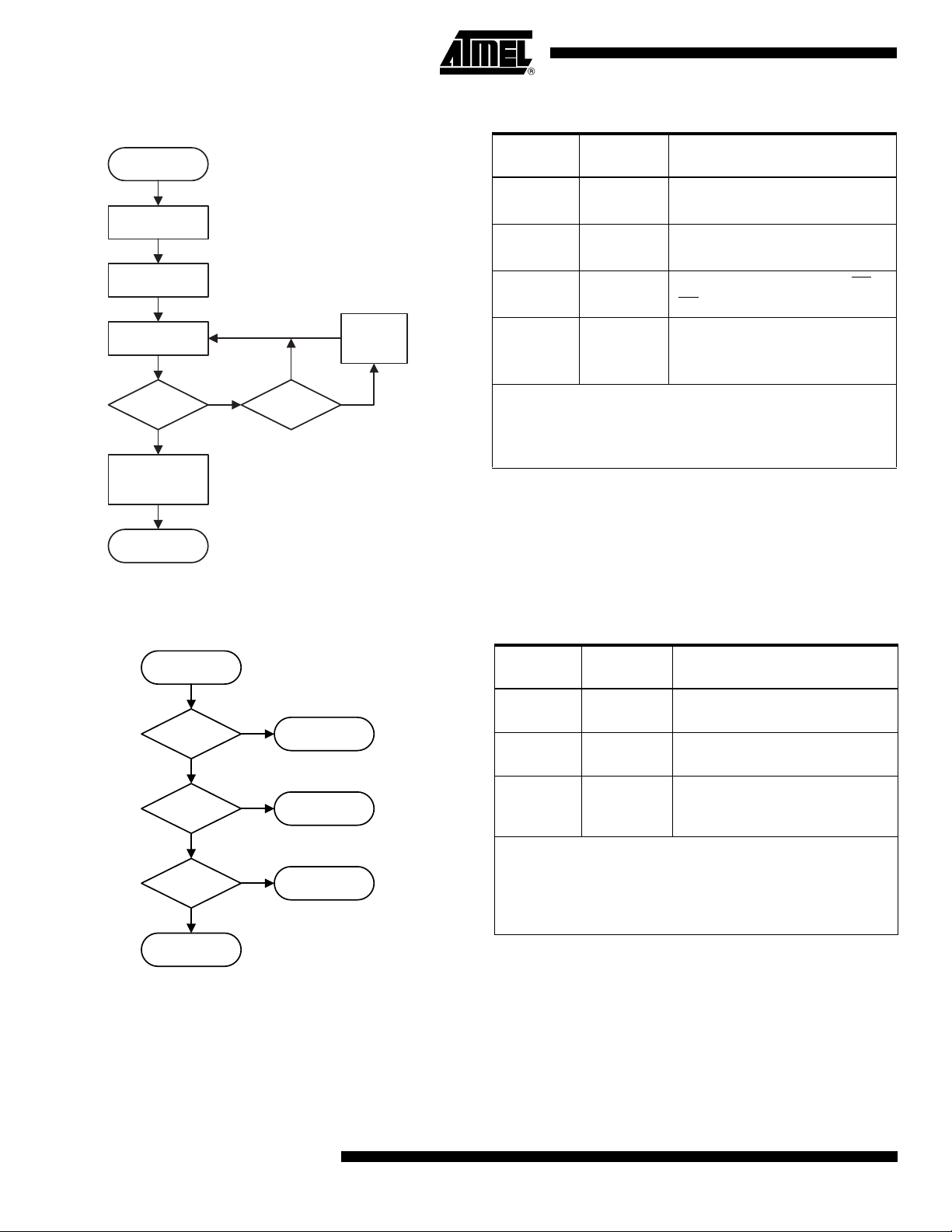
5. Word Program Flowchart
Start
6. Word Program Procedure
Bus
Operation Command Comments
Wri te 40,
Any Addr ess
Wr ite Data,
Wor d A ddr e ss
Read-Status
Regi ster
SR7 =
1
Full Status
Check
(If Desi red)
Progr am
Complete
(Setu p)
(Confirm)
0
No
Suspend?
Program
Suspend
Loop
Ye s
7. Full Status Check Flowchart
Read Status
Regi ster
SR3 =
1 V
0
PP
Error
Range
Write
Program
Setup
Write Data
Read None
Data = 40
Addr = Any Address
Data = Data to program
Addr = Location to program
Status register data: Toggle CE
to update status register
OE
Check SR7
Idle None
1 = WSM Ready
0 = WSM Busy
Repeat for subsequent Word Program operations.
Full status register check can be done after each program, or
after a sequence of program operations.
Write FF after the last operation to set to the Read state.
8. Full Status Check Procedure
Bus
Operation Command Comments
Idle None
Idle None
Check SR3:
Error
1 = V
PP
Check SR4:
1 = Data Program Error
or
10
SR4 =
0
SR1 =
0
Program
Successful
1
1
Program
Error
Device
Protect Err or
AT49BV320D(T)
Check SR1:
Idle None
1 = Sector locked;
operation aborted
SR3 MUST be cleared before the Write State Machine allows
further program attempts.
If an error is detected, clear the status register before
continuing operations – only the Clear Status Register
command clears the status register error bits.
3581D–FLASH–2/06

AT49BV320D(T)
9. Program Suspend/Resume Flowchart
Start
Wr i te B0
Any Address
Wr i te 70
Any Address
Read Status
Regi ster
SR7 =
1
SR2 =
1
Wr i te FF
Read
Data
(Program Suspend)
(Read Status)
0
0
Completed
(Read Array)
Wr i te F F
Program
(Re ad
Array)
10. Program Suspend/Resume Procedure
Bus
Operation Command Comments
Write
Write
Program
Suspend
Read
Status
Read None
Idle None
Idle None
Write Read Array
Read None
Write
Program
Resume
Data = B0
Addr = Any address
Data = 70
Addr = Any address
Status register data: Toggle CE
or
to update status register
OE
Addr = Any address
Check SR7
1 = WSM Ready
0 = WSM Busy
Check SR2
1 = Program suspended
0 = Program completed
Data = FF
Addr = Any address
Read data from any word in the
memory
Data = D0
Addr = Any address
Done
Reading
Yes
Wr i te D 0
Any Address
Program
Resumed
No
(Program Resume)
Read
Data
3581D–FLASH–2/06
11

11. Sector Erase Flowchart
Start
12. Sector Erase Procedure
Bus
Operation Command Comments
Wri te 2 0,
Addr ess
Any
Wri te D 0,
Addr ess
Sector
Read Status
Regist er
SR7 =
Full Er ase
Status Check
(IfDesired)
Sector
Complete
(Erase)
Sector
(Erase Confirm)
0 Ye s
1
Erase
No
Suspend
Eras e
Suspend
Eras e
Loop
13. Full Erase Status Check Flowchart
Read Status
Regist er
1
1,1
1
1
VPPRange
Error
Command
Sequenc e Err or
Sector
Eras e
Error
Sector
Lock ed
Error
SR3 =
SR4, SR5
SR5 =
SR1 =
Sector
Successful
0
=
0
0
0
Erase
Write
Write
Sector
Erase
Setup
Erase
Confirm
Data = 20
Addr = Any address
Data = D0
Addr = Sector to be erased (SA)
Status register data: Toggle CE
Read None
or
to update status register data
OE
Check SR7
Idle None
1 = WSM Ready
0 = WSM Busy
Repeat for subsequent sector erasures.
Full status register check can be done after each sector erase,
or after a sequence of sector erasures.
Write FF after the last operation to enter read mode.
14. Full Erase Status Check Procedure
Bus
Operation Command Comments
Idle None
Idle None
Idle None
Idle None
SR1, SR3 must be cleared before the Write State Machine
allows further erase attempts.
Only the Clear Status Register command clears SR1, SR3,
SR4, SR5.
If an error is detected, clear the status register before
attempting an erase retry or other error recovery.
Check SR3:
Range Error
1 = V
PP
Check SR4, SR5:
Both 1 = Command Sequence
Error
Check SR5:
1 = Sector Erase Error
Check SR1:
1 = Attempted erase of locked
sector; erase aborted.
12
AT49BV320D(T)
3581D–FLASH–2/06

AT49BV320D(T)
15. Erase Suspend/Resume Flowchart
Star t
(Rea d A rray)
(E ra se Re sum e )
Write B0,
Any Addr ess
Write 70,
Any Addr ess
Read Status
Regis ter
SR7 =
SR6 =
Wr it e F F
Read
Data
Done
Reading
Write D0,
Any Addr ess
1
1
1
(Erase Suspend)
(Read Status)
0
0
0
Erase
Completed
Wri te FF
(Rea d A rray)
16. Erase Suspend/Resume Procedure
Bus
Operation Command Comments
Write
Write
Erase
Suspend
Read
Status
Read None
Idle None
Idle None
Write
Read or
Write
Write
Read or
Program
None
Program
Resume
Data = B0
Addr = Any address
Data = 70
Addr = Any address
Status register data: Toggle CE
or
to update status register
OE
Addr = Any address
Check SR7
1 = WSM Ready
0 = WSM Busy
Check SR6
1 = Erase suspended
0 = Erase completed
Data = FF or 40
Addr = Any address
Read or program data from/to
sector other than the one being
erased
Data = D0
Addr = Any address
Erase
Resumed
Read Array
Data
3581D–FLASH–2/06
13

17. Protection Register Programming
18. Protection Register Programming
Flowchart
Start
Wri te C0,
Any Addr ess
Wri te PR
Addres s D ata
Read-Status
Register
SR7 =
1
Full-Status
Chec k
(If Des ired)
Progr am
Complete
(Program-Setup)
(Confirm Data )
0
Procedure
Bus
Operation Command Comments
Write
Write
Program
PR Setup
Protection
Program
Read None
Idle None
Program Protection Register operation addresses must be
within the protection register address space. Addresses
outside this space will return an error.
Repeat for subsequent programming operations.
Full status register check can be done after each program, or
after a sequence of program operations.
Write FF after the last operation to return to the Read mode.
Data = C0
Addr = Any address
Data = Data to Program
Addr = Location to Program
Status register data: Toggle CE
or
to update status register data
OE
Check SR7
1 = WSM Ready
0 = WSM Busy
19. Full Status Check Flowchart
Read Status
Register Data
SR3, SR4
SR3, SR4
SR3, SR4
Program
Successful
1
= VPPRangeError
0
1
1
Progr am Er ror
Regi ster Locked;
Progr am Abor ted
=
0
=
0
20. Full Status Check Procedure
Bus
Operation Command Comments
Idle None
Idle None
Idle None
SR3 must be cleared before the Write State Machine allows
further program attempts.
Only the Clear Status Register command clears SR1, SR3,
SR4.
If an error is detected, clear the status register before
attempting a program retry or other error recovery.
Check SR1, SR3, SR4:
0,1,1 = V
Range Error
PP
Check SR1, SR3, SR4:
0,0,1 = Programming Error
Check SR1, SR3, SR4:
1, 0,1 = Sector locked; operation
aborted
14
AT49BV320D(T)
3581D–FLASH–2/06

21. Command Definition Table
AT49BV320D(T)
Command Sequence
Bus
Cycles
1st Bus
Cycle
Addr Data Addr Data Addr Data
2nd Bus
Cycle
3rd Bus
Cycle
Read 1 XX FF
Sector Erase/Confirm 2 XX 20 SA
Word Program 2 XX 40/10 Addr D
Dual-word Program
(3)
3XXE0Addr0D
(2)
D0
IN
IN0
Addr1 D
IN1
Erase/Program Suspend 1 XX B0
Erase/Program Resume 1 XX D0
Product ID Entry 1 XX 90
Sector Softlock 2 XX 60 SA
Sector Hardlock 2 XX 60 SA
Sector Unlock 2 XX 60 SA
(2)
(2)
(2)
Read Status Register 2 XX 70 XX D
01
2F
D0
OUT
(4)
Clear Status Register 1 XX 50
Program Protection Register 2 XX C0 Addr
(5)
D
IN
Lock Protection Register – Sector B 2 XX C0 80 FFFD
Status of Sector B Protection 2 XX 90 80 D
OUT
(6)
CFI Query 1 XX 98
Notes: 1. The DATA FORMAT shown for each bus cycle is as follows; I/O7 - I/O0 (Hex). I/O15 - I/O8 are don’t care. The ADDRESS
FORMAT shown for each bus cycle is as follows: A7 - A0 (Hex). Address A20 through A8 are don’t care.
2. SA = sector address. Any word address within a sector can be used to designate the sector address (see pages 17 - 20 for
details).
3. This fast programming option enables the user to program two words in parallel only when V
Addr0 and Addr1, of the two words, D
IN0
and D
, must only differ in address A0. This command should be used during
IN1
= 9.5V. The addresses,
PP
manufacturing purposes only.
4. The status register bits are output on I/O7 - I/O0.
5. Any addresses within the user programmable protection register region. Address locations are shown on “Protection Regis-
ter Addressing Table” on page 16.
6. If data bit D1 is “0”, sector B is locked. If data bit D1 is “1”, sector B can be reprogrammed.
22. Absolute Maximum Ratings*
Temperature under Bias ................................ -55°C to +125°C
Storage Temperature ..................................... -65°C to +150°C
All Input Voltages
(including NC Pins)
with Respect to Ground ...................................-0.6V to +6.25V
All Output Voltages
with Respect to Ground .............................-0.6V to V
Voltage on V
PP
with Respect to Ground ...................................-0.6V to +10.0V
3581D–FLASH–2/06
+ 0.6V
CC
*NOTICE: Stresses beyond those listed under “Absolute
Maximum Ratings” may cause permanent damage to the device. This is a stress rating only and
functional operation of the device at these or any
other conditions beyond those indicated in the
operational sections of this specification is not
implied. Exposure to absolute maximum rating
conditions for extended periods may affect device
reliability.
15

23. Protection Register Addressing Table
AddressUseSectorA7A6A5A4A3A2A1A0
81FactoryA10000001
82FactoryA10000010
83FactoryA10000011
84FactoryA10000100
85UserB10000101
86UserB10000110
87UserB10000111
88UserB10001000
Note: All address lines not specified in the above table must be “0” when accessing the protection register, i.e., A20 - A8 = 0.
16
AT49BV320D(T)
3581D–FLASH–2/06

AT49BV320D(T)
24. AT49BV320D Sector Address Table
Sector Size (Bytes/Words) Address Range (A20 - A0)
SA0 8K/4K 00000 - 00FFF
SA1 8K/4K 01000 - 01FFF
SA2 8K/4K 02000 - 02FFF
SA3 8K/4K 03000 - 03FFF
SA4 8K/4K 04000 - 04FFF
SA5 8K/4K 05000 - 05FFF
SA6 8K/4K 06000 - 06FFF
SA7 8K/4K 07000 - 07FFF
SA8 64K/32K 08000 - 0FFFF
SA9 64K/32K 10000 - 17FFF
SA10 64K/32K 18000 - 1FFFF
SA11 64K/32K 20000 - 27FFF
SA12 64K/32K 28000 - 2FFFF
SA13 64K/32K 30000 - 37FFF
SA14 64K/32K 38000 - 3FFFF
SA15 64K/32K 40000 - 47FFF
SA16 64K/32K 48000 - 4FFFF
SA17 64K/32K 50000 - 57FFF
SA18 64K/32K 58000 - 5FFFF
SA19 64K/32K 60000 - 67FFF
SA20 64K/32K 68000 - 6FFFF
SA21 64K/32K 70000 - 77FFF
SA22 64K/32K 78000 - 7FFFF
SA23 64K/32K 80000 - 87FFF
SA24 64K/32K 88000 - 8FFFF
SA25 64K/32K 90000 - 97FFF
SA26 64K/32K 98000 - 9FFFF
SA27 64K/32K A0000 - A7FFF
SA28 64K/32K A8000 - AFFFF
SA29 64K/32K B0000 - B7FFF
SA30 64K/32K B8000 - BFFFF
SA31 64K/32K C0000 - C7FFF
SA32 64K/32K C8000 - CFFFF
SA33 64K/32K D0000 - D7FFF
SA34 64K/32K D8000 - DFFFF
SA35 64K/32K E0000 - E7FFF
SA36 64K/32K E8000 - EFFFF
SA37 64K/32K F0000 - F7FFF
3581D–FLASH–2/06
17

24. AT49BV320D Sector Address Table (Continued)
Sector Size (Bytes/Words) Address Range (A20 - A0)
SA38 64K/32K F8000 - FFFFF
SA39 64K/32K 100000 - 107FFF
SA40 64K/32K 108000 - 10FFFF
SA41 64K/32K 110000 - 117FFF
SA42 64K/32K 118000 - 11FFFF
SA43 64K/32K 120000 - 127FFF
SA44 64K/32K 128000 - 12FFFF
SA45 64K/32K 130000 - 137FFF
SA46 64K/32K 138000 - 13FFFF
SA47 64K/32K 140000 - 147FFF
SA48 64K/32K 148000 - 14FFFF
SA49 64K/32K 150000 - 157FFF
SA50 64K/32K 158000 - 15FFFF
SA51 64K/32K 160000 - 167FFF
SA52 64K/32K 168000 - 16FFFF
SA53 64K/32K 170000 - 177FFF
SA54 64K/32K 178000 - 17FFFF
SA55 64K/32K 180000 - 187FFF
SA56 64K/32K 188000 - 18FFFF
SA57 64K/32K 190000 - 197FFF
SA58 64K/32K 198000 - 19FFFF
SA59 64K/32K 1A0000 - 1A7FFF
SA60 64K/32K 1A8000 - 1AFFFF
SA61 64K/32K 1B0000 - 1B7FFF
SA62 64K/32K 1B8000 - 1BFFFF
SA63 64K/32K 1C0000 - 1C7FFF
SA64 64K/32K 1C8000 - 1CFFFF
SA65 64K/32K 1D0000 - 1D7FFF
SA66 64K/32K 1D8000 - 1DFFFF
SA67 64K/32K 1E0000 - 1E7FFF
SA68 64K/32K 1E8000 - 1EFFFF
SA69 64K/32K 1F0000 -1F7FFF
SA70 64K/32K 1F8000 - 1FFFFF
18
AT49BV320D(T)
3581D–FLASH–2/06

AT49BV320D(T)
25. AT49BV320DT – Sector Address Table
Sector Size (Bytes/Words) Address Range (A20 - A0)
SA0 64K/32K 00000 - 07FFF
SA1 64K/32K 08000 - 0FFFF
SA2 64K/32K 10000 - 17FFF
SA3 64K/32K 18000 - 1FFFF
SA4 64K/32K 20000 - 27FFF
SA5 64K/32K 28000 - 2FFFF
SA6 64K/32K 30000 - 37FFF
SA7 64K/32K 38000 - 3FFFF
SA8 64K/32K 40000 - 47FFF
SA9 64K/32K 48000 - 4FFFF
SA10 64K/32K 50000 - 57FFF
SA11 64K/32K 58000 - 5FFFF
SA12 64K/32K 60000 - 67FFF
SA13 64K/32K 68000 - 6FFFF
SA14 64K/32K 70000 - 77FFF
SA15 64K/32K 78000 - 7FFFF
SA16 64K/32K 80000 - 87FFF
SA17 64K/32K 88000 - 8FFFF
SA18 64K/32K 90000 - 97FFF
SA19 64K/32K 98000 - 9FFFF
SA20 64K/32K A0000 - A7FFF
SA21 64K/32K A8000 - AFFFF
SA22 64K/32K B0000 - B7FFF
SA23 64K/32K B8000 - BFFFF
SA24 64K/32K C0000 - C7FFF
SA25 64K/32K C8000 - CFFFF
SA26 64K/32K D0000 - D7FFF
SA27 64K/32K D8000 - DFFFF
SA28 64K/32K E0000 - E7FFF
SA29 64K/32K E8000 - EFFFF
SA30 64K/32K F0000 - F7FFF
SA31 64K/32K F8000 - FFFFF
SA32 64K/32K 100000 - 107FFF
SA33 64K/32K 108000 - 10FFFF
SA34 64K/32K 110000 - 117FFF
SA35
SA36
SA37 64K/32K 128000 - 12FFFF
64K/32K 118000 - 11FFFF
64K/32K 120000 - 127FFF
3581D–FLASH–2/06
19

25. AT49BV320DT – Sector Address Table (Continued)
Sector Size (Bytes/Words) Address Range (A20 - A0)
SA38 64K/32K 130000 - 137FFF
SA39 64K/32K 138000 - 13FFFF
SA40 64K/32K 140000 - 147FFF
SA41 64K/32K 148000 - 14FFFF
SA42 64K/32K 150000 - 157FFF
SA43 64K/32K 158000 - 15FFFF
SA44 64K/32K 160000 - 167FFF
SA45 64K/32K 168000 - 16FFFF
SA46 64K/32K 170000 - 177FFF
SA47 64K/32K 178000 - 17FFFF
SA48 64K/32K 180000 - 187FFF
SA49 64K/32K 188000 - 18FFFF
SA50 64K/32K 190000 - 197FFF
SA51 64K/32K 198000 - 19FFFF
SA52 64K/32K 1A0000 - 1A7FFF
SA53 64K/32K 1A8000 - 1AFFFF
SA54 64K/32K 1B0000 - 1B7FFF
SA55 64K/32K 1B8000 - 1BFFFF
SA56 64K/32K 1C0000 - 1C7FFF
SA57 64K/32K 1C8000 - 1CFFFF
SA58 64K/32K 1D0000 - 1D7FFF
SA59 64K/32K 1D8000 - 1DFFFF
SA60 64K/32K 1E0000 - 1E7FFF
SA61 64K/32K 1E8000 - 1EFFFF
SA62 64K/32K 1F0000 - 1F7FFF
SA63 8K/4K 1F8000 - 1F8FFF
SA64 8K/4K 1F9000 - 1F9FFF
SA65 8K/4K 1FA000 - 1FAFFF
SA66 8K/4K 1FB000 - 1FBFFF
SA67 8K/4K 1FC000 - 1FCFFF
SA68 8K/4K 1FD000 - 1FDFFF
SA69 8K/4K 1FE000 - 1FEFFF
SA70 8K/4K 1FF000 - 1FFFFF
20
AT49BV320D(T)
3581D–FLASH–2/06

AT49BV320D(T)
26. DC and AC Operating Range
AT49BV320D(T)-70
Operating Temperature (Case) Ind. -40°C - 85°C
VCC Power Supply 2.65V to 3.6V
27. Operating Modes
V
PP
X
IHPP
(1)
(2)
(4)
Ai I/O
Ai D
Ai D
X
(5)
V
ILPP
X X High-Z
A0 = VIL, A1 - A20 = VILManufacturer Code
A0 = VIH, A1 - A20 = V
IL
Mode CE OE WE RESET V
Read V
Program/Erase
(3)
Standby/Program Inhibit V
IL
V
IL
IH
V
V
X
XXV
Program Inhibit
XV
XXXV
Output Disable X V
Reset XXXV
Product Identification
Software
V
IL
IH
(2)
IL
IH
IH
V
IL
XVIHX X High-Z
IH
XVIHX
XVIHX High-Z
V
IH
V
IH
V
IH
IH
IL
V
IH
Notes: 1. The VPP pin can be tied to VCC. For faster program operations, VPP can be set to 9.5V ± 0.5V.
2. X can be V
or VIH.
IL
3. Refer to AC programming waveforms on page 26.
4. V
5. V
(min) = 1.65V.
IHPP
(max) = 0.4V.
ILPP
6. Manufacturer Code: 001FH, Device Code: 90C5H – AT49BV320D; 90C4H – AT49BV320DT
OUT
IN
Device Code
(6)
(6)
3581D–FLASH–2/06
21

28. DC Characteristics
Symbol Parameter Condition Min Typ Max Units
I
I
I
I
I
I
V
V
V
V
LI
LO
SB
CC
CC1
PP1
IL
IH
OL
OH
(1)
Input Load Current VIN = 0V to V
Output Leakage Current V
VCC Standby Current CMOS CE = VCC - 0.3V to V
V
Active Read Current f = 5 MHz; I
CC
VCC Programming Current 25 mA
VPP Input Load Current 10 µA
Input Low Voltage 0.6 V
Input High Voltage V
Output Low Voltage IOL = 2.1 mA 0.45 V
Output High Voltage IOH = -100 µA V
Note: 1. In the erase mode, ICC is 25 mA.
= 0V to V
I/O
CC
CC
CC
= 0 mA 10 15 mA
OUT
- 0.6 V
CCQ
- 0.1 V
CCQ
15 25 µA
2µA
2µA
22
AT49BV320D(T)
3581D–FLASH–2/06

29. Input Test Waveforms and Measurement Level
2.0V
1.5V
0.6V
tR, tF < 5 ns
30. Output Test Load
V
CCQ
1.8
AT49BV320D(T)
1.3
30
31. Pin Capacitance
f = 1 MHz, T = 25°C
Symbol Typ Max Units Conditions
C
IN
C
OUT
Note: This parameter is characterized and is not 100% tested.
(1)
46pFV
812pFV
IN
OUT
= 0V
= 0V
3581D–FLASH–2/06
23

32. AC Read Characteristics
Symbol Parameter
AT49BV320D(T)-70
UnitsMin Max
t
t
t
t
t
t
t
RC
ACC
CE
OE
DF
OH
RO
(1)
(2)
(3)(4)
Read Cycle Time 70 ns
Address to Output Delay 70 ns
CE to Output Delay 70 ns
OE to Output Delay 0 20 ns
CE or OE to Output Float 0 25 ns
Output Hold from OE, CE or Address,
whichever occurred first
RESET to Output Delay 100 ns
33. AC Read Waveforms
ADDRESS
CE
OE
(1)(2)(3)(4)
t
RC
ADDRESS VALID
t
CE
t
OE
t
ACC
0ns
t
DF
t
OH
RESET
OUTPUT
Notes: 1. CE may be delayed up to t
may be delayed up to tCE - tOE after the falling edge of CE without impact on tCE or by t
2. OE
without impact on t
ACC
.
3. tDF is specified from OE or CE, whichever occurs first (CL = 5 pF).
4. This parameter is characterized and is not 100% tested.
t
RO
HIGH Z
- tCE after the address transition without impact on t
ACC
OUTPUT
VALID
ACC
.
- tOE after an address change
ACC
24
AT49BV320D(T)
3581D–FLASH–2/06

AT49BV320D(T)
34. AC Word Load Characteristics
Symbol Parameter Min Max Units
, t
t
AS
OES
t
AH
t
CS
t
CH
t
WP
t
WPH
t
DS
t
, t
DH
OEH
35. AC Word Load Waveforms
35.1 WE Controlled
Address, OE Setup Time 20 ns
Address Hold Time 0 ns
Chip Select Setup Time 0 ns
Chip Select Hold Time 0 ns
Write Pulse Width (WE or CE)25ns
Write Pulse Width High 15 ns
Data Setup Time 25 ns
Data, OE Hold Time 0 ns
35.2 CE
3581D–FLASH–2/06
Controlled
25

36. Program Cycle Characteristics
Symbol Parameter Min Typ Max Units
t
BP
t
BPD
t
AS
t
AH
t
DS
t
DH
t
WP
t
WPH
t
WC
t
RP
t
SEC1
t
SEC2
t
ES
t
PS
Word Programming Time 10 120 µs
Word Programming Time in Dual Programming Mode 5 60 µs
Address Setup Time 20 ns
Address Hold Time 0 ns
Data Setup Time 25 ns
Data Hold Time 0 ns
Write Pulse Width 25 ns
Write Pulse Width High 15 ns
Write Cycle Time 70 ns
Reset Pulse Width 500 ns
Sector Erase Cycle Time (4K Word Sectors) 0.1 2 seconds
Sector Erase Cycle Time (32K Word Sectors) 0.5 6.0 seconds
Erase Suspend Time 15 µs
Program Suspend Time 10 µs
37. Program Cycle Waveforms
PROGRAM CYCLE
OE
CE
WE
A0 - A20
DATA
tASt
(1)
XX
t
WC
Note 3
AH
t
WPH
ADDRESS
38. Sector Erase Cycle Waveforms
(2)
OE
CE
t
t
AS
XX
(1)
t
WC
WORD 0
t
WPH
t
AH
(4)
SA
20
WE
A0-A20
DATA
Notes: 1. Any address can be used to load the data.
must be high only when WE and CE are both low.
2. OE
3. The data can be 40H or 10H.
4. The address depends on what sector is to be erased.
t
WP
t
DS
INPUT DATA
WP
t
t
DS
D0
WORD 1
t
BP
t
DH
DH
t
EC
26
AT49BV320D(T)
3581D–FLASH–2/06

39. Common Flash Interface Definition Table
AT49BV320D(T)
Address AT49BV320DT AT49BV320D
10h 0051h 0051h “Q”
11h 0052h 0052h “R”
12h 0059h 0059h “Y”
13h 0003h 0003h
14h 0000h 0000h
15h 0041h 0041h
16h 0000h 0000h
17h 0000h 0000h
18h 0000h 0000h
19h 0000h 0000h
1Ah 0000h 0000h
1Bh 0027h 0027h VCC min write/erase
1Ch 0036h 0036h VCC max write/erase
1Dh 0090h 0090h VPP min voltage
1Eh 00A0h 00A0h VPP max voltage
1Fh 0004h 0004h Typ word write – 10 µs
20h 0002h 0002h Typ dual word program time – 5 µs
21h 0009h 0009h Typ sector erase, 500 ms
22h 0000h 0000h Typ chip erase, not supported
23h 0004h 0004h Max word write/typ time
24h 0004h 0004h Max dual word program time/typ time
25h 0004h 0004h Max sector erase/typ sector erase
26h 0000h 0000h Max chip erase/ typ chip erase
27h 0016h 0016h Device size
28h 0001h 0001h x16 device
29h 0000h 0000h x16 device
2Ah 0002h 0002h Maximum number of bytes in multiple byte write = 4
2Bh 0000h 0000h Maximum number of bytes in multiple byte write = 4
2Ch 0002h 0002h 2 regions, x = 2
2Dh 003Eh 0007h 64K bytes, Y = 62 (Top); 8K bytes, Y = 7 (Bottom)
2Eh 0000h 0000h 64K bytes, Y = 62 (Top); 8K bytes, Y = 7 (Bottom)
2Fh 0000h 0020h 64K bytes, Z = 256 (Top); 8K bytes, Z = 32 (Bottom)
30h 0001h 0000h 64K bytes, Z = 256 (Top); 8K bytes, Z = 32 (Bottom)
31h 0007h 003Eh 8K bytes, Y = 7 (Top); 64K bytes, Y = 62 (Bottom)
32h 0000h 0000h 8K bytes, Y = 7 (Top); 64K bytes, Y = 62 (Bottom)
33h 0020h 0000h 8K bytes, Z = 32 (Top); 64K bytes, Z = 256 (Bottom)
34h 0000h 0001h 8K bytes, Z = 32 (Top); 64K bytes, Z = 256 (Bottom)
Comments
3581D–FLASH–2/06
27

39. Common Flash Interface Definition Table (Continued)
Address AT49BV320DT AT49BV320D
VENDOR SPECIFIC EXTENDED QUERY
41h 0050h 0050h “P”
42h 0052h 0052h “R”
43h 0049h 0049h “I”
44h 0031h 0031h Major version number, ASCII
45h 0030h 0030h Minor version number, ASCII
46h 0086h 0086h
47h 0000h 0001h Bit 8 – top (“0”) or bottom (“1”) boot sector device undefined bits are “0”
48h 0000h 0000h
Comments
Bit 0 – chip erase supported, 0 – no, 1 – yes
Bit 1 – erase suspend supported, 0 – no, 1 – yes
Bit 2 – program suspend supported, 0 – no, 1 – yes
Bit 3 – simultaneous operations supported,
0 – no, 1 – yes
Bit 4 – burst mode read supported, 0 – no, 1 – yes
Bit 5 – page mode read supported, 0 – no, 1 – yes
Bit 6 – queued erase supported, 0 – no, 1 – yes
Bit 7 – protection bits supported, 0 – no, 1 – yes
Bit 0 – 4 word linear burst with wrap around,
0 – no, 1 – yes
Bit 1 – 8 word linear burst with wrap around,
0 – no, 1 – yes
Bit 2 – continuos burst, 0 - no, 1 - yes
Undefined bits are “0”
Bit 0 – 4 word page, 0 – no, 1 – yes
49h 0000h 0000h
4Ah 0080h 0080h Location of protection register lock byte, the section’s first byte
4Bh 0003h 0003h # of bytes in the factory prog section of prot register – 2*n
4Ch 0003h 0003h # of bytes in the user prog section of prot register – 2*n
Bit 1 – 8 word page, 0 – no, 1 – yes
Undefined bits are “0”
28
AT49BV320D(T)
3581D–FLASH–2/06

40. Ordering Information
40.1 Green Package (Pb/Halide-free)
I
(mA)
t
ACC
(ns)
CC
Ordering Code Package Operation RangeActive Standby
AT49BV320D(T)
70 25 0.025
AT49BV320D-70CU
AT49BV320D-70TU
AT49BV320DT-70CU
AT49BV320DT-70TU
47C1
48T
47C1
48T
Industrial
(-40° to 85° C)
Package Type
47C1 47-ball, Plastic Chip-Size Ball Grid Array Package (CBGA)
48T 48-lead, Plastic Thin Small Outline Package (TSOP)
3581D–FLASH–2/06
29

41. Packaging Information
41.1 47C1 – CBGA
E
A1 BALL ID
D
0.875 REF
TOP VIEW
A
E1
e
A
B
C
D
E
F
7 65432
8
b
BOTTOM VIEW
1
A1 BALL CORNER
3.125 REF
SYMBOL
D1
SIDE VIEW
E 6.90 7.00 7.10
E1 5.25 TYP
D 9.90 10.00 10.10
D1 3.75 TYP
A – – 1.00
A1 0.22 – –
e 0.75 BSC
b 0.35 TYP
A1
COMMON DIMENSIONS
(Unit of Measure = mm)
MIN
NOM
MAX
NOTE
30
2325 Orchard Parkway
R
San Jose, CA 95131
47C1, 47-ball (8 x 6 Array), 0.75 mm Pitch,
7.0 x 10.0 x 1.0 mm Chip-scale Ball Grid Array Package (CBGA)
AT49BV320D(T)
TITLE
DRAWING NO.
47C1
3581D–FLASH–2/06
7/2/03
REV.
A

41.2 48T – TSOP
AT49BV320D(T)
PIN 1
Pin 1 Identifier
D1
D
e
E
b
A2
A
SEATING PLANE
A1
Notes: 1. This package conforms to JEDEC reference MO-142, Variation DD.
2. Dimensions D1 and E do not include mold protrusion. Allowable
protrusion on E is 0.15 mm per side and on D1 is 0.25 mm per side.
3. Lead coplanarity is 0.10 mm maximum.
0º ~ 8º
L
COMMON DIMENSIONS
SYMBOL
A – – 1.20
A1 0.05 – 0.15
A2 0.95 1.00 1.05
D 19.80 20.00 20.20
D1 18.30 18.40 18.50 Note 2
E 11.90 12.00 12.10 Note 2
L 0.50 0.60 0.70
L1 0.25 BASIC
b 0.17 0.22 0.27
c 0.10 – 0.21
e 0.50 BASIC
c
L1
GAGE PLANE
(Unit of Measure = mm)
MIN
NOM
MAX
NOTE
2325 Orchard Parkway
R
San Jose, CA 95131
3581D–FLASH–2/06
TITLE
48T, 48-lead (12 x 20 mm Package) Plastic Thin Small Outline
Package, Type I (TSOP)
DRAWING NO.
48T
10/18/01
REV.
B
31

42. Revision History
Revision No. History
Revision A – Sept. 2005
Revision B – Oct. 2005 • Added Top Boot version.
Revision C – Nov. 2005 • Added CBGA Package Option.
Revision D – Feb. 2006 • Changed the AT49BV320DT CFI values of addresses 23h & 25h
• Initial Release
• Added Sector Address Table for the AT49BV320DT.
• Added CFI information for the AT49BV320DT.
• Modified Program Suspend/Resume Procedure on page 11
to match the flow chart.
• Modified Erase Suspend/Resume Procedure on page 13 to match
the flow chart.
• Changed the CFI values of addresses 20h & 24h to 0002h and
0004h, respectively.
to 0004h and 0004h, respectively.
32
AT49BV320D(T)
3581D–FLASH–2/06
 Loading...